

Page 1
EFM32PG22 Gecko MCU Family Data
Sheet
The EFM32PG22 Gecko family of microcontrollers is part of the
Series 2 Gecko portfolio. EFM32PG22 Gecko MCUs are ideal for
enabling energy-friendly embedded applications.
The highly efficient solution contains a 76.8 MHz Cortex-M33 with rich analog and communication peripherals to provide an industry-leading, energy efficient MCU for consumer and industrial applications.
Gecko applications include:
• Personal Hygiene devices
• Appliances and whitegoods
• Industrial Automation
• Consumer electronics
Core / Memory
ARM Cortex
with DSP, FPU and TrustZone
TM
M33 processor
ETM Debug Interface RAM Memory
Flash Program
Memory
LDMA
Controller
Clock Management
HF Crystal
Oscillator
Fast Startup
RC Oscillator
LF Crystal
Oscillator
RC Oscillator
RC Oscillator
Precision LF
Ultra LF RC
Oscillator
KEY FEATURES
• 32-bit ARM® Cortex®-M33 core with 76.8
MHz maximum operating frequency
• Up to 512 kB of flash and 32 kB of RAM
• Low energy operation
• 26 uA/MHz (EM0)
• 1.10 uA sleep (EM2)
• Secure Boot with Root of Trust and
Secure Loader (RTSL)
• 16-bit ADC with 16-channel scan
Energy Management
HF
Voltage
Regulator
Power-On
Reset
DC-DC
Converter
Brown-Out
Detector
32-bit bus
Peripheral Reflex System
Security
AES-128, AES-256,
SHA-1, SHA-2,
ECC
Secure Boot RTSL
Secure Debug
True Random Number
Generator
Lowest power mode with peripheral operational:
Serial Interfaces I/O Ports
USART
PDM
EUART
2
I
External
Interrupts
General
Purpose I/O
Pin Reset
C
Pin Wakeup
Timers and Triggers
Timer/Counter
Low Energy Timer Watchdog Timer
Real Time
Capture Counter
EM3—StopEM2—Deep SleepEM1—SleepEM0—Active
Protocol Timer
Back-Up Real
Time Counter
Analog I/F
ADC
Temperature
Sensor
EM4—Shutoff
silabs.com | Building a more connected world. Rev. 1.0
Page 2

1. Feature List
The EFM32PG22 highlighted features are listed below.
• Low Power MCU
•
High Performance 32-bit 76.8 MHz ARM Cortex®-M33 with
DSP instruction and floating-point unit for efficient signal
processing
• Up to 512 kB flash program memory
• Up to 32 kB RAM data memory
• Low System Energy Consumption
• 26 μA/MHz in Active Mode (EM0) at 38.4 MHz
• 1.10 μA EM2 DeepSleep current (8 kB RAM retention and
RTC running from LFRCO)
• 0.95 μA EM3 DeepSleep current (8 kB RAM retention and
RTC running from ULFRCO)
• 0.17 μA EM4 current
• Security Features
• Secure Boot with Root of Trust and Secure Loader (RTSL)
• Hardware Cryptographic Acceleration for AES128/256,
SHA-1, SHA-2 (up to 256-bit), ECC (up to 256-bit), ECDSA,
and ECDH
• True Random Number Generator (TRNG) compliant with
NIST SP800-90 and AIS-31
•
ARM® TrustZone
• Secure Debug with lock/unlock
• Packages
• QFN40 5 mm × 5 mm × 0.85 mm
• QFN32 4 mm × 4 mm × 0.85 mm
®
EFM32PG22 Gecko MCU Family Data Sheet
Feature List
• Wide selection of MCU peripherals
• Analog to Digital Converter (ADC)
• 12-bit @ 1 Msps
• 16-bit @ 76.9 ksps
• Up to 26 General Purpose I/O pins with output state retention and asynchronous interrupts
• 8 Channel DMA Controller
• 12 Channel Peripheral Reflex System (PRS)
• 4 × 16-bit Timer/Counter with 3 Compare/Capture/PWM
channels
• 1 × 32-bit Timer/Counter with 3 Compare/Capture/PWM
channels
• 32-bit Real Time Counter
• 24-bit Low Energy Timer for waveform generation
• 1 × Watchdog Timer
• 2 × Universal Synchronous/Asynchronous Receiver/Transmitter (UART/SPI/SmartCard (ISO 7816)/IrDA/I2S)
• 1 × Enhanced Universal Asynchronous Receiver/Transmitter (EUART)
•
2 × I2C interface with SMBus support
• Digital microphone interface (PDM)
• Die temperature sensor with +/-1.5 °C accuracy after singlepoint calibration
• Wide Operating Range
• 1.71 V to 3.8 V single power supply
• -40 °C to 125 °C
silabs.com | Building a more connected world. Rev. 1.0 | 2
Page 3
2. Ordering Information
EFM32PG22 Gecko MCU Family Data Sheet
Ordering Information
Table 2.1. Ordering Information
Flash
Ordering Code Max CPU Speed
EFM32PG22C200F128IM32-C 76.8 MHz 128 32 18 QFN32 -40 to 125 °C
EFM32PG22C200F128IM40-C 76.8 MHz 128 32 26 QFN40 -40 to 125 °C
EFM32PG22C200F256IM32-C 76.8 MHz 256 32 18 QFN32 -40 to 125 °C
EFM32PG22C200F256IM40-C 76.8 MHz 256 32 26 QFN40 -40 to 125 °C
EFM32PG22C200F512IM32-C 76.8 MHz 512 32 18 QFN32 -40 to 125 °C
EFM32PG22C200F512IM40-C 76.8 MHz 512 32 26 QFN40 -40 to 125 °C
EFM32PG22C200F64IM32-C 76.8 MHz 64 32 18 QFN32 -40 to 125 °C
EFM32PG22C200F64IM40-C 76.8 MHz 64 32 26 QFN40 -40 to 125 °C
(kB)
RAM
(kB) GPIO Package Temp Range
silabs.com | Building a more connected world. Rev. 1.0 | 3
Page 4

Table of Contents
1. Feature List ................................2
2. Ordering Information ............................3
3. System Overview ..............................7
3.1 Introduction ...............................7
3.2 General Purpose Input/Output (GPIO) ......................7
3.3 Clocking ................................8
3.3.1 Clock Management Unit (CMU) .......................8
3.3.2 Internal and External Oscillators.......................8
3.4 Counters/Timers and PWM ..........................8
3.4.1 Timer/Counter (TIMER) .........................8
3.4.2 Low Energy Timer (LETIMER) .......................8
3.4.3 Real Time Clock with Capture (RTCC) ....................8
3.4.4 Back-Up Real Time Counter (BURTC) ....................8
3.4.5 Watchdog Timer (WDOG) .........................8
3.5 Communications and Other Digital Peripherals ...................9
3.5.1 Universal Synchronous/Asynchronous Receiver/Transmitter (USART) ..........9
3.5.2 Enhanced Universal Asynchronous Receiver/Transmitter (EUART) ...........9
3.5.3 Inter-Integrated Circuit Interface (I2C) .....................9
3.5.4 Peripheral Reflex System (PRS) ......................9
3.5.5 Pulse Density Modulation (PDM) Interface ...................9
3.6 Security Features .............................9
3.6.1 Secure Boot with Root of Trust and Secure Loader (RTSL) .............9
3.6.2 Cryptographic Accelerator.........................10
3.6.3 True Random Number Generator ......................10
3.6.4 Secure Debug with Lock/Unlock.......................10
3.7 Analog.................................10
3.7.1 Analog to Digital Converter (IADC) ......................10
3.8 Power .................................11
3.8.1 Energy Management Unit (EMU) ......................11
3.8.2 Voltage Scaling ............................11
3.8.3 DC-DC Converter ...........................11
3.8.4 Power Domains ............................11
3.9 Reset Management Unit (RMU) ........................12
3.10 Core and Memory ............................12
3.10.1 Processor Core ............................12
3.10.2 Memory System Controller (MSC) .....................12
3.10.3 Linked Direct Memory Access Controller (LDMA) ................12
3.11 Memory Map ..............................13
3.12 Configuration Summary ..........................14
4. Electrical Specifications ..........................15
4.1 Electrical Characteristics ..........................15
silabs.com
| Building a more connected world. Rev. 1.0 | 4
Page 5

4.2 Absolute Maximum Ratings..........................16
4.3 General Operating Conditions .........................17
4.4 DC-DC Converter .............................18
4.4.1 DC-DC Operating Limits .........................20
4.5 Thermal Characteristics ...........................21
4.6 Current Consumption ............................22
4.6.1 MCU current consumption using DC-DC at 3.0 V input ...............22
4.6.2 MCU current consumption at 3.0 V ......................24
4.6.3 MCU current consumption at 1.8 V ......................26
4.7 Flash Characteristics ............................28
4.8 Wake Up, Entry, and Exit times ........................29
4.9 Oscillators ...............................30
4.9.1 High Frequency Crystal Oscillator ......................30
4.9.2 Low Frequency Crystal Oscillator ......................31
4.9.3 High Frequency RC Oscillator (HFRCO) ....................32
4.9.4 Fast Start_Up RC Oscillator (FSRCO).....................33
4.9.5 Low Frequency RC Oscillator (LFRCO) ....................34
4.9.6 Ultra Low Frequency RC Oscillator ......................34
4.10 GPIO Pins (3V GPIO pins) .........................35
4.11 Analog to Digital Converter (IADC) .......................37
4.12 Temperature Sense ............................39
4.13 Brown Out Detectors ...........................40
4.13.1 DVDD BOD .............................40
4.13.2 LE DVDD BOD ............................40
4.13.3 AVDD and IOVDD BODs ........................41
4.14 PDM Timing Specifications .........................42
4.14.1 Pulse Density Modulator (PDM), Common DBUS ................42
4.15 USART SPI Master Timing .........................43
4.15.1 SPI Master Timing, Voltage Scaling = VSCALE2.................44
4.15.2 SPI Master Timing, Voltage Scaling = VSCALE1.................44
4.16 USART SPI Slave Timing ..........................45
4.16.1 SPI Slave Timing, Voltage Scaling = VSCALE2 .................45
4.16.2 SPI Slave Timing, Voltage Scaling = VSCALE1 .................46
4.17 I2C Electrical Specifications .........................47
4.17.1 I2C Standard-mode (Sm) ........................47
4.17.2 I2C Fast-mode (Fm) ..........................48
4.17.3 I2C Fast-mode Plus (Fm+) ........................49
4.18 Typical Performance Curves .........................49
4.18.1 Supply Current ............................50
4.18.2 DC-DC Converter ...........................51
4.18.3 IADC ...............................52
5. Typical Connections ...........................53
5.1 Power .................................53
silabs.com
| Building a more connected world. Rev. 1.0 | 5
Page 6

5.2 Other Connections.............................54
6. Pin Definitions ..............................55
6.1 QFN32 Device Pinout ...........................55
6.2 QFN40 Device Pinout ...........................57
6.3 Alternate Function Table...........................59
6.4 Analog Peripheral Connectivity ........................59
6.5 Digital Peripheral Connectivity .........................60
7. QFN32 Package Specifications........................ 63
7.1 QFN32 Package Dimensions .........................63
7.2 QFN32 PCB Land Pattern ..........................65
7.3 QFN32 Package Marking ..........................67
8. QFN40 Package Specifications........................ 68
8.1 QFN40 Package Dimensions .........................68
8.2 QFN40 PCB Land Pattern ..........................70
8.3 QFN40 Package Marking ..........................71
9. Revision History .............................72
silabs.com
| Building a more connected world. Rev. 1.0 | 6
Page 7
EFM32PG22 Gecko MCU Family Data Sheet
System Overview
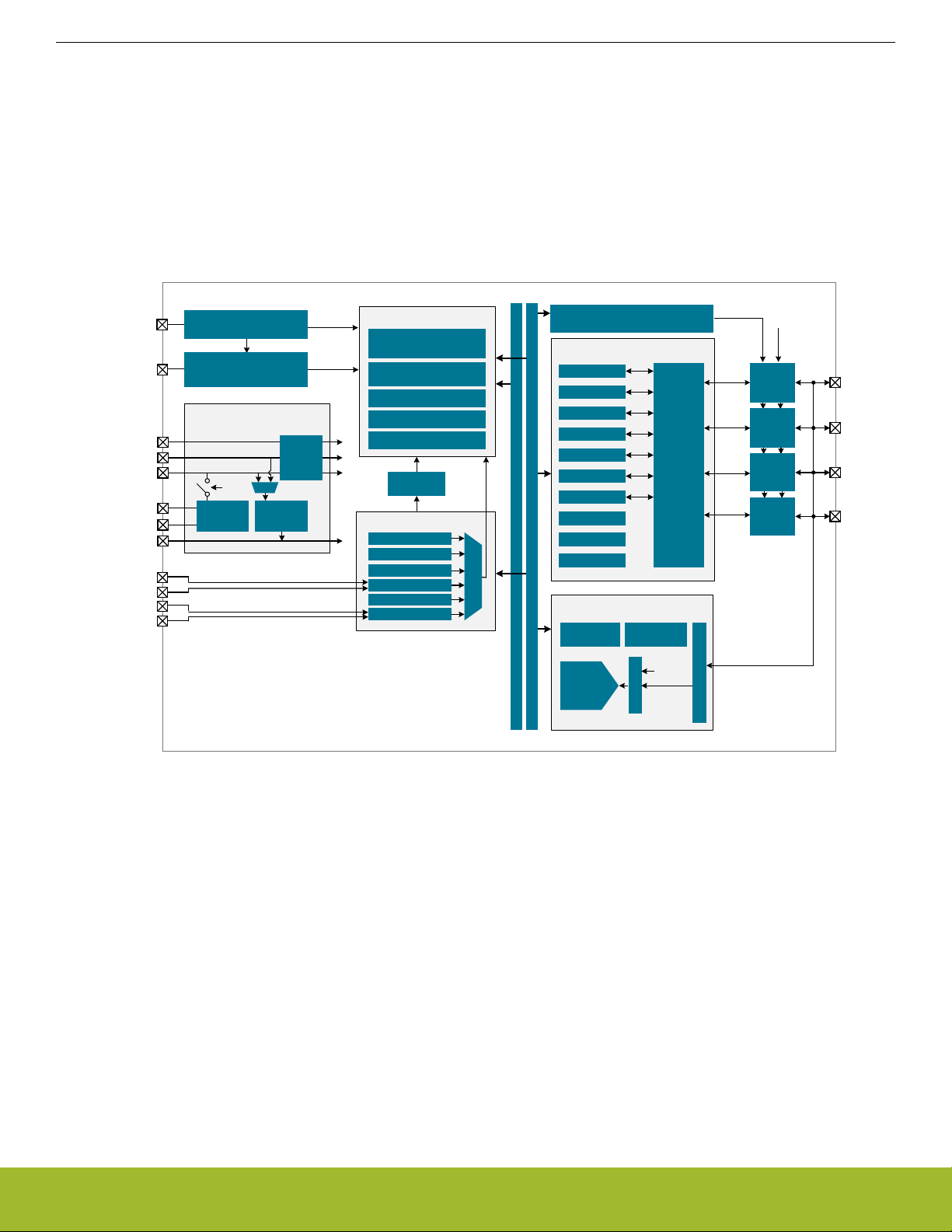
3. System Overview
3.1 Introduction
The EFM32PG22 Gecko product family is well suited for any battery operated application as well as other systems requiring high performance and low energy consumption. This section gives a short introduction to the MCU system. The detailed functional description
can be found in the EFM32PG22 Reference Manual.
A block diagram of the EFM32PG22 family is shown in Figure 3.1 Detailed EFM32PG22 Block Diagram on page 7. The diagram
shows a superset of features available on the family, which vary by OPN. For more information about specific device features, consult
Ordering Information.
RESETn
Debug Signals
(shared w/GPIO)
IOVDD
AVDD
DVDD
VREGVDD
VREGSW
DECOUPLE
LFXTAL_I
LFXTAL_O
HFXTAL_I
HFXTAL_O
Reset Management Unit,
Brown Out and POR
Serial Wire and ETM
Debug / Programming
with Debug Challenge I/F
Energy Management
Voltage
Monitor
bypass
DC-DC
Converter
Voltage
Regulator
Core and Memory
ARM Cortex-M33 Core
with Floating Point Unit
Up to 512 KB ISP Flash
Program Memory
32 KB RAM
Trust Zone
LDMA Controller
Watchdog
Timer
Clock Management
ULFRCO
FSRCO
LFRCO
LFXO
HFRCO
HFXO
Port I/O Configuration
IOVDD
Digital Peripherals
USART
EUART
I2C
LETIMER
TIMER
RTCC
A
A
H
P
B
B
PDM
TRNG
CRYPTOACC
CRC
DBUS
Port
Mappers
Port A
Drivers
Port B
Drivers
Port C
Drivers
Port D
Drivers
PAn
PBn
PCn
PDn
Analog Peripherals
Internal
Reference
12-16-bit
ADC
Temperature
Sensor
VDD
Input Mux
ABUS Multiplexers
Figure 3.1. Detailed EFM32PG22 Block Diagram
3.2 General Purpose Input/Output (GPIO)
EFM32PG22 has up to 26 General Purpose Input/Output pins. Each GPIO pin can be individually configured as either an output or
input. More advanced configurations including open-drain, open-source, and glitch-filtering can be configured for each individual GPIO
pin. The GPIO pins can be overridden by peripheral connections, like SPI communication. Each peripheral connection can be routed to
several GPIO pins on the device. The input value of a GPIO pin can be routed through the Peripheral Reflex System to other peripherals. The GPIO subsystem supports asynchronous external pin interrupts.
All of the pins on ports A and port B are EM2 capable. These pins may be used by Low-Energy peripherals in EM2/3 and may also be
used as EM2/3 pin wake-ups. Pins on ports C and D are latched/retained in their current state when entering EM2 until EM2 exit upon
which internal peripherals could once again drive those pads.
A few GPIOs also have EM4 wake functionality. These pins are listed in the Alternate Function Table.
silabs.com | Building a more connected world. Rev. 1.0 | 7
Page 8

EFM32PG22 Gecko MCU Family Data Sheet
System Overview
3.3 Clocking
3.3.1 Clock Management Unit (CMU)
The Clock Management Unit controls oscillators and clocks in the EFM32PG22. Individual enabling and disabling of clocks to all peripheral modules is performed by the CMU. The CMU also controls enabling and configuration of the oscillators. A high degree of flexibility
allows software to optimize energy consumption in any specific application by minimizing power dissipation in unused peripherals and
oscillators.
3.3.2 Internal and External Oscillators
The EFM32PG22 supports two crystal oscillators and fully integrates four RC oscillators, listed below.
• A high frequency crystal oscillator (HFXO) with integrated load capacitors, tunable in small steps, provides a precise timing reference for the MCU. The HFXO can also support an external clock source such as a TCXO for applications that require an extremely
accurate clock frequency over temperature.
• A 32.768 kHz crystal oscillator (LFXO) provides an accurate timing reference for low energy modes.
• An integrated high frequency RC oscillator (HFRCO) is available for the MCU system, when crystal accuracy is not required. The
HFRCO employs fast start-up at minimal energy consumption combined with a wide frequency range, from 1 MHz to 76.8 MHz.
• An integrated fast start-up RC oscillator (FSRCO) that runs at a fixed 20 MHz
• An integrated low frequency 32.768 kHz RC oscillator (LFRCO) for low power operation without an external crystal. Precision mode
enables periodic recalibration against the 38.4 MHz HFXO crystal to improve accuracy to +/- 500 ppm.
• An integrated ultra-low frequency 1 kHz RC oscillator (ULFRCO) is available to provide a timing reference at the lowest energy consumption in low energy modes.
3.4 Counters/Timers and PWM
3.4.1 Timer/Counter (TIMER)
TIMER peripherals keep track of timing, count events, generate PWM outputs and trigger timed actions in other peripherals through the
Peripheral Reflex System (PRS). The core of each TIMER is a 16-bit or 32-bit counter with up to 3 compare/capture channels. Each
channel is configurable in one of three modes. In capture mode, the counter state is stored in a buffer at a selected input event. In
compare mode, the channel output reflects the comparison of the counter to a programmed threshold value. In PWM mode, the TIMER
supports generation of pulse-width modulation (PWM) outputs of arbitrary waveforms defined by the sequence of values written to the
compare registers. In addition some timers offer dead-time insertion.
See 3.12 Configuration Summary for information on the feature set of each timer.
3.4.2 Low Energy Timer (LETIMER)
The unique LETIMER is a 24-bit timer that is available in energy mode EM0 Active, EM1 Sleep, EM2 Deep Sleep, and EM3 Stop. This
allows it to be used for timing and output generation when most of the device is powered down, allowing simple tasks to be performed
while the power consumption of the system is kept at an absolute minimum. The LETIMER can be used to output a variety of waveforms with minimal software intervention. The LETIMER is connected to the Peripheral Reflex System (PRS), and can be configured to
start counting on compare matches from other peripherals such as the Real Time Clock.
3.4.3 Real Time Clock with Capture (RTCC)
The Real Time Clock with Capture (RTCC) is a 32-bit counter providing timekeeping down to EM3. The RTCC can be clocked by any of
the on-board low-frequency oscillators, and it is capable of providing system wake-up at user defined intervals.
3.4.4 Back-Up Real Time Counter (BURTC)
The Back-Up Real Time Counter (BURTC) is a 32-bit counter providing timekeeping in all energy modes, including EM4. The BURTC
can be clocked by any of the on-board low-frequency oscillators, and it is capable of providing system wake-up at user defined invervals.
3.4.5 Watchdog Timer (WDOG)
The watchdog timer can act both as an independent watchdog or as a watchdog synchronous with the CPU clock. It has windowed
monitoring capabilities, and can generate a reset or different interrupts depending on the failure mode of the system. The watchdog can
also monitor autonomous systems driven by the Peripheral Reflex System (PRS).
silabs.com | Building a more connected world. Rev. 1.0 | 8
Page 9

EFM32PG22 Gecko MCU Family Data Sheet
System Overview
3.5 Communications and Other Digital Peripherals
3.5.1 Universal Synchronous/Asynchronous Receiver/Transmitter (USART)
The Universal Synchronous/Asynchronous Receiver/Transmitter is a flexible serial I/O module. It supports full duplex asynchronous
UART communication with hardware flow control as well as RS-485, SPI, MicroWire and 3-wire. It can also interface with devices supporting:
• ISO7816 SmartCards
• IrDA
•
I2S
3.5.2 Enhanced Universal Asynchronous Receiver/Transmitter (EUART)
The Enhanced Universal Asynchronous Receiver/Transmitter supports full duplex asynchronous UART communication with hardware
flow control, RS-485 and IrDA support. In EM0 and EM1 the EUART provides a high-speed, buffered communication interface.
When routed to GPIO ports A or B, the EUART may also be used in a low-energy mode and operate in EM2. A 32.768 kHz clock
source allows full duplex UART communication up to 9600 baud.
3.5.3 Inter-Integrated Circuit Interface (I2C)
The I2C module provides an interface between the MCU and a serial I2C bus. It is capable of acting as both a master and a slave and
supports multi-master buses. Standard-mode, fast-mode and fast-mode plus speeds are supported, allowing transmission rates from 10
kbit/s up to 1 Mbit/s. Slave arbitration and timeouts are also available, allowing implementation of an SMBus-compliant system. The
interface provided to software by the I2C module allows precise timing control of the transmission process and highly automated transfers. Automatic recognition of slave addresses is provided in active and low energy modes. Note that not all instances of I2C are avalia-
ble in all energy modes.
3.5.4 Peripheral Reflex System (PRS)
The Peripheral Reflex System provides a communication network between different peripheral modules without software involvement.
Peripheral modules producing Reflex signals are called producers. The PRS routes Reflex signals from producers to consumer peripherals which in turn perform actions in response. Edge triggers and other functionality such as simple logic operations (AND, OR, NOT)
can be applied by the PRS to the signals. The PRS allows peripherals to act autonomously without waking the MCU core, saving power.
3.5.5 Pulse Density Modulation (PDM) Interface
The PDM module provides a serial interface and decimation filter for Pulse Density Modulation (PDM) microphones, isolated Sigmadelta ADCs, digital sensors and other PDM or sigma delta bit stream peripherals. A programmable Cascaded Integrator Comb (CIC)
filter is used to decimate the incoming bit streams. PDM supports stereo or mono input data and DMA transfer.
3.6 Security Features
The following security features are available on the EFM32PG22:
• Secure Boot with Root of Trust and Secure Loader (RTSL)
• Cryptographic Accelerator
• True Random Number Generator (TRNG)
• Secure Debug with Lock/Unlock
3.6.1 Secure Boot with Root of Trust and Secure Loader (RTSL)
The Secure Boot with RTSL authenticates a chain of trusted firmware that begins from an immutable memory (ROM).
It prevents malware injection, prevents rollback, ensures that only authentic firmware is executed.
More information on this feature can be found in the Application Note AN1218: Series 2 Secure Boot with RTSL.
silabs.com | Building a more connected world. Rev. 1.0 | 9
Page 10

EFM32PG22 Gecko MCU Family Data Sheet
System Overview
3.6.2 Cryptographic Accelerator
The Cryptographic Accelerator is an autonomous hardware accelerator which supports AES encryption and decryption with
128/192/256-bit keys, Elliptic Curve Cryptography (ECC) to support public key operations and hashes.
Supported block cipher modes of operation for AES include:
• ECB (Electronic Code Book)
• CTR (Counter Mode)
• CBC (Cipher Block Chaining)
• CFB (Cipher Feedback)
• GCM (Galois Counter Mode)
• CBC-MAC (Cipher Block Chaining Message Authentication Code)
• GMAC (Galois Message Authentication Code)
• CCM (Counter with CBC-MAC)
The Cryptographic Accelerator accelerates Elliptical Curve Cryptography and supports the NIST (National Institute of Standards and
Technology) recommended curves including P-192 and P-256 for ECDH(Elliptic Curve Diffie-Hellman) key derivation and ECDSA (Elliptic Curve Digital Signature Algorithm) sign and verify operations.
Supported hashes include SHA-1, SHA2/224, and SHA-2/256.
This implementation provides a fast and energy efficient solution to state of the art cryptographic needs.
3.6.3 True Random Number Generator
The True Random Number Generator module is a non-deterministic random number generator that harvests entropy from a thermal
energy source. It includes start-up health tests for the entropy source as required by NIST SP800-90B and AIS-31 as well as online
health tests required for NIST SP800-90C.
The TRNG is suitable for periodically generating entropy to seed an approved pseudo random number generator.
3.6.4 Secure Debug with Lock/Unlock
For obvious security reasons, it is critical for a product to have its debug interface locked before being released in the field.
In addition, the EFM32PG22 also provides a secure debug unlock function that allows authenticated access based on public key cryptography. This functionality is particularly useful for supporting failure analysis while maintaining confidentiality of IP and sensitive enduser data.
More information on this feature can be found in the Application Note AN1190.
3.7 Analog
3.7.1 Analog to Digital Converter (IADC)
The IADC is a hybrid architecture combining techniques from both SAR and Delta-Sigma style converters. It has a resolution of 12 bits
at 1 Msps and 16 bits at up to 76.9 ksps. Hardware oversampling reduces system-level noise over multiple front-end samples. The
IADC includes integrated voltage reference options. Inputs are selectable from a wide range of sources, including pins configurable as
either single-ended or differential.
silabs.com | Building a more connected world. Rev. 1.0 | 10
Page 11
EFM32PG22 Gecko MCU Family Data Sheet
System Overview
3.8 Power
The EFM32PG22 has an Energy Management Unit (EMU) and efficient integrated regulators to generate internal supply voltages. Only
a single external supply voltage is required, from which all internal voltages are created. An optional integrated DC-DC buck regulator
can be utilized to further reduce the current consumption. The DC-DC regulator requires one external inductor and one external capacitor.
The EFM32PG22 device family includes support for internal supply voltage scaling, as well as two different power domains groups for
peripherals. These enhancements allow for further supply current reductions and lower overall power consumption.
3.8.1 Energy Management Unit (EMU)
The Energy Management Unit manages transitions of energy modes in the device. Each energy mode defines which peripherals and
features are available and the amount of current the device consumes. The EMU can also be used to implement system-wide voltage
scaling and turn off the power to unused RAM blocks to optimize the energy consumption in the target application. The DC-DC regulator operation is tightly integrated with the EMU.
3.8.2 Voltage Scaling
The EFM32PG22 supports supply voltage scaling for the LDO powering DECOUPLE, with independent selections for EM0 / EM1 and
EM2 / EM3. Voltage scaling helps to optimize the energy efficiency of the system by operating at lower voltages when possible. The
default EM0 / EM1 voltage scaling level is VSCALE2, which allows the core to operate in active mode at full speed. The intermediate
level, VSCALE1, allows operation in EM0 and EM1 at up to 40 MHz. The lowest level, VSCALE0, can be used to conserve power in
EM2 and EM3. The EMU will automatically switch the target voltage scaling level when transitioning between energy modes.
3.8.3 DC-DC Converter
The DC-DC buck converter covers a wide range of load currents, provides high efficiency in energy modes EM0, EM1, EM2 and EM3,
and can supply up to 60 mA for device operation. An on-chip supply-monitor signals when the supply voltage is low to allow bypass of
the regulator via programmable software interrupt. It employs soft switching at boot and DCDC regulating-to-bypass transitions to limit
the max supply slew-rate and mitigate inrush current.
3.8.4 Power Domains
The EFM32PG22 has three peripheral power domains for operation in EM2 and EM3, as well as the ability to selectively retain configurations for EM0/EM1 peripherals. A small set of peripherals always remain powered on in EM2 and EM3, including all peripherals which
are available in EM4. If all of the peripherals in PD0B or PD0C are configured as unused, that power domain will be powered off in EM2
or EM3, reducing the overall current consumption of the device. Likewise, if the application can tolerate the setup time to re-configure
used EM0/EM1 peripherals on wake, register retention for these peripherals can be disabled to further reduce the EM2 or EM3 current.
Table 3.1. Peripheral Power Subdomains
Always available in EM2/EM3 Power Domain PD0B Power Domain PD0C
RTCC LETIMER0 LFRCO (Precision Mode)
LFRCO (Non-precision mode)
1
LFXO
BURTC
ULFRCO
1
1
1
IADC0
I2C0
WDOG0
EUART0
FSRCO PRS
DEBUG
Note:
1. Peripheral also available in EM4.
silabs.com | Building a more connected world. Rev. 1.0 | 11
Page 12

EFM32PG22 Gecko MCU Family Data Sheet
System Overview
3.9 Reset Management Unit (RMU)
The RMU is responsible for handling reset of the EFM32PG22. A wide range of reset sources are available, including several power
supply monitors, pin reset, software controlled reset, core lockup reset, and watchdog reset.
3.10 Core and Memory
3.10.1 Processor Core
The ARM Cortex-M processor includes a 32-bit RISC processor integrating the following features and tasks in the system:
• ARM Cortex-M33 RISC processor achieving 1.50 Dhrystone MIPS/MHz
• ARM TrustZone security technology
• Embedded Trace Macrocell (ETM) for real-time trace and debug
• Up to 512 kB flash program memory
• Up to 32 kB RAM data memory
• Configuration and event handling of all modules
• 2-pin Serial-Wire debug interface
3.10.2 Memory System Controller (MSC)
The Memory System Controller (MSC) is the program memory unit of the microcontroller. The flash memory is readable and writable
from both the Cortex-M and DMA. In addition to the main flash array where Program code is normally written the MSC also provides an
Information block where additional information such as special user information or flash-lock bits are stored. There is also a read-only
page in the information block containing system and device calibration data. Read and write operations are supported in energy modes
EM0 Active and EM1 Sleep.
3.10.3 Linked Direct Memory Access Controller (LDMA)
The Linked Direct Memory Access (LDMA) controller allows the system to perform memory operations independently of software. This
reduces both energy consumption and software workload. The LDMA allows operations to be linked together and staged, enabling sophisticated operations to be implemented.
silabs.com | Building a more connected world. Rev. 1.0 | 12
Page 13
EFM32PG22 Gecko MCU Family Data Sheet
System Overview
3.11 Memory Map
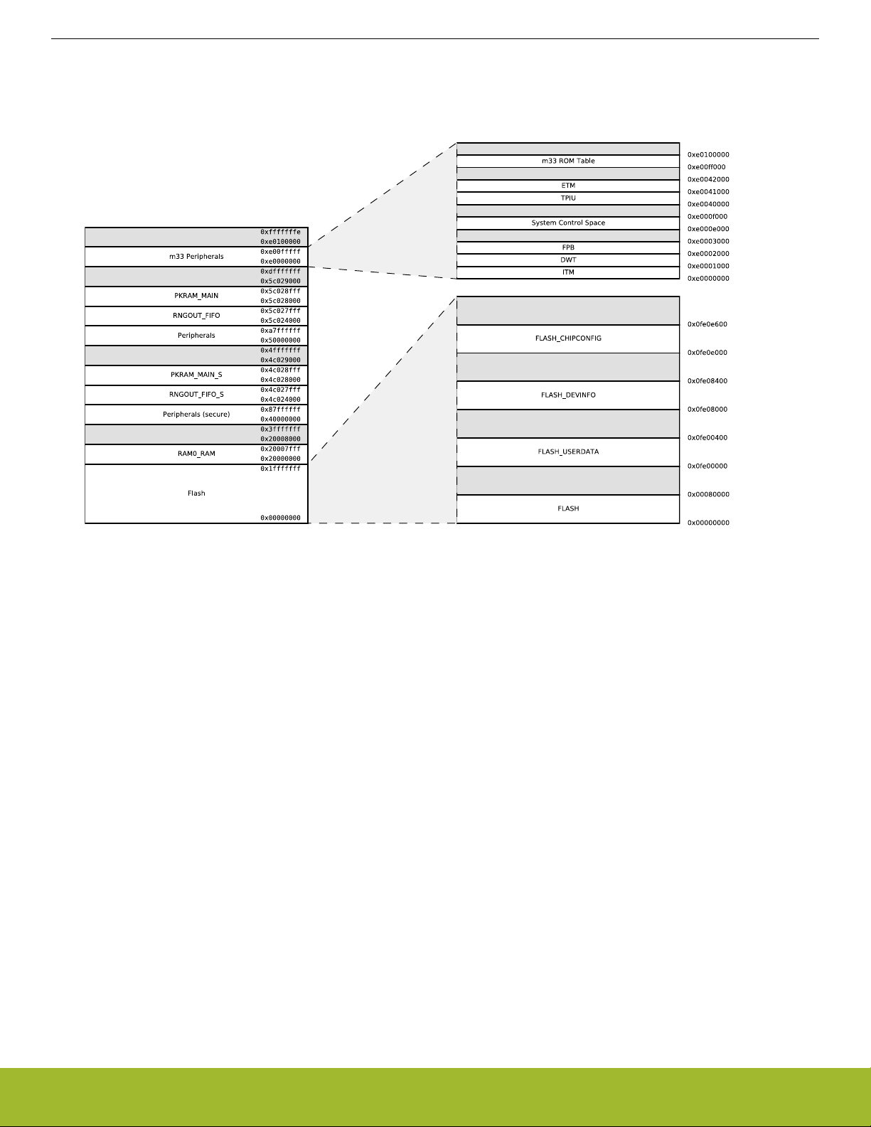
The EFM32PG22 memory map is shown in the figures below. RAM and flash sizes are for the largest memory configuration.
Figure 3.2. EFM32PG22 Memory Map — Core Peripherals and Code Space
silabs.com | Building a more connected world. Rev. 1.0 | 13
Page 14
EFM32PG22 Gecko MCU Family Data Sheet
System Overview
3.12 Configuration Summary
The features of the EFM32PG22 are a subset of the feature set described in the device reference manual. The table below describes
device specific implementation of the features. Remaining modules support full configuration.
Table 3.2. Configuration Summary
Module Lowest Energy Mode Configuration
I2C0
I2C1 EM1
IADC0 EM2
LETIMER0
PDM EM1 2-channel
TIMER0 EM1 32-bit, 3-channels, +DTI
TIMER1 EM1 16-bit, 3-channels, +DTI
TIMER2 EM1 16-bit, 3-channels, +DTI
TIMER3 EM1 16-bit, 3-channels, +DTI
EM2
EM2
1
1
TIMER4 EM1 16-bit, 3-channels, +DTI
EUART0 EM1 - Full high-speed operation
EM21 - Low-energy operation, 9600 Baud
USART0 EM1 +IrDA, +I2S, +SmartCard
USART1 EM1 +IrDA, +I2S, +SmartCard
Note:
1. EM2 and EM3 operation is only supported for digital peripheral I/O on Port A and Port B. All GPIO ports support digital peripheral
operation in EM0 and EM1.
silabs.com | Building a more connected world. Rev. 1.0 | 14
Page 15

EFM32PG22 Gecko MCU Family Data Sheet
Electrical Specifications
4. Electrical Specifications
4.1 Electrical Characteristics
All electrical parameters in all tables are specified under the following conditions, unless stated otherwise:
• Typical values are based on TA=25 °C and all supplies at 3.0 V, by production test and/or technology characterization.
• Minimum and maximum values represent the worst conditions across supply voltage, process variation, and operating temperature,
unless stated otherwise.
Power Supply Pin Dependencies
Due to on-chip circuitry (e.g., diodes), some EFM32 power supply pins have a dependent relationship with one or more other power
supply pins. These internal relationships between the external voltages applied to the various EFM32 supply pins are defined below.
Exceeding the below constraints can result in damage to the device and/or increased current draw.
• VREGVDD & DVDD
• In systems using the DCDC converter, DVDD (the buck converter output) should be connected to the recommended L
C
, and should not be driven by an off-chip regulator.
DCDC
• In systems not using the DCDC converter, DVDD must be shorted to VREGVDD on the PCB (VREGVDD=DVDD)
• DVDD ≥ DECOUPLE
• AVDD, IOVDD: No dependency with each other or any other supply pin
DCDC
and
silabs.com | Building a more connected world. Rev. 1.0 | 15
Page 16
EFM32PG22 Gecko MCU Family Data Sheet
Electrical Specifications
4.2 Absolute Maximum Ratings
Stresses beyond those listed below may cause permanent damage to the device. This is a stress rating only and functional operation of
the devices at those or any other conditions beyond those indicated in the operation listings of this specification is not implied. Exposure
to maximum rating conditions for extended periods may affect device reliability. For more information on the available quality and reliability data, see the Quality and Reliability Monitor Report at http://www.silabs.com/support/quality/pages/default.aspx.
Table 4.1. Absolute Maximum Ratings
Parameter Symbol Test Condition Min Typ Max Unit
Storage temperature range T
Voltage on any supply pin
1
Junction temperature T
Voltage ramp rate on any
supply pin
Voltage on HFXO pins V
DC voltage on any GPIO pin V
DC voltage on RESETn pin
2
Total current into VDD power
lines
Total current into VSS
ground lines
Current per I/O pin I
Current for all I/O pins I
STG
V
DDMAX
JMAX
V
DDRAMPMAX
HFXOPIN
DIGPIN
V
RESETn
I
VDDMAX
I
VSSMAX
IOMAX
IOALLMAX
-50 — +150 °C
-0.3 — 3.8 V
-I grade — — +125 °C
— — 1.0 V / µs
-0.3 — 1.4 V
-0.3 — V
IOVDD
+
V
0.3
-0.3 — 3.8 V
Source — — 200 mA
Sink — — 200 mA
Sink — — 50 mA
Source — — 50 mA
Sink — — 200 mA
Source — — 200 mA
Note:
1. The maximum supply voltage on VREGVDD is limited under certain conditions when using the DC-DC. See the DC-DC specifications for more details.
2. The RESETn pin has a pull-up device to the DVDD supply. For minimum leakage, RESETn should not exceed the voltage at
DVDD.
silabs.com | Building a more connected world. Rev. 1.0 | 16
Page 17
EFM32PG22 Gecko MCU Family Data Sheet
Electrical Specifications
4.3 General Operating Conditions
Table 4.2. General Operating Conditions
Parameter Symbol Test Condition Min Typ Max Unit
Operating ambient temperature range
T
A
-I temperature grade
1
-40 — +125 ° C
DVDD supply voltage V
AVDD supply voltage V
IOVDDx operating supply
voltage (All IOVDD pins)
VREGVDD operating supply
voltage
DECOUPLE output capaci-
4
tor
HCLK and SYSCLK frequen-cyf
PCLK frequency f
EM01 Group A clock frequency
DVDD
AVDD
V
IOVDDx
V
VREGVDD
C
DECOUPLE
HCLK
PCLK
f
EM01GRPACLK
EM0/1 1.71 3.0 3.8 V
EM2/3/4
2
1.71 3.0 3.8 V
1.71 3.0 3.8 V
1.71 3.0 3.8 V
DC-DC in regulation
3
2.2 3.0 3.8 V
DC-DC in bypass 60 mA load 1.8 3.0 3.8 V
DC-DC not in use. DVDD exter-
1.71 3.0 3.8 V
nally shorted to VREGVDD
1.0 µF ± 10% X8L capacitor used
1.0 — 2.75 µF
for performance characterization.
VSCALE2, MODE = WS1 — — 76.8 MHz
VSCALE2, MODE = WS0 — — 40 MHz
VSCALE2 — — 50 MHz
VSCALE1 — — 40 MHz
VSCALE2 — — 76.8 MHz
VSCALE1 — — 40 MHz
EM01 Group B clock frequency
f
EM01GRPBCLK
VSCALE2 — — 76.8 MHz
VSCALE1 — — 40 MHz
Note:
1. The device may operate continuously at the maximum allowable ambient TA rating as long as the absolute maximum T
JMAX
exceeded. For an application with significant power dissipation, the allowable TA may be lower than the maximum TA rating. TA =
T
- (THETAJA x PowerDissipation). Refer to the Absolute Maximum Ratings table and the Thermal Characteristics table for
JMAX
T
and THETAJA.
JMAX
2. The DVDD supply is monitored by the DVDD BOD in EM0/1 and the LE DVDD BOD in EM2/3/4.
3. The maximum supply voltage on VREGVDD is limited under certain conditions when using the DC-DC. See the DC-DC specifications for more details.
4. Murata GCM21BL81C105KA58L used for performance characterization. Actual capacitor values can be significantly de-rated
from their specified nominal value by the rated tolerance, as well as the application's AC voltage, DC bias, and temperature. The
minimum capacitance counting all error sources should be no less than 0.6 µF.
is not
silabs.com | Building a more connected world. Rev. 1.0 | 17
Page 18
4.4 DC-DC Converter
EFM32PG22 Gecko MCU Family Data Sheet
Electrical Specifications
Test conditions: L
V
= 1.8 V, IPKVAL in EM0/1 modes is set to 150 mA, and in EM2/3 modes is set to 90 mA, unless otherwise indicated.
OUT
= 2.2 µH (Samsung CIG22H2R2MNE), C
DCDC
= 4.7 µF (Samsung CL10B475KQ8NQNC), V
DCDC
VREGVDD
= 3.0 V,
Table 4.3. DC-DC Converter
Parameter Symbol Test Condition Min Typ Max Unit
Input voltage range at
VREGVDD pin
1
V
VREGVDD
DCDC in regulation, I
mA, EM0/EM1 mode
DCDC in regulation, I
LOAD
LOAD
= 60
= 5
2.2 3.0 3.8* V
1.8 3.0 3.8* V
mA, EM0/EM1 or EM2/EM3 mode
Bypass mode 1.8 3.0 3.8 V
Regulated output voltage V
OUT
Regulation DC accuracy ACC
DC
V
VREGVDD
≥ 2.2 V, Steady state in
— 1.8 — V
-2.5 — 3.3 %
EM0/EM1 mode or EM2/EM3
mode
Regulation total accuracy ACC
TOT
With mode transitions between
-5 — 7 %
EM0/EM1 and EM2/EM3 modes
Steady-state output ripple V
DC line regulation V
R
REG
I
= 20 mA in EM0/EM1 mode — 14.3 — mVpp
LOAD
I
= 60 mA in EM0/EM1
LOAD
mode, V
VREGVDD
≥ 2.2 V
— 5.5 — mV/V
DC load regulation I
REG
Load current between 100 µA and
60 mA in EM0/EM1 mode
Efficiency EFF Load current between 100 µA and
60 mA in EM0/EM1 mode, or between 10 µA and 5 mA in
EM2/EM3 mode
Output load current I
LOAD
EM0/EM1 mode, DCDC in regulation
EM2/EM3 mode, DCDC in regulation
Bypass mode — — 60 mA
Nominal output capacitor C
DCDC
4.7 µF ± 10% X7R capacitor used
for performance characterization
Nominal inductor L
Nominal input capacitor C
Resistance in bypass mode R
DCDC
IN
BYP
± 20% tolerance — 2.2 — µH
Bypass switch from VREGVDD to
DVDD, V
VREGVDD
= 1.8 V
Powertrain PFET switch from
VREGVDD to VREGSW,
V
VREGVDD
= 1.8 V
— 0.27 — mV/mA
— 91 — %
— — 60 mA
— — 5 mA
4.7 — 10 µF
2
C
DCDC
— — µF
— 1.75 3 Ω
— 0.86 1.5 Ω
Supply monitor threshold
V
CMP_RNG
Programmable in 0.1 V steps 2.0 — 2.3 V
programming range
Supply monitor threshold ac-
V
CMP_ACC
Supply falling edge trip point -5 — 5 %
curacy
silabs.com | Building a more connected world. Rev. 1.0 | 18
Page 19

EFM32PG22 Gecko MCU Family Data Sheet
Electrical Specifications
Parameter Symbol Test Condition Min Typ Max Unit
Supply monitor threshold
hysteresis
V
CMP_HYST
Positive hysteresis on the supply
rising edge referred to the falling
— 4 — %
edge trip point
Supply monitor response
time
t
CMP_DELAY
Supply falling edge at -100 mV /
µs
— 0.6 — µs
Note:
1. The supported maximum V
VREGVDD
in regulation mode is a function of temperature and 10-year lifetime average load current.
See more details in 4.4.1 DC-DC Operating Limits.
2. Samsung CL10B475KQ8NQNC used for performance characterization. Actual capacitor values can be significantly de-rated from
their specified nominal value by the rated tolerance, as well as the application's AC voltage, DC bias, and temperature. The minimum capacitance counting all error sources should be no less than 2.4 µF.
silabs.com | Building a more connected world. Rev. 1.0 | 19
Page 20
EFM32PG22 Gecko MCU Family Data Sheet
Electrical Specifications
4.4.1 DC-DC Operating Limits
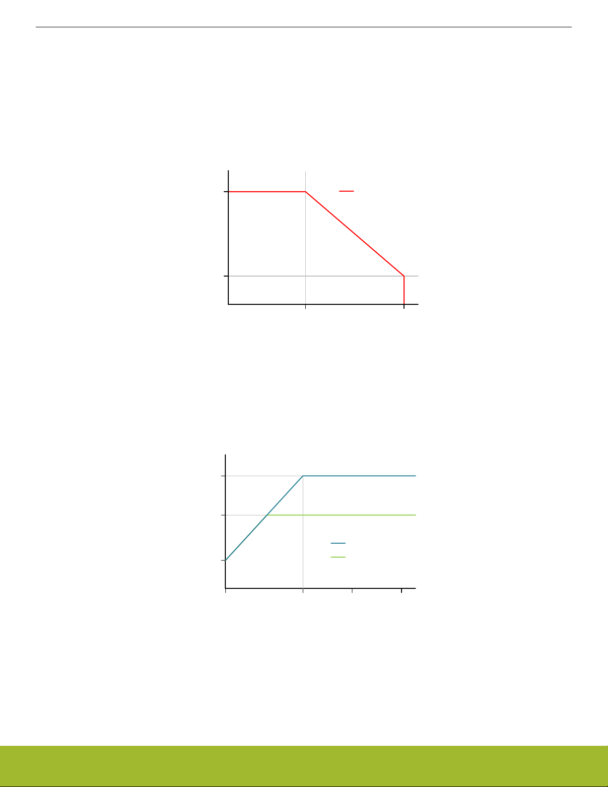
The maximum supported voltage on the VREGVDD supply pin is limited under certain conditions. Maximum input voltage is a function
of temperature and the average load current over a 10-year lifetime. Figure 4.1 Lifetime average load current limit vs. Maximum input
voltage on page 20 shows the safe operating region under specific conditions. Exceeding this safe operating range may impact the
reliability and performance of the DC-DC converter.
The average load current for an application can typically be determined by examining the current profile during the time the device is
powered. For example, an application that is continuously powered which spends 99% of the time asleep consuming 2 µA and 1% of
the time active and consuming 10 mA has an average lifetime load current of about 102 µA.
60
(mA)
LOAD
Tj ≤ 125 °C
5
Average Lifetime I
3.3 3.8
Maximum V
Figure 4.1. Lifetime average load current limit vs. Maximum input voltage
The minimum input voltage for the DC-DC in EM0/EM1 mode is a function of the maximum load current, and the peak current setting.
Figure 4.2 Transient maximum load current vs. Minimum input voltage on page 20 shows the max load current vs. input voltage for
different DC-DC peak inductor current settings.
VREGVDD
(V)
60
(mA)
36
LOAD
= 150 mA
I
PEAK
= 90 mA
I
VREGVDD
PEAK
(V)
5
Maximum I
1.8
2.2
Minimum V
Figure 4.2. Transient maximum load current vs. Minimum input voltage
silabs.com | Building a more connected world. Rev. 1.0 | 20
Page 21

EFM32PG22 Gecko MCU Family Data Sheet
Electrical Specifications
4.5 Thermal Characteristics
Table 4.4. Thermal Characteristics
Parameter Symbol Test Condition Min Typ Max Unit
Thermal Resistance Junction
to Ambient QFN32 (4x4mm)
THETA
JA_QFN32_4X4
4-Layer PCB, Natural Convection
Package
Thermal Resistance, Junction to Ambient, QFN40
THETA
JA_QFN40_5X5
4-Layer PCB, Natural Convection
(5x5mm) Package
Note:
1. Measured according to JEDEC standard JESD51-2A. Integrated Circuit Thermal Test Method Environmental Conditions - Natural
Convection (Still Air).
1
— 35.4 — °C/W
1
— 32.6 — °C/W
silabs.com | Building a more connected world. Rev. 1.0 | 21
Page 22
EFM32PG22 Gecko MCU Family Data Sheet
Electrical Specifications
4.6 Current Consumption
4.6.1 MCU current consumption using DC-DC at 3.0 V input
Unless otherwise indicated, typical conditions are: VREGVDD = 3.0 V. AVDD = DVDD = IOVDD = 1.8 V from DC-DC. Voltage scaling
level = VSCALE1. TA = 25 °C. Minimum and maximum values in this table represent the worst conditions across process variation at T
= 25 °C.
Table 4.5. MCU current consumption using DC-DC at 3.0 V input
Parameter Symbol Test Condition Min Typ Max Unit
A
Current consumption in EM0
mode with all peripherals disabled
I
ACTIVE
76.8 MHz HFRCO w/ DPLL referenced to 38.4 MHz crystal, CPU
running Prime from flash,
VSCALE2
76.8 MHz HFRCO w/ DPLL referenced to 38.4 MHz crystal, CPU
running while loop from flash,
VSCALE2
76.8 MHz HFRCO w/ DPLL referenced to 38.4 MHz crystal, CPU
running CoreMark loop from flash,
VSCALE2
38.4 MHz crystal, CPU running
Prime from flash
38.4 MHz crystal, CPU running
while loop from flash
38.4 MHz crystal, CPU running
CoreMark loop from flash
38 MHz HFRCO, CPU running
while loop from flash
26 MHz HFRCO, CPU running
while loop from flash
— 28 — µA/MHz
— 27 — µA/MHz
— 37 — µA/MHz
— 28 — µA/MHz
— 26 — µA/MHz
— 38 — µA/MHz
— 22 — µA/MHz
— 24 — µA/MHz
16 MHz HFRCO, CPU running
— 27 — µA/MHz
while loop from flash
1 MHz HFRCO, CPU running
— 159 — µA/MHz
while loop from flash
Current consumption in EM1
mode with all peripherals disabled
I
EM1
76.8 MHz HFRCO w/ DPLL referenced to 38.4 MHz crystal,
VSCALE2
— 17 — µA/MHz
38.4 MHz crystal — 17 — µA/MHz
38 MHz HFRCO — 13 — µA/MHz
26 MHz HFRCO — 15 — µA/MHz
16 MHz HFRCO — 18 — µA/MHz
1 MHz HFRCO — 150 — µA/MHz
silabs.com | Building a more connected world. Rev. 1.0 | 22
Page 23

EFM32PG22 Gecko MCU Family Data Sheet
Electrical Specifications
Parameter Symbol Test Condition Min Typ Max Unit
Current consumption in EM2
mode, VSCALE0
Current consumption in EM3
mode, VSCALE0
I
EM2_VS
I
EM3_VS
Full RAM retention and RTC running from LFXO
Full RAM retention and RTC running from LFRCO
Full RAM retention and RTC running from LFRCO in precision
mode
24 kB RAM retention and RTC
running from LFXO
24 kB RAM retention and RTC
running from LFRCO in precision
mode
8 kB RAM retention and RTC running from LFXO
8 kB RAM retention and RTC running from LFRCO
8 kB RAM retention and RTC running from LFXO, CPU cache not
retained
8 kB RAM retention and RTC running from ULFRCO
— 1.30 — µA
— 1.30 — µA
— 1.65 — µA
— 1.22 — µA
— 1.56 — µA
— 1.11 — µA
— 1.10 — µA
— 1.03 — µA
— 0.95 — µA
Additional current in EM2 or
I
PD0B_VS
— 0.37 — µA
EM3 when any peripheral in
PD0B is enabled
1
Note:
1. Extra current consumed by power domain. Does not include current associated with the enabled peripherals. See for a list of the
peripherals in each power domain.
silabs.com | Building a more connected world. Rev. 1.0 | 23
Page 24

EFM32PG22 Gecko MCU Family Data Sheet
Electrical Specifications
4.6.2 MCU current consumption at 3.0 V
Unless otherwise indicated, typical conditions are: AVDD = DVDD = IOVDD = VREGVDD = 3.0 V. DC-DC not used. Voltage scaling
level = VSCALE1. TA = 25 °C. Minimum and maximum values in this table represent the worst conditions across process variation at T
= 25 °C.
Table 4.6. MCU current consumption at 3.0 V
Parameter Symbol Test Condition Min Typ Max Unit
A
Current consumption in EM0
mode with all peripherals disabled
I
ACTIVE
76.8 MHz HFRCO w/ DPLL referenced to 38.4 MHz crystal, CPU
running Prime from flash,
VSCALE2
76.8 MHz HFRCO w/ DPLL referenced to 38.4 MHz crystal, CPU
running while loop from flash,
VSCALE2
76.8 MHz HFRCO w/ DPLL referenced to 38.4 MHz crystal, CPU
running CoreMark loop from flash,
VSCALE2
38.4 MHz crystal, CPU running
Prime from flash
38.4 MHz crystal, CPU running
while loop from flash
38.4 MHz crystal, CPU running
CoreMark loop from flash
38 MHz HFRCO, CPU running
while loop from flash
26 MHz HFRCO, CPU running
while loop from flash
— 42 — µA/MHz
— 39 — µA/MHz
— 54 — µA/MHz
— 40 — µA/MHz
— 39 — µA/MHz
— 55 — µA/MHz
— 33 50 µA/MHz
— 35 — µA/MHz
Current consumption in EM1
mode with all peripherals disabled
I
EM1
16 MHz HFRCO, CPU running
— 40 — µA/MHz
while loop from flash
1 MHz HFRCO, CPU running
— 228 830 µA/MHz
while loop from flash
76.8 MHz HFRCO w/ DPLL refer-
— 24 — µA/MHz
enced to 38.4 MHz crystal,
VSCALE2
38.4 MHz crystal — 25 — µA/MHz
38 MHz HFRCO — 19 35 µA/MHz
26 MHz HFRCO — 21 — µA/MHz
16 MHz HFRCO — 27 — µA/MHz
1 MHz HFRCO — 215 770 µA/MHz
silabs.com | Building a more connected world. Rev. 1.0 | 24
Page 25

EFM32PG22 Gecko MCU Family Data Sheet
Electrical Specifications
Parameter Symbol Test Condition Min Typ Max Unit
Current consumption in EM2
mode, VSCALE0
Current consumption in EM3
mode, VSCALE0
Current consumption in EM4
mode
I
EM2_VS
I
EM3_VS
I
EM4
Full RAM retention and RTC run-
— 1.74 — µA
ning from LFXO
Full RAM retention and RTC run-
— 1.75 4.9 µA
ning from LFRCO
24 kB RAM retention and RTC
— 1.61 — µA
running from LFXO
24 kB RAM retention and RTC
— 2.14 — µA
running from LFRCO in precision
mode
8 kB RAM retention and RTC run-
— 1.44 — µA
ning from LFXO
8 kB RAM retention and RTC run-
— 1.45 — µA
ning from LFRCO
8 kB RAM retention and RTC run-
— 1.39 — µA
ning from LFXO, CPU cache not
retained
8 kB RAM retention and RTC run-
— 1.21 3.7 µA
ning from ULFRCO
No BURTC, no LF oscillator — 0.17 0.43 µA
BURTC with LFXO — 0.50 — µA
Current consumption during
I
RST
Hard pin reset held — 234 — µA
reset
Additional current in EM2 or
I
PD0B_VS
— 0.56 — µA
EM3 when any peripheral in
PD0B is enabled
1
Note:
1. Extra current consumed by power domain. Does not include current associated with the enabled peripherals. See for a list of the
peripherals in each power domain.
silabs.com | Building a more connected world. Rev. 1.0 | 25
Page 26

EFM32PG22 Gecko MCU Family Data Sheet
Electrical Specifications
4.6.3 MCU current consumption at 1.8 V
Unless otherwise indicated, typical conditions are: AVDD = DVDD = IOVDD = VREGVDD = 1.8 V. DC-DC not used. Voltage scaling
level = VSCALE1. TA = 25 °C. Minimum and maximum values in this table represent the worst conditions across process variation at T
= 25 °C.
Table 4.7. MCU current consumption at 1.8 V
Parameter Symbol Test Condition Min Typ Max Unit
A
Current consumption in EM0
mode with all peripherals disabled
I
ACTIVE
76.8 MHz HFRCO w/ DPLL referenced to 38.4 MHz crystal, CPU
running Prime from flash,
VSCALE2
76.8 MHz HFRCO w/ DPLL referenced to 38.4 MHz crystal, CPU
running while loop from flash,
VSCALE2
76.8 MHz HFRCO w/ DPLL referenced to 38.4 MHz crystal, CPU
running CoreMark loop from flash,
VSCALE2
38.4 MHz crystal, CPU running
Prime from flash
38.4 MHz crystal, CPU running
while loop from flash
38.4 MHz crystal, CPU running
CoreMark loop from flash
38 MHz HFRCO, CPU running
while loop from flash
26 MHz HFRCO, CPU running
while loop from flash
— 42 — µA/MHz
— 39 — µA/MHz
— 54 — µA/MHz
— 41 — µA/MHz
— 39 — µA/MHz
— 55 — µA/MHz
— 33 — µA/MHz
— 35 — µA/MHz
Current consumption in EM1
mode with all peripherals disabled
I
EM1
16 MHz HFRCO, CPU running
— 40 — µA/MHz
while loop from flash
1 MHz HFRCO, CPU running
— 227 — µA/MHz
while loop from flash
76.8 MHz HFRCO w/ DPLL refer-
— 24 — µA/MHz
enced to 38.4 MHz crystal,
VSCALE2
38.4 MHz crystal — 25 — µA/MHz
38 MHz HFRCO — 19 — µA/MHz
26 MHz HFRCO — 21 — µA/MHz
16 MHz HFRCO — 27 — µA/MHz
1 MHz HFRCO — 213 — µA/MHz
silabs.com | Building a more connected world. Rev. 1.0 | 26
Page 27

EFM32PG22 Gecko MCU Family Data Sheet
Electrical Specifications
Parameter Symbol Test Condition Min Typ Max Unit
Current consumption in EM2
mode, VSCALE0
Current consumption in EM3
mode, VSCALE0
Current consumption in EM4
mode
I
EM2_VS
I
EM3_VS
I
EM4
Full RAM retention and RTC run-
— 1.67 — µA
ning from LFXO
Full RAM retention and RTC run-
— 1.66 — µA
ning from LFRCO
24 kB RAM retention and RTC
— 1.53 — µA
running from LFXO
24 kB RAM retention and RTC
— 2.06 — µA
running from LFRCO in precision
mode
8 kB RAM retention and RTC run-
— 1.37 — µA
ning from LFXO
8 kB RAM retention and RTC run-
— 1.36 — µA
ning from LFRCO
8 kB RAM retention and RTC run-
— 1.32 — µA
ning from LFXO, CPU cache not
retained
8 kB RAM retention and RTC run-
— 1.14 — µA
ning from ULFRCO
No BURTC, no LF oscillator — 0.13 — µA
BURTC with LFXO — 0.44 — µA
Current consumption during
I
RST
Hard pin reset held — 190 — µA
reset
Additional current in EM2 or
I
PD0B_VS
— 0.54 — µA
EM3 when any peripheral in
PD0B is enabled
1
Note:
1. Extra current consumed by power domain. Does not include current associated with the enabled peripherals. See for a list of the
peripherals in each power domain.
silabs.com | Building a more connected world. Rev. 1.0 | 27
Page 28

EFM32PG22 Gecko MCU Family Data Sheet
Electrical Specifications
4.7 Flash Characteristics
Table 4.8. Flash Characteristics
Parameter Symbol Test Condition Min Typ Max Unit
Flash Supply voltage during
V
FLASH
write or erase
Flash erase cycles before
1
failure
Flash data retention
1
Program Time t
EC
RET
PROG
FLASH
FLASH
10,000 — — cycles
one word (32-bits) 42.1 44 45.6 uSec
average per word over 128 words 10.3 10.9 11.3 uSec
Page Erase Time t
Mass Erase Time t
Program Current I
Page Erase Current I
Mass Erase Current I
PERASE
MERASE
PROG
PERASE
MERASE
Erases all of User Code area 11.7 13 14.3 ms
Page Erase — — 1.34 mA
Mass Erase — — 1.28 mA
Note:
1. Flash data retention information is published in the Quarterly Quality and Reliability Report.
1.71 — 3.8 V
10 — — years
11.4 12.9 14.4 ms
— — 1.45 mA
silabs.com | Building a more connected world. Rev. 1.0 | 28
Page 29

EFM32PG22 Gecko MCU Family Data Sheet
Electrical Specifications
4.8 Wake Up, Entry, and Exit times
Unless otherwise specified, these times are measured using the HFRCO at 19 MHz.
Table 4.9. Wake Up, Entry, and Exit times
Parameter Symbol Test Condition Min Typ Max Unit
WakeupTime from EM1 t
WakeupTime from EM2 t
WakupTime from EM3 t
WakeupTime from EM4 t
Entry time to EM1 t
Entry time to EM2 t
EM1_WU
EM2_WU
EM3_WU
EM4_WU
EM1_ENT
EM2_ENT
Code execution from flash — 3 — AHB
Clocks
Code execution from RAM — 1.42 — µs
Code execution from flash, No
— 13.22 — µs
Voltage Scaling
Code execution from RAM, No
— 5.15 — µs
Voltage Scaling
Voltage scaling up one level
1
Voltage scaling up two levels
Code execution from flash, No
2
— 37.89 — µs
— 50.56 — µs
— 13.21 — µs
Voltage Scaling
Code execution from RAM, No
— 5.15 — µs
Voltage Scaling
Voltage scaling up one level
Voltage scaling up two levels
1
2
— 37.90 — µs
— 50.55 — µs
Code execution from flash — 8.81 — ms
Code execution from flash — 1.29 — µs
Code execution from flash — 5.23 — µs
Entry time to EM3 t
Entry time to EM4 t
Voltage scaling in time in
3
EM0
EM3_ENT
EM4_ENT
t
SCALE
Code execution from flash — 5.23 — µs
Code execution from flash — 9.96 — µs
Up from VSCALE1 to VSCALE2 — 32 — µs
Down from VSCALE2 to
— 172 — µs
VSCALE1
Note:
1. Voltage scaling one level is between VSCALE0 and VSCALE1 or between VSCALE1 and VSCALE2.
2. Voltage scaling two levels is between VSCALE0 and VSCALE2.
3. During voltage scaling in EM0, RAM is inaccessible and processor will be halted until complete.
silabs.com | Building a more connected world. Rev. 1.0 | 29
Page 30

EFM32PG22 Gecko MCU Family Data Sheet
Electrical Specifications
4.9 Oscillators
4.9.1 High Frequency Crystal Oscillator
Unless otherwise indicated, typical conditions are: AVDD = DVDD = 3.0 V. TA = 25 °C. Minimum and maximum values in this table
represent the worst conditions across process variation, operating supply voltage range, and operating temperature range.
Table 4.10. High Frequency Crystal Oscillator
Parameter Symbol Test Condition Min Typ Max Unit
Crystal Frequency F
Supported crystal equivalent
HFXO
ESR
HFXO_38M4
38.4 MHz, CL = 10 pF
1
— 38.4 — MHz
— 40 60 Ω
series resistance (ESR)
Supported range of crystal
load capacitance
2
Supply Current I
Startup Time T
C
HFXO_LC
HFXO
STARTUP
38.4 MHz, ESR = 40 Ω — 10 — pF
— 415 — µA
38.4 MHz, ESR = 40 Ohm, CL =
— 160 — µs
10 pF
On-chip tuning cap step
3
size
SS
HFXO
— 0.04 — pF
Note:
1. The crystal should have a maximum ESR less than or equal to this maximum rating.
2. Total load capacitance as seen by the crystal.
3. The tuning step size is the effective step size when incrementing one of the tuning capacitors by one count. The step size for the
each of the indivdual tuning capacitors is twice this value.
silabs.com | Building a more connected world. Rev. 1.0 | 30
Page 31

EFM32PG22 Gecko MCU Family Data Sheet
Electrical Specifications
4.9.2 Low Frequency Crystal Oscillator
Table 4.11. Low Frequency Crystal Oscillator
Parameter Symbol Test Condition Min Typ Max Unit
Crystal Frequency F
Supported Crystal equivalent
series resistance (ESR)
Supported range of crystal
load capacitance
1
LFXO
ESR
C
LFXO_CL
LFXO
GAIN = 0 — — 80 kΩ
GAIN = 1 to 3 — — 100 kΩ
GAIN = 0 4 — 6 pF
GAIN = 1 6 — 10 pF
GAIN = 2 10 — 12.5 pF
GAIN = 3 (see note2)
Current consumption I
CL12p5
ESR = 70 kOhm, CL = 12.5 pF,
GAIN3 = 2, AGC4 = 1
Startup Time T
STARTUP
ESR = 70 kOhm, CL = 7 pF,
GAIN3 = 1, AGC4 = 1
On-chip tuning cap step size SS
On-chip tuning capacitor value at minimum setting
5
On-chip tuning capacitor value at maximum setting
5
LFXO
C
LFXO_MIN
C
LFXO_MAX
CAPTUNE = 0 — 4 — pF
CAPTUNE = 0x4F — 24.5 — pF
Note:
1. Total load capacitance seen by the crystal
2. Crystals with a load capacitance of greater than 12 pF require external load capacitors.
3. In LFXO_CAL Register
4. In LFXO_CFG Register
5. The effective load capacitance seen by the crystal will be C
/2. This is because each XTAL pin has a tuning cap and the two
LFXO
caps will be seen in series by the crystal
— 32.768 — kHz
12.5 — 18 pF
— 357 — nA
— 63 — ms
— 0.26 — pF
silabs.com | Building a more connected world. Rev. 1.0 | 31
Page 32

EFM32PG22 Gecko MCU Family Data Sheet
Electrical Specifications
4.9.3 High Frequency RC Oscillator (HFRCO)
Unless otherwise indicated, typical conditions are: AVDD = DVDD = 3.0 V. TA = 25 °C. Minimum and maximum values in this table
represent the worst conditions across process variation, operating supply voltage range, and operating temperature range.
Table 4.12. High Frequency RC Oscillator (HFRCO)
Parameter Symbol Test Condition Min Typ Max Unit
Frequency Accuracy F
Current consumption on all
supplies
1
HFRCO_ACC
I
HFRCO
For all production calibrated frequencies
F
F
F
F
F
F
F
F
F
F
F
F
F
F
= 1 MHz — 28 — µA
HFRCO
= 2 MHz — 28 — µA
HFRCO
= 4 MHz — 28 — µA
HFRCO
= 5 MHz — 30 — µA
HFRCO
= 7 MHz — 60 — µA
HFRCO
= 10 MHz — 66 — µA
HFRCO
= 13 MHz — 79 — µA
HFRCO
= 16 MHz — 88 — µA
HFRCO
= 19 MHz — 92 — µA
HFRCO
= 20 MHz — 105 — µA
HFRCO
= 26 MHz — 118 — µA
HFRCO
= 32 MHz — 141 — µA
HFRCO
= 38 MHz — 172 — µA
HFRCO
= 80 MHz — 289 — µA
HFRCO
-3 — 3 %
Clock out current for
HFRCODPLL
Startup Time
2
3
I
CLKOUT_HFRCOD
PLL
T
STARTUP
FORECEEN bit of CTRL = 1 and
— 2.72 — µA/MHz
the CLKOUTDIS0 bit of TEST = 1.
FORECEEN bit of CTRL i= 1 and
— 0.36 — µA/MHz
the CLKOUTDIS1 bit of TEST = 1.
FREQRANGE = 0 to 7 — 1.2 — µs
FREQRANGE = 8 to 15 — 0.6 — µs
silabs.com | Building a more connected world. Rev. 1.0 | 32
Page 33

EFM32PG22 Gecko MCU Family Data Sheet
Electrical Specifications
Parameter Symbol Test Condition Min Typ Max Unit
Band Frequency Limits
4
f
HFRCO_BAND
FREQRANGE = 0 3.71 — 5.24 MHz
FREQRANGE = 1 4.39 — 6.26 MHz
FREQRANGE = 2 5.25 — 7.55 MHz
FREQRANGE = 3 6.22 — 9.01 MHz
FREQRANGE = 4 7.88 — 11.6 MHz
FREQRANGE = 5 9.9 — 14.6 MHz
FREQRANGE = 6 11.5 — 17.0 MHz
FREQRANGE = 7 14.1 — 20.9 MHz
FREQRANGE = 8 16.4 — 24.7 MHz
FREQRANGE = 9 19.8 — 30.4 MHz
FREQRANGE = 10 22.7 — 34.9 MHz
FREQRANGE = 11 28.6 — 44.4 MHz
FREQRANGE = 12 33.0 — 51.0 MHz
FREQRANGE = 13 42.2 — 64.6 MHz
FREQRANGE = 14 48.8 — 74.8 MHz
FREQRANGE = 15 57.6 — 87.4 MHz
Note:
1. Does not include additional clock tree current. See specifications for additional current when selected as a clock source for a particular clock multiplexer.
2. When the HFRCO is enabled for characterization using the FORCEEN bit, the total current will be the HFRCO core current plus
the specified CLKOUT current. When the HFRCO is enabled on demand, the clock current may be different.
3. Hardware delay ensures settling to within ± 0.5%. Hardware also enforces this delay on a band change.
4. The frequency band limits represent the lowest and highest freqeuncy which each band can achieve over the operating range.
4.9.4 Fast Start_Up RC Oscillator (FSRCO)
Table 4.13. Fast Start_Up RC Oscillator (FSRCO)
Parameter Symbol Test Condition Min Typ Max Unit
FSRCO frequency F
FSRCO
17.2 20 21.2 MHz
silabs.com | Building a more connected world. Rev. 1.0 | 33
Page 34

EFM32PG22 Gecko MCU Family Data Sheet
Electrical Specifications
4.9.5 Low Frequency RC Oscillator (LFRCO)
Table 4.14. Low Frequency RC Oscillator (LFRCO)
Parameter Symbol Test Condition Min Typ Max Unit
Nominal oscillation frequen-cyF
Frequency accuracy F
Startup time t
Current consumption I
LFRCO
LFRCO_ACC
STARTUP
LFRCO
— 32.768 — kHz
-3 — 3 %
— 204 — µs
— 175 — nA
4.9.6 Ultra Low Frequency RC Oscillator
Table 4.15. Ultra Low Frequency RC Oscillator
Parameter Symbol Test Condition Min Typ Max Unit
Oscillation Frequency F
ULFRCO
0.944 1.0 1.095 kHz
silabs.com | Building a more connected world. Rev. 1.0 | 34
Page 35

EFM32PG22 Gecko MCU Family Data Sheet
Electrical Specifications
4.10 GPIO Pins (3V GPIO pins)
Table 4.16. GPIO Pins (3V GPIO pins)
Parameter Symbol Test Condition Min Typ Max Unit
Leakage current I
Input low voltage
Input high voltage
1
1
Hysteresis of input voltage V
Output high voltage V
LEAK_IO
V
IL
V
IH
HYS
OH
MODEx = DISABLED, IOVDD =
— 1.9 — nA
1.71 V
MODEx = DISABLED, IOVDD =
— 2.5 — nA
3.0 V
Pins other than PA00, PA03,
— — 200 nA
PB00, PC03, PC04 and PD00;
MODEx = DISABLED, IOVDD =
3.8 V TA = 125 °C
Pins PA00, PA03, PB00, PC03,
— — 550 nA
PC04 and PD00; MODEx = DISABLED, IOVDD = 3.8 V TA = 125
°C
Any GPIO pin — — 0.3*IOVDD V
RESETn — — 0.3*DVDD V
Any GPIO pin 0.7*IOVDD — — V
RESETn 0.7*DVDD — — V
Any GPIO pin 0.05*IOVD
— — V
D
RESETn 0.05*DVDD — — V
Sourcing 20mA, IOVDD = 3.0 V 0.8 *
— — V
IOVDD
Output low voltage V
GPIO rise time T
GPIO fall time T
Pull up/down resistance
2
OL
GPIO_RISE
GPIO_FALL
R
PULL
Sourcing 8mA, IOVDD = 1.71 V 0.6 *
— — V
IOVDD
Sinking 20mA, IOVDD = 3.0 V — — 0.2 *
V
IOVDD
Sinking 8mA, IOVDD = 1.71 V — — 0.4 *
V
IOVDD
IOVDD = 3.0 V, C
load
= 50pF,
— 8.4 — ns
SLEWRATE = 4, 10% to 90%
IOVDD = 1.71 V, C
load
= 50pF,
— 13 — ns
SLEWRATE = 4, 10% to 90%
IOVDD = 3.0 V, C
load
= 50pF,
— 7.1 — ns
SLEWRATE = 4, 90% to 10%
IOVDD = 1.71 V, C
load
= 50pF,
— 11.9 — ns
SLEWRATE = 4, 90% to 10%
Any GPIO pin. Pull-up to IOVDD:
35 44 55 kΩ
MODEn = DISABLE DOUT=1.
Pull-down to VSS: MODEn =
WIREDORPULLDOWN DOUT =
0.
RESETn pin. Pull-up to DVDD 35 44 55 kΩ
Maximum filtered glitch width T
silabs.com | Building a more connected world. Rev. 1.0 | 35
GF
MODE = INPUT, DOUT = 1 — 27 — ns
Page 36

EFM32PG22 Gecko MCU Family Data Sheet
Electrical Specifications
Parameter Symbol Test Condition Min Typ Max Unit
Note:
1. GPIO input thresholds are proportional to the IOVDD pin. RESETn input thresholds are proportional to DVDD.
2. GPIO pull-ups connect to IOVDD supply, pull-downs connect to VSS. RESETn pull-up connects to DVDD.
silabs.com | Building a more connected world. Rev. 1.0 | 36
Page 37

EFM32PG22 Gecko MCU Family Data Sheet
Electrical Specifications
4.11 Analog to Digital Converter (IADC)
Specified at 1 Msps, ADCCLK = 10 MHz, OSR=2, unless otherwise indicated.
Table 4.17. Analog to Digital Converter (IADC)
Parameter Symbol Test Condition Min Typ Max Unit
Main analog supply V
Maximum Input Range
1
Full-Scale Voltage V
AVDD
V
IN_MAX
FS
Normal Mode 1.71 — 3.8 V
Maximum allowable input voltage 0 — AVDD V
Voltage required for Full-Scale
— V
/ Gain —
REF
measurement
Input Measurement Range V
IN
Differential Mode - Plus and Mi-
-V
FS
— +V
FS
V
nus inputs
Single Ended Mode - One input
0 — V
FS
V
tied to ground
Input Sampling Capacitance Cs Analog Gain = 1x — 1.8 — pF
Analog Gain = 2x — 3.6 — pF
Analog Gain = 4x — 7.2 — pF
Analog Gain = 0.5x — 0.9 — pF
ADC clock frequency f
Throughput rate f
Current from all supplies,
Continuous operation
CLK
SAMPLE
I
ADC_CONT
Normal Mode — — 10 MHz
f
= 10 MHz, OSR = 2 — — 1 Msps
CLK
f
= 10 MHz, OSR = 32 — — 76.9 ksps
CLK
Normal Mode, 1 Msps, OSR = 2,
f
= 10 MHz
CLK
— 290 385 µA
Current in Standby mode.
I
STBY
Normal Mode — 16 — µA
ADC is not functional but can
wake up in 1us.
ADC Startup Time t
startup
From power down state — 5 — µs
From Standby state — 1 — µs
ADC Resolution
2
Resolution — 12 — bits
Differential Nonlinearity DNL Differential Input, OSR = 2, (No
missing codes) .
Integral Nonlinearity INL Normal Mode, Differential Input,
OSR = 2.
3
Effective number of bits
ENOB Differential Input. Gain = 1x, OSR
= 2, fIN = 10 kHz, Internal
VREF=1.21V. OSR=2
Differential Input. Gain = 1x, OSR
= 32, fIN = 2.5 kHz, Internal VREF
= 1.21 V.
Differential Input. Gain = 1x, OSR
= 32, fIN = 2.5 kHz, External
VREF = 1.25 V.
-1 +/- 0.25 1.5 LSB12
-2.5 +/- 0.65 2.5 LSB12
10.5 11.7 — bits
— 13.5 — bits
— 14.3 — bits
silabs.com | Building a more connected world. Rev. 1.0 | 37
Page 38

EFM32PG22 Gecko MCU Family Data Sheet
Electrical Specifications
Parameter Symbol Test Condition Min Typ Max Unit
Signal to Noise + Distortion
3
Ratio
SNDR Differential Input. Gain=1x, OSR =
2, fIN = 10 kHz, Internal
VREF=1.21V
Differential Input. Gain=2x, OSR =
2, fIN = 10 kHz, Internal
VREF=1.21V
Differential Input. Gain=4x, OSR =
2, fIN = 10 kHz, Internal
VREF=1.21V
Differential Input. Gain=0.5x, OSR
= 2, fIN = 10 kHz, Internal
VREF=1.21V
Total Harmonic Distortion THD Differential Input. Gain=1x, OSR =
2, fIN = 10 kHz, Internal
VREF=1.21V
Spurious-Free Dynamic
Range
SFDR Differential Input. Gain=1x, OSR =
2, fIN = 10 kHz, Internal
VREF=1.21V
Common Mode Rejection
Ratio
Power Supply Rejection Ratio
CMRR Normal Mode. DC to 100 Hz — 87.0 — dB
Normal Mode. AC high frequency — 68.6 — dB
PSRR Normal mode. DC to 100 Hz — 80.4 — dB
Normal mode. AC high frequency,
using VREF pad.
65 72.3 — dB
— 72.3 — dB
— 68.8 — dB
— 72.5 — dB
— -80.8 -70 dB
72 86.5 — dB
— 33.4 — dB
Normal mode. AC high frequency,
— 65.2 — dB
using internal VBGR.
Gain Error GE GAIN=1 and 0.5, using external
-0.3 0.069 0.3 %
VREF, direct mode.
GAIN=2, using external VREF, di-
-0.4 0.151 0.4 %
rect mode.
GAIN=3, using external VREF, di-
-0.7 0.186 0.7 %
rect mode.
GAIN=4, using external VREF, di-
-1.1 0.227 1.1 %
rect mode.
Internal VREF4, all GAIN settings
-1.5 0.023 1.5 %
Offset OFFSET GAIN=1 and 0.5, Differential Input -3 0.27 3 LSB
GAIN=2, Differential Input -4 0.27 4 LSB
GAIN=3, Differential Input -4 0.25 4 LSB
GAIN=4, Differential Input -4 0.29 4 LSB
External reference voltage
1
range
Internal Reference voltage V
V
EVREF
IVREF
1.0 — AVDD V
— 1.21 — V
silabs.com | Building a more connected world. Rev. 1.0 | 38
Page 39

EFM32PG22 Gecko MCU Family Data Sheet
Electrical Specifications
Parameter Symbol Test Condition Min Typ Max Unit
Note:
1. When inputs are routed to external GPIO pins, the maximum pin voltage is limited to the lower of the IOVDD and AVDD supplies.
2. ADC output resolution depends on the OSR and digital averaging settings. With no digital averaging, ADC output resolution is 12
bits at OSR=2, 13 bits at OSR = 4, 14 bits at OSR = 8, 15 bits at OSR = 16, 16 bits at OSR = 32 and 17 bits at OSR = 64. Digital
averaging has a similar impact on ADC output resolution. See the product reference manual for additional details.
3. The relationship between ENOB and SNDR is specified according to the equation: ENOB = (SNDR - 1.76) / 6.02.
4. Includes error from internal VREF drift.
4.12 Temperature Sense
Table 4.18. Temperature Sense
Parameter Symbol Test Condition Min Typ Max Unit
1
Temperature sensor range
T
RANGE
-40 — 125 °C
Temperature sensor resolu-
T
RESOLUTION
— 0.25 — °C
tion
Measurement noise (RMS) T
NOISE
Single measurement — 0.6 — °C
16-sample average (TEMPAVG-
— 0.17 — °C
NUM = 0)
64-sample average (TEMPAVG-
— 0.12 — °C
NUM = 1)
Temperature offset T
OFF
Mean error of uncorrected output
— 3.14 — °C
across full temperature range
Temperature sensor accura-
3
cy2
T
ACC
Direct output accuracy after mean
error (T
) removed
OFF
After linearization in software, no
-3 — 3 °C
-2 — 2 °C
calibration
After linearization in software, with
-1.5 — 1.5 °C
single-temperature calibration at
4
25 °C
Measurement interval t
MEAS
— 250 — ms
Note:
1. The sensor reports absolute die temperature in °K. All specifications are in °C to match the units of the specified product temperaure range.
2. Error is measured as the deviation of the mean temperature reading from the expected die temperature. Accuracy numbers represent statistical minimum and maximum using ± 4 standard deviations of measured error.
3. The raw output of the temperature sensor is a predictable curve. It can be linearized with a polynomial function for additional accuracy.
4. Assuming calibration accuracy of ± 0.25 °C.
silabs.com | Building a more connected world. Rev. 1.0 | 39
Page 40

EFM32PG22 Gecko MCU Family Data Sheet
Electrical Specifications
4.13 Brown Out Detectors
4.13.1 DVDD BOD
BOD Thresholds on DVDD in EM0 and EM1 only, unless otherwise noted. Typical conditions are at TA = 25 °C. Minimum and maximum values in this table represent the worst conditions across process variation, operating supply voltage range, and operating tem-
perature range.
Table 4.19. DVDD BOD
Parameter Symbol Test Condition Min Typ Max Unit
BOD threshold V
DVDD_BOD
Supply Rising — 1.64 1.71 V
Supply Falling 1.62 1.65 — V
BOD response time t
BOD hysteresis V
DVDD_BOD_DE-
LAY
DVDD_BOD_HYS
T
Supply dropping at 100mV/µs
slew rate
1
— 0.95 — µs
— 20 — mV
Note:
1. If the supply slew rate exceeds the specified slew rate, the BOD may trip later than expected (at a threshold below the minimum
specified threshold), or the BOD may not trip at all (e.g., if the supply ramps down and then back up at a very fast rate)
4.13.2 LE DVDD BOD
BOD thresholds on DVDD pin for low energy modes EM2 to EM4, unless otherwise noted.
Table 4.20. LE DVDD BOD
Parameter Symbol Test Condition Min Typ Max Unit
BOD threshold V
BOD response time t
DVDD_LE_BOD
DVDD_LE_BOD_D
ELAY
Supply Falling 1.5 — 1.71 V
Supply dropping at 2mV/µs slew
1
rate
— 50 — µs
BOD hysteresis V
DVDD_LE_BOD_
HYST
— 20 — mV
Note:
1. If the supply slew rate exceeds the specified slew rate, the BOD may trip later than expected (at a threshold below the minimum
specified threshold), or the BOD may not trip at all (e.g., if the supply ramps down and then back up at a very fast rate)
silabs.com | Building a more connected world. Rev. 1.0 | 40
Page 41

EFM32PG22 Gecko MCU Family Data Sheet
Electrical Specifications
4.13.3 AVDD and IOVDD BODs
BOD thresholds for AVDD BOD and IOVDD BOD. Available in all energy modes.
Table 4.21. AVDD and IOVDD BODs
Parameter Symbol Test Condition Min Typ Max Unit
BOD threshold V
BOD response time t
BOD hysteresis V
BOD
BOD_DELAY
BOD_HYST
Supply falling 1.45 — 1.71 V
Supply dropping at 2mV/µs slew
1
rate
— 50 — µs
— 20 — mV
Note:
1. If the supply slew rate exceeds the specified slew rate, the BOD may trip later than expected (at a threshold below the minimum
specified threshold), or the BOD may not trip at all (e.g., if the supply ramps down and then back up at a very fast rate)
silabs.com | Building a more connected world. Rev. 1.0 | 41
Page 42

4.14 PDM Timing Specifications
PDM_CLK
PDM Microphone Mode
t
t
IH
ISU
t
t
IH
ISU
EFM32PG22 Gecko MCU Family Data Sheet
Electrical Specifications
PDM_DAT0-3
L R L R L
PDM Sensor Mode
PDM_CLK
t
ISU
t
IH
PDM_DAT0-3
Figure 4.3. PDM Timing Diagrams
4.14.1 Pulse Density Modulator (PDM), Common DBUS
Timing specifications are for all PDM signals routed to the same DBUS (DBUSAB or DBUSCD), though routing to the same GPIO port
is the optimal configuration. C
(PDM_CFG1_DLYMUXSEL) = 0.
< 20 pF. System voltage scaling = VSCALE1 or VSCALE2. All GPIO set to slew rate = 6. Data delay
LOAD
Table 4.22. Pulse Density Modulator (PDM), Common DBUS
Parameter Symbol Test Condition Min Typ Max Unit
PDM_CLK frequency during
data transfer
PDM_CLK duty cycle DC
PDM_CLK rise time t
PDM_CLK fall time t
Input setup time t
F
PDM_CLK
PDM_CLK
R
F
ISU
Microphone mode — — 5 MHz
Sensor mode — — 20 MHz
47.5 — 52.5 %
— — 5.5 ns
— — 5.5 ns
Microphone mode 30 — — ns
Sensor mode 20 — — ns
Input hold time t
silabs.com | Building a more connected world. Rev. 1.0 | 42
IH
3 — — ns
Page 43

4.15 USART SPI Master Timing
CS
SCLK
CLKPOL = 0
SCLK
CLKPOL = 1
t
CS_MO
t
SCLK
t
SCLK_MO
EFM32PG22 Gecko MCU Family Data Sheet
Electrical Specifications
MOSI
MISO
CS
SCLK
CLKPOL = 0
SCLK
CLKPOL = 1
MOSI
MISO
t
SU_MI
t
H_MI
Figure 4.4. SPI Master Timing (SMSDELAY = 0)
t
CS_MO
t
SCLK_MO
t
SCLK
t
SU_MI
t
H_MI
Figure 4.5. SPI Master Timing (SMSDELAY = 1)
silabs.com | Building a more connected world. Rev. 1.0 | 43
Page 44

EFM32PG22 Gecko MCU Family Data Sheet
Electrical Specifications
4.15.1 SPI Master Timing, Voltage Scaling = VSCALE2
Timing specifications are for all SPI signals routed to the same DBUS (DBUSAB or DBUSCD). All GPIO set to slew rate = 6.
Table 4.23. SPI Master Timing, Voltage Scaling = VSCALE2
Parameter Symbol Test Condition Min Typ Max Unit
SCLK period 1 2
CS to MOSI 1
SCLK to MOSI 1
MISO setup time 1
MISO hold time 1
3
2
2
2
2
Note:
1. Applies for both CLKPHA = 0 and CLKPHA = 1
2. Measurement done with 8 pF output loading at 10% and 90% of VDD.
3. t
HFPERCLK
is one period of the selected HFPERCLK.
t
SCLK
t
CS_MO
t
SCLK_MO
t
SU_MI
t
H_MI
2*t
HFPERCL
K
— — ns
-22 — 22.5 ns
-14.5 — 14.5 ns
IOVDD = 1.62 V 38.5 — — ns
IOVDD = 3.0 V 28.5 — — ns
-8.5 — — ns
4.15.2 SPI Master Timing, Voltage Scaling = VSCALE1
Timing specifications are for all SPI signals routed to the same DBUS (DBUSAB or DBUSCD). All GPIO set to slew rate = 6.
Table 4.24. SPI Master Timing, Voltage Scaling = VSCALE1
Parameter Symbol Test Condition Min Typ Max Unit
SCLK period 1 2
CS to MOSI 1
SCLK to MOSI 1
3
2
2
MISO setup time 1
2
t
SCLK
t
CS_MO
t
SCLK_MO
t
SU_MI
2*t
HFPERCL
K
— — ns
-33 — 34.5 ns
-15 — 26 ns
IOVDD = 1.62 V 47 — — ns
IOVDD = 3.0 V 39 — — ns
MISO hold time 1
2
t
H_MI
-9.5 — — ns
Note:
1. Applies for both CLKPHA = 0 and CLKPHA = 1
2. Measurement done with 8 pF output loading at 10% and 90% of VDD.
3. t
HFPERCLK
is one period of the selected HFPERCLK.
silabs.com | Building a more connected world. Rev. 1.0 | 44
Page 45

EFM32PG22 Gecko MCU Family Data Sheet
Electrical Specifications
4.16 USART SPI Slave Timing
t
CS
CS_ACT_MI
t
CS_DIS_MI
SCLK
CLKPOL = 0
SCLK
CLKPOL = 1
t
SU_MO
t
H_MO
t
SCLK_HI
t
SCLK
t
SCLK_LO
MOSI
t
SCLK_MI
MISO
Figure 4.6. SPI Slave Timing
4.16.1 SPI Slave Timing, Voltage Scaling = VSCALE2
Timing specifications are for all SPI signals routed to the same DBUS (DBUSAB or DBUSCD). All GPIO set to slew rate = 6.
Table 4.25. SPI Slave Timing, Voltage Scaling = VSCALE2
Parameter Symbol Test Condition Min Typ Max Unit
SCLK period 1 2
SCLK high time1 2
SCLK low time1 2
3
3
3
CS active to MISO 1
CS disable to MISO 1
MOSI setup time 1
MOSI hold time 1 2
SCLK to MISO 1 2
2
3
3
2
2
t
SCLK
t
SCLK_HI
t
SCLK_LO
t
CS_ACT_MI
t
CS_DIS_MI
t
SU_MO
t
H_MO
t
SCLK_MI
6*t
HFPERCL
2.5*t
2.5*t
K
HFPER
CLK
HFPER
CLK
— — ns
— — ns
— — ns
25 — 47.5 ns
19.5 — 38.5 ns
4.5 — — ns
5 — — ns
1.5*t
22 +
HFPER
CLK
— 33.5 +
2.5*t
HFPER
CLK
ns
Note:
1. Applies for both CLKPHA = 0 and CLKPHA = 1 (figure only shows CLKPHA = 0).
2. Measurement done with 8 pF output loading at 10% and 90% of VDD (figure shows 50% of VDD).
3. t
HFPERCLK
is one period of the selected HFPERCLK.
silabs.com | Building a more connected world. Rev. 1.0 | 45
Page 46

EFM32PG22 Gecko MCU Family Data Sheet
Electrical Specifications
4.16.2 SPI Slave Timing, Voltage Scaling = VSCALE1
Timing specifications are for all SPI signals routed to the same DBUS (DBUSAB or DBUSCD). All GPIO set to slew rate = 6.
Table 4.26. SPI Slave Timing, Voltage Scaling = VSCALE1
Parameter Symbol Test Condition Min Typ Max Unit
SCLK period 1 2
SCLK high time1 2
SCLK low time1 2
3
3
3
CS active to MISO 1
CS disable to MISO 1
MOSI setup time 1
MOSI hold time 1 2
SCLK to MISO 1 2
2
3
3
2
2
t
SCLK
t
SCLK_HI
t
SCLK_LO
t
CS_ACT_MI
t
CS_DIS_MI
t
SU_MO
t
H_MO
t
SCLK_MI
6*t
HFPERCL
2.5*t
2.5*t
K
HFPER
CLK
HFPER
CLK
— — ns
— — ns
— — ns
30.5 — 57.5 ns
25 — 55 ns
7.5 — — ns
8.5 — — ns
24.5 +
1.5*t
HFPER
CLK
— 45.5 +
2.5*t
HFPER
CLK
ns
Note:
1. Applies for both CLKPHA = 0 and CLKPHA = 1 (figure only shows CLKPHA = 0).
2. Measurement done with 8 pF output loading at 10% and 90% of VDD (figure shows 50% of VDD).
3. t
HFPERCLK
is one period of the selected HFPERCLK.
silabs.com | Building a more connected world. Rev. 1.0 | 46
Page 47

EFM32PG22 Gecko MCU Family Data Sheet
Electrical Specifications
4.17 I2C Electrical Specifications
4.17.1 I2C Standard-mode (Sm)
CLHR set to 0 in the I2Cn_CTRL register.
Table 4.27. I2C Standard-mode (Sm)
Parameter Symbol Test Condition Min Typ Max Unit
SCL clock frequency
1
f
SCL
0 — 100 kHz
SCL clock low time t
SCL clock high time t
SDA set-up time t
SDA hold time t
Repeated START condition
LOW
HIGH
SU_DAT
HD_DAT
t
SU_STA
4.7 — — µs
4 — — µs
250 — — ns
0 — — ns
4.7 — — µs
set-up time
Repeated START condition
t
HD_STA
4.0 — — µs
hold time
STOP condition set-up time t
Bus free time between a
SU_STO
t
BUF
4.0 — — µs
4.7 — — µs
STOP and START condition
Note:
1. The maximum SCL clock frequency listed is assuming that an arbitrary clock frequency is available. The maximum attainable
SCL clock frequency may be slightly less using the HFXO or HFRCO due to the limited frequencies available. The CLKDIV
should be set to a value that keeps the SCL clock frequency below the max value listed.
silabs.com | Building a more connected world. Rev. 1.0 | 47
Page 48

EFM32PG22 Gecko MCU Family Data Sheet
Electrical Specifications
4.17.2 I2C Fast-mode (Fm)
CLHR set to 1 in the I2Cn_CTRL register.
Table 4.28. I2C Fast-mode (Fm)
Parameter Symbol Test Condition Min Typ Max Unit
SCL clock frequency
1
f
SCL
0 — 400 kHz
SCL clock low time t
SCL clock high time t
SDA set-up time t
SDA hold time t
Repeated START condition
LOW
HIGH
SU_DAT
HD_DAT
t
SU_STA
1.3 — — µs
0.6 — — µs
100 — — ns
0 — — ns
0.6 — — µs
set-up time
Repeated START condition
t
HD_STA
0.6 — — µs
hold time
STOP condition set-up time t
Bus free time between a
SU_STO
t
BUF
0.6 — — µs
1.3 — — µs
STOP and START condition
Note:
1. The maximum SCL clock frequency listed is assuming that an arbitrary clock frequency is available. The maximum attainable
SCL clock frequency may be slightly less using the HFXO or HFRCO due to the limited frequencies available. The CLKDIV
should be set to a value that keeps the SCL clock frequency below the max value listed.
silabs.com | Building a more connected world. Rev. 1.0 | 48
Page 49

EFM32PG22 Gecko MCU Family Data Sheet
Electrical Specifications
4.17.3 I2C Fast-mode Plus (Fm+)
CLHR set to 1 in the I2Cn_CTRL register.
Table 4.29. I2C Fast-mode Plus (Fm+)
Parameter Symbol Test Condition Min Typ Max Unit
SCL clock frequency
1
f
SCL
0 — 1000 kHz
SCL clock low time t
SCL clock high time t
SDA set-up time t
SDA hold time t
Repeated START condition
LOW
HIGH
SU_DAT
HD_DAT
t
SU_STA
0.5 — — µs
0.26 — — µs
50 — — ns
0 — — ns
0.26 — — µs
set-up time
Repeated START condition
t
HD_STA
0.26 — — µs
hold time
STOP condition set-up time t
Bus free time between a
SU_STO
t
BUF
0.26 — — µs
0.5 — — µs
STOP and START condition
Note:
1. The maximum SCL clock frequency listed is assuming that an arbitrary clock frequency is available. The maximum attainable
SCL clock frequency may be slightly less using the HFXO or HFRCO due to the limited frequencies available. The CLKDIV
should be set to a value that keeps the SCL clock frequency below the max value listed.
4.18 Typical Performance Curves
Typical performance curves indicate typical characterized performance under the stated conditions.
silabs.com | Building a more connected world. Rev. 1.0 | 49
Page 50

4.18.1 Supply Current
EFM32PG22 Gecko MCU Family Data Sheet
Electrical Specifications
Figure 4.7. EM0 and EM1 Typical Supply Current vs. Temperature
silabs.com | Building a more connected world. Rev. 1.0 | 50
Page 51

EFM32PG22 Gecko MCU Family Data Sheet
Figure 4.8. EM2 and EM4 Typical Supply Current vs. Temperature
Electrical Specifications
4.18.2 DC-DC Converter
Performance characterized with Samsung CIG22H2R2MNE (L
Figure 4.9. DC-DC Efficiency
= 2.2 uH ) and Samsung CL10B475KQ8NQNC (C
DCDC
DCDC
= 4.7 uF)
silabs.com | Building a more connected world. Rev. 1.0 | 51
Page 52

EFM32PG22 Gecko MCU Family Data Sheet
Electrical Specifications
4.18.3 IADC
Typical performance is shown using 10 MHz ADC clock for fastest sampling speed and adjusting oversampling ratio (OSR).
Figure 4.10. Typical ENOB vs. Oversampling Ratio
silabs.com | Building a more connected world. Rev. 1.0 | 52
Page 53

EFM32PG22 Gecko MCU Family Data Sheet
Typical Connections
5. Typical Connections
5.1 Power
Typical power supply connections are shown in the following figures.
Note: AVDD and IOVDD supply connections are flexible. They may be connected in other configurations or to external supplies as long
as the supply limits described in 4.1 Electrical Characteristics are met.
V
DD
Main
+
–
Supply
VREGVDD AVDD IOVDD
C
DECOUPLE
VREGSW
VREGVSS
DVDD (x3)
DECOUPLE
HFXTAL_I
HFXTAL_O
LFXTAL_I
LFXTAL_O
38.4 MHz
(optional)
32.768 kHz
(optional)
Figure 5.1. EFM32PG22 Typical Application Circuit: Direct Supply Configuration without DCDC
V
DD
Main
+
–
Supply
L
V
DCDC
DCDC
C
DCDC
C
IN
VREGVDD AVDD IOVDD
VREGSW
VREGVSS
DVDD (x3)
HFXTAL_I
HFXTAL_O
LFXTAL_I
LFXTAL_O
38.4 MHz
(optional)
32.768 kHz
(optional)
DECOUPLE
C
DECOUPLE
Figure 5.2. EFM32PG22 Typical Application Circuit: DCDC Configuration, AVDD and IOVDD from main supply
silabs.com | Building a more connected world. Rev. 1.0 | 53
Page 54

EFM32PG22 Gecko MCU Family Data Sheet
Typical Connections
V
DD
Main
+
–
Supply
L
C
C
DECOUPLE
DCDC
DCDC
V
DCDC
C
IN
VREGVDD AVDD IOVDD
VREGSW
VREGVSS
DVDD (x3)
DECOUPLE
HFXTAL_I
HFXTAL_O
LFXTAL_I
LFXTAL_O
Figure 5.3. EFM32PG22 Typical Application Circuit: DCDC Configuration, AVDD and IOVDD from DCDC output
V
DCDC
38.4 MHz
(optional)
32.768 kHz
(optional)
5.2 Other Connections
Other components or connections may be required to meet the system-level requirements. Application Note AN0002.2 contains detailed information on these connections. Application Notes can be accessed on the Silicon Labs website (www.silabs.com/32bit-app-
notes).
silabs.com | Building a more connected world. Rev. 1.0 | 54
Page 55

6. Pin Definitions
6.1 QFN32 Device Pinout
EFM32PG22 Gecko MCU Family Data Sheet
Pin Definitions
Figure 6.1. QFN32 Device Pinout
The following table provides package pin connections and general descriptions of pin functionality. For detailed information on the supported features for each GPIO pin, see 6.3 Alternate Function Table, 6.4 Analog Peripheral Connectivity, and 6.5 Digital Peripheral
Connectivity.
Table 6.1. QFN32 Device Pinout
Pin Name Pin(s) Description Pin Name Pin(s) Description
PC00 1 GPIO PC01 2 GPIO
PC02 3 GPIO PC03 4 GPIO
PC04 5 GPIO PC05 6 GPIO
HFXTAL_I 7 High Frequency Crystal Input HFXTAL_O 8 High Frequency Crystal Output
silabs.com | Building a more connected world. Rev. 1.0 | 55
Page 56

EFM32PG22 Gecko MCU Family Data Sheet
Pin Name Pin(s) Description Pin Name Pin(s) Description
Pin Definitions
RESETn 9
Reset Pin. The RESETn pin is internally
pulled up to DVDD.
DVDD 10 Digital power supply
VSS 11 Ground NC 12 No-Connect
DVDD 13 Digital power supply PB02 14 GPIO
PB01 15 GPIO PB00 16 GPIO
PA00 17 GPIO PA01 18 GPIO
PA02 19 GPIO PA03 20 GPIO
PA04 21 GPIO PA05 22 GPIO
Decouple outputput for on-chip voltage
PA06 23 GPIO DECOUPLE 24
regulator. An external decoupling capacitor is required at this pin.
VREGSW 25 DCDC regulator switching node VREGVDD 26 DCDC regulator input supply
VREGVSS 27 DCDC ground DVDD 28 Digital power supply
AVDD 29 Analog power supply IOVDD 30 I/O power supply
PD01 31 GPIO PD00 32 GPIO
silabs.com | Building a more connected world. Rev. 1.0 | 56
Page 57

6.2 QFN40 Device Pinout
EFM32PG22 Gecko MCU Family Data Sheet
Pin Definitions
Figure 6.2. QFN40 Device Pinout
The following table provides package pin connections and general descriptions of pin functionality. For detailed information on the supported features for each GPIO pin, see 6.3 Alternate Function Table, 6.4 Analog Peripheral Connectivity, and 6.5 Digital Peripheral
Connectivity.
Table 6.2. QFN40 Device Pinout
Pin Name Pin(s) Description Pin Name Pin(s) Description
PC00 1 GPIO PC01 2 GPIO
PC02 3 GPIO PC03 4 GPIO
PC04 5 GPIO PC05 6 GPIO
PC06 7 GPIO PC07 8 GPIO
HFXTAL_I 9 High Frequency Crystal Input HFXTAL_O 10 High Frequency Crystal Output
RESETn 11
silabs.com | Building a more connected world. Rev. 1.0 | 57
Reset Pin. The RESETn pin is internally
pulled up to DVDD.
DVDD 12 Digital power supply
Page 58

EFM32PG22 Gecko MCU Family Data Sheet
Pin Name Pin(s) Description Pin Name Pin(s) Description
VSS 13 Ground NC 14 No-Connect
DVDD 15 Digital power supply PB04 16 GPIO
PB03 17 GPIO PB02 18 GPIO
PB01 19 GPIO PB00 20 GPIO
PA00 21 GPIO PA01 22 GPIO
PA02 23 GPIO PA03 24 GPIO
PA04 25 GPIO PA05 26 GPIO
PA06 27 GPIO PA07 28 GPIO
Decouple outputput for on-chip voltage
PA08 29 GPIO DECOUPLE 30
regulator. An external decoupling capacitor is required at this pin.
VREGSW 31 DCDC regulator switching node VREGVDD 32 DCDC regulator input supply
VREGVSS 33 DCDC ground DVDD 34 Digital power supply
AVDD 35 Analog power supply IOVDD 36 I/O power supply
Pin Definitions
PD03 37 GPIO PD02 38 GPIO
PD01 39 GPIO PD00 40 GPIO
silabs.com | Building a more connected world. Rev. 1.0 | 58
Page 59

EFM32PG22 Gecko MCU Family Data Sheet
Pin Definitions
6.3 Alternate Function Table
A wide selection of alternate functionality is available for multiplexing to various pins. The following table shows what functions are
available on each device pin.
Table 6.3. GPIO Alternate Function Table
GPIO Alternate Functions
PC00 GPIO.EM4WU6
PC05 GPIO.EM4WU7
PC07 GPIO.EM4WU8
PB03 GPIO.EM4WU4
PB01 GPIO.EM4WU3
PB00 IADC0.VREFN
PA00 IADC0.VREFP
PA01 GPIO.SWCLK
PA02 GPIO.SWDIO
GPIO.SWV
PA03
GPIO.TDO
GPIO.TRACEDATA0
GPIO.TDI
PA04
GPIO.TRACECLK
PA05 GPIO.EM4WU0
PD02 GPIO.EM4WU9
LFXO.LFXTAL_I
PD01
LFXO.LF_EXTCLK
PD00 LFXO.LFXTAL_O
6.4 Analog Peripheral Connectivity
Many analog resources are routable and can be connected to numerous GPIO's. The table below indicates which peripherals are avaliable on each GPIO port. When a differential connection is being used Positive inputs are restricted to the EVEN pins and Negative
inputs are restricted to the ODD pins. When a single ended connection is being used positive input is avaliable on all pins. See the
device Reference Manual for more details on the ABUS and analog peripherals.
Table 6.4. ABUS Routing Table
Peripheral Signal PA PB PC PD
EVEN ODD EVEN ODD EVEN ODD EVEN ODD
IADC0 ANA_NEG Yes Yes Yes Yes Yes Yes Yes Yes
ANA_POS Yes Yes Yes Yes Yes Yes Yes Yes
silabs.com | Building a more connected world. Rev. 1.0 | 59
Page 60

EFM32PG22 Gecko MCU Family Data Sheet
Pin Definitions
6.5 Digital Peripheral Connectivity
Many digital resources are routable and can be connected to numerous GPIO's. The table below indicates which peripherals are avaliable on each GPIO port.
Table 6.5. DBUS Routing Table
Peripheral.Resource PORT
PA PB PC PD
CMU.CLKIN0 Available Available
CMU.CLKOUT0 Available Available
CMU.CLKOUT1 Available Available
CMU.CLKOUT2 Available Available
EUART0.CTS Available Available Available Available
EUART0.RTS Available Available Available Available
EUART0.RX Available Available Available Available
EUART0.TX Available Available Available Available
I2C0.SCL Available Available Available Available
I2C0.SDA Available Available Available Available
I2C1.SCL Available Available
I2C1.SDA Available Available
LETIMER0.OUT0 Available Available
LETIMER0.OUT1 Available Available
PDM.CLK Available Available Available Available
PDM.DAT0 Available Available Available Available
PDM.DAT1 Available Available Available Available
PRS.ASYNCH0 Available Available
PRS.ASYNCH1 Available Available
PRS.ASYNCH2 Available Available
PRS.ASYNCH3 Available Available
PRS.ASYNCH4 Available Available
PRS.ASYNCH5 Available Available
PRS.ASYNCH6 Available Available
PRS.ASYNCH7 Available Available
PRS.ASYNCH8 Available Available
PRS.ASYNCH9 Available Available
PRS.ASYNCH10 Available Available
PRS.ASYNCH11 Available Available
PRS.SYNCH0 Available Available Available Available
PRS.SYNCH1 Available Available Available Available
silabs.com | Building a more connected world. Rev. 1.0 | 60
Page 61

EFM32PG22 Gecko MCU Family Data Sheet
Pin Definitions
Peripheral.Resource PORT
PA PB PC PD
PRS.SYNCH2 Available Available Available Available
PRS.SYNCH3 Available Available Available Available
TIMER0.CC0 Available Available Available Available
TIMER0.CC1 Available Available Available Available
TIMER0.CC2 Available Available Available Available
TIMER0.CDTI0 Available Available Available Available
TIMER0.CDTI1 Available Available Available Available
TIMER0.CDTI2 Available Available Available Available
TIMER1.CC0 Available Available Available Available
TIMER1.CC1 Available Available Available Available
TIMER1.CC2 Available Available Available Available
TIMER1.CDTI0 Available Available Available Available
TIMER1.CDTI1 Available Available Available Available
TIMER1.CDTI2 Available Available Available Available
TIMER2.CC0 Available Available
TIMER2.CC1 Available Available
TIMER2.CC2 Available Available
TIMER2.CDTI0 Available Available
TIMER2.CDTI1 Available Available
TIMER2.CDTI2 Available Available
TIMER3.CC0 Available Available
TIMER3.CC1 Available Available
TIMER3.CC2 Available Available
TIMER3.CDTI0 Available Available
TIMER3.CDTI1 Available Available
TIMER3.CDTI2 Available Available
TIMER4.CC0 Available Available
TIMER4.CC1 Available Available
TIMER4.CC2 Available Available
TIMER4.CDTI0 Available Available
TIMER4.CDTI1 Available Available
TIMER4.CDTI2 Available Available
USART0.CLK Available Available Available Available
USART0.CS Available Available Available Available
USART0.CTS Available Available Available Available
USART0.RTS Available Available Available Available
silabs.com | Building a more connected world. Rev. 1.0 | 61
Page 62

EFM32PG22 Gecko MCU Family Data Sheet
Pin Definitions
Peripheral.Resource PORT
PA PB PC PD
USART0.RX Available Available Available Available
USART0.TX Available Available Available Available
USART1.CLK Available Available
USART1.CS Available Available
USART1.CTS Available Available
USART1.RTS Available Available
USART1.RX Available Available
USART1.TX Available Available
silabs.com | Building a more connected world. Rev. 1.0 | 62
Page 63

7. QFN32 Package Specifications
7.1 QFN32 Package Dimensions
EFM32PG22 Gecko MCU Family Data Sheet
QFN32 Package Specifications
Figure 7.1. QFN32 Package Drawing
silabs.com | Building a more connected world. Rev. 1.0 | 63
Page 64

EFM32PG22 Gecko MCU Family Data Sheet
QFN32 Package Specifications
Table 7.1. QFN32 Package Dimensions
Dimension Min Typ Max
A 0.80 0.85 0.90
A1 0.00 0.02 0.05
A3 0.20 REF
b 0.15 0.20 0.25
D 3.90 4.00 4.10
E 3.90 4.00 4.10
D2 2.60 2.70 2.80
E2 2.60 2.70 2.80
e 0.40 BSC
L 0.20 0.30 0.40
K 0.20 — —
R 0.075 — 0.125
aaa 0.10
bbb 0.07
ccc 0.10
ddd 0.05
eee 0.08
fff 0.10
Note:
1. All dimensions shown are in millimeters (mm) unless otherwise noted.
2. Dimensioning and Tolerancing per ANSI Y14.5M-1994.
3. This drawing conforms to the JEDEC Solid State Outline MO-220, Variation VKKD-4.
4. Recommended card reflow profile is per the JEDEC/IPC J-STD-020 specification for Small Body Components.
silabs.com | Building a more connected world. Rev. 1.0 | 64
Page 65

7.2 QFN32 PCB Land Pattern
EFM32PG22 Gecko MCU Family Data Sheet
QFN32 Package Specifications
Figure 7.2. QFN32 PCB Land Pattern Drawing
silabs.com | Building a more connected world. Rev. 1.0 | 65
Page 66

EFM32PG22 Gecko MCU Family Data Sheet
QFN32 Package Specifications
Table 7.2. QFN32 PCB Land Pattern Dimensions
Dimension Typ
L 0.76
W 0.22
e 0.40
S 3.21
S1 3.21
L1 2.80
W1 2.80
Note:
1. All dimensions shown are in millimeters (mm) unless otherwise noted.
2. This Land Pattern Design is based on the IPC-7351 guidelines.
3. All metal pads are to be non-solder mask defined (NSMD). Clearance between the solder mask and the metal pad is to be 60 µm
minimum, all the way around the pad.
4. A stainless steel, laser-cut and electro-polished stencil with trapezoidal walls should be used to assure good solder paste release.
5. The stencil thickness should be 0.101 mm (4 mils).
6. The ratio of stencil aperture to land pad size can be 1:1 for all perimeter pads.
7. A 2x2 array of 1.10 mm x 1.10 mm openings on a 1.30 mm pitch can be used for the center ground pad.
8. A No-Clean, Type-3 solder paste is recommended.
9. The recommended card reflow profile is per the JEDEC/IPC J-STD-020 specification for Small Body Components.
10. Above notes and stencil design are shared as recommendations only. A customer or user may find it necessary to use
different parameters and fine tune their SMT process as required for their application and tooling.
silabs.com | Building a more connected world. Rev. 1.0 | 66
Page 67

7.3 QFN32 Package Marking
EFM32PG22 Gecko MCU Family Data Sheet
QFN32 Package Specifications
EFM32
PPPPPPPP
TTTTTT
YYWW #
Figure 7.3. QFN32 Package Marking
The package marking consists of:
• PPPPPPPP – The part number designation.
• TTTTTT – A trace or manufacturing code. The first letter is the device revision.
• YY – The last 2 digits of the assembly year.
• WW – The 2-digit workweek when the device was assembled.
• # - The device revision.
silabs.com | Building a more connected world. Rev. 1.0 | 67
Page 68

8. QFN40 Package Specifications
8.1 QFN40 Package Dimensions
EFM32PG22 Gecko MCU Family Data Sheet
QFN40 Package Specifications
Figure 8.1. QFN40 Package Drawing
silabs.com | Building a more connected world. Rev. 1.0 | 68
Page 69

EFM32PG22 Gecko MCU Family Data Sheet
QFN40 Package Specifications
Table 8.1. QFN40 Package Dimensions
Dimension Min Typ Max
A 0.80 0.85 0.90
A1 0.00 0.02 0.05
A3 0.20 REF
b 0.15 0.20 0.25
D 4.90 5.00 5.10
E 4.90 5.00 5.10
D2 3.55 3.70 3.85
E2 3.55 3.70 3.85
e 0.40 BSC
L 0.30 0.40 0.50
K 0.20 — —
R 0.075 — —
aaa 0.10
bbb 0.07
ccc 0.10
ddd 0.05
eee 0.08
fff 0.10
Note:
1. All dimensions shown are in millimeters (mm) unless otherwise noted.
2. Dimensioning and Tolerancing per ANSI Y14.5M-1994.
3. This drawing conforms to the JEDEC Solid State Outline MO-220, Variation VKKD-4.
4. Recommended card reflow profile is per the JEDEC/IPC J-STD-020 specification for Small Body Components.
silabs.com | Building a more connected world. Rev. 1.0 | 69
Page 70

8.2 QFN40 PCB Land Pattern
EFM32PG22 Gecko MCU Family Data Sheet
QFN40 Package Specifications
Figure 8.2. QFN40 PCB Land Pattern Drawing
Table 8.2. QFN40 PCB Land Pattern Dimensions
Dimension Typ
S1 4.25
S 4.25
L1 3.85
W1 3.85
e 0.40
W 0.22
L 0.74
Note:
1. All dimensions shown are in millimeters (mm) unless otherwise noted.
2. This Land Pattern Design is based on the IPC-7351 guidelines.
3. A stainless steel, laser-cut and electro-polished stencil with trapezoidal walls should be used to assure good solder paste release.
4. The stencil thickness should be 0.101 mm (4 mils).
5. The ratio of stencil aperture to land pad size can be 1:1 for all perimeter pads.
6. A 3x3 array of 0.90 mm square openings on a 1.20 mm pitch can be used for the center ground pad.
7. A No-Clean, Type-3 solder paste is recommended.
8. The recommended card reflow profile is per the JEDEC/IPC J-STD-020 specification for Small Body Components.
9. Above notes and stencil design are shared as recommendations only. A customer or user may find it necessary to use
different parameters and fine tune their SMT process as required for their application and tooling.
silabs.com | Building a more connected world. Rev. 1.0 | 70
Page 71

8.3 QFN40 Package Marking
EFM32PG22 Gecko MCU Family Data Sheet
QFN40 Package Specifications
EFM32
PPPPPPPPPP
TTTTTT
YYWW
Figure 8.3. QFN40 Package Marking
The package marking consists of:
• PPPPPPPPPP – The part number designation.
• TTTTTT – A trace or manufacturing code. The first letter is the device revision.
• YY – The last 2 digits of the assembly year.
• WW – The 2-digit workweek when the device was assembled.
silabs.com | Building a more connected world. Rev. 1.0 | 71
Page 72

9. Revision History
Revision 1.0
March, 2021
• Updated front page and feature list to reflect device offerings.
• Table 2.1 Ordering Information on page 3 updated to show all part numbers.
• 4.1 Electrical Characteristics updated throughout with full temperature range specifictions.
• Document updated throughout with additional information on higher-resolution ADC operation.
• 5.1 Power
• Connection diagrams corrected to remove nonexistent supply pins, show crystals as optional.
• Added text indicating IOVDD and AVDD are able to connect in other configurations.
• Added third diagram with IOVDD and AVDD connected to DCDC output at DVDD.
• 32-pin QFN pinout information added.
• Package marking details updated.
Revision 0.1
April, 2020
Initial release.
EFM32PG22 Gecko MCU Family Data Sheet
Revision History
silabs.com | Building a more connected world. Rev. 1.0 | 72
Page 73

Simplicity Studio
One-click access to MCU and wireless
tools, documentation, software, source
code libraries & more. Available for
Windows, Mac and Linux!
IoT Portfolio
www.silabs.com/IoT
Disclaimer
Silicon Labs intends to provide customers with the latest, accurate, and in-depth documentation of all peripherals and modules available for system and software implementers using or
intending to use the Silicon Labs products. Characterization data, available modules and peripherals, memory sizes and memory addresses refer to each specific device, and “Typical”
parameters provided can and do vary in different applications. Application examples described herein are for illustrative purposes only. Silicon Labs reserves the right to make changes
without further notice to the product information, specifications, and descriptions herein, and does not give warranties as to the accuracy or completeness of the included information.
Without prior notification, Silicon Labs may update product firmware during the manufacturing process for security or reliability reasons. Such changes will not alter the specifications or
the performance of the product. Silicon Labs shall have no liability for the consequences of use of the information supplied in this document. This document does not imply or expressly
grant any license to design or fabricate any integrated circuits. The products are not designed or authorized to be used within any FDA Class III devices, applications for which FDA
premarket approval is required, or Life Support Systems without the specific written consent of Silicon Labs. A “Life Support System” is any product or system intended to support or
sustain life and/or health, which, if it fails, can be reasonably expected to result in significant personal injury or death. Silicon Labs products are not designed or authorized for military
applications. Silicon Labs products shall under no circumstances be used in weapons of mass destruction including (but not limited to) nuclear, biological or chemical weapons, or
missiles capable of delivering such weapons. Silicon Labs disclaims all express and implied warranties and shall not be responsible or liable for any injuries or damages related to use of
a Silicon Labs product in such unauthorized applications.
Trademark Information
Silicon Laboratories Inc.®, Silicon Laboratories®, Silicon Labs®, SiLabs® and the Silicon Labs logo®, Bluegiga®, Bluegiga Logo®, ClockBuilder®, CMEMS®, DSPLL®, EFM®,
EFM32®, EFR, Ember®, Energy Micro, Energy Micro logo and combinations thereof, “the world’s most energy friendly microcontrollers”, Ember®, EZLink®, EZRadio®, EZRadioPRO®,
Gecko®, Gecko OS, Gecko OS Studio, ISOmodem®, Precision32®, ProSLIC®, Simplicity Studio®, SiPHY®, Telegesis, the Telegesis Logo®, USBXpress®, Zentri, the Zentri logo and
Zentri DMS, Z-Wave®, and others are trademarks or registered trademarks of Silicon Labs. ARM, CORTEX, Cortex-M3 and THUMB are trademarks or registered trademarks of ARM
Holdings. Keil is a registered trademark of ARM Limited. Wi-Fi is a registered trademark of the Wi-Fi Alliance. All other products or brand names mentioned herein are trademarks of
their respective holders.
Silicon Laborator ies Inc.
400 West Cesar Chavez
Austin, TX 78701
USA
http: //www.silabs.com
SW/HW
ww.silabs.com/simplicity
w
Quality
ww.silabs.com/quality
w
Support & Community
abs.com/community
www.sil
 Loading...