

Page 1

DKBT BLUETOOTH DUAL MODE DEVELOPMENT KIT
USER GUIDE
Wednesday, 25 November 2020
Document Version : 1.2
Page 2

VERSION HISTORY
Silicon Labs
Date Edited Comment
1.0 First release of document
1.1 Minor changes
1.2
Renamed "Smart Ready" to "Dual Mode" and "Classic" to "BR/EDR"
according to the official Bluetooth SIG nomenclature.
Page 3

TABLE OF CONTENTS
Silicon Labs
Introduction 5 1
1.1 Package contents 5
DKBT overview 6 2
2.1 DKBT functional block diagram 7
Interpreting the silk screens 8 3
Power supply options 9 4
4.1 Powering with a 1.5 V AAA battery 9
4.2 Powering through USB 9
4.3 Powering using an external power supply 9
Measuring the current consumption 11 5
5.1 Measuring average currents with a DMM 13
5.2 Measuring sleep currents with a DMM 13
5.3 Measuring peak currents with an oscilloscope 14
Peripherals 15 6
6.1 Buttons and LEDs 16
6.2 Potentiometer 16
6.3 Current sense and 0mA reference 16
6.4 LCD display 17
6.5 SPI accelerometer 18
6.6 I2C altimeter 19
Related documentation 20 7
Contact information 21 8
Page 4
Introduction 1
Silicon Labs
This document describes the DKBT Bluetooth Dual Mode developm ent kit hardware and contains useful
information about the development kit hardware as well as instructions on how to use it.
DKBT Bluetooth Dual Mode enables easy evaluation of Bluegiga Bluetooth Dual Mode modules and
serves as a platform for developing Bluetooth Dual Mode applications.
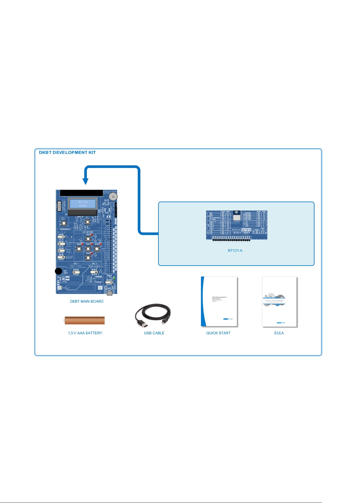
1.1 Package contents
DKBT is delivered with the parts shown in Figure 1 below.
Figure 1: DKBT development kit cont ents
5
Page 5
DKBT overview 2
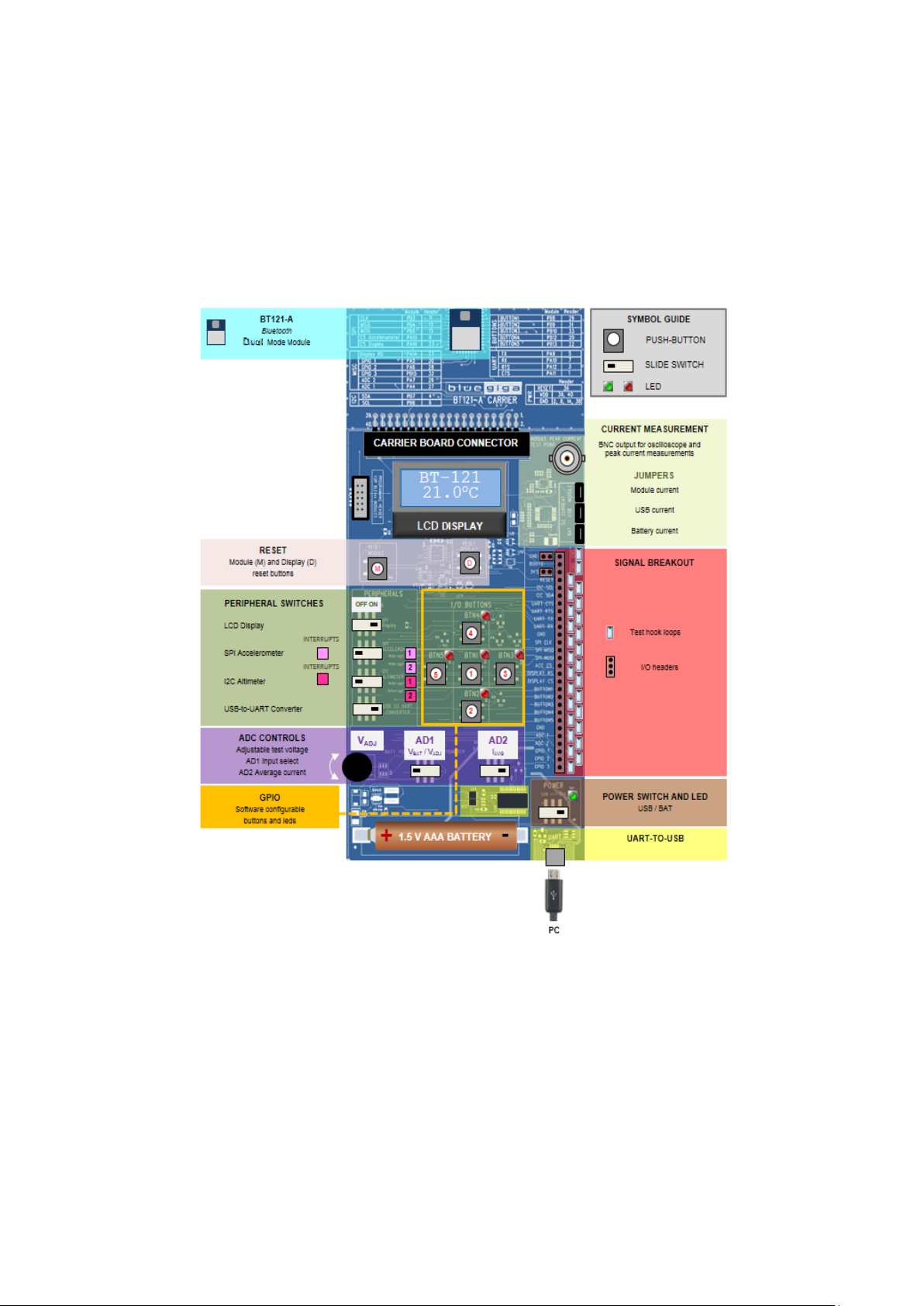
Silicon Labs
This section introduces the functional la yout of the DKBT main board and the BT121 Bluetooth Dual Mode
module carrier board.
An overview of the functional layout of DKBT board and BT121 carrier b oard is shown in Figur e 2 below. The
corresponding functional block diagram is shown in Figure 3 on the following page.
Figure 2: DKBT development kit overview
6
Page 6
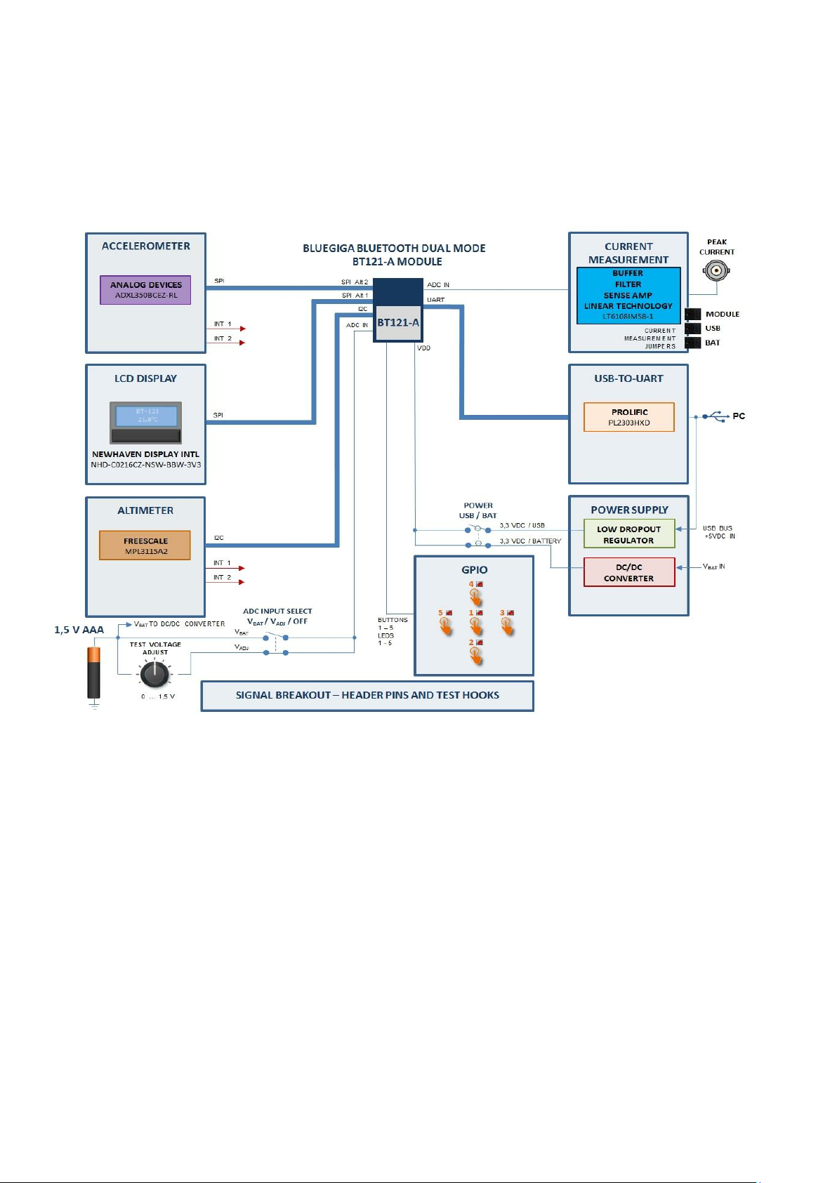
2.1 DKBT functional block diagram
Silicon Labs
The DKBT functional block diagram with essential components and interconnections is shown in Figure 3
below.
Figure 3: DKBT functional block diagram
BT121 Bluetooth Dual Mode module provides vari ous serial interfaces (SPI , I2C, U ART) for connectin g to
peripherals and/or for communicating with other devices such as h ost processors. The SPI bus ( Alt 1 and Alt
2) on the DKBT is connected to an accelerometer and to an LCD display while the I
connected to a precision altimeter/pressure sensor. The accelerometer and altimeter/pressure sensor both
have two interrupt outputs, which are exposed as pads on the DKBT main board.
The DKBT main boar d contains also five push-buttons and five LEDs which c an be controll ed by GPIO of the
BT121. Depending on how the firmware defines the corresponding GPIO pin on the BT121 module, the
switches may be used as inputs. In such cases the correspond ing LED will turn ON when the push-button is
pressed dow n. If the pin has been configured as an output the LE D acts as a visual indicator of the output
state of that part icular GPIO pin. LED’s are b uffer ed by a tr ansistor to pr event loading of the GPIO pins of the
module.
Current measur ement circuitry of f er s the means to measure the peak and a ver a g e current consumption of th e
module or of the whole DK BT board. A BNC c onnector driven by a fast buffer amplifier enables peak current
measurements with the help of an oscilloscope
The UART of the BT121 is connected through a USB-TO-UART converter to a USB c onnec tor which provides
easy connectivity to a PC.
7
2
C bus on the DKBT is
Page 7

Interpreting the silk screens 3
Silicon Labs
DKBT board and the BT121 carrier board have silk scr eens indicating releva nt signals, com ponent s, switches,
buttons etc. The carr ier board silk screen contains signal tables which indicate the nam e of the signal as used
on the DKBT main board, the actua l BT121 module pad name and th e DKBT header connector pin num ber.
An example demonstrating the use of the silk screen information is shown below in
Figure 4.
Note that on the carrier board signal tables Module Pad Name is actually designated as Module
Pin No.
Figure 4: DKBT silk scr een usage example.
8
Page 8

Power supply options 4
Silicon Labs
DKBT development kit can be powered by three methods: by using a 1.5V AAA battery, through a USB
connection or by using an exter nal power supply con nected to the 3V3 / GND h eader pins. Operation of th e
DKBT is identical regardless of the power supply option used.
4.1 Powering with a 1.5V AAA battery
• Install a 1.5 V AAA batt ery into the battery hold er on DKBT noting the correct polarity as m arked on
the battery holder.
• Set the POWER SWITCH to position BAT.
• T
he green POWER LED near the POWER SWITCH should turn on indicating that power is fed t
DKBT. See F igure 5 on next page.
4.2 Powering through USB
• Connect a micro USB cable to the USB connected labeled UART and connect it to a PC or USB
power supply.
• Set the POWER SWITCH to position USB
he green POWER LED near the POWER SWITCH should turn on indicating that power is fed to
• T
DKBT. See F igure 5 on next page.
.
o
4.3 Powering using an external power supply
• Prepare an external power supply by adjusting the output voltage to 3.3 VDC. If the power supply has
adjustable current limit set the current limit to a minimum level of 150 mA to allow normal operation
without current limit.
• Absolute input voltage range is 2.2 - 3.6 VDC or 2.4 - 3.6 VDC when using the internal ADC or DAC of
BT121.
• Attach the positive output of the external power supply to the 3V3 header and the negative output to
the GND header on the DKBT main board.
• POWER SWIT C H may be in either position.
• The green POWER LED near the POWER SWITCH should turn on indicating that power is fed t
KBT. See Figur e 5 on next page.
D
When using the internal ADC or DAC on the BT121 the voltage range is 2.4 - 3.6V.
o
9
Page 9

POWER ON LED
Silicon Labs
USB │BAT
Figure 5: DKBT power supply options
10
Page 10

Measuring the current consumption 5
Silicon Labs
DKBT development kit includes circuitr y, headers and a BNC connect or to ena ble convenient average and
peak current m easurements independent f rom the power supply. You can measure the current consumption
of the whole board or just the current consumed by the Bluetooth module.
Figure 6: Current measurement circuitry and options on DKBT
11
Page 11

One way to measure the current consumption is to use one of the following current measurement headers:
Silicon Labs
AT header can be used to measure DKBT total current consumption when it’s powered with
1. B
battery or external power supply. This test point provides an unfiltered, un-averaged current value
(see NOTE 1 below).
2. USB hea der can b e used to measure the DKBT tota l current c onsumption when it’s powered through
a USB connector. This test point provides an unfiltered, un-averaged current value (see NOTE 1
below).
3. MOD header can be used to measure the BT121 module’s current consumption no matter which
power supply is us ed. This test point provides an unfiltered, un-averaged curr ent value (see NOTE 1
below).
a
Figure 7 Current consumption measurement using MOD, USB and BAT headers
Note 1: The DMM must be in current measurement mode (DC only).
O
ther current measurement options are also included on the DKBT development kit:
• PEAK CURR TEST POINT is a BNC connector for connecting the DKBT BT121 module power supply
line to an oscilloscope for peak current measurements. This test point provides an unfiltered, unaveraged current value converted to voltage (100 mV = 10 mA).
• AVG CURR pro vides the sam e output as th e PEAK CURR TEST PO INT the difference being that the
output is filtered to provide an average current consum ption value. Measurement is m ade with DM
in voltage measurement mode connected to AVG CURR and 0 mA REF header pins. These two
header pins provide a filtered, averaged current value converted to voltage (100 mV = 10 mA).
• 0mA REF provides the zero reference for AVG CURR test point. See description above.
12
M
Page 12

5.1 Measuring average currents with a DMM
Silicon Labs
The current which can be measured through the header conn ections is not filtered or a veraged in any way.
Some current peaks during Bluetooth TX/R X operations are very short and require a high quality DMM to be
used. T o make the aver age current measurem ent easier the DKBT m ain board has built-in c urrent averaging
circuitry m easuring the current flowing i nto the BT121 ’s power suppl y line. The voltage outp uts of this circuitry
are available on the DKBT pin header and are named as 0 mA REF and AVG CURR.
To measure the average current consumption connect a DMM in vo ltage measur ement mode to 0 m A R EF
and AVG CURR header pins. The output is scaled: 100 mV / 10 mA.
Figure 8: Average current measure men t
5.2 Measuring sleep currents with a DMM
Sleep current co nsumption of BT121 is typica lly in the rang e of microamps which means that it important to
use measuring equipment which does not cause excessive errors caused by burden voltage. For most
accurate current measurements with a DMM an external precision current adapter (e.g. μCurrent Gold by
EEVBLOG or s imilar) is needed to remove the effect of burden voltage c aused by the shunt resistor in the
current measurement circuitry (see Figure 9 below). Such adapters may also improve the dynamical
response of the measurement setup drastically.
MOD
Figure 9: Using an external precision current adapter to minimize burden voltage effects in low current measurements.
13
Page 13

5.3 Measuring peak currents with an oscilloscope
Silicon Labs
A typical DMM cannot be used to measure the peak current consumption, since the current peaks are typically
too short to be reliably detected. Also current peaks can be too low to be reliably detected with a DMM.
For measuring th e peak currents there is a BNC con nector on the D KBT main board, which can be used t o
directly connect to a di gital oscilloscope. T he BNC connector output on the DKBT mark ed PEAK CURREN T
TEST POINT (see Figure 10 on next page) provides the m odule current buffered by a Linear Technology
LT6108 (High Side Current Sense Amplifier with Referenc e and Com parator) and is configured to produce an
output of 100 mV / 10 mA.
To measure the peak T X current consumption of the module, c onn ec t a coaxial cable to the BNC connector in
DKBT and to the oscilloscope input. Then run the desired software in the BT121.
Basic recommended settings for the oscilloscope:
• Coupling: DC
• Vertical scale: 200 mV/DIV
• Horizontal scale: 500 µs/DIV
• Level: 400 mV
• Offset: 0.0 V
• Trigger: Normal, rising edge
As stated above, the output on the display corresponds to 100 mV / 10 mA.
Figure 10: Peak current measurement using an oscillos cope.
14
Page 14

Peripherals 6
Peripheral
Interface
Manufacturer / Type
Function
LCD Display
SPI 1 Alt 2
PB14: Display RS
Newhaven Display Intl
Display
Accelerometer
SPI 1 Alt 1
sensor
Analog Devices
Acceleration
Altimeter
I2C 1 Alt 1
PB7: SCA
Freescale
Altitude
Temperature
USB-to-UART
UART
PA12: RTS
Prolific
Bus converter
Button 1
Button 5
PB8
PB13
-
Manual input
LED 1
LED 5
PB8
PB13
-
Visual indicator
Potentiometer
AIN4
PA4
-
ADC test voltage adjust
0 mA reference
AIN6
PA6
-
Current measurement reference
Module average current output
Current sense
AIN7
PA7
-
Current output to ADC
Module average current output
Silicon Labs
DKBT board includes peripherals sensors which can be used in different demo applications or software
prototypes. Ad ditio nal peripherals a nd devices can of c ourse be connect ed to the DKBT via the pin header on
the main board.
Details of the available peripherals including interface pins used with BT121 are listed in T able 1 below.
Converter
Button 2
Button 3
Button 4
LED 2
LED 3
LED 4
PB3: SCK
PB4: MISO
PB5: MOSI
PA14: CS
PA13: CS
PB5: MOSI
PA13: CS ACC
combined with OR-gate (U12 in DKBT)
to form SDA/SDI/SDIO signal for
PB6: SCL
PA9: TX
PA10: RX
PA11: CTS
PB9
PB10
PB12
PB9
PB10
PB12
NHD-C0216CZ-NSW-BBW-3V3
ADXL350BCEZ-RL
MPL3115A2
PL2303HX Rev. D
Pressure
Individual per iphera l switches determ ine only wheth er the SPI (or I2C) bus of the r elated peripheral is
connected or disconnected from the common SPI (or I2C) bus of DKBT. Power suppl y input to the
peripheral is not affected. Switch positions do not have an impact on current consumption.
With all slide-switches OF F BT121 acts completel y in stand-alone mode. All I/O s ignals and busses
are available on the BREAKOUT HEADER connectors and on the TEST HOOK LOOPS.
Table 1: DKBT peripherals
15
Page 15

6.1 Buttons and LEDs
Silicon Labs
There are five push-buttons and five red LED indicators which turn on when the relat ed button is pressed.
These LEDs may also be controlled via the BT121 GPIO pins when the appropriate pins are programm ed to
work as outputs.
6.2 Potentiometer
A trimm er potentiometer can be used to adjust an analog test voltage connected to the i nternal AD-converter
of the BT121 through an electronic relay. Potentiometer can be en abled or disabled with POT/VB AT SENSE
switch.
The POT/VBAT SENSE switch has three positions
OFF = No output to BT121 internal AD input
BAT VOLTAGE = Battery voltage connected to BT121 internal AD input channel AIN4 (PA4)
POT = Potentiometer voltage connected to BT121 internal AD input channel AIN4 (PA4)
6.3 Current sense and 0mA reference
WIth this feature one of the AD input channels (AIN7 / PA7) on the BT121 can be used to measure the
average current consumption of the module itself.
This feature is controlled using the CURRENT SENSE switch, which has two positions:
OFF = No output to BT121 internal AD input
ON = Average current output (100 mV / 10 mA) voltage is connecte d to AD input channel AIN 7 / PA7) on
BT121.
The feature can be enabled/disabled CURRENT SENSE switch.
16
Page 16

6.4 LCD display
Silicon Labs
The LCD display in DKBT is a Newhaven Display International 2 lines x 16 characters backlit display and uses
5 x 8 with cur sor character set. The display has a 4-lin e serial interf ace (SPI bus) which is used f or controlling
the display and for sending characters to be displayed.
The connection schematics between the LCD display and BT121 module are shown below in Figure 11
below.
Figure 11: SPI display connections to BT121 in DKBT
The dual-bit bus transc eive r (74AVC4T245PW ) shown in t he schematics is needed only if physical
isolation is required. If the end-application firmware manages chip selection and alternating
between the use of the interfaces there is no need for the 74 AVC4T245PW t ype of solution. The
purpose of the 74AVC4T 245PW in DKBT is to allow isolating the LCD displa y from t he SPI bus
completely if needed.
The manual RESET button could be replaced by connecting the LCD display RST signal to a
GPIO pin of the BT121. If the power supply used has enough curr ent capability VDD_DISPLAY
could be connected directly to the power supply which feeds the BT121.
17
Page 17

6.5 SPI accelerometer
sensor from the SPI bus
Silicon Labs
The accelerometer in DKBT is the Analog Devices ADXL350BCEZ-RL 3-axis accelerometer with 13-bit
resolution and selectable ranges with m aximum g force at ± 8 g. It also features free fall, tap and double tap
as well activity and inactivity d etection. The d igital output data is f ormatted as 16 -bit t wo’s complement and is
accessible through SPI interface.
The accelerometers interrupt pins are separately available on the DKBT main board.
The connection schematic s between the accelerometer sensor and BT121 module is shown below in Figure
12.
Figure 12: SPI Accelerometer connections to BT121 in DKBT
The Low-Power Dual Buf fer/Line Drivers (74AU P2G126DC) shown in the schematics are need ed
only if the end-application has several SPI bus devices c onnected to BT121. The purpose of the
74AUP2G126DC´s in DKBT is to allow isolating the accelerometer
completely when needed.
The TinyLogic® UHS Two-Input OR Gate NCSZ32 is used to form the SDIO signal for the
accelerometer sensor from BT121 SPI MOSI output and CS ACC signals.
18
Page 18
6.6 I2C altimeter
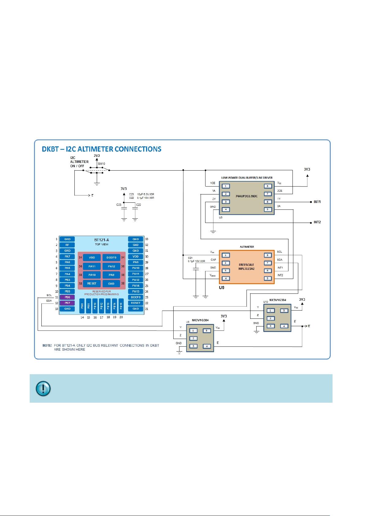
Silicon Labs
The altim eter in DKBT is t he Freescale MPL3115A2 which prov ides very accur ate pressure and altitude data.
It has digital output, two interrupts for auto-wake, minimum/maximum threshold detection and autonomous
data acquisition.
The altimeters interrupt pins are separately available on the DKBT main board.
The connectio n schematics between the accelerometer chip and BT121 modul e is shown below in F igure 13.
Connection to BT121 is very simple and r equ ires only the use of two NXP analog switches (Low-ohmic singlepole single-throw analog switch NX3V1G384GW) to isolate the SCL and SDA signal lines when required.
Figure 13: I2C Altimeter connections to BT121 in DKBT
The two NXP analog s witches shown in the schematics needed if the end-application has m ore
than one SPI device conne cted to the same SPI interface on the BT121 an d if the firmware does
not manage chip selection to prevent bus contention issues.
19
Page 19

Related documentation 7
Silicon Labs
The following documents contain relevant and/or useful inform ation and is recommended reading for anyone
developing applications for the BT121 module.
T121 Data Sheet
• B
More details about the BT121 Bluetoo th Dual Mode module hardware can be found from the data
sheet.
•
DKBT Development Kit design materials
DKBT deve lopment kit design mater ials ( schematics, PCB drawing, BoM) are av ailable for downloa
and can be used as a reference design.
•
B
The Blu etooth Dual Mode s oftware getting started gu ide explains the ar chitecture of the Bluetooth
stack software, the available APIs and devel opm ent options and also contains a brief int roduct ion to
the PC tools and the software development flow.
luetooth Dual Mode Software Getting Started Guide
d
20
Page 20

Simplicity Studio
One-click access to MCU and wireless
tools, documentation, software, source
code libraries & more. Available for
Windows, Mac and Linux!
IoT Portfolio
www.silabs.com/IoT
Disclaimer
Silicon Labs intends to provide customers with the latest, accurate, and in-depth documentation of all peripherals and modules available for system and software implementers using or
intending to use the Silicon Labs products. Characterization data, available modules and peripherals, memory sizes and memory addresses refer to each specific device, and “Typical”
parameters provided can and do vary in different applications. Application examples described herein are for illustrative purposes only. Silicon Labs reserves the right to make changes
without further notice to the product information, specifications, and descriptions herein, and does not give warranties as to the accuracy or completeness of the included information.
Without prior notification, Silicon Labs may update product firmware during the manufacturing process for security or reliability reasons. Such changes will not alter the specifications or
the performance of the product. Silicon Labs shall have no liability for the consequences of use of the information supplied in this document. This document does not imply or expressly
grant any license to design or fabricate any integrated circuits. The products are not designed or authorized to be used within any FDA Class III devices, applications for which FDA
premarket approval is required, or Life Support Systems without the specific written consent of Silicon Labs. A “Life Support System” is any product or system intended to support or
sustain life and/or health, which, if it fails, can be reasonably expected to result in significant personal injury or death. Silicon Labs products are not designed or authorized for military
applications. Silicon Labs products shall under no circumstances be used in weapons of mass destruction including (but not limited to) nuclear, biological or chemical weapons, or
missiles capable of delivering such weapons. Silicon Labs disclaims all express and implied warranties and shall not be responsible or liable for any injuries or damages related to use of
a Silicon Labs product in such unauthorized applications.
Trademark Information
Silicon Laboratories Inc.®, Silicon Laboratories®, Silicon Labs®, SiLabs® and the Silicon Labs logo®, Bluegiga®, Bluegiga Logo®, ClockBuilder®, CMEMS®, DSPLL®, EFM®,
EFM32®, EFR, Ember®, Energy Micro, Energy Micro logo and combinations thereof, “the world’s most energy friendly microcontrollers”, Ember®, EZLink®, EZRadio®, EZRadioPRO®,
Gecko®, Gecko OS, Gecko OS Studio, ISOmodem®, Precision32®, ProSLIC®, Simplicity Studio®, SiPHY®, Telegesis, the Telegesis Logo®, USBXpress®, Zentri, the Zentri logo and
Zentri DMS, Z-Wave®, and others are trademarks or registered trademarks of Silicon Labs. ARM, CORTEX, Cortex-M3 and THUMB are trademarks or registered trademarks of ARM
Holdings. Keil is a registered trademark of ARM Limited. Wi-Fi is a registered trademark of the Wi-Fi Alliance. All other products or brand names mentioned herein are trademarks of
their respective holders.
Silicon Laboratories Inc.
400 West Cesar Chavez
Austin, TX 78701
USA
http: //www.silabs.com
SW/HW
ww.silabs.com/simplicity
w
Quality
ww.silabs.com/quality
w
Support & Community
abs.com/community
www.sil
 Loading...