

Page 1

BT121 BLUETOOTH DUAL MODE MODULE
DATA SHEET
Wednesday, 3 March 2021
Document Version: 1.63
Page 2

Silicon Labs
VERSION HISTORY
Date Edited
Comment
1.0
First release of document
1.1
Minor updates
1.2
Minor updates
1.3
Power consumption measurements
1.4
Revised power consumption measurements
1.41
FCC, IC, Japan and Korea certification info updated
1.42
Various corrections and edits, corrected front page +10dBm LE power
number and RF specification +9dBm both to the +7dBm setting used in the
module for regulatory compliance
1.43
Wake-up pin section added
1.44
Mass production part numbers added to ordering code list.
1.45
Typo corrections related to the note concerning I2C 2.
I2C 2 can be used only in Alt 2 configuration.
1.46
Certificates section under FCC separation between human body and antenna
changed from 9 mm to 7 mm.
SWD bus clarification : PA13 = SWDIO and PA14 = SWCLK
1.47
Altered outline and footprint drawings to render properly in PDF
1.48
Sleep mode current updated
1.49
Reset description elaborated, fixed I2C schematic, added number of
piconets, wake-up sources corrected
1.50
Fixed SPI slave select descriptions
1.51
SDK and SDA pins in Figure 21 corrected to SCL and SDA with correct
placement
1.52
Minor changes
1.53
Contact information updated
1.6
Added dimension details for the 8 center pads for programming and testing
Editorial and layout fixes
Page 3

Silicon Labs
1.61
Corrected the maximum number of simultaneous connections
Corrected Bluetooth version compliance
1.62
Renamed "Smart Ready" to "Dual Mode" and "Classic" to "BR/EDR"
according to the official Bluetooth SIG nomenclature.
1.63
Updated certification information
Page 4

Silicon Labs 4
TABLE OF CONTENTS
BT121 overview 6
1.1 Key Features 6
1.2 Typical applications 7
1.3 Block diagram 7
Design guidelines 8
2.1 PCB layout recommendations 8
2.2 Power supply recommendations 8
2.3 Software application related options 8
2.4 Firmware updating related recommendations 8
Pin-out description 10
3.1 Power, ground, reset, RF and boot loader pins 10
3.2 GPIO pins 11
Power control 12
4.1 Power supply requirements 12
4.2 Power saving functionality 12
4.3 Reset 13
4.4 Recovery mode 14
4.5 Clock signals 14
Interfaces 15
5.1 GPIO 15
5.2 UART 16
5.3 I2C 16
5.4 SPI 16
5.5 ADC 16
5.6 DAC 16
5.7 Real-time clock 16
5.8 Microcontroller programming interface 16
Antenna 17
6.1 Effect on antenna matching of a plastic sheet placed near the antenna 17
6.2 Effect on antenna matching of a metal sheet placed under the antenna 19
6.3 Effect on antenna matching of a metal sheet placed against the end of the module 20
6.4 Measured antenna efficiency 21
6.5 Measured 2D radiation patterns 22
6.6 Measured 3D radiation patterns 24
Bluetooth Stack Software 25
Host interface 26
Page 5

Silicon Labs 5
8.1 UART 26
Connection examples 27
9.1 Connecting an external host using the UART interface 27
9.2 Connecting an external device using SPI interface 28
9.3 Connecting an external device using I2C interface 29
Electrical characteristics 30
10.1 Absolute maximum ratings 30
10.2 Recommended operating conditions 30
10.3 Logic signal characteristics 31
10.4 Power consumption 33
RF Characteristics 35
11.1 Supported frequencies and channels 35
11.2 Typical receiver sensitivity 35
11.3 Transmitter output power 35
11.4 Carrier frequency accuracy 35
Physical dimensions 36
Soldering recommendations 38
13.1 Soldering profile example 39
Tape and reel packaging 40
14.1 Reel material and dimensions 40
14.2 Tape material and dimensions 40
14.3 Tape and reel box dimensions 41
14.4 Module orientation in tape 41
Certifications 42
15.1 Bluetooth 42
15.2 CE 42
15.3 FCC 42
15.4 IC 43
15.5 MIC Japan 45
15.6 KC (South-Korea) 45
Ordering information 46
Contact Information 47
Page 6

Silicon Labs 6
BT121 overview
BT121 is a Bluetooth Dual Mode module targeted for applications that require both Bluetooth LEand BR/EDR
connectivity. It can connect to legacy devices that only support Bluetooth SPP or Apple® iAP2 profiles as well
to devices that support Bluetooth LE. BT121 integrates a high performance Bluetooth radio, a low-power ARM
Cortex micro-controller and a Bluegiga Bluetooth Dual Mode stack software marking it extremely easy-to-use
as no RF or Bluetooth software development is needed. BT121 can be used as a modem together with a
separate host MCU, but applications can also be embedded into the built-in ARM® Cortex® MCU with the
Bluegiga BGScriptTM scripting language.
1.1 Key Features
Bluetooth features
• Bluetooth 4.1 Dual Mode compliant
• Master and slave modes
• Up to 6 x BR/EDR connections
• Up to 7 x BLE connections
• 1 x BR/EDR + 6 x BLE connections
simultaneously
• Scatternet: 3 simultaneous piconets, 1 as
master + 2 as slaves
Radio features
• Integrated antenna
• TX Power
o +12 dBm with Bluetooth BR/EDR
o +8 dBm with Bluetooth LE
• RX Sensitivity
o -96 dBm
• 200-400 meter LoS range
Software features
• Integrated Bluetooth Dual Mode Stack
• SPP, iAP2, HID and GATT over BR Bluetooth
profiles
• Any GATT based Bluetooth LE profile
• 1000 kbps throughput over SPP
• BGAPITM serial protocol API over UART for
network co-processor usage
• BGLIBTM host C library which implements
BGAPI serial protocol
• BGScriptTM scripting language for standalone
usage
• Profile ToolkitTM for creating GATT based
services
Hardware interfaces
• UART host interface
• 2 x SPI, UART and 2 x I2C peripheral interfaces
• Up to 22 x GPIO with interrupts
• 4 x 12-bit ADC
• Internal battery voltage measurement option
Microcontroller
• ARM Cortex M0
• 48 MHz
• 16kB RAM
• 128kB flash
Electrical characteristics
• Supply voltage: 2.2V to 3.6V
• Supply voltage: 2.4V to 3.6V when using ADC
Environmental and regulatory
• Temperature range: -40C to +85C
• Bluetooth, CE, FCC and IC, Japan and South-Korea
qualified
Dimensions:
• 11.0 mm x 13.9 mm x 2.2 mm (W x L x H)
Page 7
Silicon Labs 7
1.2 Typical applications
BT121 can be used in a wide variety of applications such as cable replacement, HID devices, health and fitness,
PoS (point-of-sales), M2M connectivity, automotive aftermarket, industrial and home automation gateways and
others.
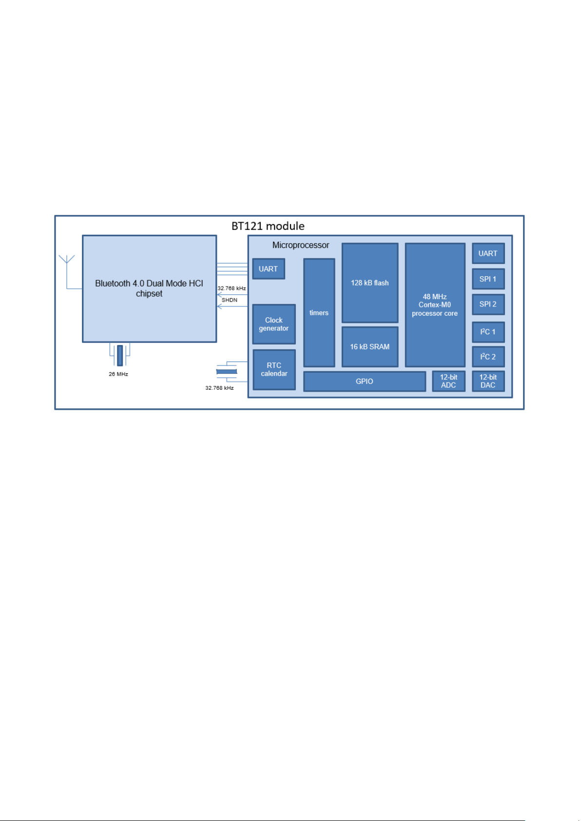
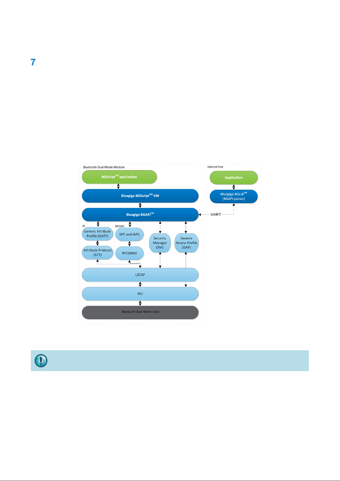
1.3 Block diagram
The block diagram for Bluegiga Bluetooth Dual Mode module BT121 is shown in below.
Figure 1 BT121 Bluetooth Dual Mode module block diagram
Page 8
Silicon Labs 8
Design guidelines
Certain hardware related design guidelines should always be followed when developing applications based on
the BT121 module.
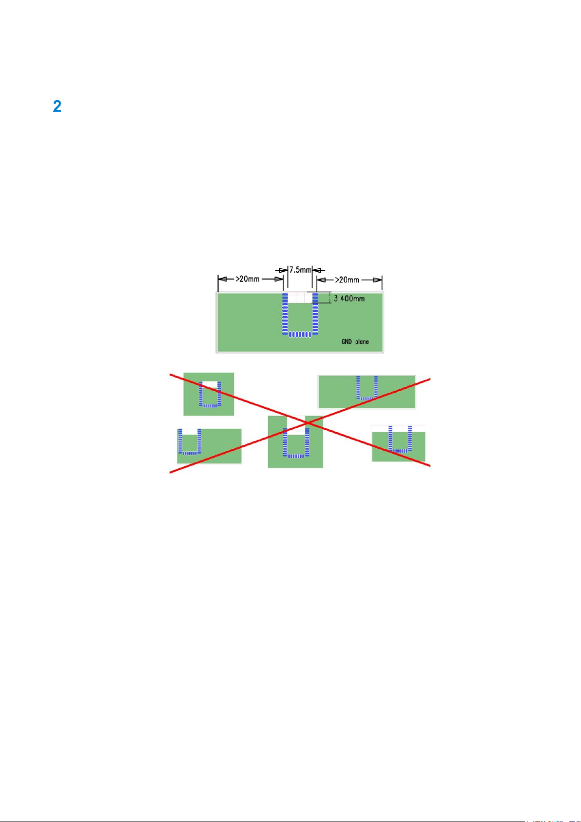
2.1 PCB layout recommendations
• All ground pads should be connected to a ground plane.
• The antenna layout should follow the example shown in Figure 2 below and avoid the designs shown
as crossed over.
• BT121 requires minimal free space around the module and only the white area marked in the PCB
picture series presented in Figure 2 below needs to be free of copper and components.
Figure 2 PCB layout recommendations for BT121 application boards
2.2 Power supply recommendations
The regulator used must be capable of supplying a peak current of 150 mA and the regulator must be of a type
stable with ceramic capacitors.
2.3 Software application related options
BT121 can be used either as a stand-alone solution by using the Bluegiga BGScript™ scripting language or
alternatively if the application software size or other factors require together with an external host processor by
using Bluegiga BGAPI™ commands. The decision on which approach to use is most often dictated by the limits
set by the internal memory of the BT121 module.
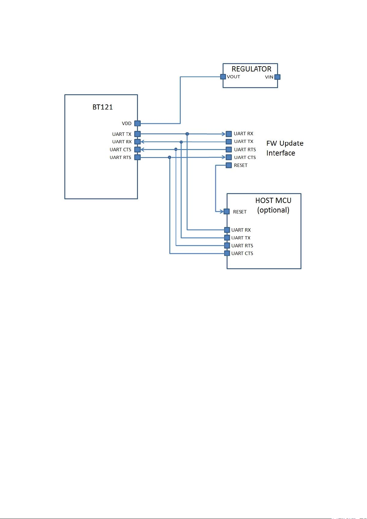
2.4 Firmware updating related recommendations
To enable firmware updating an external UART interface connection as shown in Figure 3 on the next page is
mandatory. BT121 firmware can be updated through the UART interface by holding the host MCU in reset state
which typically will free the UART lines to be used by the update interface.
Page 9
Silicon Labs 9
Figure 3 BT121 firmware update via UART connection example
Page 10
Silicon Labs 10
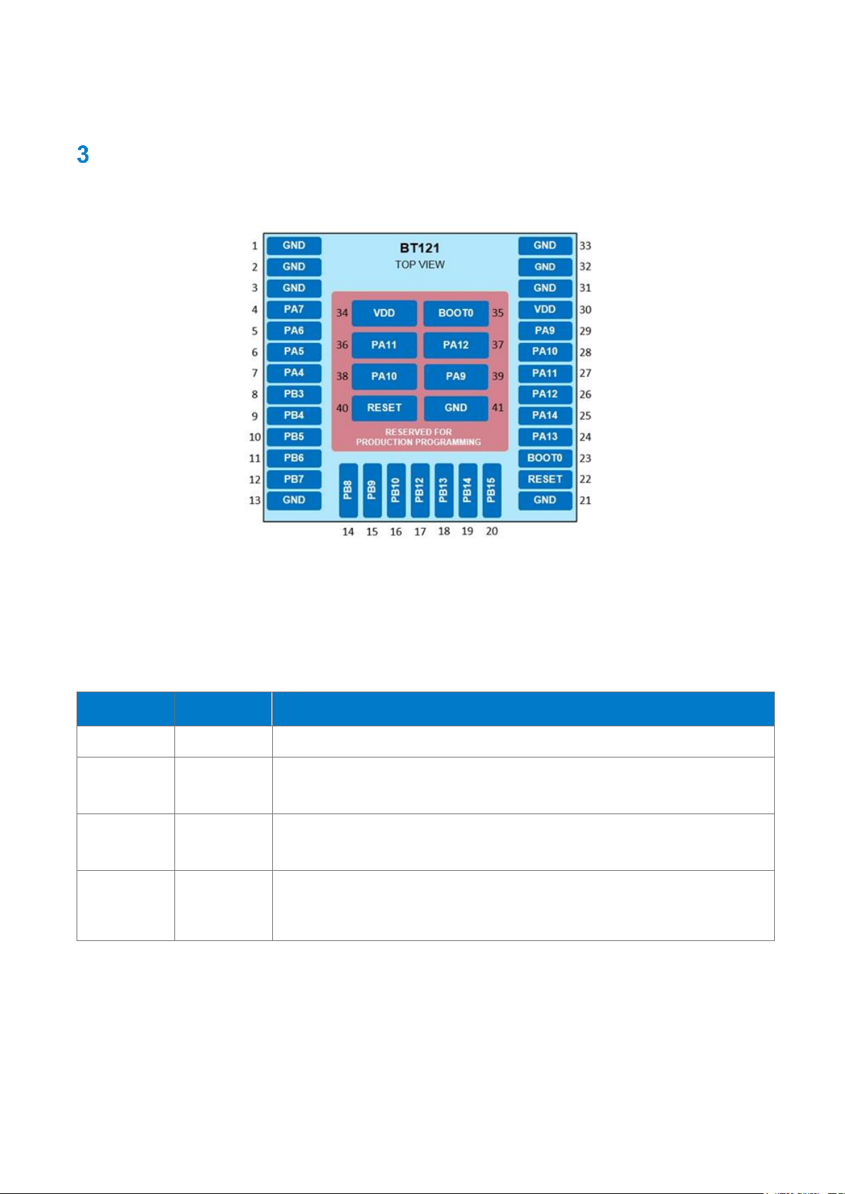
Pin-out description
This section contains a description of the BT121 pin-out. Each pin may have one or more functions which are
all listed in tables. The pin-out is shown in Figure 4 below.
Figure 4 BT121 pin-out (top view)
3.1 Power, ground, reset, RF and boot loader pins
Power supply, ground, reset signal, RF antenna input/output and boot loader related pins are listed in Table 1
below.
Pin / Pad
Function
Description
30,34
VDD
Module power supply input pins.
1, 2, 3, 13, 21,
31, 32, 33, 41
GND
Ground pin. These are all connected together internally but they should all be individually
connected directly to a solid ground plane with vias in close proximity to the pins. This requirement
concerns especially the antenna connections.
22,40
RESET
Module reset signal pins. Pulling RESET low will reset the internal processor of the module. These
connections have an internal pull-up and can be left floating if not needed. The RESET pin s forced
low internally on power-on. External reset sources should be open drain.
23,35
BOOT0
Boot mode pin of the microcontroller internal boot loader. This connection has an internal pulldown and should be left floating or pulled low in normal operation.
If the Bluegiga DFU is overwritten or disabled, pulling BOOT0 high at reset will allow DFU to be
rewritten through the UART (serial port interface).
Table 1 Power, ground, reset, RF and boot loader pins
Page 11

Silicon Labs 11
3.2 GPIO pins
General purpose I/O pins and their functions are listed below.
PERIPHERAL
FUNCTION
GPIO NAME
PA7
PA6
PA5
PA4
PB3
PB4
PB5
PB6
PB7
PB8
PB9
PB10
PB12
PB13
PB14
PB15
PA13
PA14
RTS
PA12
CTS
PA11
RX
PA10
TX
PA9
PIN NUMBER
4 5 6 7 8 9 10
11
12
14
15
16
17
18
19
20
24
25
26
37
27
36
28
38
29
39
DEFAULT
FUNCTION **
dc
dc
dc
dc
dc
dc
dc
dc
dc
dc
dc
dc
dc
dc
dc
dc
dc
dc
RTS
CTS
RX
TX
5V TOLERANT
N N N N Y Y Y Y Y Y Y Y Y Y Y Y Y Y Y Y Y Y UART ***
RTS
CTS
RX
TX
SPI 1
Alt.1
MOSI
MISO
SCK Alt.2
SCK
MISO
MOSI
SPI 2
Alt.1 SCK
MISO
MOSI
Alt.2 SCK
MISO
MOSI
I2C 1
Alt.1 SCL
SDA Alt.2 SCL
SDA
I2C 2
Alt.1
Alt.2 SCL
SDA
DAC output
AO2
AO1
ADC input
AIN7
AIN6
AIN5
AIN4
Interrupt
channel
7 6 5 4 3 4 5 6 7 8 9
10
12
13
14
15
13
14
12
11
10
9
Table 2 General purpose I/O pins and their functions
GPIO pins 36, 37, 38 and 39
** Default pin functions on production firmware / dc = disconnected, no need to pull up or down Reserved for production testing
*** UART can be used as a BGAPI™ host interface and DFU firmware updates Must be left unconnected
If the pins are set as GPIO rather than UART signals the DFU cannot work, see UART (Section 5.2 ) and recovery mode (Section 4.4 )
I2C 2 can be used only Alt. 2 configuration
Page 12

Silicon Labs 12
Power control
4.1 Power supply requirements
BT121 is powered by a single power supply input (VDD). Nominal input voltage is 3.3 VDC and input voltage
range 2.2 V to 3.6 V. If the module’s internal ADC and/or DAC functions are used minimum allowed power
supply voltage is 2.4V.
The VDD supply should be capable of supplying a peak current of at least 150 mA even though the average
current consumption of BT121 will be much less than that. External high frequency bypass capacitors are not
needed because the module contains the necessary power supply filtering capacitors.
Careful design of the layout and proper component selection are necessary to prevent switching noise from
appearing on the supply line. Such disturbances can be caused by on-board charge pump converters (e.g.
RS232 level shifters). Charge pump based converters tend to have strong switching spikes which are difficult
to filter out and may degrade RF performance. A ferrite chip can be added in series with the supply line close
to the module supply pin to reduce RF interference through the supply line.
There is a total of about 1.5 µF of ceramic capacitors on the VDD line inside the module. When using low drop
linear regulators to generate a regulated supply voltage for the VDD line, the stability of the regulator with the
low ESR provided by these capacitors should be checked. Many linear regulators and some switched mode
ones too are not stable when used with ceramic output capacitors. The regulator datasheets usually have
recommendations for output capacitor ESR range or they contain a stability curve to help select components
properly. A regulator designated as “stable with ceramic capacitors” is recommended.
4.2 Power saving functionality
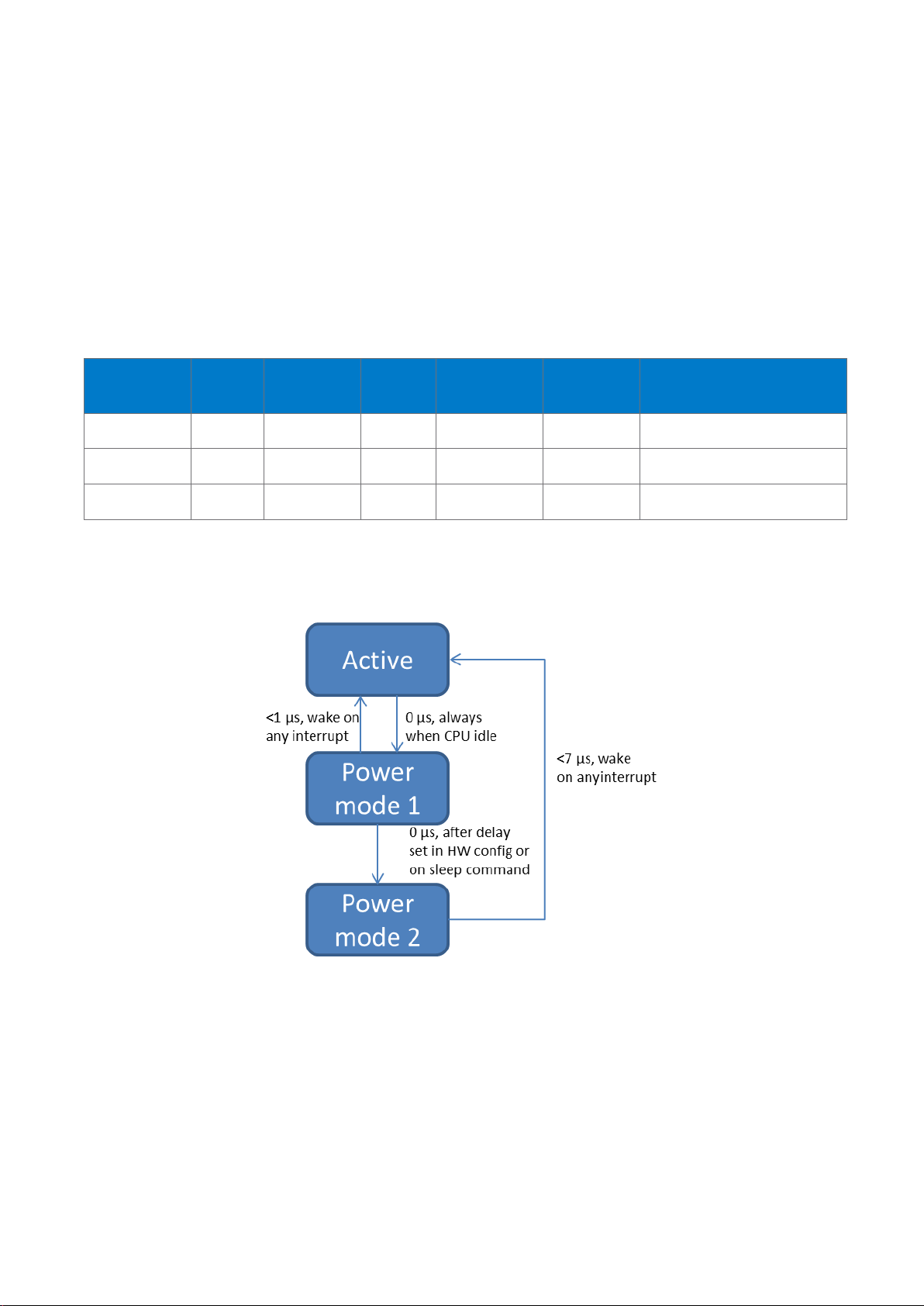
BT121 contains two configurable power saving modes. The internal RTC (Real Time Clock) is usually kept
always running to avoid the long wake-up time associated with the internal 32 kHz crystal oscillator. The RTC
is always available to wake up the module.
4.2.1 Power mode 1
Power mode 1 is a shallow sleep state with all clocks and peripherals running but with the processor core
stopped. It is used automatically and has no impact on module performance and does not require special
considerations in user applications. See Table 3 on next page.
4.2.2 Power mode 2
Power mode 2 is a deep sleep state, in which most peripheral devices and system clocks are powered down.
The UART interfaces cannot operate without clocks, and instant communications with the host are not possible.
A separate wake-up pin can be used to wake up the module, which will stay on as long as the wakeup pin is
held high. GPIO interrupts, activity on the radio and RTC interrupts can also cause a wake-up event. There is a
short wake-up delay due to the time required for the internal clocks to stabilize and because of this the module
processor is not instantly ready to receive data. See Table 3 on next page.
4.2.3 Wake-up pin functionality
This feature can be used to prevent to Bluetooth module from entering a sleep mode or alternatively can be
used to wake it up from a sleep mode. If the sleep modes have been enabled in the hardware configuration file
(see Bluetooth Dual Mode Configuration Guide) and use UART to communicate with the module, then this
feature must be enabled and the wake-up pin must be asserted before sending any data or BGAPI commands
to the module, and also kept asserted until the last byte has been transferred into the module over the UART.
Page 13
Silicon Labs 13
The wake-up pin functionality can only be assigned to a single GPIO, but it is still possible to assign normal
GPIO interrupts to other pins. The difference between the wake-up pin and normal GPIO interrupts is that the
wake-up pin will not only generate the interrupt which wakes the module, but will also keep the module awake
as long as it is held in the asserted state. Normal GPIO interrupts can wake the module from any state but after
the interrupt event handler completes the module will return to sleep.
There is always a delay before the module wakes up. It is possible to measure the wake-up time by measuring
when flow control starts to work. Data should not be sent before the module has waken up to prevent data loss.
Monitor the RTS/CTS signal to detect when the module has waken up. There is no special command separately
to wake up the module.
Power
mode
CPU
clocks
CPU
core
Radio
Wakeup
delay
UART
Current
consumption *
Active
ON
Running
On - Active
10 - 20 mA
Power mode 1
ON
Sleep
On
< 1μs
Active
4 - 10 mA
Power mode 2
OFF
Stopped
On
< 7 μs
Off
50 - 100 μA
Table 3 Power modes with corresponding wakeup delays and current consumption
* Current consumption with radio inactive
The logic flow of the power saving modes in relation to each other is shown in Figure 5 below. It is to be noted
that the processor will not lose RAM contents regardless of the power mode used.
Figure 5 Power modes in relation to each other and to active mode
4.3 Reset
BT121 can be reset by several methods: by pulling the RESET pin low, by the internal system power-up reset
functionality or by the internal watchdog timer. The RESET pin is internally connected to a pull-up resistor with
a resistance of approximately 40 kohm. The RESET pin should be connected to a push-button, header or test
point to enable the use of the system recovery mode.
Page 14

Silicon Labs 14
On an internal reset, the RESET pin will be briefly pulled low internally. It is recommended that an external reset
source is of an open drain type.
4.4 Recovery mode
Pulling the BOOT0 pin high at reset sets the BT121 module’s internal microcontroller into a recovery mode,
which allows the Bluegiga DFU to be rewritten to the module using the BGTOOL software. The BOOT0 pin
should be connected to a header or test point to enable DFU recovery. The pin is internally connected to a 10
kohm pull-down resistor.
4.5 Clock signals
BT121 generates all the required clock signals internally. The clocks used by the internal microcontroller and
external peripherals are synchronized to an internal 32.768 kHz crystal connected to the internal RTC. The
micro power RTC is always kept running when the module is supplied with power. It will take approximately two
seconds for the RTC oscillator to stabilize after power is connected. To avoid this delay it is recommended that
the power supply feed to the BT121 is not switched off but instead the module can be set into the lowest power
mode providing the smallest current consumption.
Page 15
Silicon Labs 15
Interfaces
5.1 GPIO
BT121 contains a number of pins which can be configured to operate as general purpose digital I/O’s, analog
inputs or outputs or to be used in combination with various built-in functions. The module contains I2C, SPI,
UART, touch pad sensing and various timer functions. Most of the pins are 5V tolerant. All GPIO pins can drive
currents of up to +/- 8 mA (up to 20mA with relaxed voltage specifications).
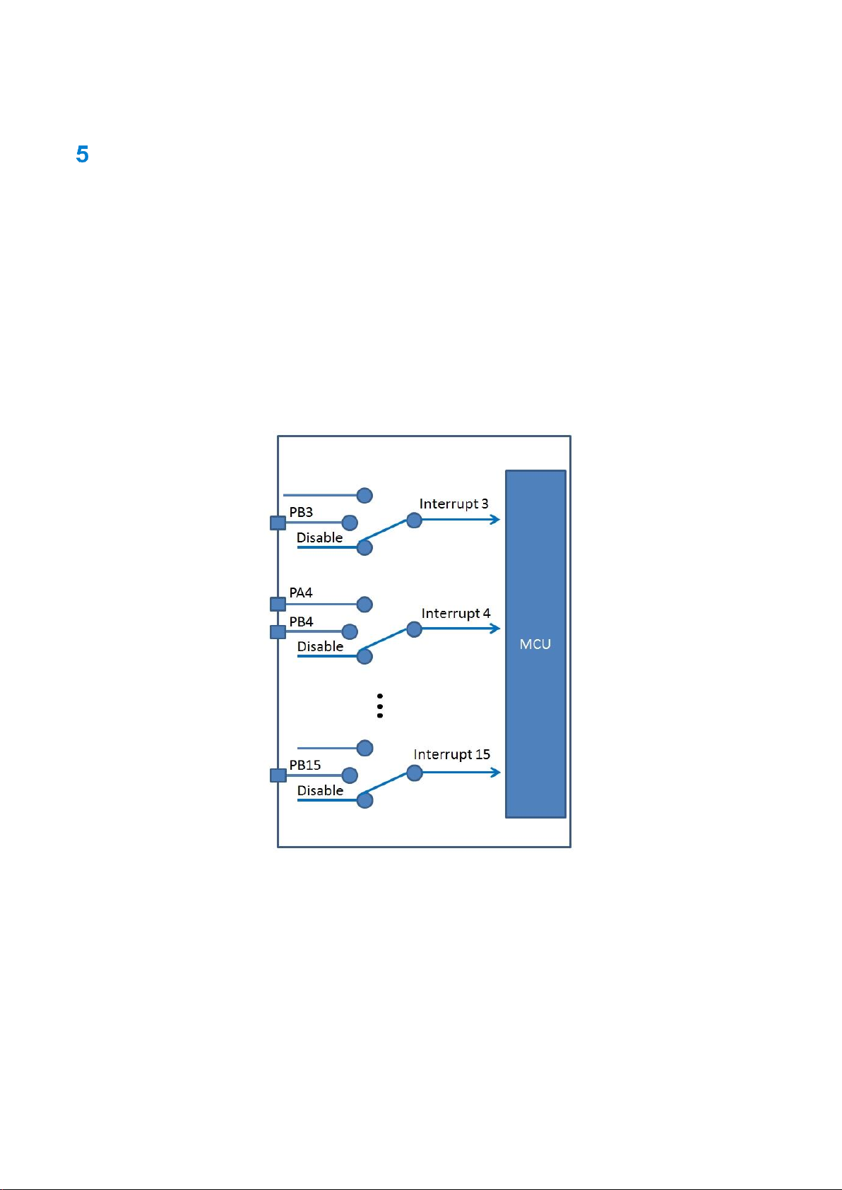
5.1.1 GPIO interrupts
Any GPIO signal can be assigned an interrupt function. However, the module microcontroller has a limited
number of interrupt channels available for GPIO’s. The microcontroller has two separate GPIO ports, with the
external signals divided between the two. An interrupt can be assigned to a specific port signal number from
either port, but not for the same number on both ports simultaneously. The principle of GPIO interrupt
multiplexing on the Bluegiga Bluetooth Dual Mode module BT121 is shown in Figure 6 below.
Figure 6 GPIO interrupt multiplexing scheme
Page 16

Silicon Labs 16
5.2 UART
There is one UART port available on the BT121. By default, it is used for BGAPI™ host interface but with
BGScript™ it can be used as an application UART. The UART supports all standard baud rates up to 4 Mbps.
RTS/CTS handshake scheme is supported and recommended for every application for reliable data transfer.
5.3 I2C
BT121 has up to two I2C ports available. Both support standard mode up to 100 kbps, fast modes up to 400
kbps and Fast Mode Plus with improved drive capability and clock stretching up to 1 Mbps.
5.4 SPI
BT121 has up to two SPI ports available. Both can be configured for frame sizes from 4 to 16 bits and clock
frequencies up to 18 MHz. Both ports provide internal CRC calculation. Software-controlled GPIO’s should be
used as slave select signals.
5.5 ADC
BT121 contains a 4-channel 12-bit ADC with multiple external input sources as well as an internal battery
measurement and temperature measurement possibility. ADC input voltage range is 0 to VDD.
5.5.1 Accessory functions of the ADC
In addition to the external ADC inputs an internal temperature sensor or internal supply voltage divider can be
selected as the input to ADC.
Power supply range when using internal ADC functions is 2.4 to 3.6 VDC.
5.6 DAC
BT121 contains a 2-channel 12-bit DAC, with two independent outputs. DAC output voltage range is 0 to VDD.
Power supply range when using internal DAC functions is 2.4 to 3.6 VDC.
5.7 Real-time clock
BT121 contains a real-time clock (RTC) with full calendar support and sub-second resolution. The RTC can be
used for periodic or specifically programmed wakeups. The RTC is clocked by an internal crystal oscillator which
is always on as long as power is supplied to the module.
5.8 Microcontroller programming interface
The preferred method of programming the BT121 is by using the Bluegiga DFU through the UART host interface.
A problem may occur if the DFU is disabled by disabling the UART or if the DFU is overwritten accidentally.
Then the DFU would need to be re-uploaded.
The two methods of DFU uploading are through the SWD interface (PA13 = SWDIO and PA14 = SWCKLK)
using an ARM serial debug adapter, or by forcing the BOOT0 signal high and by resetting the module to make
it boot into a recovery mode. Then the BGTool software can be used to recover the DFU through the UART
interface.
Page 17
Silicon Labs 17
Antenna
The internal chip antenna on the BT121 uses the application board ground plane as part of the antenna, and
requires at least 20 mm of ground plane on both sides of the module to radiate with optimal efficiency. BT121
must be placed on the application board edge, preferably roughly in the middle of the board edge. The ground
plane can be internal to the application PCB, allowing components to be placed on both sides of the module
and on both sides of the application board. The module ground pads in the antenna end should be connected
to the main ground plane layer with vias in immediate proximity of the pins. Thermal reliefs on the ground pins
have a negligible effect on antenna performance. Typical antenna matching curves are shown in Figure 7
below.
Figure 7 Typical antenna matching
The antenna used on the BT121 is quite robust with regard to adverse effects of close-by metallic materials.
The PCB thickness will not affect the antenna operation significantly. The application board can be installed with
the PCB bottom side and the antenna edge directly against a plastic casing without adverse effects. On the
module top side, there should be at least 3 mm of clearance to the nearest object.
The antenna requires a 7.5 x 3.4 mm sized copper clearance in all layers, with no components or traces on the
opposite side of the PCB from the antenna. Sufficient metal clearance is mandatory because the antenna will
not function at all without a sufficient opening in the ground plane.
Any metal in close proximity of the antenna will prevent the antenna from radiating freely. It is recommended
not to place any metal or other conductive objects closer than 10 mm to the antenna except in the directions of
the application board ground planes.
A board cutout is not required for the antenna. In fact, a cutout would cause the antenna to be detuned which
in turn will degrade range significantly. The module is also not to be placed in a cut-out recess on the board
edge or in the middle of the board which has a central cutout.
On the following pages are examples on how plastic or metal sheets in several different orientations and
distances to the antenna effect antenna matching.
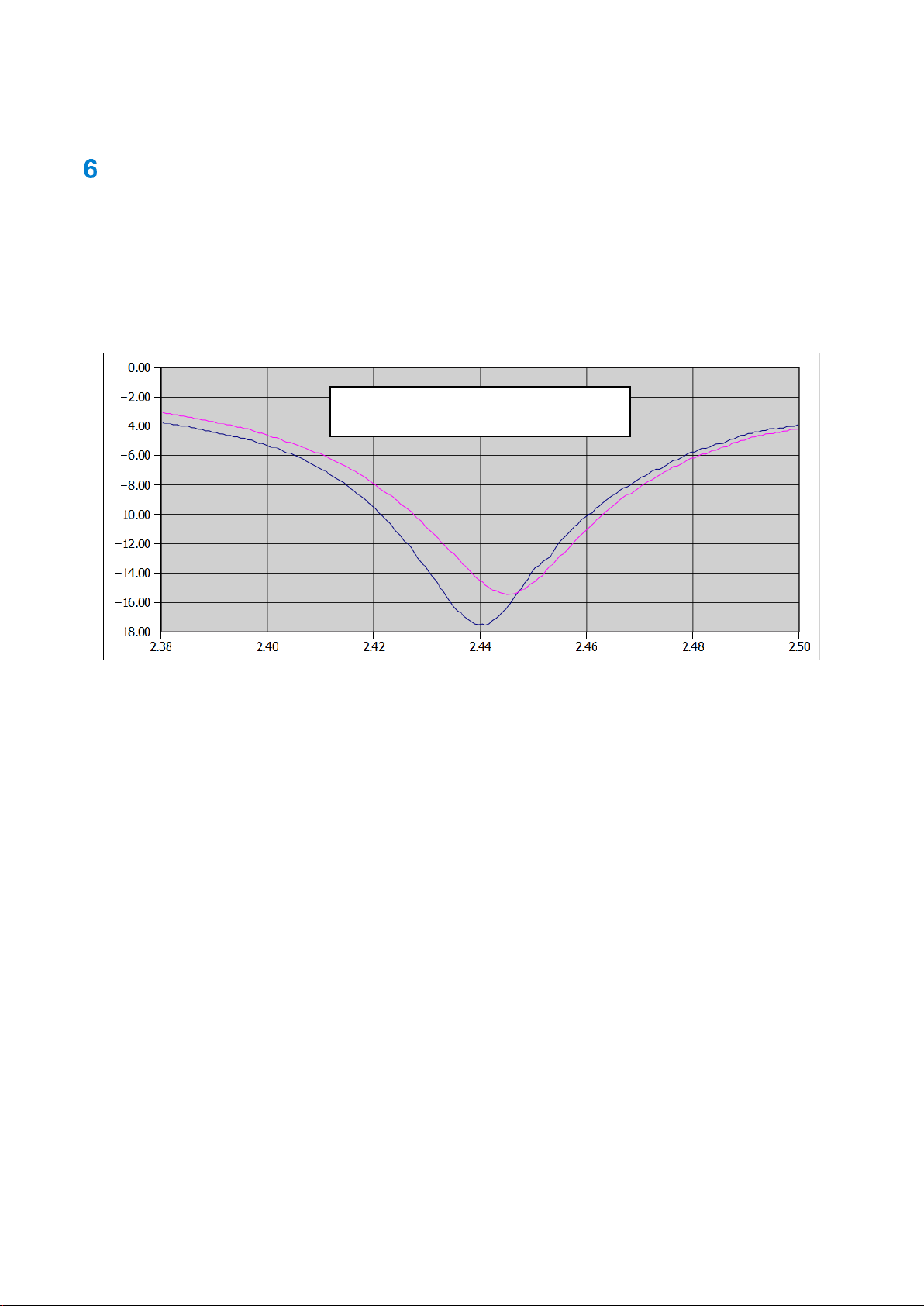
6.1 Effect on antenna matching of a plastic sheet placed near the antenna
As an example on how a plastic sheet placed in the vicinity of the module and/or antenna effect the antenna
matching we can examine Figure 8 below.
Violet curve: with thermal reliefs
Blue curve: without thermal reliefs
Page 18
Silicon Labs 18
Figure 8 Proximity effect of a 3 mm plastic sheet on antenna matching with different placements
Blue curve
Plastic sheet under antenna touching PCB
Violet curve
Plastic sheet against antenna at module end
Yellow curve
Plastic sheets under antenna touching PCB
and against antenna at module end
Page 19
Silicon Labs 19
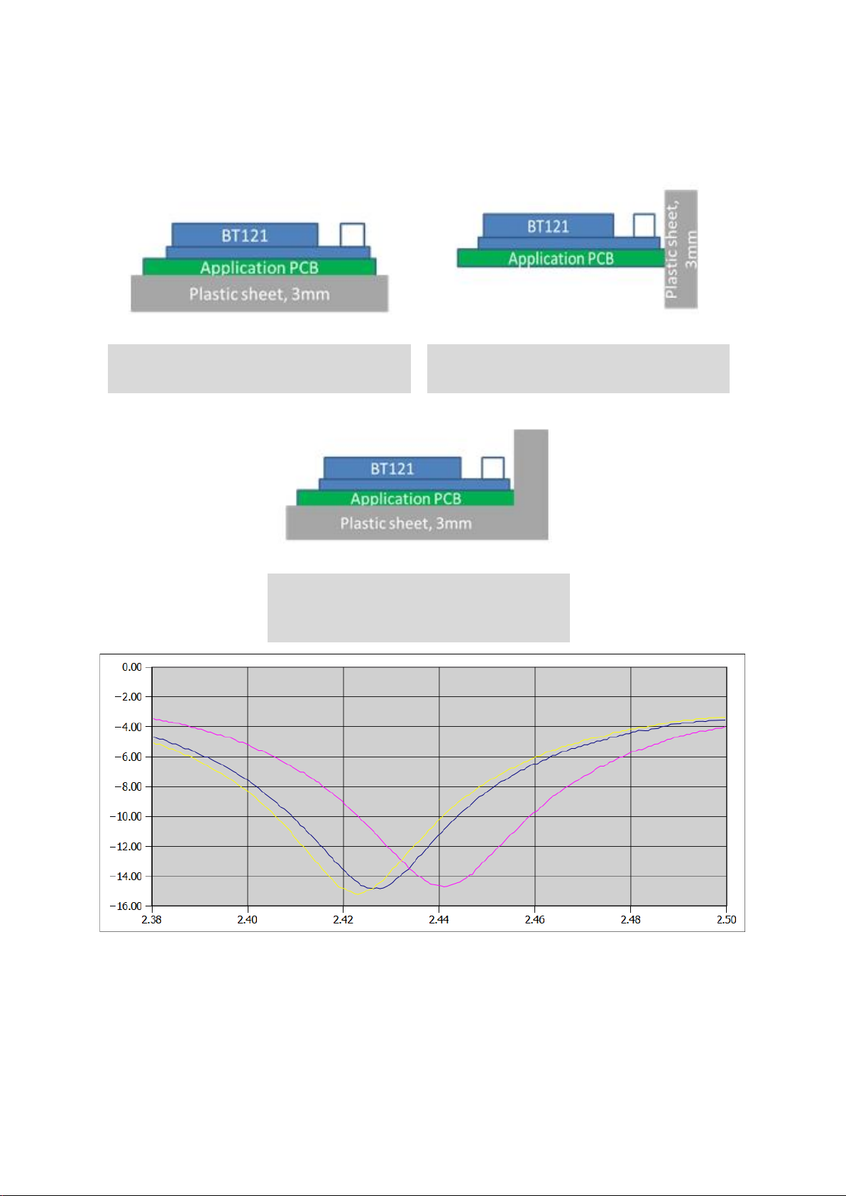
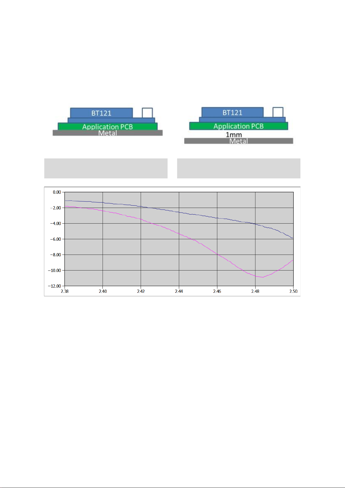
6.2 Effect on antenna matching of a metal sheet placed under the antenna
As an example on how a metal sheet placed in the vicinity of the module and/or antenna effect the antenna
matching we can examine Figure 9 below.
Figure 9 Effect of a metal sheet placed under the antenna on antenna matching
Violet curve
Metal sheet under antenna touching PCB
Blue curve
Same as on the left but distance is 1 mm
Page 20

Silicon Labs 20
6.3 Effect on antenna matching of a metal sheet placed against the end of the
module
As an example on how a metal sheet placed in the vicinity of the module and/or antenna effect the antenna
matching we can examine Figure 10 below.
Figure 10 Effect of a metal sheet placed under the antenna on antenna matching
Violet curve
Metal sheet against end of module end
Violet curve
Metal sheet at module end 5 mm distance
Page 21
Silicon Labs 21
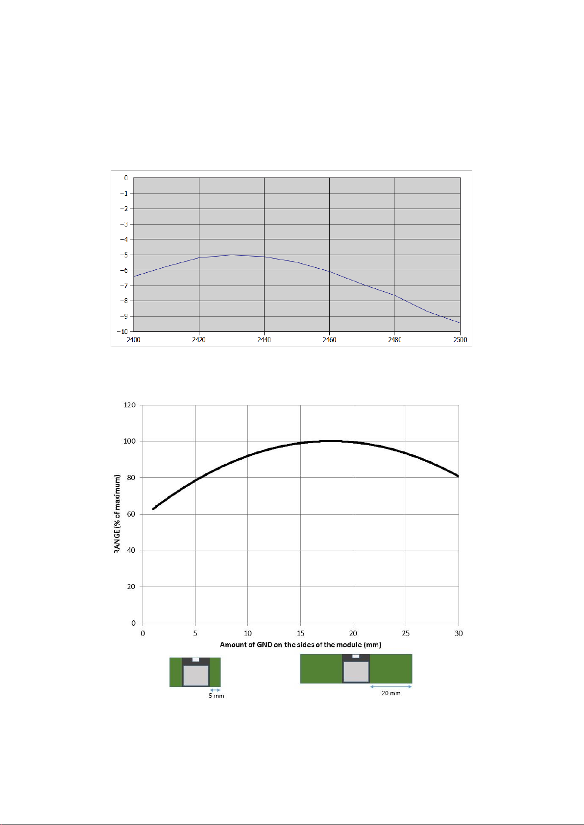
6.4 Measured antenna efficiency
The measured antenna efficiency as a function of frequency is shown in Figure 11 below.
Figure 11 Antenna efficiency related to frequency
Figure 12 Impact of the size of GND plane to the range of BT121
Page 22
Silicon Labs 22
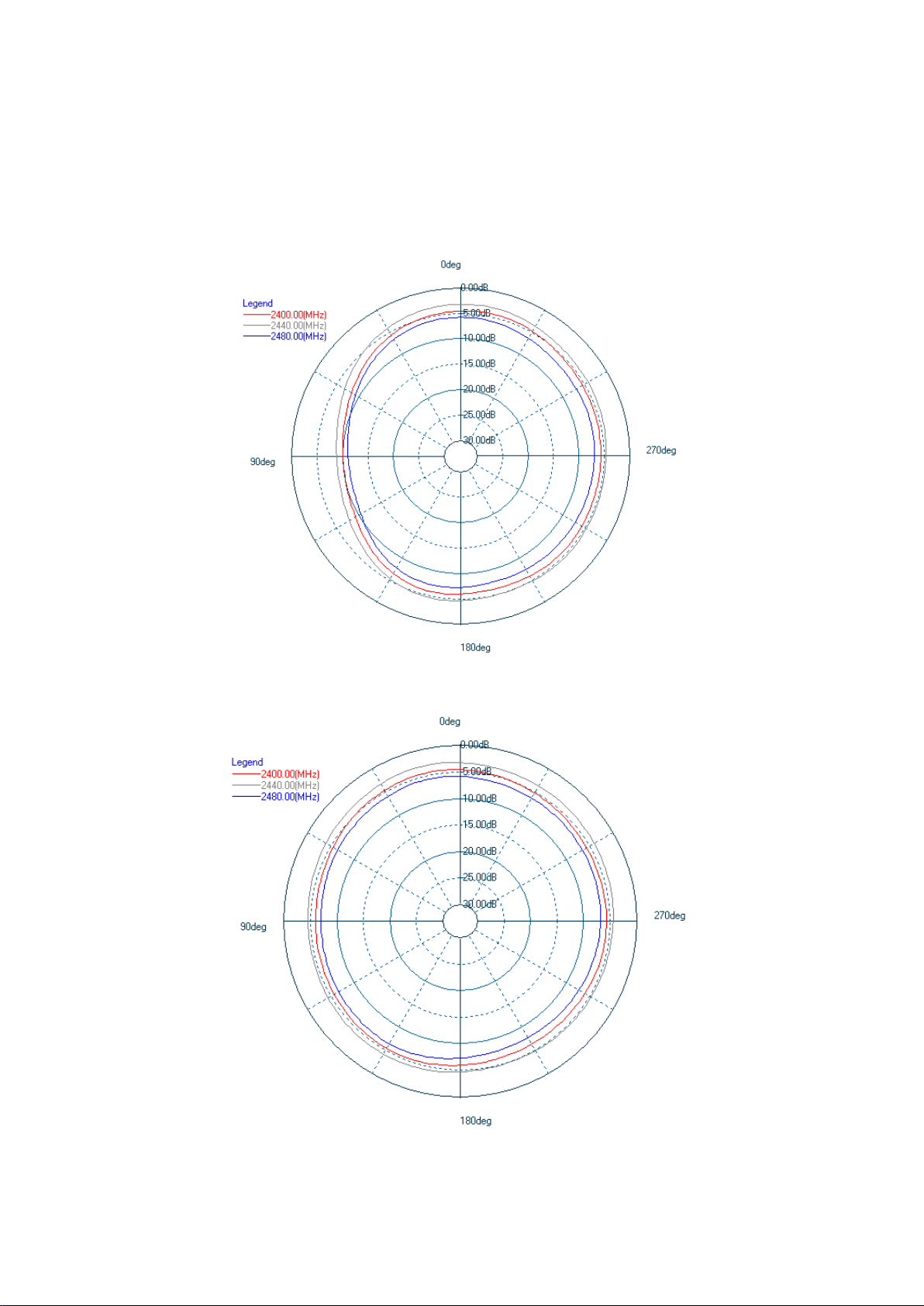
6.5 Measured 2D radiation patterns
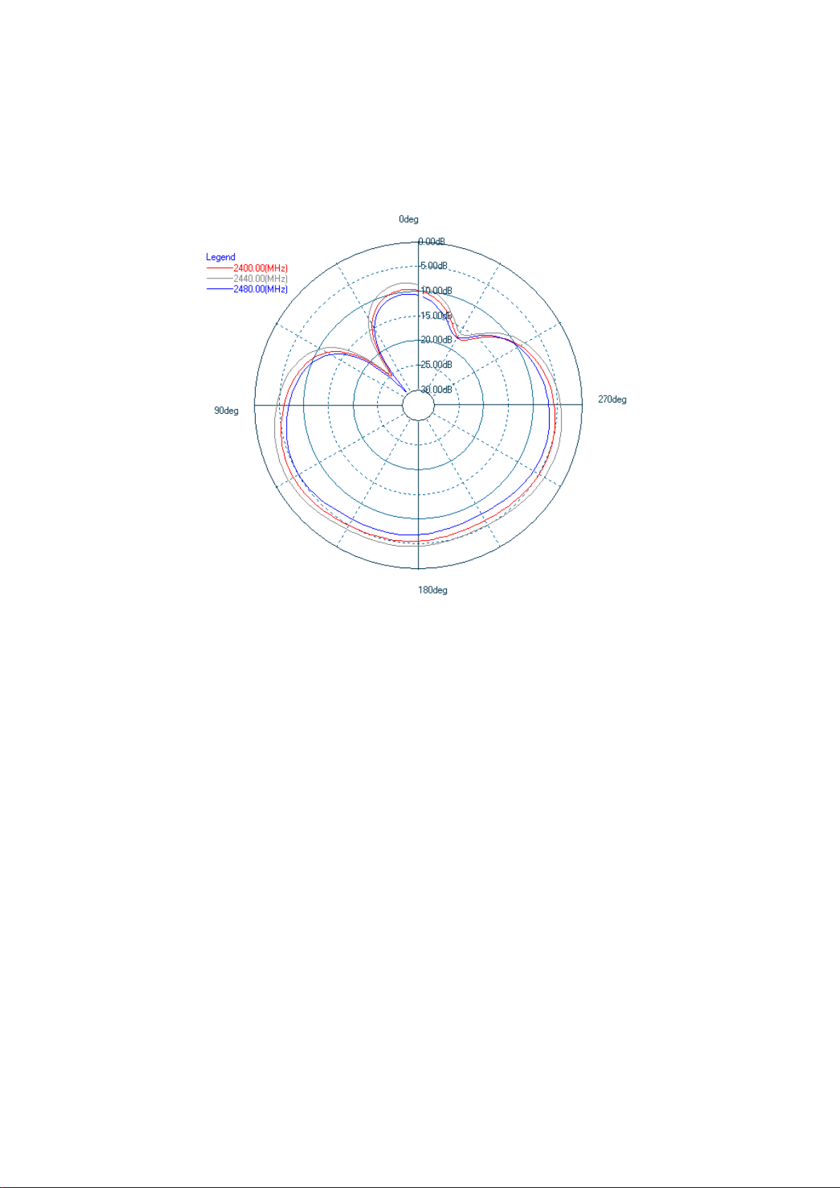
Typical radiation patters of the BT121 module on the DKBT carrier board as 2D plots are shown below in Figure
13 (view from module side), Figure 14 (view from antenna end) and on the following page in Figure 15 (view
from above module).
Figure 13 Typical 2D radiation pattern for BT121 with view from module side
Figure 14 Typical 2D radiation pattern for BT121 with view from antenna end side
Page 23
Silicon Labs 23
Figure 15 Typical 2D radiation pattern for BT121 with view from above module
Page 24

Silicon Labs 24
6.6 Measured 3D radiation patterns
Typical radiation patters of the BT121 module on the DKBT carrier board as 3D plots are shown below. Figure
16 represents a radiation pattern from module end side opposite to antenna and Figure 17 from above the
module.
Figure 16 Typical 3D radiation pattern for BT121 with view from module end opposite to antenna
Figure 17 Typical 3D radiation pattern for BT121 with view from above the module
Page 25
Silicon Labs 25
Bluetooth Stack Software
Bluegiga's Bluetooth Dual Mode Software is a complete Bluetooth Dual Mode software stack for BT121
Bluetooth Dual Mode module. The software implements a full Bluetooth BR/EDR and LE compatible Bluetooth
Stack and L2CAP, RFCOMM, SMP and ATT protocols as well as Bluetooth SPP, HID, Apple iAP2, GATT over
BT profiles and any GATT based Bluetooth LE profile.
The Bluetooth Dual Mode Software also is supported by a complete SDK for developing Bluetooth Dual Mode
applications using either an external host or BGAPITM serial protocol over UART or fully standalone applications
based on a simple scripting language called BGScriptTM.
Several profiles and software project examples are offered as part of the Bluetooth Dual Mode SDK to help
expedite the development of Bluetooth Dual Mode compatible end-user products.
The main parts of the Bluegiga Bluetooth Dual Mode software stack are shown below.
Figure 18 Bluegiga Bluetooth Dual Mode software stack
To learn more about the Bluetooth Dual Mode software stack, the SDK and the APIs please read
Bluetooth Dual Mode Software Getting Started Guide.
Page 26

Silicon Labs 26
Host interface
8.1 UART
For applications where an external host such as MCU is used BT121 can be controlled over the UART interface
using the BGAPI
TM
serial protocol.
For reliable communications can data transfer the hardware flow control RTS/CTS signals must be used in the
UART interface.
It is also recommended that the accuracy of the clock of the controlling host should be 1% or better for the
UART signaling to work reliably with speeds exceeding 115200 kbps (maximum baud rate is 4 Mbps).
Default UART settings are listed below:
Parameter
Default setting
UART baud rate
115200
RTS/CTS flow
control
Enabled
Data bits
8
Parity
None
Stop bits
1
Table 4 BT121 UART interface default settings
Page 27

Silicon Labs 27
Connection examples
The following sections show how to connect a Bluegiga Bluetooth Dual Mode module with various external
devices using the UART, SPI and I2C interface.
9.1 Connecting an external host using the UART interface
The connection to an external host is done using the UART interface of the module. This interface is also used
for module reprogramming using the DFU method and thus an optional connector should be provided on the
application PCB to allow reprogramming if needed. A typical solution then is to hold the host in reset state which
will keep the UART pins of the host floating, allowing the interface to be used for programming the module by
using e.g. a PC and suitable software. See Figure 19 .
40
GND
GND
GND
PA7
PA6
PA5
PA4
PB3
PB4
PB5
PB6
PB7
GND
PA11
GND
GND
GND
VDD
PA9
PA10
PA12
PA14
PA13
BOOT0
RESET
GND
VDD
PA10
RESET
BOOT0
PA12
PA9
GND
PB8
PB9
PB10
PB12
PB13
PB14
1
2
3
4
5
6
7
8
9
10
11
12
13
14 15 16 17
18 19
PB15
20
RX
RTS
33
32
31
30
29
28
26
25
24
23
22
21
34
36
38
41
35
37
39
BT121
RESERVED FOR
PRODUCTION PROGRAMMING
TX
TOP VIEW
27
PA11
CTS
BT121
UART
3V3
EXTERNAL HOST
MICROPROCESSOR
3V3
RX
TX
RTS
CTS
VDD
VSS
HOST
UART
GND NC RX TX RTS CTS RST VDD
RESET
3V3
OPTIONAL CONNECTOR ON APPLICATION PCB
ALLOWS CONTROL AND REFLASH OF MODULE
FOR EXAMPLE FROM A PC
Figure 19 Connecting an external host with BT121 using UART
Page 28

Silicon Labs 28
9.2 Connecting an external device using SPI interface
Bluegiga Bluetooth Dual Mode module BT121 contains two physical SPI peripherals (SPI 1 and SPI2) each with
alternative configurations (Alt 1 and Alt 2). All of the four optional configurations can be used to connect different
types of peripheral devices to the module. Pin configurations for the four SPI interface options are listed in Table
2. An example of this type of interfacing is shown in Figure 20 below. In the example below a generic EEPROM
memory peripheral chip is connected to the BT121 using the SPI 1 Alt 2 option.
Figure 20 Connecting an external device with BT121 using SPI interface
Page 29
Silicon Labs 29
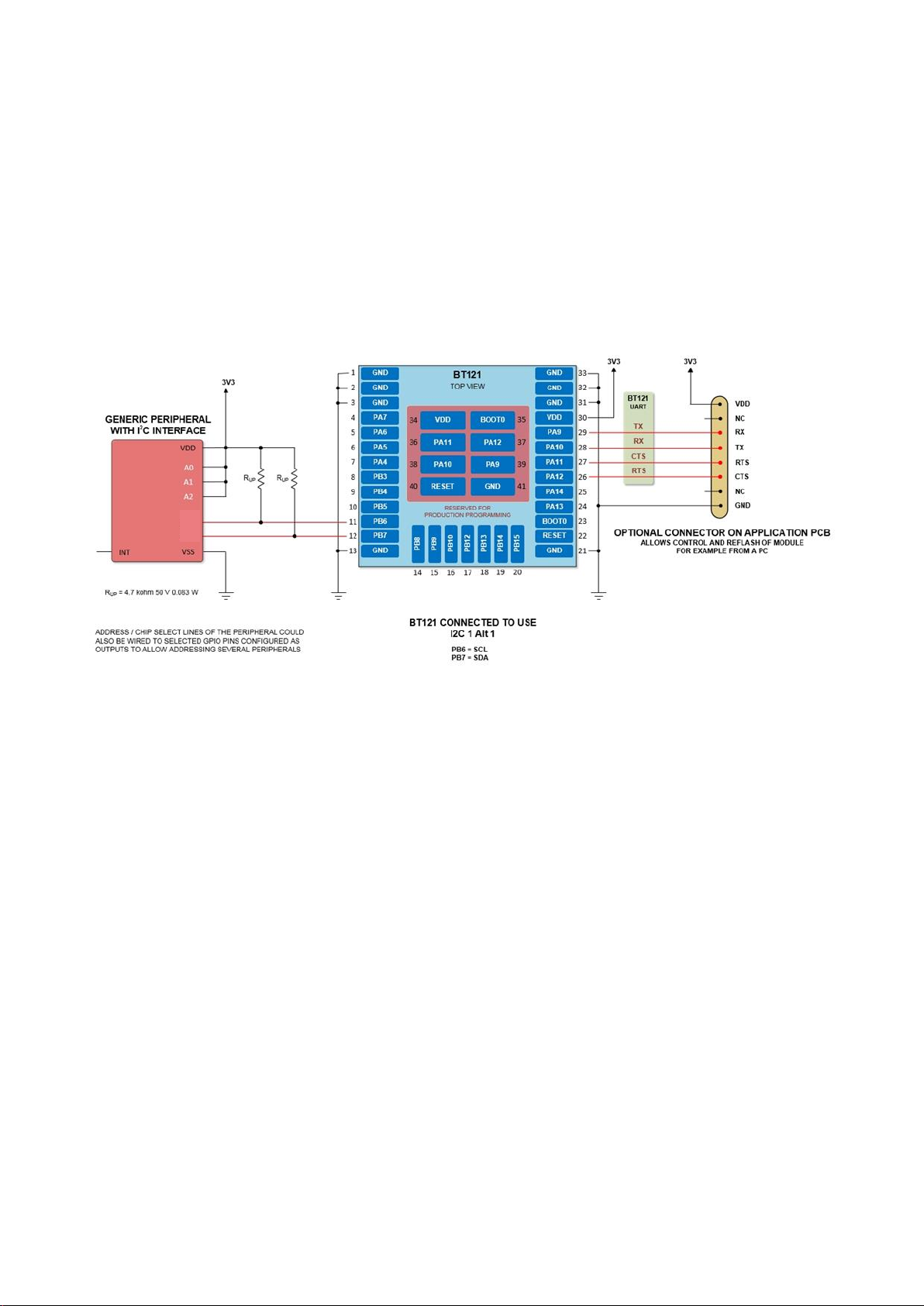
9.3 Connecting an external device using I2C interface
Bluegiga Bluetooth Dual Mode module BT121 contains two physical I2C peripherals (I2C 1 and I2C 2). I2C 1 has
two alternatives (Alt 1 and Alt 2) and I2C 2 one alternative (Alt 2). All of the three optional configurations can be
used to connect different types of peripheral devices with the module. Pin configurations for the three I2C
interface options are listed in Table 2. An example of this type of interfacing is shown in Figure 21 below. Note
the pull-up resistors on the SDA and SCL lines. The example shows the address/chip select lines of the generic
peripherals hardwired to VDD but in practice all or some of them would be wired to GPIO pins of the BT121
configured to work as chip select or address lines controlled by the application hardware. In the example below
a generic sensor chip is connected to the BT121 using the I2C 1 Alt 1 option.
Figure 21 Connecting to an I2C peripheral
SCL
SDA
Page 30

Silicon Labs 30
Electrical characteristics
10.1 Absolute maximum ratings
Parameter
Min
Max
Unit
Storage temperature
-40
85
°C
VDD
-0.3
3.6
V
5V tolerant GPIO voltages
-0.3
5.5
V
Other terminal voltages
-0.3
VDD+0.3
V
Output current sourced or sunk by any GPIO pad
25
mA
Current on all GPIO pads combined
120
mA
Table 5 Absolute maximum ratings
10.2 Recommended operating conditions
Rating
Min
Max
Unit
Operating temperature range
-40
85
°C
VDD
2.2
3.6
V
VDD (when operating ADC or DAC)
2.4
3.6
V
Table 6 Recommend operating conditions
Page 31

Silicon Labs 31
10.3 Logic signal characteristics
10.3.1 Digital I/O
Digital I/O pins
Min
Typ
Max
Unit
Input voltage levels
VIL input logic level low 1.7V ≤ VDD ≤ 3.6V
-0.3
-
0.3VDD
V
VIH input logic level high 1.7V ≤ VDD ≤ 3.6V
0.7 VDD
-
VDD + 0.3
V
Output voltage levels
VOL output logic level low, Vdd = 3.6 V, Iol = 7 mA
- - 0.4
V
VOH output logic level high Vdd = 3.6 V, Ioh = -12 mA
VDD - 0.4
-
VDD
V
Table 7 Digital I/O pin electrical characteristics
10.3.2 Reset
Power-on Reset
Min
Typ
Max
Unit
Power on reset threshold (rising edge)
1.84
1.92
2.00
V
Power on reset threshold (falling edge)
1.80
1.88
1.96
V
RESET signal pulse width (pulled low)
1.5 - -
ms
Table 8 Reset pin characteristics
10.3.3 ADC
Power-on Reset
Min
Typ
Max
Unit
ADC input impedance
- - 50
kohm
ADC input voltage range
0 - VDD
V
ADC differential nonlinearity error
-
0.7
1.3
LSB
ADC integral nonlinearity error
-
0.8
1.7
LSB
ADC offset error
- 1 2.8
LSB
ADC gain error
-
0.5
3
LSB
Table 9 ADC pin characteristics
Page 32

Silicon Labs 32
10.3.4 DAC
Power-on Reset
Min
Typ
Max
Unit
DAC output load impedance
5 - -
kohm
DAC output voltage range
0.2
-
VDD - 0.2
V
DAC differential nonlinearity
- - 2
LSB
DAC integral nonlinearity
- - 4
LSB
DAC offset error
- - 12
LSB
DAC gain error
- - 0.5
%
Table 10 DAC pin characteristics
Page 33

Silicon Labs 33
10.4 Power consumption
Operation state
Current
Unit
Description
CPU active
14
mA
CPU active
RF idle
Power state 1 - RF idle
6.7
mA
CPU idle
RF idle
Power state 2 - RF idle
81
µA
CPU sleep
RF idle
Reset state
6-13
mA
Reset-signal held low
Continuous transmission -
BDR
92
mA
+12dBm, CPU active
Continuous transmission -
EDR
85
mA
+12dBm, CPU active
Table 11 Typical power consumption of different operating states
Operation state
Current
Unit
Description
Idle, not visible, not connectable
6.0
mA
Idle, visible, connectable
6.7
mA
Inquiry
38.7
mA
Connected, no data
11.1
mA
Connected, no data, sniff 1s
6.6
mA
Connected, continuous data
15.8
mA
115.2kbps over BGAPI
Connected, continuous data, 1s
sniff
7.2
mA
115.2kbps over BGAPI
Table 12 Typical power consumption, BR/EDR Bluetooth (Master mode, CPU sleep disabled)
Operation state
Current
Unit
Description
Idle, visible, connectable
800
µA
Inquiry
33
mA
Connected, no data
5.1
mA
Page 34

Silicon Labs 34
Connected, no data, sniff 1s
520
µA
Connected, continuous data
15.8
mA
115kbps over BGAPI*
Connected, continuous data,
sniff 1s
7.2
mA
115kbps over BGAPI*
Table 13 Typical power consumption, BR/EDR Bluetooth (Master mode, CPU sleep enabled)
*sleep controlled by wakeup pin, in the constant UART data streaming test the CPU is not allowed to enter sleep
mode
Operation state
Current
Unit
Description
Advertising, not connectable
1.4
mA
108ms
Advertising, connectable
1.7
mA
108ms
Advertising, not connectable
242
µA
1000ms
Advertising, connectable
280
µA
1000ms
Table 14 Typical power consumption, Bluetooth Low Energy (CPU sleep enabled)
Page 35

Silicon Labs 35
RF Characteristics
11.1 Supported frequencies and channels
Parameter
Min
Max
Unit
Frequency
2402
2480
MHz
Channels 0 78
CH #
Table 15 Supported frequencies and channels
11.2 Typical receiver sensitivity
Packet type
-40 to 85oC
Unit
DH1
-95
dBm
2DH1
-96
dBm
3DH3
-88
dBm
LE
-96
dBm
Table 16 Typical receiver sensitivity
11.3 Transmitter output power
Modulation type
Min
Typ
Max
Unit
BDR (1 Mbps)
10
12
14
dBm
EDR (2, 3 Mbps)
7 9 11
dBm
LE
5.5
7
8.5
dBm
Table 17 Transmitter output power at maximum setting
11.4 Carrier frequency accuracy
Parameter
Typ
Max
Bluetooth limit
(total error)
Unit
Variation between individual units
3
10
+/- 25
ppm
Variation with temperature (-40 to
+85oC)
9
15
+/- 25
ppm
Table 18 Carrier frequency accuracy
Page 36

Silicon Labs 36
Physical dimensions
Figure 22 BT121 module physical dimensions
Figure 23 BT121 module recommended PCB pad pattern
Page 37

Silicon Labs 37
The 8 center pins of the module are reserved for production programming and testing and should
be left unsoldered but despite of this unmasked traces and vias should NOT be placed under the
module in order to prevent short circuits.
Figure 24 BT121 module side view dimensions
Page 38

Silicon Labs 38
Soldering recommendations
Bluegiga Bluetooth Dual Mode module BT121 is compatible with the industrial standard reflow profile for Pbfree solders. The reflow profile to be used depends on the thermal mass of the entire populated application
PCB, heat transfer efficiency of the oven and on the particular type of solder paste used. Consult the datasheet
of the particular solder paste used for more detailed information regarding profile configurations.
The following recommendations for soldering the module are to ensure reliable solder joints and operation of
the module after soldering. Since the soldering profile used is process and layout dependent, the optimum
profile should be studied and decided case by case.
The following recommendation should be taken only as a starting point and should be adjusted according to
more detailed instructions of the solder paste and soldering equipment manufacturers.
• Check the recommended soldering profile configuration from the solder paste manufacturers
documentation.
• Avoid using more than one flow.
• Reliability of the solder joints and self-alignment of the component are dependent on the solder volume.
A minimum stencil thickness of 150 m is recommended.
• Aperture size of the stencil should be 1:1 with the pad size.
• A low residue, “no clean” solder paste should be used due to the low mounted height of the module.
• If the vias used on the application board have a diameter larger than 0.3 mm, it is recommended to
mask the via holes at the module side to prevent solder wicking through the via holes. Solders have a
habit of filling holes and leaving voids in the thermal pad solder junction, as well as forming solder balls
on the other side of the application board. These phenomena can in some cases cause problems.
Page 39
Silicon Labs 39
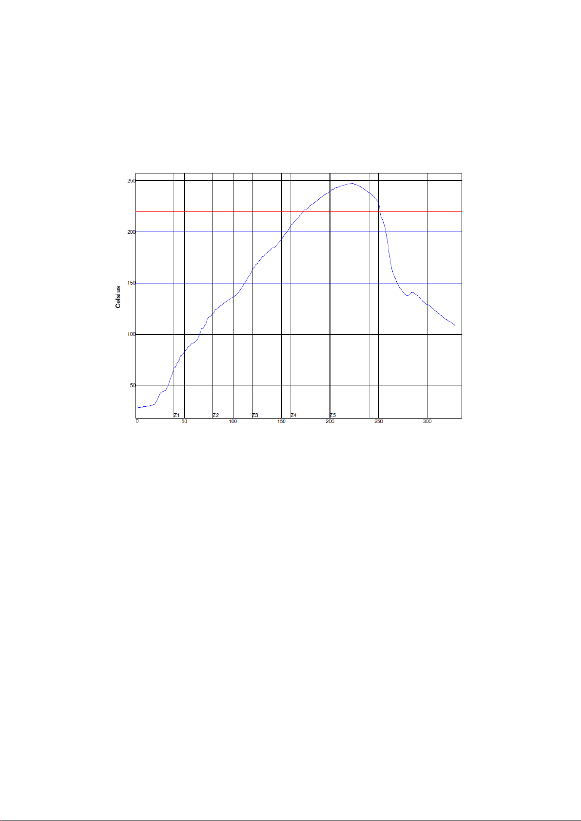
13.1 Soldering profile example
As an example of a typical soldering profile please see an example of a generic example of a reflow profile
shown below. As stated in previous section soldering profiles are solder paste specific. Consult the manufacturer
of the paste used.
Figure 25 Reference reflow profile example
Page 40

Silicon Labs 40
Tape and reel packaging
This section contains information regarding the tape and reel packaging and materials of packaging with
dimensions for the Bluegiga Bluetooth Dual Mode BT121 module.
14.1 Reel material and dimensions
• Reel material PS Conductive Black – surface resistance 103 ↔ 105
• Reel diameter 13”
• Reel color Black
Table 19 Reel dimensions
14.2 Tape material and dimensions
• Tape material PS Conductive Black – surface resistance 103 ↔ 105
Table 20 Tape dimensions
Symbol
Dimensions [mm]
D0
330.2
D1
100.0
W1
24.0
Symbol
Dimensions [mm]
P0
4.0
P1
16.0
D3
1.5
A0
11.3
B0
14.2
K0
2.7
W0
24.0 T 0.3
Page 41
Silicon Labs 41
14.3 Tape and reel box dimensions
Table 21 Tape and reel box dimensions
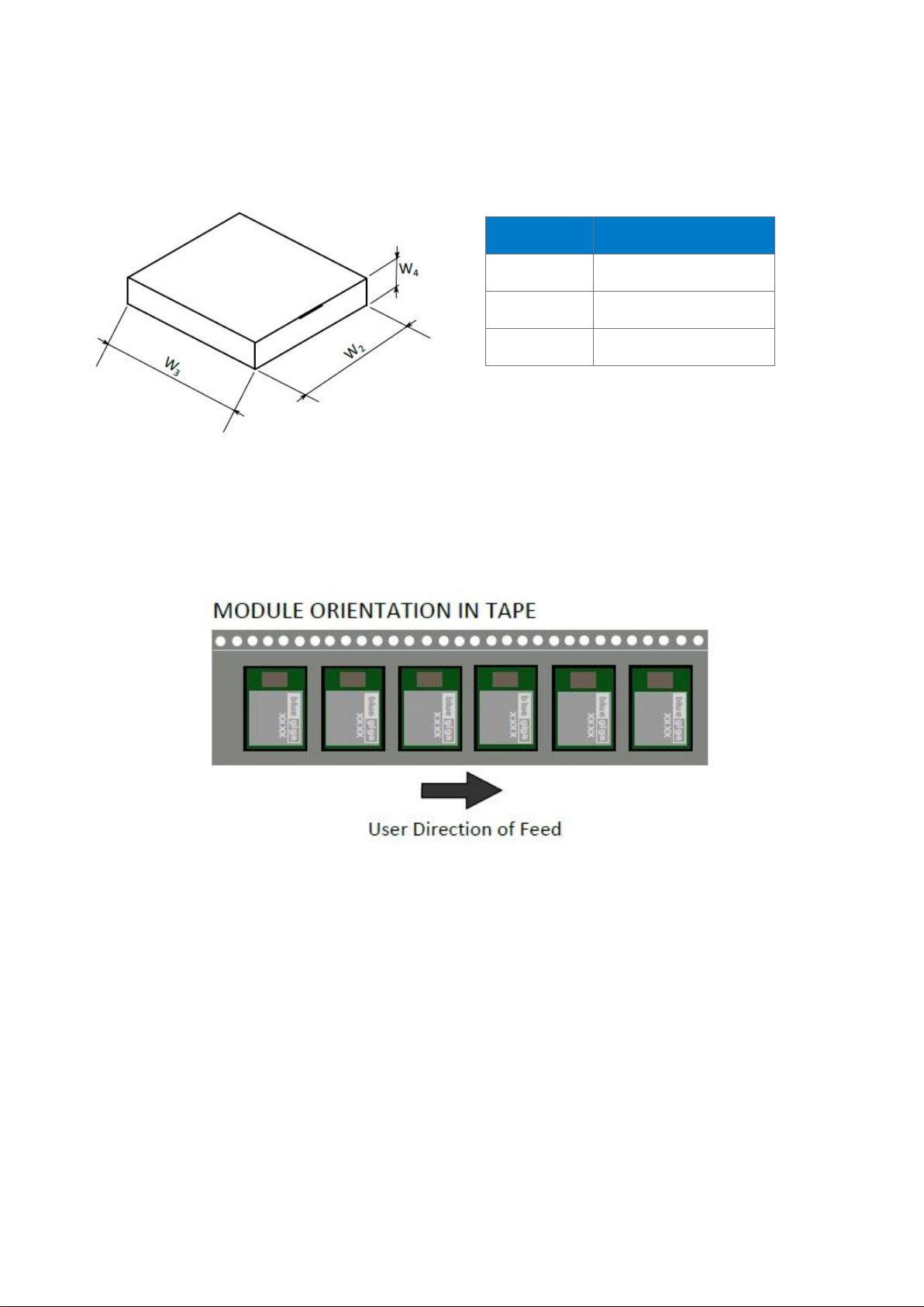
14.4 Module orientation in tape
Figure 26 Module orientation in tape and feed direction
Symbol
Dimensions [mm]
W1
338
W2
344
W3
44
Page 42

Silicon Labs 42
Certifications
15.1 Bluetooth
The Bluetooth declaration ID for BT121 hardware is: D027374
The Bluetooth declaration ID for Bluetooth Dual Mode software is: D027373
15.2 CE
The BT121 is tested against the relevant harmonized standards and is compliant with the essential requirements
and other relevant requirements of the Radio Equipment Directive (RED)(2014/53/EU).
Please notice that every end-product integrating the BT121 module will need to perform the radio EMC tests on
the end-product, according to EN 301 489-17. It is ultimately the responsibility of the manufacturer to ensure
the compliance of the end-product as a whole. The specific product assembly may have an impact to RF
radiated characteristics, and manufacturers should carefully consider RF radiated testing with the end-product
assembly.
The module is entitled to carry the CE mark, and a formal Declaration of Conformity (DoC) is available at the
product web page which is reachable starting from www.silabs.com.
15.3 FCC
This device complies with Part 15 of the FCC Rules. Operation is subject to the following two conditions:
(1) this device may not cause harmful interference, and
(2) this device must accept any interference received, including interference that may cause undesired
operation.
Any changes or modifications not expressly approved by Bluegiga Technologies could void the user’s authority
to operate the equipment.
FCC RF Radiation Exposure Statement:
This equipment complies with FCC radiation exposure limits set forth for an uncontrolled environment. End
users must follow the specific operating instructions for satisfying RF exposure compliance. This transmitter
meets both portable and mobile limits as demonstrated in the RF Exposure Analysis. This transmitter must not
be co-located or operating in conjunction with any other antenna or transmitter except in accordance with FCC
multi-transmitter product procedures.
As long as the condition above is met, further transmitter testing will not be required. However, the OEM
integrator is still responsible for testing their end-product for any additional compliance requirements required
with this module installed (for example, digital device emissions, PC peripheral requirements, etc.).
OEM Responsibilities to comply with FCC Regulations
The BT121 Module has been certified for integration into products only by OEM integrators under the following
conditions:
• The antenna(s) must be installed such that a minimum separation distance of 7 mm is maintained
between the radiator (antenna) and all persons at all times.
• The transmitter module must not be co-located or operating in conjunction with any other antenna or
transmitter except in accordance with FCC multi-transmitter product procedures.
Page 43

Silicon Labs 43
As long as the two conditions above are met, further transmitter testing will not be required. However, the OEM
integrator is still responsible for testing their end-product for any additional compliance requirements required
with this module installed (for example, digital device emissions, PC peripheral requirements, etc.).
IMPORTANT NOTE: In the event that these conditions cannot be met (for certain configurations or co-location
with another transmitter), then the FCC authorization is no longer considered valid and the FCC ID cannot be
used on the final product. In these circumstances, the OEM integrator will be responsible for re-evaluating the
end product (including the transmitter) and obtaining a separate FCC authorization.
End Product Labeling
The BT121 module is labeled with its own FCC ID. If the FCC ID is not visible when the module is installed
inside another device, then the outside of the device into which the module is installed must also display a label
referring to the enclosed module. In that case, the final end product must be labeled in a visible area with the
following:
“Contains Transmitter Module FCC ID: QOQBT121”
or
“Contains FCC ID: QOQBT121
The OEM integrator has to be aware not to provide information to the end user regarding how to install or
remove this RF module or change RF related parameters in the user manual of the end product.
15.4 IC
This radio transmitter (IC: 5123A-BGTBT121) has been approved by Industry Canada to operate with the
embedded chip antenna. Other antenna types are strictly prohibited for use with this device.
This device complies with Industry Canada’s license-exempt RSS standards. Operation is subject to the
following two conditions:
(1) This device may not cause interference; and
(2) This device must accept any interference, including interference that may cause undesired operation of the
device
RF Exposure Statement
Exception from routine SAR evaluation limits are given in RSS-102 Issue5. BT121 meets the given requirements
when the minimum separation distance to human body is less than equal to 20 mm. RF exposure or SAR
evaluation is not required when the separation distance is 20 mm or more. If the separation distance is less than
20 mm the OEM integrator is responsible for evaluating the SAR.
OEM Responsibilities to comply with IC Regulations
The BT121 Module has been certified for integration into products only by OEM integrators under the following
conditions:
• The antenna(s) must be installed such that a minimum separation distance of 20 mm is maintained
between the radiator (antenna) and all persons at all times.
• The transmitter module must not be co-located or operating in conjunction with any other antenna or
transmitter.
Page 44

Silicon Labs 44
As long as the two conditions above are met, further transmitter testing will not be required. However, the OEM
integrator is still responsible for testing their end-product for any additional compliance requirements required
with this module installed (for example, digital device emissions, PC peripheral requirements, etc.).
IMPORTANT NOTE: In the event that these conditions cannot be met (for certain configurations or co-location
with another transmitter), then the IC authorization is no longer considered valid and the IC ID cannot be used
on the final product. In these circumstances, the OEM integrator will be responsible for re-evaluating the end
product (including the transmitter) and obtaining a separate IC authorization
End Product Labeling
The BT121 module is labeled with its own IC ID. If the IC ID is not visible when the module is installed inside
another device, then the outside of the device into which the module is installed must also display a label
referring to the enclosed module. In that case, the final end product must be labeled in a visible area with the
following:
“Contains Transmitter Module IC: 5123A-BGTBT121”
or
“Contains IC: 5123A-BGTBT121
The OEM integrator has to be aware not to provide information to the end user regarding how to install or
remove this RF module or change RF related parameters in the user manual of the end product
15.4.1 IC (français)
Cet émetteur radio (IC : 5123A-BGTBT121) a reçu l'approbation d'Industrie Canada pour une exploitation avec
l'antenne puce incorporée. Il est strictement interdit d'utiliser d'autres types d'antenne avec cet appareil.
Le présent appareil est conforme aux CNR d’Industrie Canada applicables aux appareils radio exempts de
licence. L’exploitation est autorisée aux deux conditions suivantes :
1) l’appareil ne doit pas produire de brouillage;
2) l’utilisateur de l’appareil doit accepter tout brouillage radioélectrique subi, même si le brouillage est
susceptible d’en compromettre le fonctionnement.
Déclaration relative à l'exposition aux radiofréquences (RF)
Les limites applicables à l’exemption de l’évaluation courante du DAS sont énoncées dans le CNR 102, 5e
édition. L'appareil BT121 répond aux exigences données quand la distance de séparation minimum par rapport
au corps humain est inférieure ou égale à 20 mm. L'évaluation de l'exposition aux RF ou du DAS n'est pas
requise quand la distance de séparation est de 20 mm ou plus. Si la distance de séparation est inférieure à
20 mm, il incombe à l'intégrateur FEO d'évaluer le DAS.
Responsabilités du FEO ayant trait à la conformité avec les règlements IC
Le module BT121 a été certifié pour une intégration dans des produits uniquement par les intégrateurs FEO
dans les conditions suivantes :
• La ou les antennes doivent être installées de telle façon qu'une distance de séparation minimum de
20 mm soit maintenue entre le radiateur (antenne) et toute personne à tout moment.
• Le module émetteur ne doit pas être installé au même endroit ou fonctionner conjointement avec toute
autre antenne ou émetteur.
Page 45

Silicon Labs 45
Dès lors que les deux conditions ci-dessus sont respectées, d'autres tests de l'émetteur ne sont pas
obligatoires. Cependant, il incombe toujours à l'intégrateur FEO de tester la conformité de son produit final visà-vis de toute exigence supplémentaire avec ce module installé (par exemple, émissions de dispositifs
numériques, exigences relatives aux matériels périphériques PC, etc).
REMARQUE IMPORTANTE : S'il s'avère que ces conditions ne peuvent être respectées (pour certaines
configurations ou la colocation avec un autre émetteur), alors l'autorisation IC n'est plus considérée comme
valide et l'identifiant IC ne peut plus être employé sur le produit final. Dans ces circonstances, l'intégrateur FEO
aura la responsabilité de réévaluer le produit final (y compris l'émetteur) et d'obtenir une autorisation IC distincte.
Étiquetage du produit final
L'étiquette du module BT121 porte son propre identifiant IC. Si l'identifiant IC n'est pas visible quand le module
est installé à l'intérieur d'un autre appareil, l'extérieur de l'appareil dans lequel le module est installé doit aussi
porter une étiquette faisant référence au module qu'il contient. Dans ce cas, une étiquette comportant les
informations suivantes doit être collée sur une partie visible du produit final :
« Contient le module émetteur IC : 5123A-BGTBT121 »
ou
« Contient IC : 5123A-BGTBT121 »
L'intégrateur FEO doit être conscient de ne pas fournir d'informations à l'utilisateur final permettant d'installer
ou de retirer ce module RF ou de changer les paramètres liés aux RF dans le mode d'emploi du produit final.
15.5 MIC Japan
BT121 is certified in Japan with certification number 209-J00171.
Since September 1, 2014 it is allowed (and highly recommended) that a manufacturer who integrates a radio
module in their host equipment can place the certification mark and certification number (the same
marking/number as depicted on the label of the radio module) on the outside of the host equipment. The
certification mark and certification number must be placed close to the text in the Japanese language which is
provided below. This change in the Radio Law has been made in order to enable users of the combination of
host and radio module to verify if they are actually using a radio device which is approved for use in Japan.
当該機器には電波法に基づく、技術基準適合証明等を受けた特定無線設備を装着している。
Translation:
“This equipment contains specified radio equipment that has been certified to the Technical Regulation
Conformity Certification under the Radio Law.”
15.6 KC (South-Korea)
BT121 is certified in South-Korea with certification ID MSIP-CRM-BGT-BT121.
Page 46

Silicon Labs 46
Ordering information
Product code
Description
BT121-A-V2
BT121 Bluetooth Dual Mode module with an integrated antenna.
Mass production version.
BT121-A-V2-iAP
BT121 Bluetooth Dual Mode module with an integrated antenna and Apple
iAP profile. This part number is only available to Apple MFI licenses.
Mass production version.
BT121-A-V1
BT121 Bluetooth Dual Mode module with an integrated antenna
Engineering sample. Not recommended for new designs.
BT121-A-V1-iAP
BT121 Bluetooth Dual Mode module with an integrated antenna and Apple
iAP profile. This part number is only available to Apple MFI licenses.
Engineering sample. Not recommended for new designs.
DKBT
Bluegiga Bluetooth Dual Mode Development kit
Page 47

Simplicity Studio
One-click access to MCU and wireless
tools, documentation, software, source
code libraries & more. Available for
Windows, Mac and Linux!
IoT Portfolio
www.silabs.com/IoT
Disclaimer
Silicon Labs intends to provide customers with the latest, accurate, and in-depth documentation of all peripherals and modules available for system and software implementers using or
intending to use the Silicon Labs products. Characterization data, available modules and peripherals, memory sizes and memory addresses refer to each specific device, and “Typical”
parameters provided can and do vary in different applications. Application examples described herein are for illustrative purposes only. Silicon Labs reserves the right to make changes
without further notice to the product information, specifications, and descriptions herein, and does not give warranties as to the accuracy or completeness of the included information.
Without prior notification, Silicon Labs may update product firmware during the manufacturing process for security or reliability reasons. Such changes will not alter the specifications or
the performance of the product. Silicon Labs shall have no liability for the consequences of use of the information supplied in this document. This document does not imply or expressly
grant any license to design or fabricate any integrated circuits. The products are not designed or authorized to be used within any FDA Class III devices, applications for which FDA
premarket approval is required, or Life Support Systems without the specific written consent of Silicon Labs. A “Life Support System” is any product or system intended to support or
sustain life and/or health, which, if it fails, can be reasonably expected to result in significant personal injury or death. Silicon Labs products are not designed or authorized for military
applications. Silicon Labs products shall under no circumstances be used in weapons of mass destruction including (but not limited to) nuclear, biological or chemical weapons, or
missiles capable of delivering such weapons. Silicon Labs disclaims all express and implied warranties and shall not be responsible or liable for any injuries or damages related to use of
a Silicon Labs product in such unauthorized applications.
Trademark Information
Silicon Laboratories Inc.®, Silicon Laboratories®, Silicon Labs®, SiLabs® and the Silicon Labs logo®, Bluegiga®, Bluegiga Logo®, ClockBuilder®, CMEMS®, DSPLL®, EFM®,
EFM32®, EFR, Ember®, Energy Micro, Energy Micro logo and combinations thereof, “the world’s most energy friendly microcontrollers”, Ember®, EZLink®, EZRadio®, EZRadioPRO®,
Gecko®, Gecko OS, Gecko OS Studio, ISOmodem®, Precision32®, ProSLIC®, Simplicity Studio®, SiPHY®, Telegesis, the Telegesis Logo®, USBXpress®, Zentri, the Zentri logo and
Zentri DMS, Z-Wave®, and others are trademarks or registered trademarks of Silicon Labs. ARM, CORTEX, Cortex-M3 and THUMB are trademarks or registered trademarks of ARM
Holdings. Keil is a registered trademark of ARM Limited. Wi-Fi is a registered trademark of the Wi-Fi Alliance. All other products or brand names mentioned herein are trademarks of
their respective holders.
Silicon Laboratories Inc.
400 West Cesar Chavez
Austin, TX 78701
USA
http: //www.silabs.com
SW/HW
ww.silabs.com/simplicity
w
Quality
ww.silabs.com/quality
w
Support & Community
abs.com/community
www.sil
 Loading...