

Page 1
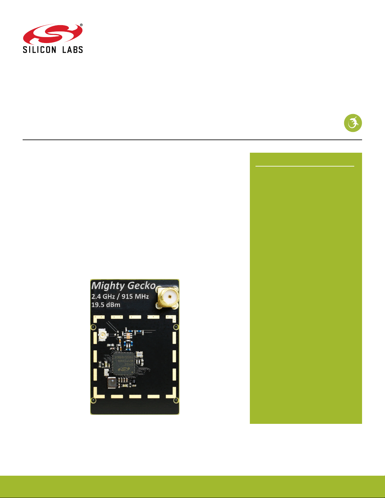
EFR32MG 2.4 GHz / 915 MHz Dual Band
19.5 dBm Radio Board
BRD4150B Reference Manual
The EFR32MG family of Wireless SoCs deliver a high performance, low energy wireless solution integrated into a small form
factor package.
By combining high performance sub-GHz RF and 2.4 GHz RF transceivers with an energy efficient 32-bit MCU, the family provides designers the ultimate in flexibility with a
family of pin-compatible devices that scale from 128/256 kB of flash and 16/32 kB of
RAM. The ultra-low power operating modes and fast wake-up times of the Silicon Labs
energy friendly 32-bit MCUs, combined with the low transmit and receive power consumption of the sub-GHz and 2.4 GHz radios result in a solution optimized for battery
powered applications.
To develop and/or evaluate the EFR32 Mighty Gecko the BRD4150B Radio Board can
be connected to the Wireless Starter Kit Mainboard to get access to display, buttons and
additional features from Expansion Boards.
RADIO BOARD FEATURES
• Wireless SoC:
EFR32MG1P233F256GM48
• CPU core: ARM Cortex-M4 with FPU
• Flash memory: 256 kB
• RAM: 32 kB
• Dual band transceiver integrated in the
Wireless SoC: EFR32
• Operation frequencies: 2.4 GHz
+ 915 MHz
• Transmit power: 19.5 dBm
• 2.4 GHz: Integrated PCB antenna.
• 915 MHz: Single SMA connector both for
transmit and receive
• Crystals for LFXO and HFXO: 32.768 kHz
and 38.4 MHz.
silabs.com | Smart. Connected. Energy-friendly. Rev. 1.00
Page 2

BRD4150B Reference Manual
Introduction
1. Introduction
The EFR32 Mighty Gecko Radio Boards provide a development platform (together with the Wireless Starter Kit Mainboard) for the
Silicon Labs EFR32 Mighty Gecko Wireless System on Chips and serve as reference designs for the matching networks of the RF interfaces.
The BRD4150B Radio Board supports dual-band operation with its integrated sub-GHz ISM band and 2.4 GHz band transceivers. The
sub-GHz section is designed to the operate in the US FCC 902-928 MHz band with an external whip antenna, the 2.4 GHz section is
designed to operate at the 2400-2483.5 MHz band with the on-board printed antenna. The matching networks are optimized to
19.5 dBm output power.
To develop and/or evaluate the EFR32 Mighty Gecko the BRD4150B Radio Board can be connected to the Wireless Starter Kit Mainboard to get access to display, buttons and additional features from Expansion Boards and also to evaluate the performance of the RF
interfaces.
silabs.com | Smart. Connected. Energy-friendly. Rev. 1.00 | 1
Page 3

GND
F9 / PA3 / VCOM.#RTS_#CS
3v3
NC / P36
P200
Upper Row
NC / P38
NC / P40
NC / P42
NC / P44
DEBUG.TMS_SWDIO / PF1 / F0
DISP_ENABLE / PD15 / F14
UIF_BUTTON0 / PF6 / F12
UIF_LED0 / PF4 / F10
VCOM.#CTS_SCLK / PA2 / F8
DEBUG.RESET / RADIO_#RESET / F4
DEBUG.TDO_SWO / PF2 / F2
DISP_SI / PC6 / F16
VCOM.TX_MOSI / PA0 / F6
PTI.DATA / PB12 / F20
DISP_EXTCOMIN / PD13 / F18
USB_VBUS
5V
Board ID SCL
GND
Board ID SDA
USB_VREG
F7 / PA1 / VCOM.RX_MISO
F5 / PA5 / VCOM_ENABLE
F3 / PF3 / DEBUG.TDI
F1 / PF0 / DEBUG.TCK_SWCLK
P45 / NC
P43 / NC
P41 / NC
P39 / NC
P37 / PD15 / SENSOR_ENABLE
F11 / PF5 / UIF_LED1
F13 / PF7 / UIF_BUTTON1
F15 / PC8 / DISP_SCLK
F17 / PD14 / DISP_SCS
F19 / PB13 / PTI.SYNC
F21 / PB11 / PTI.CLK
GND
VMCU_IN
VCOM.#CTS_SCLK / PA2 / P0
P201
Lower Row
VCOM.#RTS_#CS / PA3 / P2
UIF_BUTTON0 / PF6 / P4
UIF_BUTTON1 / PF7 / P6
GND
VRF_IN
P35 / PD15 / DISP_ENABLE
P7 / PC9
P5 / PC8 / DISP_SCLK
P3 / PC7
P1 / PC6 / DISP_SI
P33 / PD14 / DISP_SCS
P31 / PD13 / DISP_EXTCOMIN
P29 / NC
P27 / NC
P25 / NC
P23 / NC
P21 / NC
P19 / NC
P17 / NC
P15 / NC
P13 / PC11
P11 / PA1 /VCOM.RX_MISO
P9 / PA0 / VCOM.TX_MOSI
NC / P34
UIF_LED1 / PF5 / P32
NC / P30
DEBUG.TDO_SWO / PF2 / P28
DEBUG.TMS_SWDIO / PF1 / P26
DEBUG.TMS_SWCLK / PF0 / P24
PTI.SYNC / PB13 / P22
PTI.DATA / PB12 / P20
PTI.CLK / PB11 / P18
VCOM_ENABLE / PA5 / P16
PA4 / P14
PC10 / P12
DEBUG.TDI / PF3 / P10
UIF_LED0 / PF4 / P8
BRD4150B Reference Manual
Radio Board Connector
2. Radio Board Connector
2.1 Introduction
The board-to-board connector scheme allows access to all EFR32MG1 GPIO pins as well as the RESETn signal. For more information
on the functions of the available pin functions, we refer you to the EFR32MG1 Datasheet.
2.2 Radio Board Connector Pin Associations
The figure below shows the pin mapping on the connector to the radio pins and their function on the Wireless Starter Kit Mainboard.
silabs.com | Smart. Connected. Energy-friendly. Rev. 1.00 | 2
Figure 2.1. BRD4150B Radio Board Connector Pin Mapping
Page 4
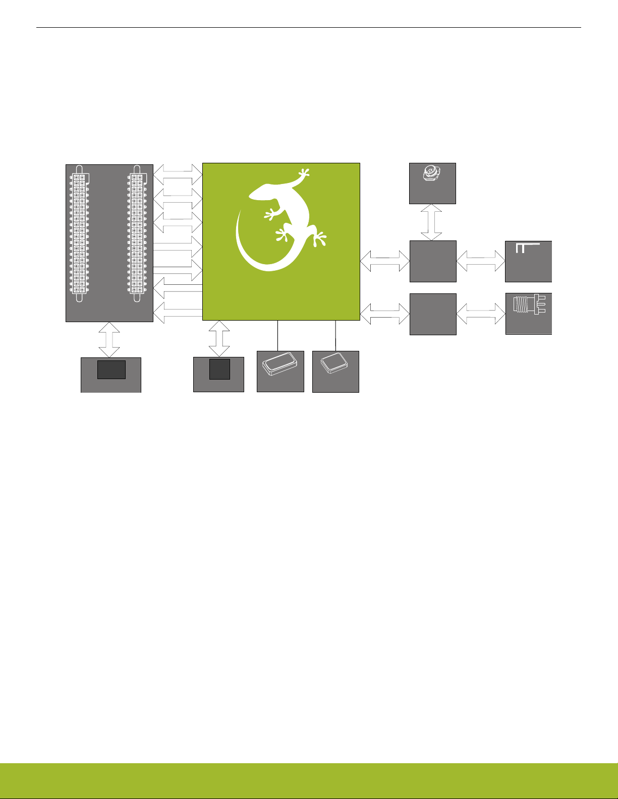
3. Radio Board Block Summary
EFR32
Inverted-F
PCB
Antenna
2.4 GHz RF
UFL
Connector
LF
Crystal
32.768k
HF
Crystal
38.4M
Radio
Board
Connectors
8 Mbit
MX25R
Serial Flash
I2C
24AA0024
Serial EEPROM
Matching
Network &
Path
Selection
GPIO
UART
Debug
Packet Trace
AEM
I2C
SPI
SPI
2.4 GHz RF
2.4 GHz RF
SubGHz RF
Matching
Network &
DC Bias
SubGHz RF
SMA
Connector
EFR32
EFR32
Wireless SoC
3.1 Introduction
This section gives a short introduction to the blocks of the BRD4150B Radio Board.
3.2 Radio Board Block Diagram
The block diagram of the BRD4150B Radio Board is shown in the figure below.
BRD4150B Reference Manual
Radio Board Block Summary
Figure 3.1. BRD4150B Block Diagram
3.3 Radio Board Block Description
3.3.1 Wireless MCU
The BRD4150B EFR32 Mighty Gecko Radio Board incorporates an EFR32MG1P233F256GM48 Wireless System on Chip featuring
32-bit Cortex-M4 with FPU core, 256 kB of flash memory 32 kB of RAM, an integrated 2.4 GHz band and an integrated sub-GHz ISM
band transceiver with output power up to 19.5 dBm. For additional information on the EFR32MG1P233F256GM48, refer to the
EFR32MG1 Data Sheet.
3.3.2 LF Crystal Oscillator (LFXO)
The BRD4150B Radio Board has a 32.768 kHz crystal mounted.
3.3.3 HF Crystal Oscillator (HFXO)
The BRD4150B Radio Board has a 38.4 MHz crystal mounted.
3.3.4 Matching Network for Sub-GHz
The BRD4150B Radio Board incorporates a sub-GHz matching network which connects both the sub-GHz TX and RX pins of the
EFR32MG1 to the one SMA connector to be able to transmit and receive with one antenna. The component values were optimized for
the 915 MHz band RF performace and current consumption with 19.5 dBm output power.
For detailed description of the matching network see Chapter 4.2.1 Description of the Sub-GHz RF Matching.
silabs.com | Smart. Connected. Energy-friendly. Rev. 1.00 | 3
Page 5

BRD4150B Reference Manual
Radio Board Block Summary
3.3.5 Matching Network for 2.4 GHz
The BRD4150B Radio Board incorporates a 2.4 GHz matching network which connects the 2.4 GHz TRX pin of the EFR32MG1 to the
one on-board printed Inverted-F antenna. The component values were optimized for the 2.4 GHz band RF performace and current consumption with 19.5 dBm output power.
For detailed description of the matching network see Chapter 4.2.2 Description of the 2.4 GHz RF Matching.
3.3.6 Inverted-F Antenna
The BRD4150B Radio Board includes a printed Inverted-F antenna (IFA) tuned to have close to 50 Ohm impedance at the 2.4 GHz
band.
For detailed description of the antenna see Chapter 4.6 Inverted-F Antenna.
3.3.7 SMA connector
To be able to perform conducted measurements or mount external antenna for radiated measurements, range tests etc., Silicon Labs
added an SMA connector to the Radio Board. The connector allows an external 50 Ohm cable or antenna to be connected during design verification or testing.
3.3.8 UFL Connector
To be able to perform conducted measurements Silicon Labs added an UFL connector to the Radio Board. The connector allows an
external 50 Ohm cable or antenna to be connected during design verification or testing.
Note: By default the output of the matching network is connected to the printed Inverted-F antenna by a series component. It can be
connected to the UFL connector as well through a series 0 Ohm resistor which is not mounted by default. For conducted measurements
through the UFL connector the series component to the antenna should be removed and the 0 Ohm resistor should be mounted (see
Chapter 4.2 Schematic of the RF Matching Network for further details).
3.3.9 Radio Board Connectors
Two dual-row, 0.05” pitch polarized connectors make up the BRD4150B Radio Board interface to the Wireless Starter Kit Mainboard.
For more information on the pin mapping between the EFR32MG1P233F256GM48 and the Radio Board Connector refer to Chapter
2.2 Radio Board Connector Pin Associations.
silabs.com | Smart. Connected. Energy-friendly. Rev. 1.00 | 4
Page 6
4. RF Section
GND
GND
GND
GND
VBIAS
GND
C1
C6
C10
L2
C3
C7
P2
U.FL
3
2
1
C4
Ground
RF I/ORF Crystal
RF Analog Power
PA Power
U1B
EFR32
2G4RF_IOP
20
2G4RF_ION
19
RFVDD
9
HFXI
10
HFXO
11
PAVDD
21
RFVSS
17
PAVSS
18
SUBGRF_OP
13
SUBGRF_ON
14
SUBGRF_IP
15
SUBGRF_IN
16
C8
C2
R2
0R
NM
L4
L6
TP1
R1
0R
L3
BAL1
0900BL15C050
SE
1
BAL2
4
BAL1
3
BIAS
2
GND
5
N/C
6
AT1
INVERTED_F
P1
SMA
3
2
1
4
5
L7
L1
L5
C5
Sub-GHz Matching Network
TRX Matching &
Filter
Filter
Antenna
Connector
Inverted-F
Antenna
Test
Connector
TRX Matching
Discrete Balun
2.4 GHz Matching Network
Path Selection
GND
GND
GND
VDCDC
VDCDC
GND
VBIAS
X1
38.400 MHz
31
2
4
C107
10P
L102
BLM18AG601SN1
1 2
L103
BLM18AG601SN1
1 2
C102
100P
C103
10P
C106
220N
Supply Filtering
High Frequency
Crystal
Sub-GHz PA
Power Supply
4.1 Introduction
This section gives a short introduction to the RF section of the BRD4150B.
4.2 Schematic of the RF Matching Network
The schematic of the RF section of the BRD4150B Radio Board is shown in the following figure.
BRD4150B Reference Manual
RF Section
Figure 4.1. Schematic of the RF Section of the BRD4150B
The RF matching comprises two separate TX/RX matching networks: one for the sub-GHz RF path, the other for the 2.4 GHz RF path.
4.2.1 Description of the Sub-GHz RF Matching
The sub-GHz matching network connects the differential TX outputs and RX inputs of the sub-GHz RF port to the SMA connector while
transforming the impedances to 50 Ohm. Careful design procedure was followed to ensure that the RX input circuitry does not load
down the TX output path while in TX mode and that the TX output circuitry does not degrade receive performance while in RX mode.
The matching includes a differential impedance matching circuitry, a discrete balanced-unbalanced transformer and a filter section. The
targeted output power is 19.5 dBm at 915 MHz.
4.2.2 Description of the 2.4 GHz RF Matching
The 2.4 GHz matching connects the 2G4RF_IOP pin to the on-board printed Inverted-F Antenna. The 2G4RF_ION pin is connected to
ground. For higher output powers (13 dBm and above) beside the impedance matching circuitry it is recommended to use additional
harmonic filtering as well at the RF output. The targeted output power of the BRD4150B board is 19.5 dBm thus the RF output of the IC
is connected to the antenna through a four-element impedance matching and harmonic filter circuitry.
For conducted measurements the output of the matching network can also be connected to the UFL connector by relocating the series
R1 0 Ohm resistor to the R2 position between the output of the matching and the UFL connector.
4.3 RF Section Power Supply
On the BRD4150B Radio Board the supply pin of the radio (RFVDD) is connected directly ot the output of the on-chip DC-DC converter
while the supply for the sub-GHz and 2.4 GHz power amplifiers (VBIAS) is provided directly by the Motherboard. This way, by default,
the DC-DC converter provides 1.8 V for the RF analog section, the Motherboard provides 3.3 V for the PAs (for details, see the schematic of the BRD4150B).
4.4 Bill of Materials for the sub-GHz Matching
The Bill of Materials of the sub-GHz matching network of the BRD4150B Radio Board is shown in the following table.
silabs.com | Smart. Connected. Energy-friendly. Rev. 1.00 | 5
Page 7
BRD4150B Reference Manual
RF Section
Table 4.1. Bill of Materials for the BRD4150B 915 MHz 19.5 dBm RF Matching Network
Component name Value Manufacturer Part Number
BAL1 Balun Johanson Technology 0900BL15C050
C3 1.8 pF Murata GRM1555C1H1R8WA01
C4 1.8 pF Murata GRM1555C1H1R8WA01
C5 3.9 pF Murata GRM1555C1H3R9WA01
C6 3.3 pF Murata GRM1555C1H3R3BA01
C7 5.6 pF Murata GRM1555C1H5R6BA01
C8 3.3 pF Murata GRM1555C1H3R3BA01
C10 56 pF Murata GRM1555C1H560GA01
L3 3.3 nH Murata LQW15AN3N3B80
L4 3.3 nH Murata LQW15AN3N3B80
L5 18 nH Murata LQW15AN18NG00
L6 10 nH Murata LQW15AN10NJ00
L7 10 nH Murata LQW15AN10NJ00
4.5 Bill of Materials for the 2.4 GHz Matching
The Bill of Materials of the 2.4 GHz matching network of the BRD4150B Radio Board is shown in the following table.
Table 4.2. Bill of Materials for the BRD4150B 2.4 GHz 19.5 dBm RF Matching Network
Component name Value Manufacturer Part Number
C1 2.0 pF Murata GRM1555C1H2R0WA01
C2 1.0 pF Murata GRM1555C1H1R0WA01
L1 1.8 nH Murata LQP15MN1N8W02
L2 3.0 nH Murata LQP15MN3N0W02
4.6 Inverted-F Antenna
The BRD4150B Radio Board includes an on-board printed Inverted-F Antenna tuned for the 2.4 GHz band. Due to the design restrictions of the Radio Board the input of the antenna and the output of the matching network can't be placed directly next to each other thus
a 50 Ohm transmission line was necessary to connect them. The resulting impedance and reflection measured at the output of the
matcing network are shown in the following figure. As it can be observed the impedance is close to 50 Ohm (the reflection is better than
-10 dB) for the entire 2.4 GHz band.
silabs.com | Smart. Connected. Energy-friendly. Rev. 1.00 | 6
Page 8

BRD4150B Reference Manual
RF Section
Figure 4.2. Impedance and Reflection of the Inverted-F Antenna of the BRD4150B
silabs.com | Smart. Connected. Energy-friendly. Rev. 1.00 | 7
Page 9

5. Mechanical Details
SMA Connector
LFXTAL
EFR32xx
HFXTAL
UFL
Connector
Printed
Inverted-F
Antenna
Sub-GHz RF
Matching
and Filter
Frame of
the
Optional
Shielding
Can
2.4 GHz Matching
and Filter
45 mm
30 mm
38.6 mm
4.4 mm
RF Output
Selection
DC-DC
&
Supply
Filter
Caps.
OTA
Flash
DC-DC
Inductor
24 mm
27.3 mm
28.6 mm
5 mm
Interface
Connector
Interface
Connector
15 mm
Board
Identification
PAVDD
Supply
Selection
Display
Enable
Selection
WSTK
Sensor
Enable
Selection
The BRD4150B EFR32 Mighty Gecko Radio Board is illustrated in the figures below.
BRD4150B Reference Manual
Mechanical Details
Figure 5.2. BRD4150B Bottom View
Figure 5.1. BRD4150B Top View
silabs.com | Smart. Connected. Energy-friendly. Rev. 1.00 | 8
Page 10

BRD4150B Reference Manual
EMC Compliance
6. EMC Compliance
6.1 Introduction
Compliance of the fundamental and harmonic levels is tested at the listed frequencies against the listed EMC regulations:
• 915 MHz:
• FCC 15.247
• 2.4 GHz:
• ETSI EN 300-328
• FCC 15.247
6.2 EMC Regulations for 915 MHz
6.2.1 FCC15.247 Emission Limits for the 902-928 MHz Band
FCC 15.247 allows conducted output power up to 1 Watt (30 dBm) in the 902-928 MHz MHz band. For spurious emmissions the limit is
-20 dBc based on either conducted or radiated measurement, if the emission is not in a restricted band. The restricted bands are specified in FCC 15.205. In these bands the spurious emission levels must meet the levels set out in FCC 15.209. In the range form
960 MHz to the frequency of the 10th harmonic it is defined as 0.5 mV/m at 3 m distance (equals to -41.2 dBm in EIRP).
In case of operating in the 902-928 MHz band from the first 10 harmonics only the 2nd and 7th harmonics don't fall into restricted bands
so for those the -20 dBc limit should be applied. For the rest of the harmonics the -41.2 dBm limit should be applied.
6.3 EMC Regulations for 2.4 GHz
6.3.1 ETSI EN 300-328 Emission Limits for the 2400-2483.5 MHz Band
Based on ETSI EN 300-328 the allowed maximum fundamental power for the 2400-2483.5 MHz band is 20 dBm EIRP. For the unwanted emissions in the 1 GHz to 12.75 GHz domain the specified limit is -30 dBm EIRP.
6.3.2 FCC15.247 Emission Limits for the 2400-2483.5 MHz Band
FCC 15.247 allows conducted output power up to 1 Watt (30 dBm) in the 2400-2483.5 MHz band. For spurious emmissions the limit is
-20 dBc based on either conducted or radiated measurement, if the emission is not in a restricted band. The restricted bands are specified in FCC 15.205. In these bands the spurious emission levels must meet the levels set out in FCC 15.209. In the range from
960 MHz to the frequency of the 5th harmonic it is defined as 0.5 mV/m at 3 m distance (equals to -41.2 dBm in EIRP).
Additionally, for spurious frequencies above 1 GHz FCC 15.35 allows duty-cycle relaxation to the regulatory limits. For the EmberZNet
PRO the relaxation is 3.6 dB. So practically the -41.2 dBm limit can be modified to -37.6 dBm.
In case of operating in the 2400-2483.5 MHz band the 2nd, 3rd and 5th harmonics can fall into restricted bands so for those the
-37.6 dBm limit should be applied. For the 4th harmonic the -20 dBc limit should be applied.
silabs.com | Smart. Connected. Energy-friendly. Rev. 1.00 | 9
Page 11

BRD4150B Reference Manual
EMC Compliance
6.3.3 Applied Emission Limits for the 2.4 GHz Band
The above ETSI limits are applied both for conducted and radiated measurements.
The FCC restricted band limits are radiated limits only. Besides that, Silicon Labs applies those to the conducted spectrum i.e. it is assumed that in case of a custom board an antenna is used which has 0 dB gain at the fundamental and the harmonic frequencies. In that
theoretical case, based on the conducted measurement, the compliance with the radiated limits can be estimated.
The overall applied limits are shown in the table below.
Table 6.1. Applied Limits for Spurious Emissions for the 2.4 GHz Band
Harmonic Frequency Limit
2nd 4800~4967 MHz -37.6 dBm
3rd 7200~7450.5 MHz -37.6 dBm
4th 9600~9934 MHz -30 dBm
5th 12000~12417.5 MHz -37.6 dBm
silabs.com | Smart. Connected. Energy-friendly. Rev. 1.00 | 10
Page 12

BRD4150B Reference Manual
RF Performance
7. RF Performance
7.1 Conducted Power Measurements
During measurements the BRD4150B Radio Board was attached to a Wireless Starter Kit Mainboard which was supplied by USB. The
voltage supply for the Radio Board was 3.3 V.
7.1.1 Conducted Measurements in the 915 MHz band
The BRD4150B Radio Board was connected directly to a Spectrum Analyzer through its SMA connector. The supply for the radio
(RFVDD) was 1.8 V provided by the on-chip DC-DC converter, the supply for the power amplifier (VBIAS) was 3.3 V provided by the
Motherboard (for details, see the schematic of the BRD4150B). The transceiver was operated in continuous carrier transmission mode.
The output power of the radio was set to 19.5 dBm.
The typical output spectrum is shown in the following figure.
Figure 7.1. Typical Output Spectrum of the BRD4150B
As it can be observed the fundamental is close to 19.5 dBm so it is compliant with the 30 dBm fundamental limit, the strongest unwanted emission is the double-frequency harmonic but with only around -44 dBm level it is compliant with the corresponding limit (-20 dBc)
with large margin. The other unwanted emissions are under the Spectrum Analyzer noise level (<-60 dBm). So the conducted spectrum
is compliant with the regulation limits.
silabs.com | Smart. Connected. Energy-friendly. Rev. 1.00 | 11
Page 13

BRD4150B Reference Manual
RF Performance
7.1.2 Conducted Measurements in the 2.4 GHz band
The BRD4150B Radio Board board was connected directly to a Spectrum Analyzer through its UFL connector (the 0 Ohm resistor was
removed from the R1 position and was soldered to the R2 position). The supply for the radio (RFVDD) was 1.8 V provided by the onchip DC-DC converter, the supply for the power amplifier (VBIAS) was 3.3 V provided by the Motherboard (for details, see the schematic of the BRD4150B). The transceiver was operated in continuous carrier transmission mode. The output power of the radio was set to
19.5 dBm.
The typical output spectrum is shown in the following figure.
Figure 7.2. Typical Output Spectrum of the BRD4150B
As it can be observed the fundamental is slightly lower than 19.5 dBm limit and the strongest unwanted emission is the double-frequency harmonic but with its -46.81 dBm level it is under the -37.6 dBm applied limit with ~9 dB margin. So the conducted spectrum is compliant with the applied limits.
Note: The conducted measurement is performed by connecting the on-board UFL connector to a Spectrum Analyzer through an SMA
Conversion Adapter (P/N: HRMJ-U.FLP(40)). This connection itself introduces approx. 0.3 dB insertion loss.
silabs.com | Smart. Connected. Energy-friendly. Rev. 1.00 | 12
Page 14

BRD4150B Reference Manual
RF Performance
7.2 Radiated Power Measurements
During measurements the BRD4150B Radio Board was attached to a Wireless Starter Kit Mainboard which was supplied by USB. The
voltage supply for the Radio Board was 3.3 V. The radiated power was measured in an antenna chamber by rotating the DUT in 360
degree with horizontal and vertical reference antenna polarizations in the XY, XZ and YZ cuts. The measurement axes are as shown in
the figure below.
Figure 7.3. DUT: Radio Board with the Wireless Starter Kit Mainboard (Illustration)
Note: The radiated measurement results presented in this document were recorded in an unlicensed antenna chamber. Also the radi-
ated power levels may change depending on the actual application (PCB size, used antenna etc.) therefore the absolute levels and
margins of the final application is recommended to be verified in a licensed EMC testhouse!
silabs.com | Smart. Connected. Energy-friendly. Rev. 1.00 | 13
Page 15

BRD4150B Reference Manual
RF Performance
7.2.1 Radiated Measurements in the 915 MHz band
For the 915 MHz radiated power measurements an external whip antenna (P/N: ANT-915-CW-HWR-SMA) was used as a transmitter
antenna. It was connected to the SMA connector of the BRD4150B Radio Board. The supply for the radio (RFVDD) was 1.8 V provided
by the on-chip DC-DC converter, the supply for the power amplifier (VBIAS) was 3.3 V provided by the Motherboard (for details, see the
schematic of the BRD4150B). The transceiver was operated in continuous carrier transmission mode. The output power of the radio
was set to 19.5 dBm.
The measured radiated powers are shown in the table below.
Table 7.1. Maximums of the Measured Radiated Powers of BRD4150B at 915 MHz
915 MHz EIRP [dBm] Orientation Margin [dB] Limit in EIRP [dBm]
Fundamental 20.0 YZ/H 10.0 30
2nd harmonic -33.5 XZ/H >30 -20 dBc
3rd harmonic -47.1 YZ/H 5.9 -41.2
4th harmonic -47.5 XZ/V 6.3 -41.2
5th harmonic
6th harmonic -45.8 YZ/V 4.6 -41.2
<-50
*
-/- >10 -41.2
7th harmonic -50.9 YZ/H >30 -20 dBc
8th harmonic -49.6 XZ/H 8.4 -41.2
9th harmonic
10th harmonic
<-50
<-50
*
*
-/- >10 -41.2
-/- >10 -41.2
* Signal level is below the Spectrum Analyzer noise floor.
As it can be observed the fundamental is below the regulation limit by 10 dB, the harmonic levels are also compliant.
7.2.2 Radiated Measurements in the 2.4 GHz band
For the 2.4 GHz radiated power measurements the on-board printed Inverted-F antenna of the BRD4150B Radio Board was used (the
R1 resistor was mounted). The supply for the radio (RFVDD) was 1.8 V provided by the on-chip DC-DC converter, the supply for the
power amplifier (VBIAS) was 3.3 V provided by the Motherboard (for details, see the schematic of the BRD4150B). The transceiver was
operated in continuous carrier transmission mode. The output power of the radio was set to 19.5 dBm. During the measurement the
sub-GHz antenna (P/N: ANT-915-CW-HWR-SMA) was attached to the SMA connector.
The results are shown in the table below.
Table 7.2. Maximums of the Measured Radiated Powers of BRD4150B at 2.4 GHz
2.4 GHz EIRP [dBm] Orientation Margin [dB] Limit in EIRP [dBm]
Fundamental 21.8 XY/H 8.2 30
2nd harmonic -45.0 YZ/V 7.4 -37.6
3rd harmonic
4th harmonic
5th harmonic
<-50
<-50
<-50
*
*
*
-/- >10 -37.6
-/- >20 -30
-/- >10 -37.6
* Signal level is below the Spectrum Analyzer noise floor.
As it can be observed, thanks to the ~2-3 dB gain of the on-board Inverted-F antenna, the level of the fundamental is higher than
19.5 dBm. The harmonic levels are comliant with the applied limits with large margins.
silabs.com | Smart. Connected. Energy-friendly. Rev. 1.00 | 14
Page 16

BRD4150B Reference Manual
EMC Compliance Recommendations
8. EMC Compliance Recommendations
8.1 Recommendations for 915 MHz FCC 15.247 compliance
As it was shown in the previous chapter the BRD4150B EFR32 Mighty Gecko Radio Board is compliant with the emission limits of the
FCC 15.247 regulation with 19.5 dBm output power. Although the BRD4150B Radio Board has an option for mounting a shielding can,
that is not required for the compliance.
8.2 Recommendations for 2.4 GHz ETSI EN 300-328 compliance
As it was shown in the previous chapter the radiated power of the fundamental of the BRD4150B EFR32 Mighty Gecko Radio Board
with 19.5 dBm output power exceeds the 20 dBm limit of the ETSI EN 300-328 regulation due to the high antenna gain so reduction of
the fundamental power is required by approx. 2 dB in order to comply. The harmonic emissions are under the -30 dBm limit with large
margin even with 19.5 dBm output power. Although the BRD4150B Radio Board has an option for mounting a shielding can, that is not
required for the compliance.
8.3 Recommendations for 2.4 GHz FCC 15.247 compliance
As it was shown in the previous chapter the BRD4150B EFR32 Mighty Gecko Radio Board is compliant with the emission limits of the
FCC 15.247 regulation with 19.5 dBm output power. Although the BRD4150B Radio Board has an option for mounting a shielding can,
that is not required for the compliance.
silabs.com | Smart. Connected. Energy-friendly. Rev. 1.00 | 15
Page 17

BRD4150B Reference Manual
Crystal Oscillator Tuning Parameters
9. Crystal Oscillator Tuning Parameters
The high frequency crystal oscillator (HFXO) requires proper settings to operate at the correct frequency. The crystal oscillator is designed to run at a nominal frequency of 38.4 MHz with the correct load capacitance. The EFR32 Mighty Gecko Wireless SoC has internal load capacitors that are configurable over a wide range. Changing the load capacitance is done by programming the correct c
value in the clock management unit (CMU).
The different revisions of radio boards that have been built have slight differences in the HFXO circuit, including external load capacitors
on some boards. Correct operation requires the correct c
value for your board revision. Please refer to the table below for details.
tune
Table 9.1. Ctune values for different board revisions
tune
PCB
Crystal Recommended
Revision
A00 NDK NX2016SA 38.4 MHz EXS00A-CS08568 CL =
8 pF (with external 10 pF load capacitors)
B00
KDS DSX211SH 38.4000 MHz CL = 10 pF 0x155 ~ -3 ppm. (Note that the crystal itself has a 10 ppm
and
above
Expected frequency offset with recommended
c
tune
value
c
tune
0 ~ -15 ppm (due to external load caps pulling outside
of c
range)
tune
rating at room temperature).
silabs.com | Smart. Connected. Energy-friendly. Rev. 1.00 | 16
Page 18

10. Document Revision History
Table 10.1. Document Revision History
Revision Number Effective Date Change Description
0.10 30.04.2015 Initial release
1.0 20.05.2015 Updated content for Rev C01 Radio Board.
BRD4150B Reference Manual
Document Revision History
silabs.com | Smart. Connected. Energy-friendly. Rev. 1.00 | 17
Page 19

11. Board Revisions
Table 11.1. BRD4150B Radio Board Revisions
Radio Board Revision Description
B00 Tuned PCB antenna and updated RF matching.
B01 Updated EFR32MG to Rev B0.
C00 Added serial flash. Updated matching network. Updated EFR32MG to Rev C0.
C01 Sub-GHz PA supplied from VBIAS (filtered PAVDD).
BRD4150B Reference Manual
Board Revisions
silabs.com | Smart. Connected. Energy-friendly. Rev. 1.00 | 18
Page 20

Table of Contents
1. Introduction ................................1
2. Radio Board Connector ...........................2
2.1 Introduction...............................2
2.2 Radio Board Connector Pin Associations.....................2
3. Radio Board Block Summary .........................3
3.1 Introduction...............................3
3.2 Radio Board Block Diagram .........................3
3.3 Radio Board Block Description ........................3
3.3.1 Wireless MCU .............................3
3.3.2 LF Crystal Oscillator (LFXO) ........................3
3.3.3 HF Crystal Oscillator (HFXO) ........................3
3.3.4 Matching Network for Sub-GHz .......................3
3.3.5 Matching Network for 2.4 GHz........................4
3.3.6 Inverted-F Antenna ...........................4
3.3.7 SMA connector .............................4
3.3.8 UFL Connector .............................4
3.3.9 Radio Board Connectors .........................4
4. RF Section ................................5
4.1 Introduction...............................5
4.2 Schematic of the RF Matching Network .....................5
4.2.1 Description of the Sub-GHz RF Matching ....................5
4.2.2 Description of the 2.4 GHz RF Matching ....................5
4.3 RF Section Power Supply ..........................5
4.4 Bill of Materials for the sub-GHz Matching ....................5
4.5 Bill of Materials for the 2.4 GHz Matching ....................6
4.6 Inverted-F Antenna ............................6
5. Mechanical Details .............................8
6. EMC Compliance ..............................9
6.1 Introduction...............................9
6.2 EMC Regulations for 915 MHz ........................9
6.2.1 FCC15.247 Emission Limits for the 902-928 MHz Band ...............9
6.3 EMC Regulations for 2.4 GHz ........................9
6.3.1 ETSI EN 300-328 Emission Limits for the 2400-2483.5 MHz Band ...........9
6.3.2 FCC15.247 Emission Limits for the 2400-2483.5 MHz Band..............9
6.3.3 Applied Emission Limits for the 2.4 GHz Band ..................10
7. RF Performance ..............................11
7.1 Conducted Power Measurements .......................11
7.1.1 Conducted Measurements in the 915 MHz band .................11
7.1.2 Conducted Measurements in the 2.4 GHz band ..................12
Table of Contents
19
Page 21

7.2 Radiated Power Measurements ........................13
7.2.1 Radiated Measurements in the 915 MHz band ..................14
7.2.2 Radiated Measurements in the 2.4 GHz band ..................14
8. EMC Compliance Recommendations ..................... 15
8.1 Recommendations for 915 MHz FCC 15.247 compliance ...............15
8.2 Recommendations for 2.4 GHz ETSI EN 300-328 compliance .............15
8.3 Recommendations for 2.4 GHz FCC 15.247 compliance ...............15
9. Crystal Oscillator Tuning Parameters ..................... 16
10. Document Revision History ........................ 17
11. Board Revisions............................. 18
Table of Contents .............................. 19
Table of Contents 20
Page 22

Simplicity Studio
One-click access to MCU and
wireless tools, documentation,
software, source code libraries &
more. Available for Windows,
Mac and Linux!
IoT Portfolio
www.silabs.com/IoT
Disclaimer
Silicon Laboratories intends to provide customers with the latest, accurate, and in-depth documentation of all peripherals and modules available for system and software implementers using
or intending to use the Silicon Laboratories products. Characterization data, available modules and peripherals, memory sizes and memory addresses refer to each specific device, and
"Typical" parameters provided can and do vary in different applications. Application examples described herein are for illustrative purposes only. Silicon Laboratories reserves the right to
make changes without further notice and limitation to product information, specifications, and descriptions herein, and does not give warranties as to the accuracy or completeness of the
included information. Silicon Laboratories shall have no liability for the consequences of use of the information supplied herein. This document does not imply or express copyright licenses
granted hereunder to design or fabricate any integrated circuits. The products are not designed or authorized to be used within any Life Support System without the specific written consent
of Silicon Laboratories. A "Life Support System" is any product or system intended to support or sustain life and/or health, which, if it fails, can be reasonably expected to result in significant
personal injury or death. Silicon Laboratories products are not designed or authorized for military applications. Silicon Laboratories products shall under no circumstances be used in
weapons of mass destruction including (but not limited to) nuclear, biological or chemical weapons, or missiles capable of delivering such weapons.
Trademark Information
Silicon Laboratories Inc.® , Silicon Laboratories®, Silicon Labs®, SiLabs® and the Silicon Labs logo®, Bluegiga®, Bluegiga Logo®, Clockbuilder®, CMEMS®, DSPLL®, EFM®, EFM32®,
EFR, Ember®, Energy Micro, Energy Micro logo and combinations thereof, "the world’s most energy friendly microcontrollers", Ember®, EZLink®, EZRadio®, EZRadioPRO®, Gecko®,
ISOmodem®, Precision32®, ProSLIC®, Simplicity Studio®, SiPHY®, T elegesis, the Telegesis Logo®, USBXpress® and others are trademarks or registered trademarks of Silicon Laboratories Inc. ARM, CORTEX, Cortex-M3 and THUMB are trademarks or registered trademarks of ARM Holdings. Keil is a registered trademark of ARM Limited. All other products or brand
names mentioned herein are trademarks of their respective holders.
Silicon Laboratories Inc.
400 West Cesar Chavez
Austin, TX 78701
USA
SW/HW
www.silabs.com/simplicity
Quality
www.silabs.com/quality
Support and Community
community.silabs.com
http://www.silabs.com
 Loading...