

Page 1
AN933.2: EFR32 Series 2 Minimal BOM
The purpose of this application note is to illustrate bill-of-material
(BOM)
and cost-optimized solutions for 2.4 GHz applications us-
ing the EFR32xG22 Wireless Gecko SoCs.
Silicon Labs reference radio board designs typically use an extensive number of components and multiple layers for RF and VDD filtering to achieve the best possible RF
performance at even the highest output power levels. So, the number of PCB layers
can be decreased and many of these elements can be eliminated from the design while
still maintaining an acceptable RF performance, especially at the lower power levels.
This document shows an absolute cost-optimized solution for the EFR32 Series 2 devices targeting high-volume and cost-sensitive applications, mainly applicable for Bluetooth Smart applications (i.e., BLE) at the 2.4 GHz frequency band, where the maximum allowed fundamental RF power is generally lower and the design is typically
space-constrained, such as for wearable applications. This application note includes
measured data with several different and simplified VDD filtering approaches at the 2.4
GHz frequency region. The RF front-end matching principles are described in more detail in the application note, AN930.2: EFR32 Series 2 2.4GHz Matching Guide. The RF
performance also strongly depends on the PCB layout as well as the design of the
matching networks. For optimal performance, Silicon Labs also recommends using the
PCB layout design guidelines described in the application note, AN928.2: EFR32 Ser-
ies 2 Layout Design Guide.
KEY POINTS
• BOM, cost, and PCB space-optimized
reference design for 2.4 GHz applications
•
Eliminates a number of components for
RF and VDD domains while maintaining
acceptable RF performance
• Measurement results for RX sensitivity, TX
performance, and harmonics are provided
silabs.com | Building a more connected world. Rev. 0.2
Page 2

1. Device Compatibility
This application note applies to the following EFR32 Series 2 devices:
•
EFR32BG22
• EFR32FG22
• EFR32MG22
AN933.2: EFR32 Series 2 Minimal BOM
Device Compatibility
silabs.com | Building a more connected world. Rev. 0.2 | 2
Page 3

AN933.2: EFR32 Series 2 Minimal BOM
Design Considerations
2. Design Considerations
This section summarizes the requirements and considerations for the BOM-optimized designs for EFR32xG22 devices.
• For
minimizing costs at the manufacturing level for EFR32xG22 devices, Silicon Labs designed a 2-layer reference design board for
customers to use as reference during their design phase. So, as an ultimate low cost solution, the minimal BOM solution presented
in this application note is also applicable to the 2-layer EFR32xG22 reference design. For the schematic, layout, BOM and other
design files of the low cost reference design, see the design package.
• EFR32 internal dc-dc converter is used for supplying the following VDD rails: DVDD, PAVDD, and RFVDD.
• The on-chip dc-dc converter needs an external inductor and capacitor for proper operation. The inductor used in the 2-layer reference design is CIG10W2R2MNC from Samsung, which is inexpensive and small, but can only be used for low load current. See
section 5. Recommendations for the DC-DC Converter’s External Inductor for other inductor options.
• For EFR32xG22, it is recommended to supply PAVDD, RFVDD, and DVDD from the on-chip dc-dc converter to achieve better current consumption (i.e., better power efficiency) and immunity against the battery voltage level drop and to avoid output power or RF
range degradation due to battery aging.
• For BLE 2.4 GHz applications, EFR32 needs to meet the BT Sleep Clock accuracy specification of ±500 ppm. EFR32xG22 has an
internal RC oscillator 32 kHz (LFRCO) with precision mode that meets the BLE requirements so an external low frequency crsytal
can be eliminated unless the application requires a higher clock accuracy. See section 4. Crystal Requirements if LFXO needs to be
used in the design.
• The high frequency XTAL is required for operation of RF and MCU parts of the EFR32. Load capacitors are not needed. See section
4. Crystal Requirements for the XTAL requirements.
• The RF front-end matching consists of a 3-element discrete LC structure that is needed to filter the harmonics and a dc blocking
capacitor.
• The following power supply restrictions need to be followed on the EFR32 Series 2 devices:
• VREGVDD ≥ DVDD
• DVDD ≥ DECOUPLE
• PAVDD ≥ RFVDD
• AVDD and IOVDD: No dependency with each other or any other supply pin
silabs.com | Building a more connected world. Rev. 0.2 | 3
Page 4
AN933.2: EFR32 Series 2 Minimal BOM
Recommended BOM-optimized 2.4 GHz Solution
3. Recommended BOM-optimized 2.4 GHz Solution
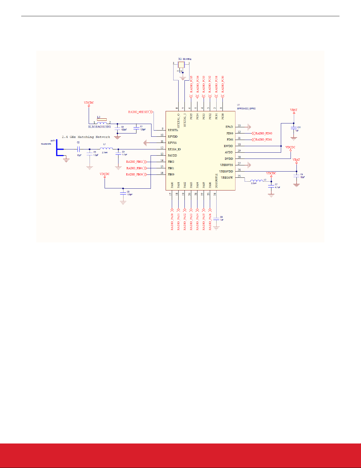
The recommended RF schematic for minimal BOM option for designs using EFR32xG22 wireless MCUs is shown in the figure below:
Figure 3.1. Minimal BOM 2.4 GHz Schematic for EFR32xG22
Note: C5 (120 pF) on PAVDD can be removed as well in designs using only the 0 dBm PA.
silabs.com | Building a more connected world. Rev. 0.2 | 4
Page 5

AN933.2: EFR32 Series 2 Minimal BOM
Recommended BOM-optimized 2.4 GHz Solution
3.1 Measured Performance Data
3.1.1 4-Layer EFR32xG22 Reference Design
full characterization was performed on Silicon Labs' reference radio board BRD4182A Rev. B05 to determine the minimal BOM solu-
A
tion without a significant compromise on the RF performance. For demonstration purposes and summarizing the test results, only a
subset of the measurements were chosen to share in this application note. The following measurements performed on BRD4182A are
based on the RF schematic shown in Figure 3.1 Minimal BOM 2.4 GHz Schematic for EFR32xG22 on page 4.
Table 3.1. Conducted RX Sensitivity
BLE PHY RFVDD Filtering RX Sensitivity (dBm)
Series Ferrite Parallel Capacitors
2 Mbps, 37 byte payload
1 Mbps, 37 byte payload
1
1
— 120 pF — -95.3
— 120 pF 100 nF -95.5
600R ferrite* 120 pF 100 nF -95.7
600R ferrite* 120 pF 100 nF -98.5
— 120 pF — -98.7
— 120 pF 100 nF -98.7
125kbps, 255 byte pay-
2
load
600R ferrite* 120 pF 100 nF -105.8
— 120 pF — -103.3
— 120 pF 100 nF -103.6
Note:
1.
0.1 % Bit Error Rate
2. 0.017% Bit Error Rate
PAVDD, RFVDD, and DVDD are connected to the on-chip dc-dc converter. AVDD, DVDD, IOVDD, and VREGVDD follow the filtering
configuration
provided in the minimal BOM schematic in Figure 3.1 Minimal BOM 2.4 GHz Schematic for EFR32xG22 on page 4. There
is no filtering on PAVDD.
The conducted RX sensitivity was checked with BLE packets at various data rates (2Mbps, 1 Mbps, and 125 kbps) and the values are
provided here mainly for comparison purposes between the different RFVDD filtering cases. The table above demonstrates that the
lack of filtering on RFVDD can cause up to 2 dB of degradation in sensitivity. The best performer of these minimal BOM configurations
is marked with an asterisk "*".
silabs.com | Building a more connected world. Rev. 0.2 | 5
Page 6

Recommended BOM-optimized 2.4 GHz Solution
Table 3.2. Radiated TX Power and Harmonics
AN933.2: EFR32 Series 2 Minimal BOM
PA BOM Configu-
ration
1
Capacitor on
PAVDD
TX Power @
2440 MHz
H2 max (dBm) H3 max (dBm) H4 max (dBm) H5 max (dBm)
(dBm)
0 dBm
6 dBm No 8.2 -55.4 -36.8
Optimized
No 2.4 -54.3 -49.4
6 dBm* Yes 8.8 -56.1 -37.6
6 dBm Default N/A 8.7 -55.7 -38.4
< -51.6
< -51.9
< -51.9
< -52.3
2
2
2
2
< -48.7
-33.3
-36.1
-37
2
Note:
1.
The default BOM configuration refers to the full BOM on the reference design. The optimized BOM refers to the minimal BOM
solution from the schematic shown in Figure 3.1 Minimal BOM 2.4 GHz Schematic for EFR32xG22 on page 4 except for PAVDD
where the TX measurements are taken with and without a 120 pF capacitor.
2. Under SA noise floor.
Although no filtering is required on PAVDD for acceptable RX sensitivity as shown in Table 3.1 Conducted RX Sensitivity on page 5, a
120 pF on PAVDD is needed for the radiated TX harmonic levels to achieve similar performance as the default BOM configuration with
~1dB difference. So, this configuration is the best minimal BOM configuration as marked by the asterisk "*".
The harmonic values are the measured maximums of the radiated power in EIRP (dBm) taken in an unmodulated carrier transmission
mode so depending on the modulation scheme, the actual radiated power with modulated transmission will be lower. The calculated
modulated EIRP of the best performer of the BOM configurations is provided in Table 3.3 below, which shows that the critical 3rd and
5th harmonics are indeed compliant with FCC/ETSI limits. The modulation scheme with the lowest correction factor was chosen for the
calculations to show the worst case margins. See the BRD4182A reference manual for more details on the measured relaxation factors
of the supported modulation schemes to calculate the modulated EIRP from the measured unmodulated EIRP.
Table 3.3. Calculated Modulated EIRP
Frequency (2440
MHz)
Measured Unmodu-
lated EIRP (dBm)
BLE 125 Kb/s Coded Modulation Limit in EIRP (dBm)
Correction Factor
(dB)
Calculated Modula-
ted EIRP (dBm)
Modulated Margin
(dB)
Fund 8.8 N/A 8.8 21.2 30
2nd -56.1 -2.7 -58.8 17.6 -41.2
3rd -37.6 -4.8 -42.4 1.2 -41.2
4th <-51.9 -5.5 <-57.4 27.4 -30
5th -36.1 -6.3 -42.4 1.2 -41.2
silabs.com | Building a more connected world. Rev. 0.2 | 6
Page 7

AN933.2: EFR32 Series 2 Minimal BOM
Recommended BOM-optimized 2.4 GHz Solution
3.1.2 2-Layer EFR32xG22 Reference Design
following conducted and radiated measurements show that the minimal BOM solution determined for BRD4182A is applicable to
The
the low-cost, 2-layer EFR32xG22 reference design as well due to the similar performance with default vs. optimized BOM.
Table 3.4. Conducted TX Power, Harmonics, and RX Sensitivity
BOM Configuration Frequency
(MHz)
Power Lev-
el (raw)
RX Sensitivi-
ty (dBm)
TX Power
(dBm)
H2 max
(dBm)
H3 max
(dBm)
H4 max
(dBm)
H5 max
(dBm)
Default 2450 52 -97.9 6.2 -68 -35 -56 -42
2450 52 -97.8 6 -65 -36 -56 -43
2405 114 -97.4 8.2 -57 -32 -54 -37
Optimized
2450 114 -97.8 8.1 -60 -33 -53 -35
2478 114 -96.8 8.05 -61 -33 -53 -35
Note:
1.
BOM optimized solution provided in Figure 3.1 Minimal BOM 2.4 GHz Schematic for EFR32xG22 on page 4 was used for the
measurements.
2. RX Sensitivity test condition: BLE PHY 1 Mbps 2GFSK, 0.1 % BER.
3. The conducted harmonic levels were measured using an unmodulated carrier tone.
As shown in the table above, the 2-layer board can transmit up to 8 dBm; however, the 3rd and 5th harmonic performance degrades
significantly, so the recommended minimal BOM solution can be applied to power levels up to 6 dBm.
Table 3.5. Radiated TX Power and Harmonics
BOM Configuration Frequency (MHz) TX Power @ 2440 MHz
H2 max (dBm) H3 max (dBm) H4 max (dBm) H5 max (dBm)
1
(dBm)
Optimized 2449 5.8 -50.18 -37.45 -50.9 -42.31
Default 2449 5.38 -48.44 -37.91 -50.93 -43.92
Note:
1.
Tested at 6 dBm power level (52 raw).
The data shows that the radiated performance is within ~1 dB difference between the optimized and the default BOM, so the optimized
solution provided in Figure 3.1 Minimal BOM 2.4 GHz Schematic for EFR32xG22 on page 4 can be used on 2-layer EFR32xG22
BOM
designs.
The harmonic values are the measured maximums of the radiated power in EIRP (dBm) taken in an unmodulated carrier transmission
mode, so the true evaluation of the radiated harmonics compliance with ETSI/FCC limits is done in Table 3.6 Calculated Modulated
EIRP on page 8, which shows that the critical 3rd harmonic passes the regulatory limits with a 1.05 dB margin.
silabs.com | Building a more connected world. Rev. 0.2 | 7
Page 8
Recommended BOM-optimized 2.4 GHz Solution
Table 3.6. Calculated Modulated EIRP
AN933.2: EFR32 Series 2 Minimal BOM
Frequency (2440
MHz)
Measured Unmodulated
EIRP (dBm)
BLE 125 Kb/s Coded Modulation Limit in EIRP
Correction Factor
(dB)
Calculated Modu-
lated EIRP (dBm)
Modulated Mar-
gin (dB)
(dBm)
Fund 5.8 N/A 5.8 24.2 30
2nd -50.18 -2.7 -52.88 11.68 -41.2
3rd -37.45 -4.8 -42.25 1.05 -41.2
4th -50.9 -5.5 -56.4 26.4 -30
5th -42.31 -6.3 -48.61 7.41 -41.2
3.2 Additional Concerns
section lists some additional concerns regarding the RF performance versus different BOM options, and provides some further
This
suggestions on the space constraint layout designs.
• If the on-chip dc-dc converter is not used, the following components can be eliminated from the schematic shown in Figure
3.1 Minimal BOM 2.4 GHz Schematic for EFR32xG22 on page 4: L2 and C7. However, the trade-off would be an increase in current
consumption. Refer to Section 4.6 of EFR32xG22's data sheet for more details on the current consumption values in different EM
modes.
• Because the AVDD and IOVDD pads are beside each other, a single 1 uF capacitor can be used for both VDD supplies; however,
they must be tied together.
• Even in space-constrained designs, it is strongly recommended to place the L2 and C7 components (at the on-chip dc-dc converter
output) as close to the EFR32xG22 wireless MCU’s VREGSW pin as possible. Also, the L2 dc-dc inductor should be placed far
away from any noise-sensitive circuitry (ex: radio antenna).
• The high frequency crystal also needs to be placed close to the EFR32xG22 wireless MCU.
• A 100 nF capacitor on the RESET line is needed to filter noise if the trace is long and routed to a push button on a different board.
Otherwise, it can be eliminated.
• The critical harmonics, such as the 3rd and 5th harmonic, are sensitive to the routing of the RF path from the chip to the antenna, so
it is strongly recommended to follow the layout approach provided in AN928.2: EFR32 Series 2 Layout Design Guide for achieving
optimal RF performance.
silabs.com | Building a more connected world. Rev. 0.2 | 8
Page 9

AN933.2: EFR32 Series 2 Minimal BOM
Crystal Requirements
4. Crystal Requirements
Table 4.1. Crystal Requirements
XTAL Type Crystal Frequency Gain ESR Load Capacitance
Typ Max Min Typ Max
LFXO 32.768 kHz 0 —
1 — 100 kΩ 6 — 10
2 — 10 — 12.5
3 — 12.5 — 18
HFXO 38.4 MHz — 40 Ω — — 10 pF —
Note:
1.
Many applications do not require the use of an external LFXO. With the EFR32xG22, there is a LFRCO with precision mode (32
kHz with 500 ppm accuracy), which can replace the external LFXO component in many use cases. Many applications do not require precise sleep timing and can operate with the LFRCO (32 kHz) or even the ULFRCO (1 kHz), again eliminating the need for
an external LFXO.
80 kΩ
1
4 — 6
silabs.com | Building a more connected world. Rev. 0.2 | 9
Page 10

AN933.2: EFR32 Series 2 Minimal BOM
Recommendations for the DC-DC Converter’s External Inductor
5. Recommendations for the DC-DC Converter’s External Inductor
• Silicon Labs' general recommendation on the external inductor for the internal dc-dc converter is to use the CIG22H2R2MNE from
Samsung which has very good performance and is inexpensive, but a bit large (2.5 x 2 mm) compared to CIG10W2R2MNC (1.6 x
0.8 mm).
• Some additional candidates: LQM2HPN2R2MG0L, CIG22L2R2MNE
silabs.com | Building a more connected world. Rev. 0.2 | 10
Page 11

6. Revision History
Revision 0.2
November, 2020
•
Updated minimal BOM recommendation to be applicable to the 6 dBm PA.
• Added test results of minimal BOM testing on radio board BRD4182A.
• Updated test results of EFR32xG22 2-layer reference design.
Revision 0.1
March, 2020
• Initial release.
AN933.2: EFR32 Series 2 Minimal BOM
Revision History
silabs.com | Building a more connected world. Rev. 0.2 | 11
Page 12

Simplicity Studio
One-click access to MCU and wireless
tools, documentation, software, source
code libraries & more. Available for
Windows, Mac and Linux!
IoT Portfolio
www.silabs.com/IoT
Disclaimer
Silicon Labs intends to provide customers with the latest, accurate, and in-depth documentation of all peripherals and modules available for system and software implementers using or
intending to use the Silicon Labs products. Characterization data, available modules and peripherals, memory sizes and memory addresses refer to each specific device, and “Typical”
parameters provided can and do vary in different applications. Application examples described herein are for illustrative purposes only. Silicon Labs reserves the right to make changes
without further notice to the product information, specifications, and descriptions herein, and does not give warranties as to the accuracy or completeness of the included information.
Without prior notification, Silicon Labs may update product firmware during the manufacturing process for security or reliability reasons. Such changes will not alter the specifications or
the performance of the product. Silicon Labs shall have no liability for the consequences of use of the information supplied in this document. This document does not imply or expressly
grant any license to design or fabricate any integrated circuits. The products are not designed or authorized to be used within any FDA Class III devices, applications for which FDA
premarket approval is required, or Life Support Systems without the specific written consent of Silicon Labs. A “Life Support System” is any product or system intended to support or
sustain life and/or health, which, if it fails, can be reasonably expected to result in significant personal injury or death. Silicon Labs products are not designed or authorized for military
applications. Silicon Labs products shall under no circumstances be used in weapons of mass destruction including (but not limited to) nuclear, biological or chemical weapons, or
missiles capable of delivering such weapons. Silicon Labs disclaims all express and implied warranties and shall not be responsible or liable for any injuries or damages related to use of
a Silicon Labs product in such unauthorized applications.
Trademark Information
Silicon Laboratories Inc.®, Silicon Laboratories®, Silicon Labs®, SiLabs® and the Silicon Labs logo®, Bluegiga®, Bluegiga Logo®, ClockBuilder®, CMEMS®, DSPLL®, EFM®,
EFM32®, EFR, Ember®, Energy Micro, Energy Micro logo and combinations thereof, “the world’s most energy friendly microcontrollers”, Ember®, EZLink®, EZRadio®, EZRadioPRO®,
Gecko®, Gecko OS, Gecko OS Studio, ISOmodem®, Precision32®, ProSLIC®, Simplicity Studio®, SiPHY®, Telegesis, the Telegesis Logo®, USBXpress®, Zentri, the Zentri logo and
Zentri DMS, Z-Wave®, and others are trademarks or registered trademarks of Silicon Labs. ARM, CORTEX, Cortex-M3 and THUMB are trademarks or registered trademarks of ARM
Holdings. Keil is a registered trademark of ARM Limited. Wi-Fi is a registered trademark of the Wi-Fi Alliance. All other products or brand names mentioned herein are trademarks of
their respective holders.
Silicon Laboratories Inc.
400 West Cesar Chavez
Austin, TX 78701
USA
http: //www.silabs.com
SW/HW
w.silabs.com/simplicity
ww
Quality
w.silabs.com/quality
ww
Support & Community
www.silabs.com/community
 Loading...