

Page 1

Si8410/20/21
LOW-POWER SINGLE AND DUAL-CHANNEL
D
IGITAL ISOLATORS
Features
High-speed operation
DC to 150 Mbps
No start-up initialization required
Wide Operating Supply Voltage:
2.70–5.5 V
Ultra low power (typical)
5 V Operation:
< 2.1 mA per channel at 1 Mbps
< 6 mA per channel at 100 Mbps
2.70 V Operation:
< 1.8 mA per channel at 1 Mbps
< 4 mA per channel at 100 Mbps
High electromagnetic immunity
Applications
Industrial automation systems
Hybrid electric vehicles
Isolated switch mode supplies
Safety Regulatory Approvals
UL 1577 recognized
Up to 2500 V
CSA component notice 5A
approval
IEC 60950-1, 61010-1
(reinforced
for 1 minute
RMS
Not Recommended
insulation)
Up to 2500 V
60-year life at rated working
voltage
Precise timing (typ ica l)
<10 ns worst case
1.5 ns pulse width distortion
0.5 ns channel-channel skew
2 ns propagation delay skew
6 ns minimum pulse width
Transient Immunity 25 kV/µs
Wide temperature range
–40 to 125 °C at 150 Mbps
RoHS-compliant packages
SOIC-8 narrow body
Isolated ADC, DAC
Motor control
Power inverters
Communications systems
RMS
isolation
w
e
VDE certification conformity
IEC 60747-5-2
(VDE0884 Part 2)
r N
o
f
e
D
g
si
s
n
Ordering Information:
See page 25.
Description
Silicon Lab's family of ultra-low-power digital isolators are CMOS devices
offering substantial data rate, propagation delay, power, size, reliability,
and external BOM advantages when compared to legacy isolation
technologies. The operating parameters of these products remain stable
across wide temperature rang es through out their service life. For ease of
design, only VDD bypass capacitors are required.
Data rates up to 150 Mbps are supported, and all devices achieve worstcase propagation delays of less than 10 ns. All products are safety
certified by UL, CSA, and VDE and support withstand voltages of up to
2.5 kVrms. These devices are available in an 8-pin narrow-body SOIC
package.
Rev. 1.5 9/13 Copyright © 2013 by Silicon Laboratories Si8410/20/21
Page 2

Si8410/20/21
s
n
g
si
e
D
w
e
r N
Not Recommended
o
f
2 Rev. 1.5
Page 3

Si8410/20/21
TABLE OF CONTENTS
Section Page
1. Electrical Specifications . . . . . . . . . . . . . . . . . . . . . . . . . . . . . . . . . . . . . . . . . . . . . . . . . . .4
2. Functional Description . . . . . . . . . . . . . . . . . . . . . . . . . . . . . . . . . . . . . . . . . . . . . . . . . . .17
2.1. Theory of Operation . . . . . . . . . . . . . . . . . . . . . . . . . . . . . . . . . . . . . . . . . . . . . . . . .17
2.2. Eye Diagram . . . . . . . . . . . . . . . . . . . . . . . . . . . . . . . . . . . . . . . . . . . . . . . . . . . . . . .18
2.3. Device Operation . . . . . . . . . . . . . . . . . . . . . . . . . . . . . . . . . . . . . . . . . . . . . . . . . . .19
2.4. Layout Recommendations . . . . . . . . . . . . . . . . . . . . . . . . . . . . . . . . . . . . . . . . . . . .20
2.5. Typical Performance Characteristics . . . . . . . . . . . . . . . . . . . . . . . . . . . . . . . . . . . .21
3. Errata and Design Migration Guidelines . . . . . . . . . . . . . . . . . . . . . . . . . . . . . . . . . . . . .23
3.1. Power Supply Bypass Capacitors (Revision C and Revision D) . . . . . . . . . . . . . . . .23
3.2. Latch Up Immunity (Revision C Only) . . . . . . . . . . . . . . . . . . . . . . . . . . . . . . . . . . . .23
4. Pin Descriptions . . . . . . . . . . . . . . . . . . . . . . . . . . . . . . . . . . . . . . . . . . . . . . . . . . . . . . . . .24
5. Ordering Guide . . . . . . . . . . . . . . . . . . . . . . . . . . . . . . . . . . . . . . . . . . . . . . . . . . . . . . . . . .25
6. Package Outline: 8-Pin Narrow Body SOIC . . . . . . . . . . . . . . . . . . . . . . . . . . . . . . . . . . .26
7. Land Pattern: 8-Pin Narrow Body SOIC . . . . . . . . . . . . . . . . . . . . . . . . . . . . . . . . . . . . . .27
8. Top Marking: 8-Pin Narrow Body SOIC . . . . . . . . . . . . . . . . . . . . . . . . . . . . . . . . . . . . . .28
8.1. 8-Pin Narrow Body SOIC Top Marking . . . . . . . . . . . . . . . . . . . . . . . . . . . . . . . . . . .28
8.2. Top Marking Explanation . . . . . . . . . . . . . . . . . . . . . . . . . . . . . . . . . . . . . . . . . . . . .28
Document Change List . . . . . . . . . . . . . . . . . . . . . . . . . . . . . . . . . . . . . . . . . . . . . . . . . . . . .29
Contact Information . . . . . . . . . . . . . . . . . . . . . . . . . . . . . . . . . . . . . . . . . . . . . . . . . . . . . . . .30
e
g
si
s
n
D
w
e
r N
Not Recommended
o
f
Rev. 1.5 3
Page 4

Si8410/20/21
1. Electrical Specifications
Table 1. Recommended Operating Conditions
Parameter Symbol Test Condition Min Typ Max Unit
Ambient Operating Temperature* T
Supply Voltage V
*Note: The maximum ambient temperatur e is dependent upon data frequency, output loading, the number of operating
channels, and supply voltage.
Table 2. Absolute Maximum Ratings
Parameter Symbol Min Typ Max Unit
Storage Temperature
Operating Temperature T
Supply Voltage (Revision C)
Supply Voltage (Revision D)
Input Voltage V
Output Voltage V
Output Current Drive Channel I
Lead Solder Temperature (10 s) — — 260 °C
Maximum Isolation Voltage (1 s) — — 3600 V
Notes:
1. Permanent device damage may occur if the absolute maximum ratings are exceeded. Functional operation should be
restricted to conditions as specified in the operational sections of this data sheet.
2. VDE certifies storage temperature from –40 to 150 °C.
3. See "5. Ordering Guide" on page 25 for more information.
2
3
3
V
A
DD1
DD2
150 Mbps, 15 pF, 5 V –40 25 125 °C
2.70 — 5.5 V
2.70 — 5.5 V
1
V
V
T
DD1
DD1
STG
A
, V
, V
I
O
O
DD2
DD2
–65 — 150 °C
–40 — 125 °C
–0.5 — 5.75 V
–0.5 — 6.0 V
s
n
g
–0.5 — VDD + 0.5 V
si
–0.5 — VDD + 0.5 V
——10mA
e
D
w
e
RMS
Not Recommended
r N
o
f
4 Rev. 1.5
Page 5

Si8410/20/21
Table 3. Electrical Characteristics
(V
= 5 V ±10%, V
DD1
Parameter Symbol Test Condition Min Typ Max Unit
High Level Input Volt age V
Low Level Input Voltage V
High Level Output Voltage V
Low Level Output Voltage V
Input Leakage Current I
Output Impedance
Si8410Ax, Bx
V
DD1
V
DD2
V
DD1
V
DD2
Si8420Ax, Bx
V
DD1
V
DD2
V
DD1
V
DD2
Si8421Ax, Bx
V
DD1
V
DD2
V
DD1
V
DD2
1 Mbps Supply Current (All inputs= 500 kHz square wave, CI = 15 pF on all outputs)
Si8410Ax, Bx
V
DD1
V
DD2
Si8420Ax, Bx
V
DD1
V
DD2
Si8421Ax, Bx
V
DD1
V
DD2
Notes:
1. The nominal output impedance of an isolator driver channel is approximately 85 , ±40%, which is a combination of
the value of the on-chip series termination resistor and channel resistance of the output driver FET . When driving loads
where transmission line effects will be a factor, output pins should be appropriately terminated with controlled
impedance PCB traces.
2. t
PSK(P-P)
the same supply voltages, load, and ambient temperature.
3. Start-up time is the time period from the application of power to valid data at the output.
is the magnitude of the difference in propagation delay times measured between different units operating at
= 5 V ±10%, TA=–40 to 125ºC)
DD2
IH
IL
OH
OL
1
L
Z
O
DC Supply Current (All inputs 0 V or at Supply)
loh = –4 mA V
lol = 4 mA — 0.2 0.4 V
All inputs 0 DC
All inputs 0 DC
All inputs 1 DC
All inputs 1 DC
2.0 — — V
——0.8V
DD1,VDD2
–0.4 4.8 — V
——±10µA
—85—
—
—
—
—
0.8
0.8
1.8
0.8
1.2
1.2
2.7
1.2
s
All inputs 0 DC
All inputs 0 DC
All inputs 1 DC
All inputs 1 DC
—
—
—
—
n
g
1.0
1.3
3.0
1.4
1.5
2.0
4.5
2.1
si
All inputs 0 DC
All inputs 0 DC
All inputs 1 DC
All inputs 1 DC
D
—
e
—
—
—
1.3
1.3
2.3
2.3
2.0
2.0
3.5
3.5
w
e
r N
—
—
—
—
1.3
0.9
2.0
1.6
2.0
1.4
3.0
2.4
Not Recommended
o
f
—
—
1.9
1.9
2.9
2.9
mA
mA
mA
mA
mA
mA
Rev. 1.5 5
Page 6

Si8410/20/21
Table 3. Electrical Characteristics (Continued)
(V
= 5 V ±10%, V
DD1
Parameter Symbol Test Condition Min Typ Max Unit
10 Mbps Supply Current (All inputs = 5 MHz square wave, CI = 15 pF on all outputs)
Si8410Bx
V
DD1
V
DD2
Si8420Bx
V
DD1
V
DD2
Si8421Bx
V
DD1
V
DD2
100 Mbps Supply Current (All inputs = 50 MHz square wave, CI = 15 pF on all outputs)
Si8410Bx
V
DD1
V
DD2
Si8420Bx
V
DD1
V
DD2
Si8421Bx
V
DD1
V
DD2
Si8410Ax, Si8420Ax, Si8421Ax
Maximum Data Rate 0 — 1.0 Mbps
Minimum Pulse Width — — 250 ns
Propagation Delay t
Pulse Width Distortion
|t
PLH - tPHL
Propagation Delay Skew
Channel-Channel Skew t
Notes:
1. The nominal output impedance of an isolator driver channel is approximately 85 , ±40%, which is a combination of
2. t
3. Start-up time is the time period from the application of power to valid data at the output.
|
the value of the on-chip series termination resistor and channel resistance of the output driver FET . When driving loads
where transmission line effects will be a factor, output pins should be appropriately terminated with controlled
impedance PCB traces.
PSK(P-P)
the same supply voltages, load, and ambient temperature.
is the magnitude of the difference in propagation delay times measured between different units operating at
= 5 V ±10%, TA=–40 to 125ºC)
DD2
—
—
—
—
—
—
—
—
1.3
1.2
2.0
2.1
2.2
2.2
1.4
4.6
s
2.0
1.8
3.0
3.2
3.3
3.3
2.1
5.8
mA
mA
mA
mA
n
Timing Characteristics
—
—
si
—
—
e
g
2.2
9.2
5.8
5.8
3.3
11.5
7.3
7.3
mA
mA
D
w
, t
PHL
PLH
PWD See Figure 1 — — 25 ns
2
Not Recommended
t
PSK(P-P)
PSK
See Figure 1 — — 35 ns
e
— — 40 ns
r N
— — 35 ns
o
f
6 Rev. 1.5
Page 7

Si8410/20/21
Typical
Input
t
PLH
t
PHL
Typical
Output
t
r
t
f
90%
10%
90%
10%
1.4 V
1.4 V
Table 3. Electrical Characteristics (Continued)
(V
= 5 V ±10%, V
DD1
Parameter Symbol Test Condition Min Typ Max Unit
Si8410Bx, Si8420Bx, Si8421Bx
Maximum Data Rate 0 — 150 Mbps
Minimum Pulse Width — — 6.0 ns
Propagation Delay t
Pulse Width Distortion
|t
PLH - tPHL
Propagation Delay Skew
Channel-Channel Skew t
All Models
Output Rise Time t
Output Fall Time t
Common Mode Transient
Immunity
Start-up Time
Notes:
1. The nominal output impedance of an isolator driver channel is approximately 85 , ±40%, which is a combination of
2. t
3. Start-up time is the time period from the application of power to valid data at the output.
|
3
the value of the on-chip series termination resistor and channel resistance of the output driver FET . When driving loads
where transmission line effects will be a factor, output pins should be appropriately terminated with controlled
impedance PCB traces.
PSK(P-P)
the same supply voltages, load, and ambient temperature.
is the magnitude of the difference in propagation delay times measured between different units operating at
= 5 V ±10%, TA=–40 to 125ºC)
DD2
, t
PHL
PLH
PWD See Figure 1 — 1.5 2.5 ns
2
t
PSK(P-P)
PSK
r
f
CMTI V
t
SU
See Figure 1 3.0 6.0 9.5 ns
—2.03.0ns
—0.51.8ns
CL= 15 pF — 3.8 5.0 ns
CL= 15 pF — 2.8 3.7 ns
I=VDD
or 0 V — 25 — kV/µs
—1540µs
s
n
g
si
e
D
w
e
r N
Not Recommended
o
f
Figure 1. Propagation Delay Timing
Rev. 1.5 7
Page 8
Si8410/20/21
Table 4. Electrical Characteristics
(V
= 3.3 V ±10%, V
DD1
Parameter Symbol Test Condition Min Typ Max Unit
High Level Input Voltage
Low Level Input Voltage
High Level Output Voltage
Low Level Output Voltage
Input Leakage Current
Output Impedance
Si8410Ax, Bx
V
DD1
V
DD2
V
DD1
V
DD2
Si8420Ax, Bx
V
DD1
V
DD2
V
DD1
V
DD2
Si8421Ax, Bx
V
DD1
V
DD2
V
DD1
V
DD2
1 Mbps Supply Current (All inputs = 500 kHz square wave, CI = 15 pF on all outputs)
Si8410Ax, Bx
V
DD1
V
DD2
Si8420Ax, Bx
V
DD1
V
DD2
Si8421Ax, Bx
V
DD1
V
DD2
Notes:
1. The nominal output impedance of an isolator driver channel is approximately 85 , ±40%, which is a combination of the
value of the on-chip series termination resistor and channel resistance of the output driver FET. When driving loads
where transmission line effects will be a factor, output pins should be appropriately terminated with controlled
impedance PCB traces.
2. t
PSK(P-P)
the same supply voltages, load, and ambient temperature.
3. Start-up time is the time period from the application of power to valid data at the output.
is the magnitude of the difference in propagation delay times measured between different units operating at
= 3.3 V ±10%, TA= –40 to 125 °C)
DD2
V
IH
V
IL
V
OH
V
OL
I
1
DC Supply Current (All inputs 0 V or at supply)
L
Z
O
loh = –4 mA V
lol = 4 mA — 0.2 0.4 V
All inputs 0 DC
All inputs 0 DC
All inputs 1 DC
All inputs 1 DC
All inputs 0 DC
All inputs 0 DC
All inputs 1 DC
All inputs 1 DC
All inputs 0 DC
All inputs 0 DC
All inputs 1 DC
All inputs 1 DC
D
2.0 — — V
——0.8V
DD1,VDD2
e
–0.4 3.1 — V
——±10µA
—85—
—
—
—
—
—
—
—
—
si
—
—
—
—
n
g
0.8
0.8
1.8
0.8
1.0
1.3
3.0
1.4
1.3
1.3
2.3
2.3
s
1.2
1.2
2.7
1.2
1.5
2.0
4.5
2.1
2.0
2.0
3.5
3.5
w
e
r N
Not Recommended
—
—
—
—
1.3
0.9
2.0
1.6
2.0
1.4
3.0
2.4
o
f
—
—
1.9
1.9
2.9
2.9
mA
mA
mA
mA
mA
mA
8 Rev. 1.5
Page 9

Si8410/20/21
Table 4. Electrical Characteristics (Continued)
(V
= 3.3 V ±10%, V
DD1
Parameter Symbol Test Condition Min Typ Max Unit
10 Mbps Supply Current (All inputs = 5 MHz square wave, CI = 15 pF on all outputs)
Si8410Bx
V
DD1
V
DD2
Si8420Bx
V
DD1
V
DD2
Si8421Bx
V
DD1
V
DD2
100 Mbps Supply Current (All inputs = 50 MHz square wave, CI = 15 pF on all outputs)
Si8410Bx
V
DD1
V
DD2
Si8420Bx
V
DD1
V
DD2
Si8421Bx
V
DD1
V
DD2
Si8410Ax, Si8420Ax, Si8421Ax
Maximum Data Rate
Minimum Pulse Width
Propagation Delay
Pulse Width Distortion
|t
– t
PLH
Propagation Delay Skew
Channel-Channel Skew
Notes:
1. The nominal output impedance of an isolator driver channel is approximately 85 , ±40%, which is a combination of the
2. t
3. Start-up time is the time period from the application of power to valid data at the output.
|
PHL
value of the on-chip series termination resistor and channel resistance of the output driver FET. When driving loads
where transmission line effects will be a factor, output pins should be appropriately terminated with controlled
impedance PCB traces.
PSK(P-P)
the same supply voltages, load, and ambient temperature.
is the magnitude of the difference in propagation delay times measured between different units operating at
= 3.3 V ±10%, TA= –40 to 125 °C)
DD2
—
—
—
—
—
—
—
—
1.3
1.2
2.0
2.1
2.2
2.2
1.3
3.3
s
2.0
1.8
3.0
3.2
3.3
3.3
2.0
4.9
n
Timing Characteristics
—
—
si
—
—
e
g
2.0
6.5
4.4
4.4
3.0
8.1
5.5
5.5
D
0—1.0Mbps
w
, t
t
PHL
PLH
PWD See Figure 1 — — 25 ns
2
Not Recommended
t
PSK(P-P)
r N
t
PSK
See Figure 1 — — 35 ns
e
——250ns
— — 40 ns
— — 35 ns
o
f
mA
mA
mA
mA
mA
mA
Rev. 1.5 9
Page 10
Si8410/20/21
Table 4. Electrical Characteristics (Continued)
(V
= 3.3 V ±10%, V
DD1
Parameter Symbol Test Condition Min Typ Max Unit
Si8410Bx, Si8420Bx, Si8421Bx
Maximum Data Rate
Minimum Pulse Width
Propagation Delay
Pulse Width Distortion
|t
– t
PLH
Propagation Delay Skew
Channel-Channel Skew
All Models
Output Rise Time
Output Fall Time
Common Mode Transient
Immunity
Start-up Time
Notes:
1. The nominal output impedance of an isolator driver channel is approximately 85 , ±40%, which is a combination of the
2. t
3. Start-up time is the time period from the application of power to valid data at the output.
|
PHL
3
value of the on-chip series termination resistor and channel resistance of the output driver FET. When driving loads
where transmission line effects will be a factor, output pins should be appropriately terminated with controlled
impedance PCB traces.
PSK(P-P)
the same supply voltages, load, and ambient temperature.
is the magnitude of the difference in propagation delay times measured between different units operating at
= 3.3 V ±10%, TA= –40 to 125 °C)
DD2
, t
t
PHL
PLH
PWD See Figure 1 — 1.5 2.5 ns
2
t
PSK(P-P)
t
PSK
t
r
t
f
CMTI V
t
SU
0—150Mbps
——6.0ns
See Figure 1 3.0 6.0 9.5 ns
—2.03.0ns
—0.51.8ns
CL= 15 pF — 4.3 6.1 ns
CL= 15 pF — 3.0 4.3 ns
I=VDD
or 0 V — 25 — kV/µs
—1540µs
s
n
g
si
e
D
w
e
r N
Not Recommended
o
f
10 Rev. 1.5
Page 11
Si8410/20/21
o
f
1
Z
IH
IL
OH
OL
L
O
loh = –4 mA V
lol = 4 mA — 0.2 0.4 V
All inputs 0 DC
All inputs 0 DC
All inputs 1 DC
All inputs 1 DC
All inputs 0 DC
All inputs 0 DC
All inputs 1 DC
All inputs 1 DC
All inputs 0 DC
All inputs 0 DC
All inputs 1 DC
All inputs 1 DC
e
r N
w
DD1,VDD2
e
D
2.0 — — V
——0.8V
–0.4 2.3 — V
——±10µA
—85—
—
—
—
—
0.8
0.8
1.8
0.8
s
1.2
1.2
2.7
1.2
n
—
—
—
si
—
—
—
—
—
—
—
—
—
—
—
g
1.0
1.3
3.0
1.4
1.3
1.3
2.3
2.3
1.3
0.9
2.0
1.6
1.9
1.9
1.5
2.0
4.5
2.1
2.0
2.0
3.5
3.5
2.0
1.4
3.0
2.4
2.9
2.9
Table 5. Electrical Characteristics
(V
= 2.70 V, V
DD1
Parameter Symbol Test Condition Min Typ Max Unit
High Level Input Voltage V
Low Level Input Voltage V
High Level Output Voltage V
Low Level Output Voltage V
Input Leakage Current I
Output Impedance
Si8410Ax, Bx
V
DD1
V
DD2
V
DD1
V
DD2
Si8420Ax, Bx
V
DD1
V
DD2
V
DD1
V
DD2
Si8421Ax, Bx
V
DD1
V
DD2
V
DD1
V
DD2
1 Mbps Supply Current (All inputs = 500 kHz square wave, CI = 15 pF on all outputs)
Si8410Ax, Bx
V
DD1
V
DD2
Si8420Ax, Bx
V
DD1
V
DD2
Si8421Ax, Bx
V
DD1
V
DD2
Notes:
1. Specifications in this table are also valid at VDD1 = 2.6 V and VDD2 = 2.6 V when the operating temperature range is
constrained to T
2. The nominal output impedance of an isolator driver channel is approximately 85 , ±40%, which is a combination of the
value of the on-chip series termination resistor and channel resistance of the output driver FET. When driving loads
where transmission line effects will be a factor, output pins should be appropriately terminated with controlled
impedance PCB traces.
3. t
PSK(P-P)
the same supply voltages, load, and ambient temperature.
4. Start-up time is the time period from the application of power to valid data at the output.
= 2.70 V, TA= –40 to 125 °C)
DD2
2
DC Supply Current (All inputs 0 V or at supply)
Not Recommended
= 0 to 85 °C.
A
is the magnitude of the difference in propagation delay times measured between different units operating at
mA
mA
mA
mA
mA
mA
Rev. 1.5 11
Page 12
Si8410/20/21
Table 5. Electrical Characteristics1 (Continued)
(V
= 2.70 V, V
DD1
Parameter Symbol Test Condition Min Typ Max Unit
10 Mbps Supply Current (All inputs = 5 MHz square wave, CI = 15 pF on all outputs)
Si8410Bx
V
DD1
V
DD2
Si8420Bx
V
DD1
V
DD2
Si8421Bx
V
DD1
V
DD2
100 Mbps Supply Current (All inputs = 50 MHz square wave, CI = 15 pF on all outputs)
Si8410Bx
V
DD1
V
DD2
Si8420Bx
V
DD1
V
DD2
Si8421Bx
V
DD1
V
DD2
Si8410Ax, Si8420Ax, Si8421Ax
Maximum Data Rate 0 — 1.0 Mbps
Minimum Pulse Width — — 250 ns
Propagation Delay t
Pulse Width Distortion
|t
PLH - tPHL
Propagation Delay Skew
Channel-Channel Skew t
Notes:
1. Specifications in this table are also valid at VDD1 = 2.6 V and VDD2 = 2.6 V when the operating temperature range is
2. The nominal output impedance of an isolator driver channel is approximately 85 , ±40%, which is a combination of the
3. t
4. Start-up time is the time period from the application of power to valid data at the output.
|
constrained to T
value of the on-chip series termination resistor and channel resistance of the output driver FET. When driving loads
where transmission line effects will be a factor, output pins should be appropriately terminated with controlled
impedance PCB traces.
PSK(P-P)
the same supply voltages, load, and ambient temperature.
= 2.70 V, TA= –40 to 125 °C)
DD2
—
—
—
—
—
—
—
—
1.3
1.2
2.0
2.1
2.2
2.2
1.3
2.7
s
2.0
1.8
3.0
3.2
3.3
3.3
2.0
4.0
mA
mA
mA
mA
n
—
—
g
2.0
5.2
3.0
6.5
mA
si
Timing Characteristics
D
—
e
—
3.7
3.7
4.6
4.6
mA
w
, t
PHL
PLH
PWD See Figure 1 — — 25 ns
3
Not Recommended
= 0 to 85 °C.
A
is the magnitude of the difference in propagation delay times measured between different units operating at
t
PSK(P-P)
o
PSK
f
r N
e
See Figure 1 — — 35 ns
— — 40 ns
— — 35 ns
12 Rev. 1.5
Page 13
Si8410/20/21
Table 5. Electrical Characteristics1 (Continued)
(V
= 2.70 V, V
DD1
Parameter Symbol Test Condition Min Typ Max Unit
Si8410Bx, Si8420Bx, Si8421Bx
Maximum Data Rate 0 — 150 Mbps
Minimum Pulse Width — — 6.0 ns
Propagation Delay t
Pulse Width Distortion
|t
PLH - tPHL
Propagation Delay Skew
Channel-Channel Skew t
All Models
Output Rise Time
Output Fall Time
Common Mode Transient
Immunity
Start-up Time
Notes:
1. Specifications in this table are also valid at VDD1 = 2.6 V and VDD2 = 2.6 V when the operating temperature range is
2. The nominal output impedance of an isolator driver channel is approximately 85 , ±40%, which is a combination of the
3. t
4. Start-up time is the time period from the application of power to valid data at the output.
|
constrained to T
value of the on-chip series termination resistor and channel resistance of the output driver FET. When driving loads
where transmission line effects will be a factor, output pins should be appropriately terminated with controlled
impedance PCB traces.
PSK(P-P)
the same supply voltages, load, and ambient temperature.
= 2.70 V, TA= –40 to 125 °C)
DD2
, t
PHL
PLH
PWD See Figure 1 — 1.5 2.5 ns
3
4
t
PSK(P-P)
PSK
t
r
t
f
CMTI V
t
SU
See Figure 1 3.0 6.0 9.5 ns
—2.03.0ns
—0.51.8ns
CL= 15 pF — 4.8 6.5 ns
CL= 15 pF — 3.2 4.6 ns
I=VDD
or 0 V — 25 — k V/µs
—1540µs
g
s
n
si
= 0 to 85 °C.
A
e
D
is the magnitude of the difference in propagation delay times measured between different units operating at
w
e
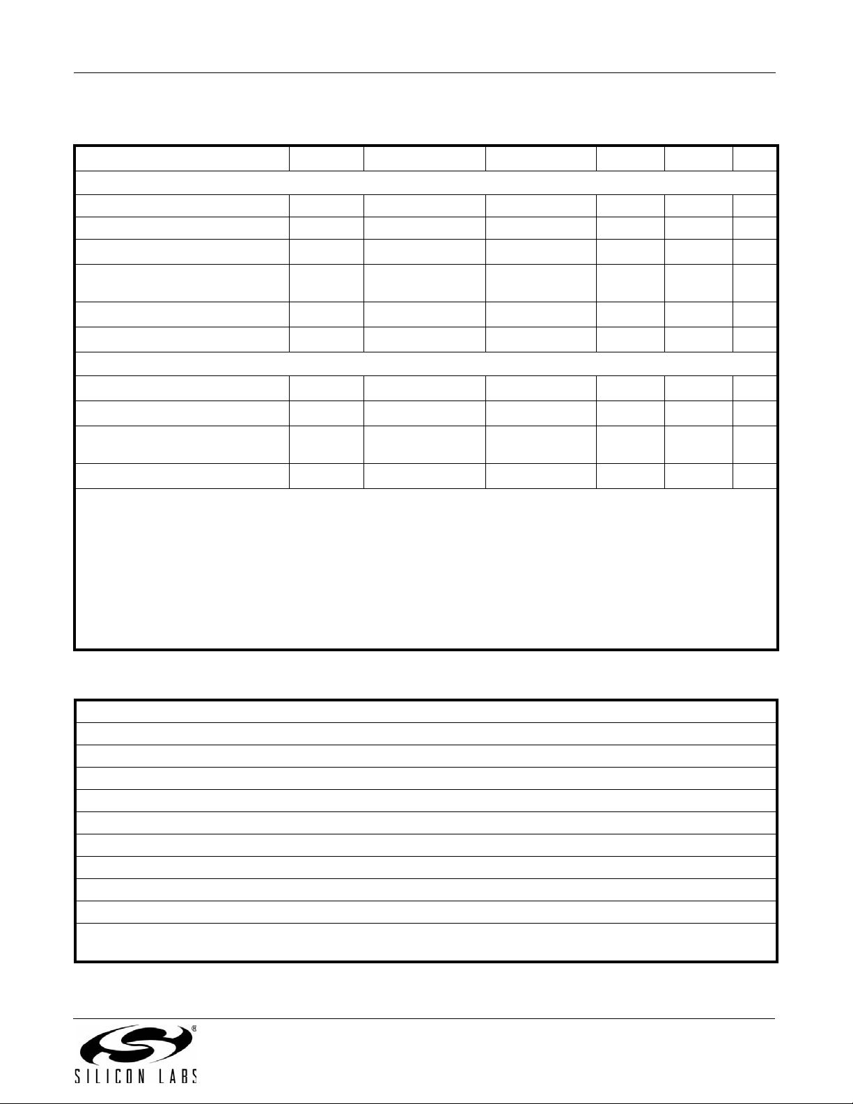
Table 6. Regulatory Information*
o
f
r N
basic insulation working voltage.
RMS
basic insulation working voltage.
RMS
rated devices which are production tested to 3.0 kV
RMS
Rev. 1.5 13
RMS
for 1 sec.
CSA
The Si84xx is certified under CSA Component Acceptance Notice 5A. For more details, see File 232873.
61010-1: Up to 300 V
60950-1: Up to 130 V
VDE
The Si84xx is certified according to IEC 60747-5-2. For more details, see File 5006301-4880-0001.
60747-5-2: Up to 560 V
UL
The Si84xx is certified under UL1577 component recognition program. For more details, see File E257455.
Rated up to 2500 V
*Note: Regulatory Certific ations apply to 2.5 kV
For more information, see "5. Ordering Guide" on page 25.
Not Recommended
reinforced insulation working voltage; up to 600 V
RMS
reinforced insulation working voltage; up to 600 V
RMS
for basic insulation working voltage.
peak
isolation voltage for basic insulati on.
RMS
Page 14
Si8410/20/21
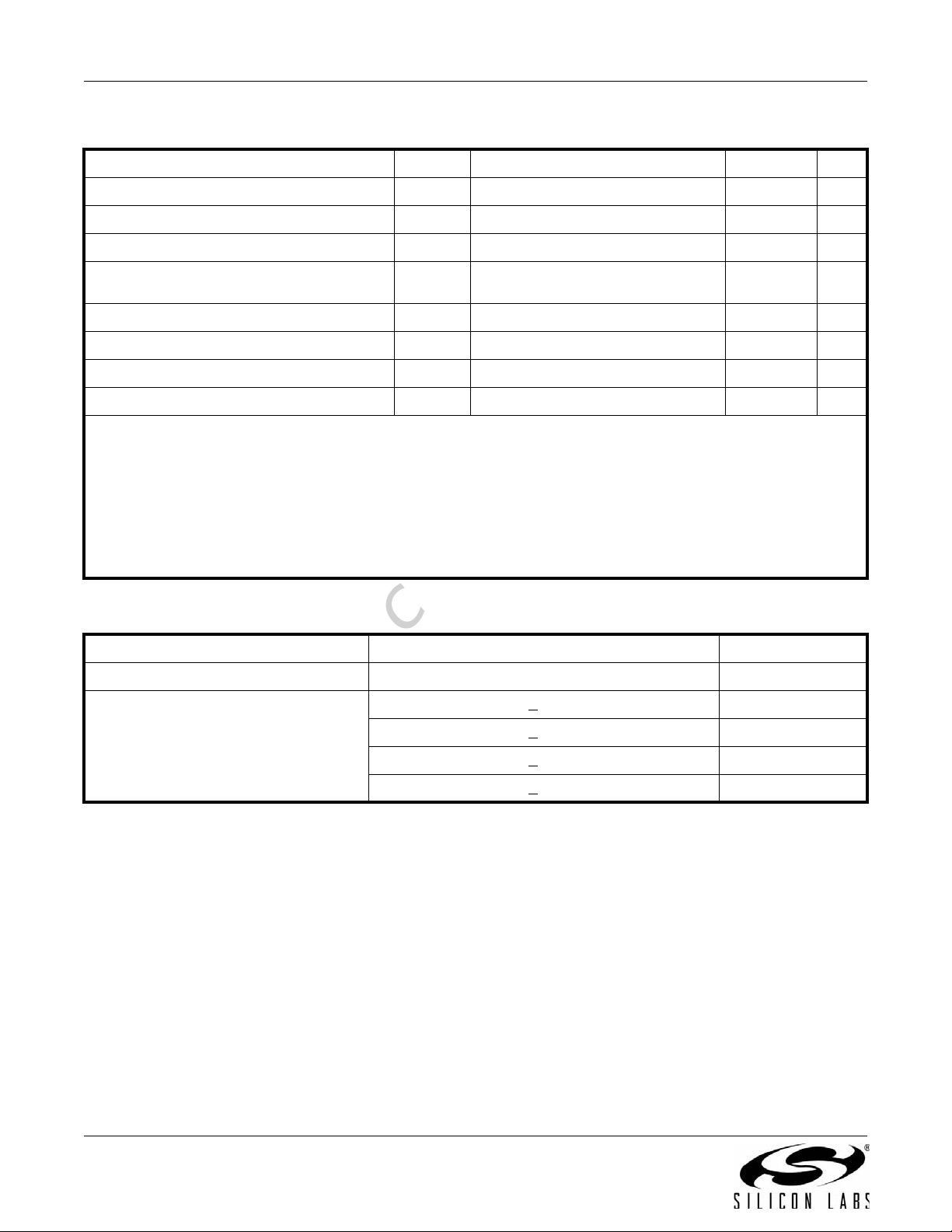
Table 7. Insulation and Safety-Related Specifications
Parameter Symbol Test Condition Value Unit
Nominal Air Gap (Clearance)
Nominal External Tracking (Creepage)
Minimum Internal Gap (Internal Clearance) 0.008 mm
1
1
L(IO1) 4.9 mm
L(IO2) 4.01 mm
Tracking Resistance
(Proof Tracking Index)
Erosion Depth
Resistance (Input-Output)
Capacitance (Input-Output)
Input Capacitance
Notes:
1. The values in this table correspond to the nominal creepage and clearance values as detailed in "6. Package Outline:
8-Pin Narrow Body SOIC" on page 26. VDE certifies the clearance and creepage limits as 4.7 mm minimum for the NB
SOIC-8 package. UL does not impose a clearance and creepage minimum for component level certifications. CSA
certifies the clearance and creepage limits as 3.9 mm minimum for the NB SOIC-8 package.
2. To determine resistance and capacitance, the Si84xx is converted into a 2-terminal device. Pins 1–4 are shorted
together to form the first terminal and pins 5–8 are shorted together to form the second terminal. The parameters are
then measured between these two terminals.
3. Measured from input pin to ground.
3
2
2
PTI IEC60112 600 V
ED 0.040 mm
R
IO
C
IO
C
I
f=1MHz 1.0 pF
12
10
4.0 pF
s
n
g
si
e
Table 8. IEC 60664-1 (VDE 0844 Part 2) Ratings
D
Parameter Test Condition Specification
Basic Isolation Group Material Group I
Rated Mains Voltages <
e
Rated Mains Voltages <
Installation Classification
Rated Mains Voltages <
Rated Mains Voltages <
r N
w
150 V
300 V
400 V
600 V
RMS
RMS
RMS
RMS
I-IV
I-III
I-II
I-II
Not Recommended
o
f
RMS
14 Rev. 1.5
Page 15
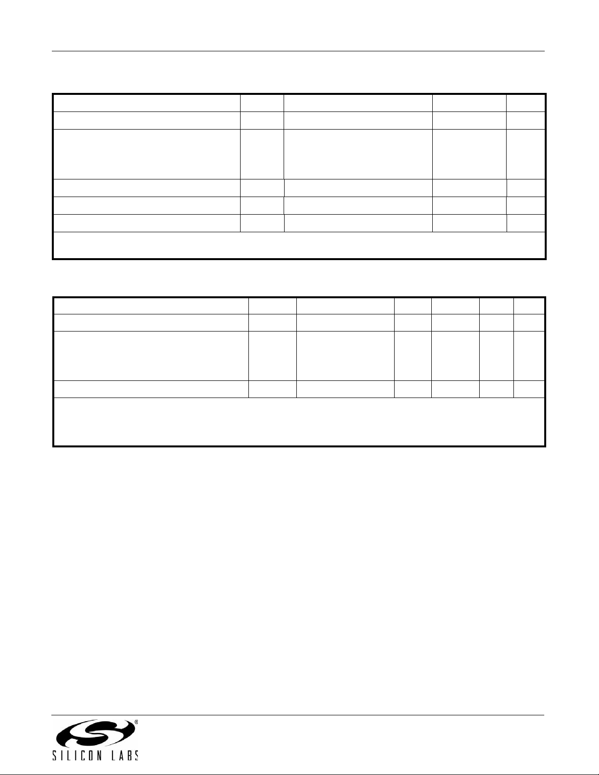
Table 9. IEC 60747-5-2 Insulation Characteristics for Si84xxxB*
Parameter Symbol Test Condition Characteristic Unit
Si8410/20/21
Maximum Working Insulation Voltage
Input to Output Test Voltage
Transient Overvoltage
Pollution Degree (DIN VDE 0110, Table 1)
Insulation Resistance at T
*Note: Maintenance of the safety data is ensured by protective circuits. The Si84xx provides a climate classification of
40/125/21.
Table 10. IEC Safety Limiting Values
Parameter Symbol Test Condition Min Typ Max Unit
Case Temperature T
Safety input, output, or supply current I
Device Power Dissipation
Notes:
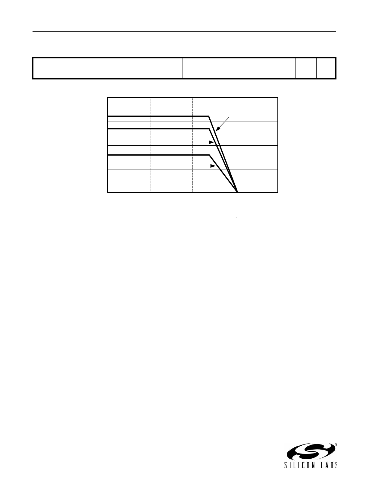
1. Maximum value allowed in the event of a failure; also see the thermal derating curve in Figure 2.
2. The Si841x/2x is tested with VDD1 = VDD2 = 5.5 V , TJ = 150 °C, CL = 15 pF, input a 150 Mbps 50% duty cycle square
wave.
, VIO=500V
S
2
V
IORM
Method b1
V
PR
V
IOTM
R
S
1
(V
Production Test, t
x 1.875 = VPR, 100%
IORM
Partial Discharge < 5 pC)
t = 60 sec 4000 V peak
=1 sec,
m
n
S
= 140 °C/W,
JA
V
=5.5V,
S
P
D
I
T
=150°C,
J
T
=25°C
A
D
e
—
g
si
——160mA
——150mW
w
560 V peak
1050
2
9
>10
s
—
150 °C
e
V peak
Not Recommended
r N
o
f
Rev. 1.5 15
Page 16
Si8410/20/21
0 20015010050
400
200
100
0
Case Temperature (ºC)
Safety-Limiting Values (mA)
320
300
V
DD1
, V
DD2
= 2.70 V
V
DD1
, V
DD2
= 3.3 V
V
DD1
, V
DD2
= 5.5 V
270
160
Table 11. Thermal Characteristics
Parameter Symbol Test Condition Min Typ Max Unit
IC Junction-to-Air Thermal Resistance
JA
—140—°C/W
s
n
g
Figure 2. (NB SOIC-8) Thermal Derating Curve, Dependence of Safety Limiting Values
with Case Temperature per DIN EN 60747-5-2
si
e
D
w
e
r N
Not Recommended
o
f
16 Rev. 1.5
Page 17
Si8410/20/21
RF
OSCILLATOR
MODULATOR DEMODULATOR
A B
Semiconductor-
Based Isolation
Barrier
Transmitter Receiver
Input Signal
Output Signal
Modulation Signal
2. Functional Description
2.1. Theory of Operation
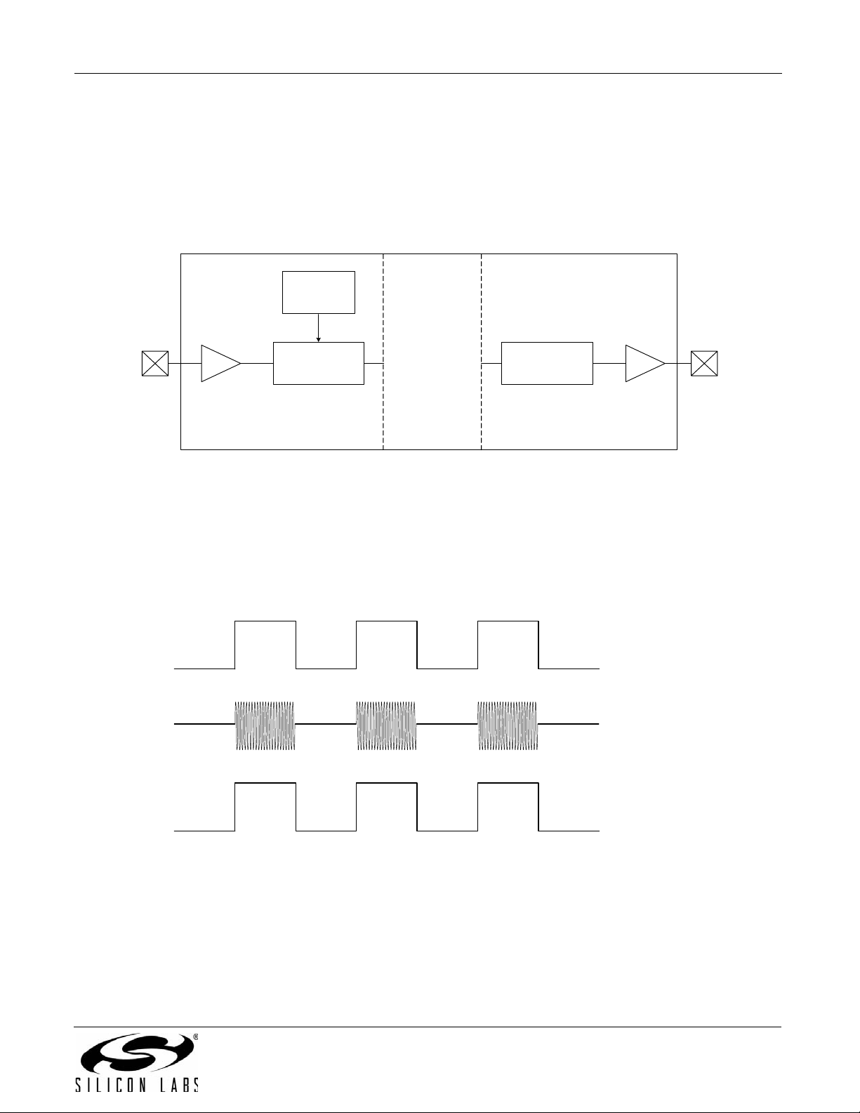
The operation of an Si84xx channel is analogous to that of an opto coupler, except an RF carrier is modulated
instead of light. This simple architecture provides a robust isolated data path and requires no special
considerations or initialization at start-up. A simplified block diagram for a single Si84xx channel is shown in
Figure 3.
s
n
Figure 3. Simplified Channel Diagram
A channel consists of an RF Transmitter and RF Receiver separated by a semiconductor-based isolation barrier.
Referring to the Transmitter, input A modulates the carrier provided by an RF oscillator using on/off keying. The
Receiver contains a demodulator that decodes the input state according to its RF energy content and applies the
result to output B via the output driver. This RF on/off keying scheme is superior to pulse code schemes as it
provides best-in-class noise immunity, low power consumption, and better immunity to magnetic fields. See
Figure 4 for more details.
e
D
g
si
w
e
r N
Not Recommended
o
f
Figure 4. Modulation Scheme
Rev. 1.5 17
Page 18
Si8410/20/21
2.2. Eye Diagram
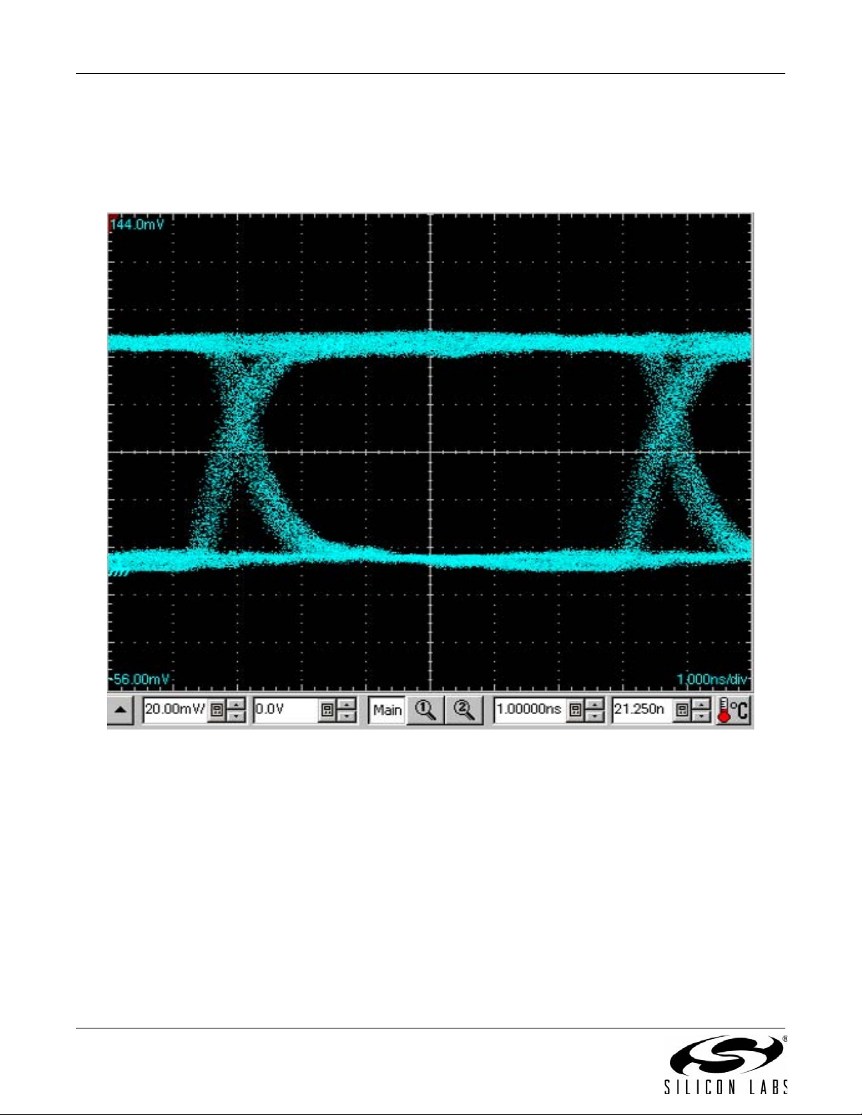
Figure 5 illustrates an eye-diagram taken on an Si8410. For the data source, the test used an Anritsu (MP1763C)
Pulse Pattern Generator set to 1000 ns/div. The output of the generator's clock and data from an Si8410 were
captured on an oscilloscope. The results illustrate that data integrity was maintained even at the high data rate of
150 Mbps. The results also show that 2 ns pulse width distortion and 250 ps peak jitter were exhibited.
s
n
g
si
e
D
w
e
r N
Not Recommended
o
Figure 5. Eye Diagram
f
18 Rev. 1.5
Page 19
2.3. Device Operation
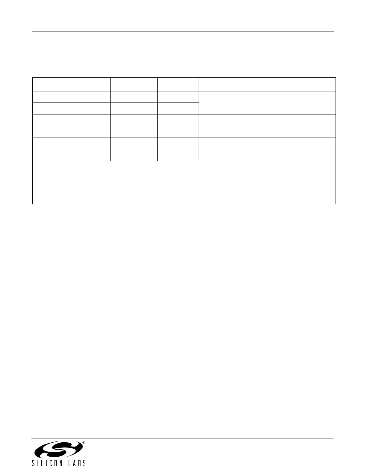
Device behavior during start-up, normal operation, and shutdown is shown in Table 12.
Table 12. Si84xx Logic Operation Table
Si8410/20/21
VI Input
Notes:
1,4
VDDI State
HP P H
LP P L
5
X
5
X
1. VDDI and VDDO are the input and output power supplies. V
2. Powered (P) state is defined as 2.70 V < VDD < 5.5 V.
3. Unpowered (UP) state is defined as VDD = 0 V.
4. X = not applicable; H = Logic High; L = Logic Low.
5. Note that an I/O can power the die for a given side through an internal diode if its source has adequate current.
1,2,3
VDDO State
UP P L
P UP Undetermined
1,2,3
VO Output
1,4
Normal operation.
Upon transition of VDDI from unpowered to powered, V
than 1 µs.
Upon transition of VDDO from unpowered to powered, V
1µs.
and VO are the respective input and output terminals.
I
returns to the same state as VI in less
O
returns to the same state as VI within
O
Comments
s
n
g
si
e
D
w
e
r N
Not Recommended
o
f
Rev. 1.5 19
Page 20
Si8410/20/21
VDD1 VDD2
GND1 GND2
50 – 300 50 – 300
Input/OutputInput/Output
C2 C3
1
F 1 F
R1 (50 – 100 )
V Source 1
A1
B1
50 – 300
50 – 300
Ax
Bx
C1
R2 (50 – 100 )
V Source 2
C4
0.1
F 0.1 F
2.4. Layout Recommendations
To ensure safety in the end user application, high voltage circuits (i.e., circuits with >30 VAC) must be physically
separated from the safety extra-low voltage circuits (SELV is a circuit with <30 V
(creepage/clearance). If a c omponent, such as a digital isolator, straddles this isolation barrier, it must meet those
creepage/clearance requirements and also provide a sufficiently large high-voltage breakdown protection rating
(commonly referred to as working voltage protection). Table 6 on page 13 and Table 7 on page 14 detail the
working voltage and creepage/clearance capabilities of the Si84xx. These tables also detail the component
standards (UL1577, IEC60747, CSA 5A), which are readily accepted by certification bodies to provide proof for
end-system specifications requirements. Refer to the end-system specification (61010-1, 60950-1, etc.)
requirements before starting any design that uses a digital isolator.
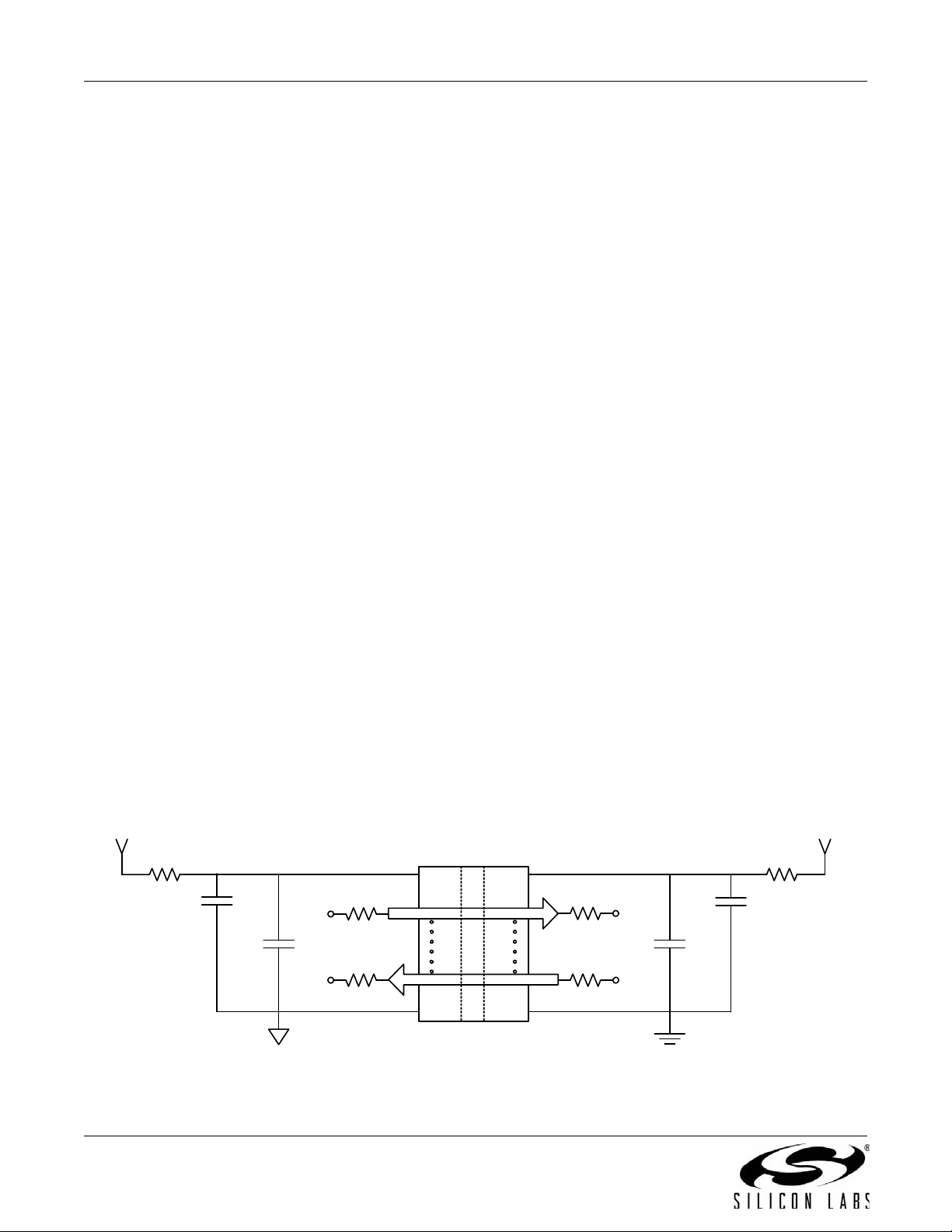
The following sections detail the recommended bypass and decoupling components necessary to ensure robust
overall performance and reliability for systems using the Si84xx digital isolators.
2.4.1. Supply Bypass
Digital integrated circuit components typically require 0.1 µF (100 nF) bypass capacitors when used in electrically
quiet environments. However, digital isolators are commonly used in hazardous environments with excessively
noisy power supplies. To counteract these harsh conditions, it is recommended that an additional 1 µF bypass
capacitor be added between VDD and GND on both sides of the package. The capacitors should be placed as
close as possible to the package to minimize stray inductance. If the system is excessively noisy, it is
recommended that the designer add 50 to 100 resistors in series with the VDD supply voltage source and 50 to
300 resistors in series with the digital inputs/outputs (see Figure 6). For more details, see "3. Errata and Design
Migration Guidelines" on page 23.
All components upstream or downstream of the isolator should be properly decoupled as well. If these components
are not properly decoupled, their supply noise can couple to the isolator inputs and outputs, potentially causing
damage if spikes exceed the maximum ratings of the isolator (6 V). In this case, the 50 to 300 resistors protect
the isolator's inputs/outputs (note that permanent device damage may occur if the absolute maximum ratings are
exceeded). Functional operation should be restricted to the conditions specified in Table 1, “Recommended
Operating Conditions,” on page 4.
2.4.2. Pin Connections
No connect pins are not internally connected. They can be left floating, tied to
2.4.3. Output Pin Termination
The nominal output impedance of an isolator driver channel is approximately 85 , ±40%, which is a combination
of the value of the on-chip series termination resistor and cha nnel resist ance of the output driver FET. When driving
loads where transmission line effects will be a factor , output pins should be appropriately terminated with controlled
impedance PCB traces. The series termination resistor values should be scaled appropriately while keeping in
mind the recommendations described in “2.4.1. Supply Bypass” above.
Not Recommended
r N
e
w
e
D
g
si
V
, or tied to GND.
DD
) by a certain distance
AC
s
n
o
f
Figure 6. Recommended Bypass Components for the Si84xx Digital Isolator Family
20 Rev. 1.5
Page 21
Si8410/20/21
0
5
10
15
20
25
30
0 10 20 30 40 50 60 70 80 90 100 110 120 130 140 150
Data Rate (Mbps)
Current (mA)
5V
3.3V
2.70V
0
5
10
15
20
25
30
0 10 20 30 40 50 60 70 80 90 100 110 120 130 140 150
Data Rate (Mb p s)
Curren t (mA)
5V
3.3V
2.70V
0
5
10
15
20
25
30
0 10 20 30 40 50 60 70 80 90 100 110 120 130 140 150
Data Rate (Mb p s)
Curren t (mA)
5V
3.3V
2.70V
0
5
10
15
20
25
30
0 102030405060708090100110120130140150
Data Ra te (Mb p s)
Current (mA)
5V
3.3V
2.70V
0
5
10
15
20
25
30
0 10 20 30 40 50 60 70 80 90 100 110 120 130 140 150
Data Rate (Mb p s)
Curren t (mA)
5V
2.70V
3.3V
5
6
7
8
9
10
-40 -20 0 20 40 60 80 100 120
Temperature (Degrees C)
Delay (ns)
Risi ng Edge
Falli ng Edge
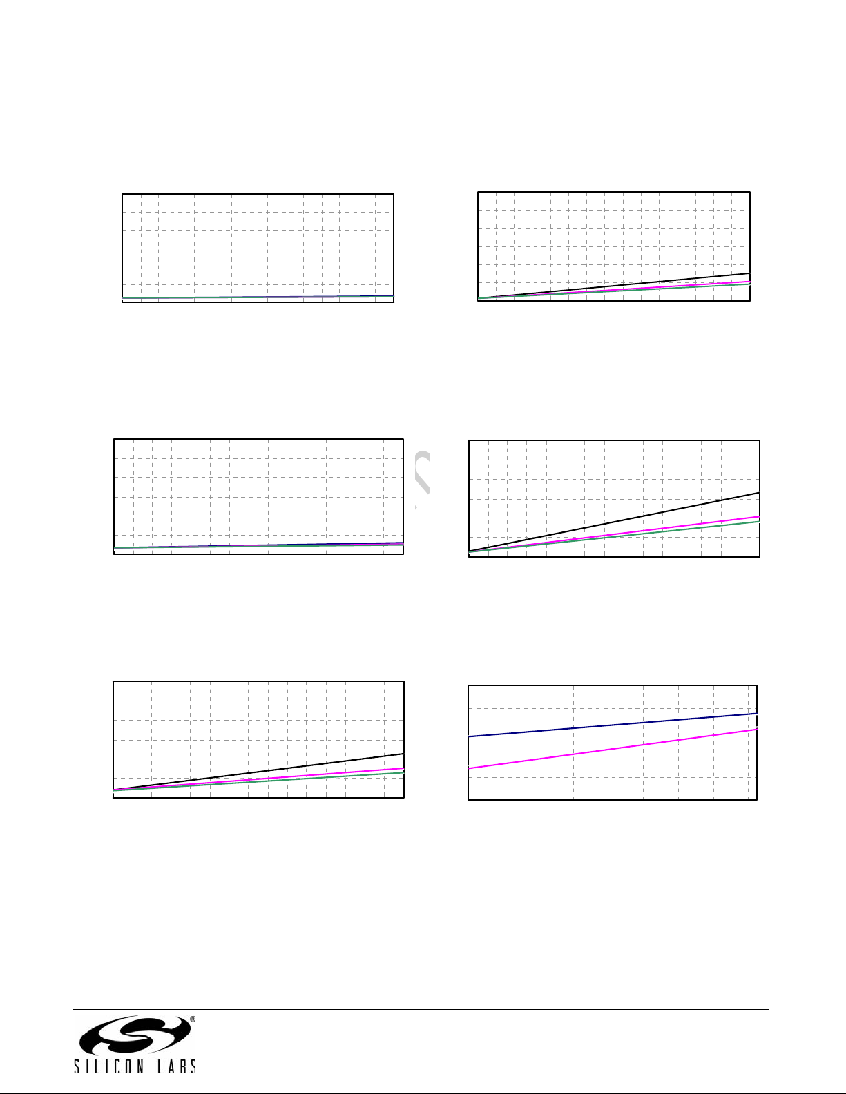
2.5. Typical Performance Characteristics
The typical performance characteristics depicted in th e follo wing diagra ms ar e for info rma tion p urpose s only. Refer
to Tables 3, 4, and 5 for actual specification limits.
Figure 7. Si8410 Typical V
vs. Data Rate 5, 3.3, and 2.70 V Operation
Figure 8. Si8420 Typical V
vs. Data Rate 5, 3.3, and 2.70 V Operation
Supply Current
DD1
Supply Current
DD1
r N
Not Recommended
o
f
Figure 10. Si8410 Typical V
vs. Data Rate 5, 3.3, and 2.70 V Operation
si
e
D
w
Figure 11. Si8420 Typical V
e
vs. Data Rate 5, 3.3, and 2.70 V Operation
DD2
(15 pF Load)
s
n
g
DD2
(15 pF Load)
Supply Current
Supply Current
Figure 9. Si8421 Typical V
Current vs. Data Rate 5, 3.3, and 2.70 V
Operation (15 pF Load)
DD1
or V
DD2
Supply
Rev. 1.5 21
Figure 12. Propagation Delay
vs. Temperature
Page 22
Si8410/20/21
s
n
g
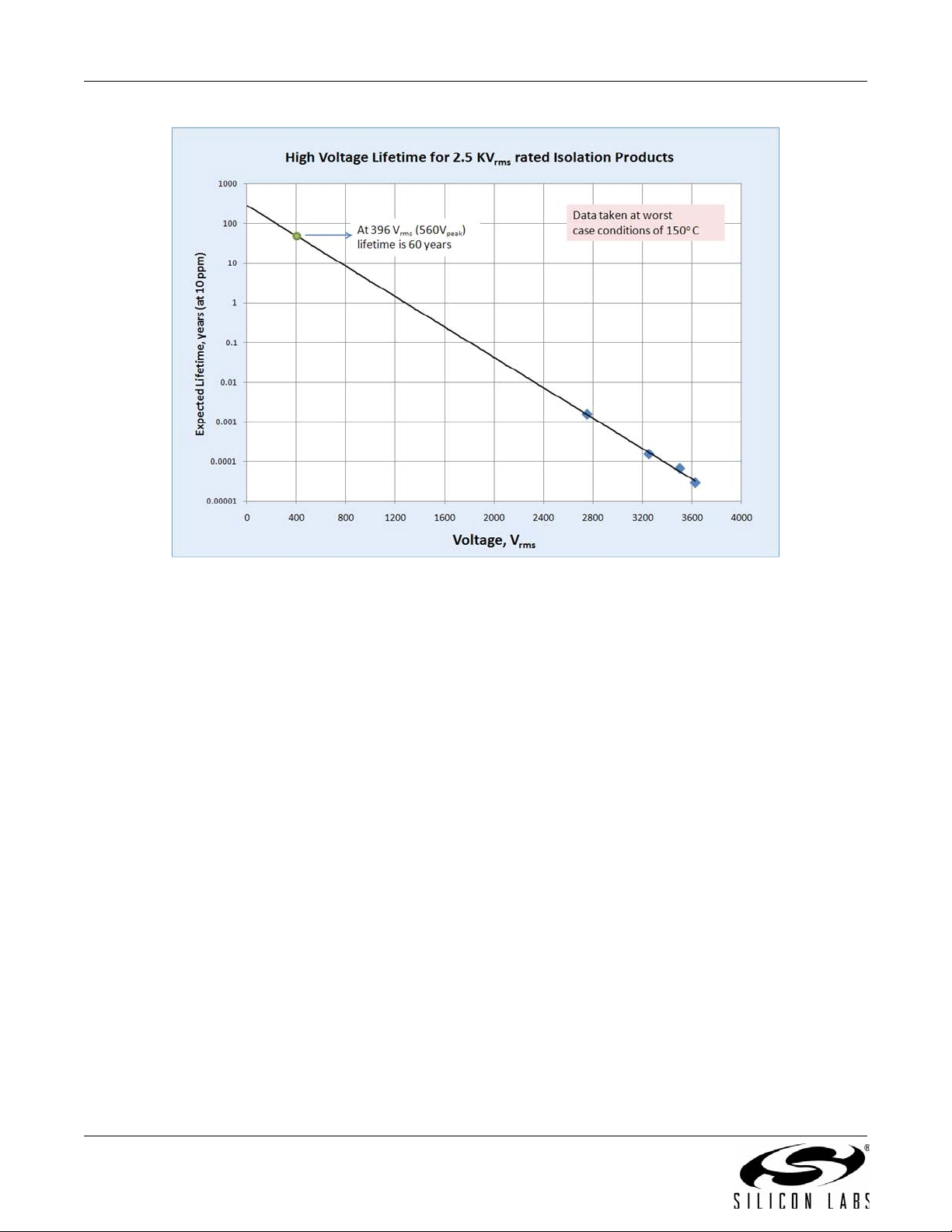
Figure 13. Si84xx Time-Dependent Dielectric Breakdown
si
e
D
w
e
r N
Not Recommended
o
f
22 Rev. 1.5
Page 23
Si8410/20/21
3. Errata and Design Migration Guidelines
The following errata apply to Revision C devices only. See "5. Ordering Guide" on page 25 for more details. No
errata exist for Revision D devices.
3.1. Power Supply Bypass Capacitors (Revision C and Revision D)
When using the Si84xx isolators with power supplies > 4.5 V , sufficient VDD bypass capacitors must be present on
both the VDD1 and VDD2 pins to ensure the VDD rise time is less than 0.5 V/µs (which is > 9 µs for a >
supply). Although rise time is power supply dependent, >
(VDD1, VDD2) of the isolator device.
3.1.1. Resolution
For recommendations on resolving this issue, see "2.4.1. Supply Bypass" on pa ge 20. Additionally, refer to "5.
Ordering Guide" on page 25 for current ordering information.
3.2. Latch Up Immunity (Revision C Only)
Si84xx latch up immunity generally exceeds ± 200 mA per pin. Exceptions: Certain pins provide < 100 mA of latchup immunity. To increase latch-up immunity on these pins, 100 of equivalent resistance must be included in
series with all of the pins listed in Table 13. The 100 equivalent resistance can be comprised of the source
driver's output resistance and a series termination resistor. The Si8410 is not affected by the latch up immunity
issue described above.
3.2.1. Resolution
This issue has been corrected with Revision D of the device. Refer to “5. Ordering Guide” for current ordering
information.
1 µF capacitors are required on both power supply pins
s
n
g
4.5 V
si
Table 13. Affected Ordering Part Numbers (Revision C Only)
Affected Ordering Part Numbers*
Device
Revision
e
Pin# Name Pin Type
D
SI8420SV-C-IS, SI8421SV-C- IS C
w
3 A2 Input or Output
7 B1 Output
*Note: SV = Speed Grade/Isolation Rating (AA, AB, BA, BB).
e
r N
Not Recommended
o
f
Rev. 1.5 23
Page 24
Si8410/20/21
I
s
o
l
a
t
i
o
n
VDD1
VDD2
A1
RF
XMITR
B1
RF
RCVR
GND1
GND2
Si8410 NB SOIC-8
VDD1/NC
GND2/NC
I
s
o
l
a
t
i
o
n
VDD1
VDD2
A1
B1
RF
XMITR
RF
RCVR
A2
B2
RF
XMITR
RF
RCVR
GND1
GND2
Si8420 NB SOIC-8
I
s
o
l
a
t
i
o
n
VDD1
VDD2
A1
B1
RF
XMITR
RF
RCVR
A2
B2
RF
XMITR
RF
RCVR
GND1
GND2
Si8421 NB SOIC-8
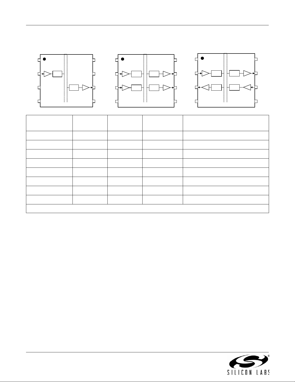
4. Pin Descriptions
Name SOIC-8 Pin#
Si8410
V
/NC* 1,3 1 Supply Side 1 power supply.
DD1
GND1 4 4 Ground Side 1 ground.
A1 2 2 Digital I/O Side 1 digital input or output.
A2 NA 3 Digital I/O Side 1 digital input or output.
B1 6 7 Digital I/O Side 2 digital input or output.
B2 NA 6 Digital I/O Side 2 digital input or output.
V
DD2
GND2/NC* 5,7 5 Ground Side 2 ground.
*Note: No Connect. These pins are not internally connected. They can be left floating, tied to VDD or tied to GND.
8 8 Supply Side 2 power supply.
SOIC-8 Pin#
Si8420/21
Type Description
s
n
g
si
e
D
w
e
r N
Not Recommended
o
f
24 Rev. 1.5
Page 25
Si8410/20/21
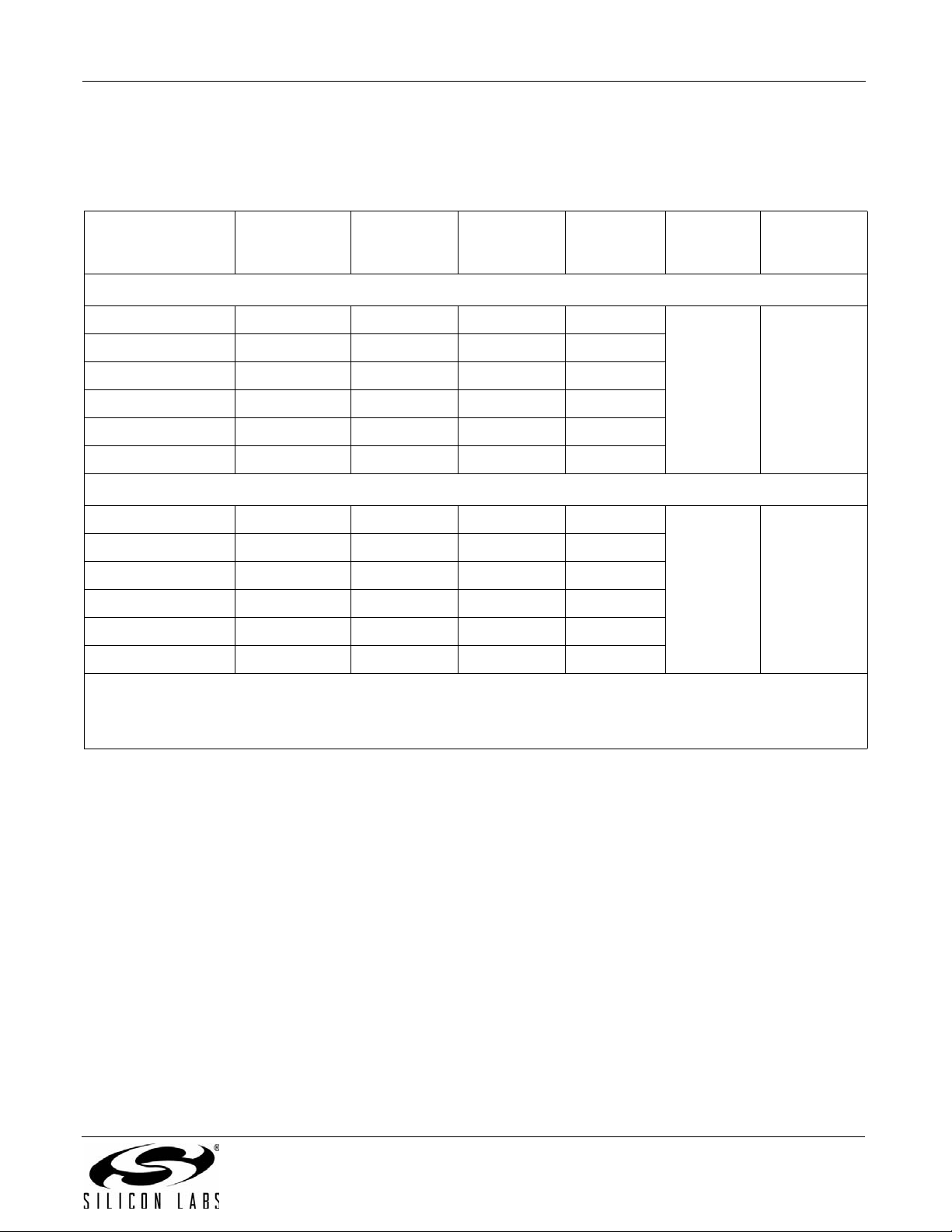
5. Ordering Guide
These devices are not recommended for new designs. Please see the Si861x datasheet for replacement options.
Table 14. Ordering Guide for Valid OPNs
Ordering Part
Number
(OPN)
Revision D Devices
Si8410AB-D-IS
Si8410BB-D-IS
Si8420AB-D-IS
Si8420BB-D-IS
Si8421AB-D-IS
Si8421BB-D-IS
Revision C Devices
Si8410AB-C-IS
Si8410BB-C-IS
Si8420AB-C-IS
Si8420BB-C-IS
Si8421AB-C-IS
Si8421BB-C-IS
Notes:
1. All packages are RoHS-compliant. Moisture sensitivity level is MSL2A with peak reflow temperature of 260 °C
according to the JEDEC industry standard classifications and peak solder temperature.
2. Revision C and Revision D devices are supported for existing designs.
Alternative
Part Number
(APN)
2
Si8610AB-B-IS
Si8610BB-B-IS
Si8620AB-B-IS
Si8620BB-B-IS
Si8621AB-B-IS
Si8621BB-B-IS
2
Si8610AB-B-IS
Si8610BB-B-IS
Si8620AB-B-IS
Si8620BB-B-IS
Si8621AB-B-IS
Si8621BB-B-IS
Number of
Inputs VDD1
Side
101
10150
201
20150
111
11150
101
10150
201
20150
111
11150
Number of
Inputs VDD2
Side
D
Maximum
Data Rate
e
w
e
1
Isolation
Rating
(Mbps)
2.5 kVrms NB SOIC-8
s
n
g
si
2.5 kVrms NB SOIC-8
Package
Type
Not Recommended
r N
o
f
Rev. 1.5 25
Page 26
Si8410/20/21
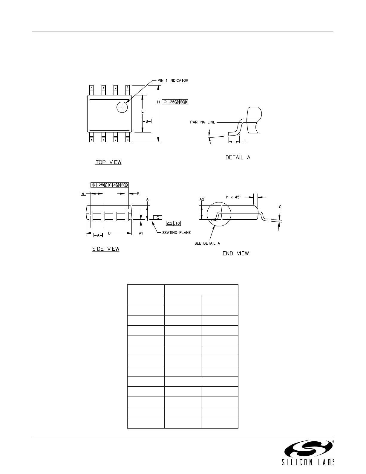
6. Package Outline: 8-Pin Narrow Body SOIC
Figure 14 illustrates the package details for the Si841x. Table 15 lists the values for the dimensions shown in the
illustration.
s
n
g
si
e
D
Figure 14. 8-pin Small Outline Integrated Circuit (SOIC) Package
Table 15. Package Diagram Dimensions
Symbol
r N
Not Recommended
A 1.35 1.75
o
A1 0.10 0.25
f
A2 1.40 REF 1.55 REF
B 0.33 0.51
C 0.19 0.25
D 4.80 5.00
E 3.80 4.00
e 1.27 BSC
H 5.80 6.20
w
e
Millimeters
Min Max
h 0.25 0.50
L 0.40 1.27
26 Rev. 1.5
0 8
Page 27
Si8410/20/21
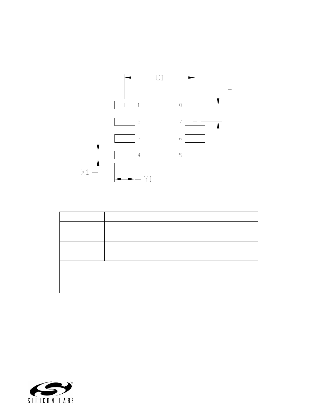
7. Land Pattern: 8-Pin Narrow Body SOIC
Figure 15 illustrates the recommended land pattern details for the Si841x in an 8-pin narrow-body SOIC. Table 16
lists the values for the dimensions shown in the illustration.
s
n
g
si
Figure 15. PCB Land Pattern: 8-Pin Narrow Body SOIC
e
Table 16. PCM Land Pattern Dimensions (8-Pin Narrow Body SOIC)
D
Dimension Feature (mm)
C1 Pad Column Spacing 5.40
E Pad Row Pitch 1.27
X1 Pad Width 0.60
Y1 Pad Length 1.55
Notes:
Not Recommended
1. This Land Pattern Design is based on IPC-7351 pattern SOIC127P600X173-8N for
Density Level B (Median Land Protrusion).
2. All feature sizes shown are at Maximum Material Condition (MMC) and a card
fabrication tolerance of 0.05 mm is assumed.
r N
o
f
e
w
Rev. 1.5 27
Page 28
Si8410/20/21
Si84XYSV
AIXX
e3
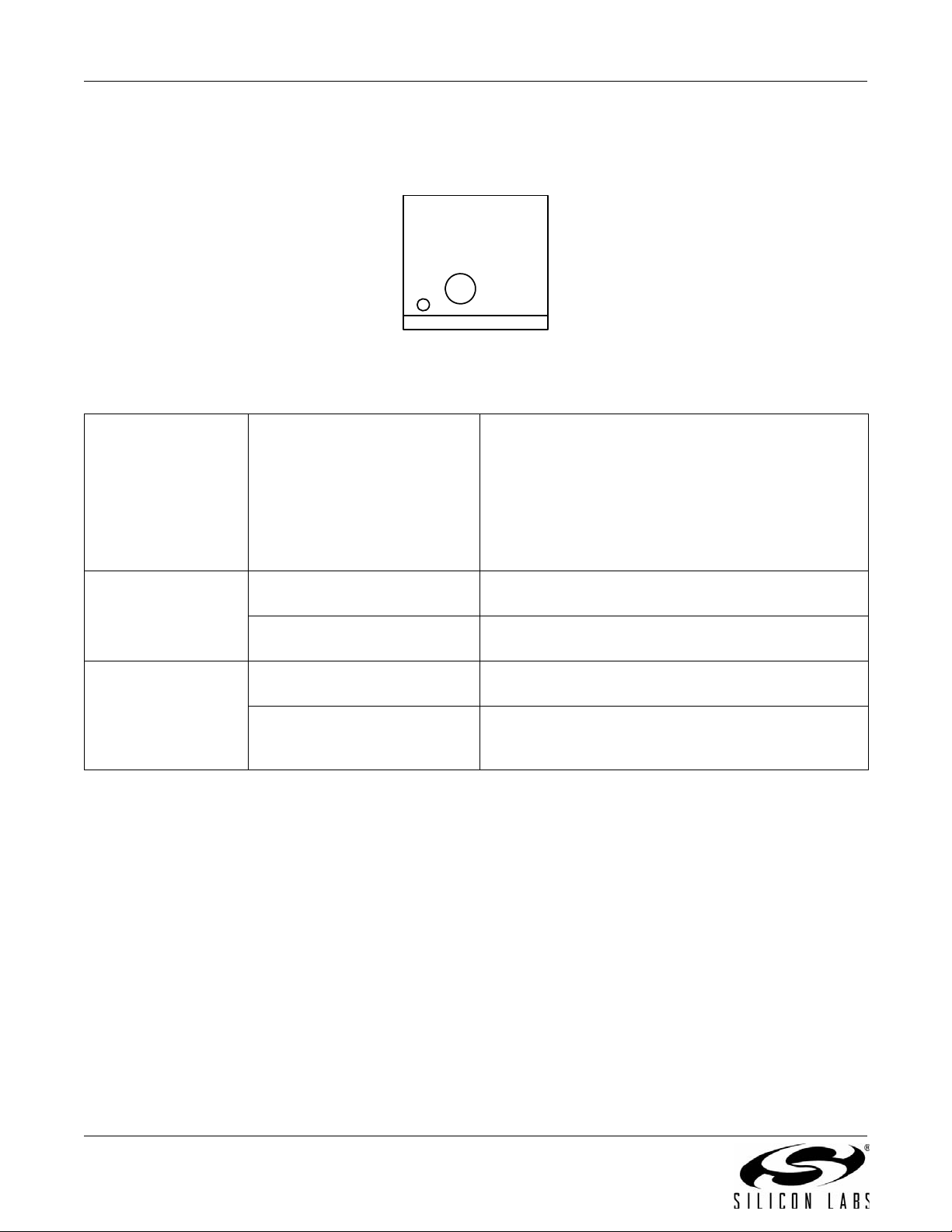
8. Top Marking: 8-Pin Narrow Body SOIC
8.1. 8-Pin Narrow Body SOIC Top Marking
YYWWRF
8.2. Top Marking Explanation
Table 17. Top Marking Explanations
Line 1 Marking: Base Part Number
Ordering Options
(See Ordering Guide for more
information).
Line 2 Marking: YY = Year
WW = Workweek
R = Product (OPN) Revision
F=Wafer Fab
Line 3 Marking: Circle = 1.1 mm Diameter
Left-Justified
A = Assembly Site
I = Internal Code
XX = Serial Lot Number
r N
Not Recommended
o
f
Si84 = Isolator product series
XY = Channel Configuration
X = # of data channels (2, 1)
Y = # of reverse channels (1, 0)
S = Speed Grade
A = 1 Mbps; B = 150 Mbps
V = Insulation rating
A=1kV; B=2.5kV
Assigned by Assembly Contractor. Corresponds to the
year and workweek of the mold date.
e
g
si
s
n
D
“e3” Pb-Free Symbol
w
First Two Characters of the Manufacturing Code
e
Last Four Characters of the Manufacturing Code
28 Rev. 1.5
Page 29

Si8410/20/21
DOCUMENT CHANGE LIST
Revision 0.1 1 to Revision 0.21
Rev 0.21 is the first revision of this document that
applies to the new series of ultra low power isolators
featuring pinout and functional compatibility with
previous isolator products.
Updated “1. Electrical Specifications”.
Updated “5. O r de rin g Guid e”.
Added “8. Top Marking: 8-Pin Narrow Body SOIC”.
Revision 0.21 to Revision 0.22
Updated all specs to reflect latest silicon.
Revision 0.22 to Revision 0.23
Updated all specs to reflect latest silicon.
Added "3. Errata and Design Migration Guidelines"
on page 23.
Revision 0.23 to Revision 1.0
Updated document to reflect availability of Revision
D silicon.
Updated Tables 3,4, and 5.
Updated all supply currents and channel-channel skew.
Updated Table 2.
Updated absolute maximum supply voltage.
Updated Table 7.
Updated clearance and creepage dimensions.
Updated "3. Errata and Design Migration Guidelines"
on page 23.
Updated "5. Ordering Guide" on page 25.
e
Revision 1.2 to Revision 1.3
Updated " Features" on page 1.
Moved Tables 1 and 2 to page 4.
Updated Tables 6, 7, 8, and 9.
Updated Table 12 footnotes.
Added Figure 13, “Si84xx Time-Dependent
Dielectric Breakdown,” on page 22.
Revision 1.3 to Revision 1.4
Updated "2.4.1. Supply Bypass" on page 20.
Added Figure 6, “Recommended Bypass
Components for the Si84xx Digital Isolator Family,”
on page 20.
Updated "3.1. Power Supply Bypass Capacitors
(Revision C and Revision D)" on page 23.
Revision 1.4 to Revision 1.5
Updated "5. Ordering Guide" on page 25 to include
new title note and “ Alternative Part Number (APN)”
column.
s
n
g
si
e
D
w
Revision 1.0 to Revision 1.1
Updated Tables 3, 4, and 5.
Updated notes in tables to reflect output impedance of
85 .
Updated rise and fall time specifications.
Updated CMTI value.
Revision 1.1 to Revision 1.2
Updated document throughout to include MSL
improvements to MSL2A.
Updated "5. Ordering Guide" on page 25.
Updated Note 1 in ordering guide table to reflect
improvement and compliance to MSL2A moisture
sensitivity level.
Not Recommended
r N
o
f
Rev. 1.5 29
Page 30
Si8410/20/21
The information in this document is believed to be accurate in all respects at the time of publication but is subject to change without notice.
Silicon Laboratories assumes no responsibility for errors and omissions, and disclaims responsibility for any consequences resulting from
the use of information included herein. Additionally, Silicon Laboratories assumes no responsibility for the functioning of undescribed features or parameters. Silicon Laboratories reserves the right to make changes without further notice. Silicon Laboratories makes no warranty, representation or guarantee regarding the suitability of its products for any particular purpose, nor does Silicon Laboratories assume any
liability arising out of the application or use of any product or circuit, and specifically disclaims any and all liability, including without limitation
consequential or incidental damages. Silicon Laboratories products are not designed, intended, or authorized for use in applications intended to support or sustain life, or for any other application in which the failure of the Silicon Laboratories product could create a situation where
personal injury or death may occur. Should Buyer purchase or use Silicon Laboratories products for any such unintended or unauthorized
application, Buyer shall indemnify and hold Silicon Laboratories harmless against all claims and damages.
CONTACT INFORMATION
Silicon Laboratories Inc.
400 West Cesar Chavez
Austin, TX 78701
Tel: 1+(512) 416-8500
Fax: 1+(512) 416-9669
Toll Free: 1+(877) 444-3032
Please visit the Silicon Labs Technical Support web page:
https://www.silabs.com/support/pages/contacttechnicalsupport.aspx
and register to submit a technical support request.
s
n
g
si
e
D
w
e
r N
Not Recommended
Patent Notice
Silicon Labs invests in research and development to help our customers differentiate in the market with innovative low-power, small size, analogintensive mixed-signal solutions. Silicon Labs' extensive patent portfolio is a testament to our unique approach and world-class engineering team.
o
f
Silicon Laboratories and Silicon Labs are trademarks of Silicon Laboratories Inc.
Other products or brandnames mentioned herein are trademarks or registered trademarks of their respective holders.
30 Rev. 1.5
Page 31

Mouser Electronics
Authorized Distributor
Click to View Pricing, Inventory, Delivery & Lifecycle Information:
Silicon Laboratories:
SI8410BB-C-ISR SI8420BB-C-ISR SI8421BB-C-ISR
 Loading...