

Silicon Laboratories Si5397 User Manual

UG353: Si5397 Evaluation Board User's
Guide
The Si5397-EVB is used for evaluating the Si5397 Any-Frequency, Any-Output, JitterAttenuating Clock Any-Frequency, Any-Output, Jitter-Attenuating Clock Multiplier Revision A. The device grade and revision is distinguished by a white 1 inch x 0.187 inch
label installed in the lower left hand corner of the board. In the example below, the label
"SI5397A-A-EB" indicates the evaluation board has been assembled with an Si5397 device, Grade A,Revision A, installed. (For ordering purposes only, the terms “EB” and
“EVB” refer to the board and the kit, respectively. For the purpose of this document, the
terms are synonymous in context.)
KEY FEATURES
• Powered from USB port or external +5 V
power supply via screw terminals
•
Onboard 48 MHz XTAL allows standalone
or holdover mode of operation on the
Si5397
• CBPro™ GUI programmable VDD supply
allows device supply voltages of 3.3, 2.5,
or 1.8 V
• CBPro GUI programmable VDDO supplies
allow each of the eight outputs to have its
own supply voltage selectable from 3.3,
2.5, or 1.8 V
• CBPro GUI allows control and
measurement of voltage, current, and
power of VDD and all eight VDDO supplies
• Status LEDs for power supplies and
control/status signals of the Si5397
• SMA connectors for input clocks, output
clocks and optional external timing
reference clock
silabs.com | Building a more connected world. Rev. 0.1
UG353: Si5397 Evaluation Board User's Guide
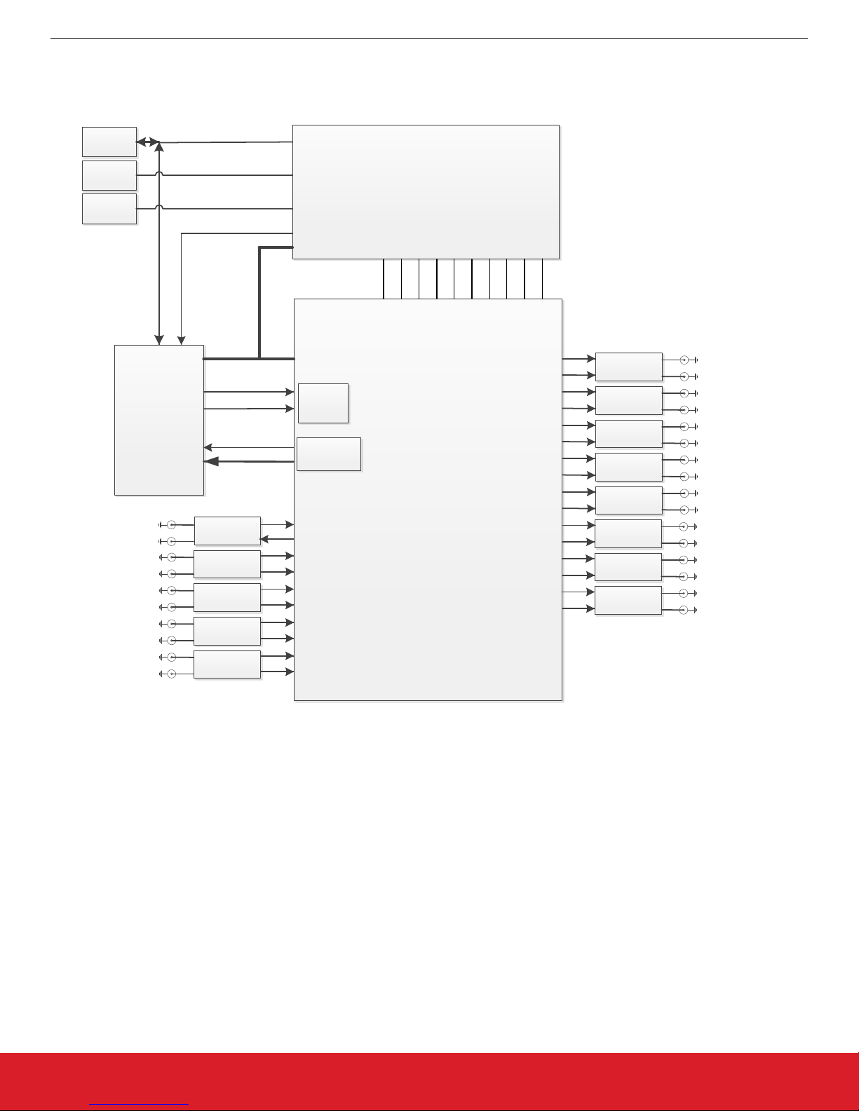
Functional Block Diagram
1. Functional Block Diagram
Below is a functional block diagram of the Si5397-A-EB. This evaluation board can be connected to a PC via the main USB connector
for programming, control, and monitoring. See 3. Quick Start or 10.3 Overview of ClockBuilderPro Applications for more information.
Main USB
Connector
Aux USB
Connector
Ext +5V
Connector
C8051F380
Peripherals
Optional External
XAXB Ref Input
Input Clock 0
Input Clock 1
Input Clock 2
Input Clock 3
MCU
+
{
{
{
{
{
Power only
Power only
XAXB
Crystal / Term
Input
Termination
Input
Termination
Input
Termination
Input
Termination
+5V_USB
+5V_Aux
+5V_Ext
VDDMCU
I2C/SPI Bus
I2C/SPI Bus
Control/
Status
INTR
Alarm_Status
XA
XB
CLKIN_0
CLKIN_0B
CLKIN_1
CLKIN_1B
CLKIN_2
CLKIN_2B
CLKIN_3
CLKIN_3B
Power Supply
VDDO_0
VDD_Core
VDD_3.3
VDDO_1
VDDO_2
VDDO_0
VDDO_1
VDD_3.3
VDD_Core
VDDO_2
Si5397
VDDO_3
VDDO_4
VDDO_3
VDDO_4
VDDO_5
VDDO_6
VDDO_7
VDDO_5
VDDO_6
VDDO_7
CLKOUT_0
CLKOUT_0B
CLKOUT_1
CLKOUT_1B
CLKOUT_2
CLKOUT_2B
CLKOUT_3
CLKOUT_3B
CLKOUT_4
CLKOUT_4B
CLKOUT_5
CLKOUT_5B
CLKOUT_6
CLKOUT_6B
CLKOUT_7
CLKOUT_7B
Output
Termination
Output
Termination
Output
Termination
Output
Termination
Output
Termination
Output
Termination
Output
Termination
Output
Termination
Output Clock 0
}
Output Clock 1
}
Output Clock 2
}
Output Clock 3
}
Output Clock 4
}
Output Clock 5
}
Output Clock 6
}
Output Clock 7
}
Figure 1.1. Si5397-A-EB Functional Block Diagram
silabs.com | Building a more connected world. Rev. 0.1 | 2

UG353: Si5397 Evaluation Board User's Guide
Si5397-A-EVB Support Documentation and ClockBuilderPro™ Software
2. Si5397-A-EVB Support Documentation and ClockBuilderPro™ Software
All Si5397-A-EVB schematics, BOMs, User’s Guides, and software can be found online at: http://www.silabs.com/products/clocksoscil-
lators/pages/si539x-evb.aspx.
silabs.com | Building a more connected world. Rev. 0.1 | 3

UG353: Si5397 Evaluation Board User's Guide
3. Quick Start
1. Install the ClockBuilderPro desktop software from http://www.silabs.com/CBPro.
2. Connect a USB cable from the Si5397-A-EB to the PC where the software was installed.
3. Leave the jumpers as installed from the factory, and launch the ClockBuilderPro software.
4. You can use ClockBuilderPro to create, download, and run a frequency plan on the Si5397-A-EB.
5. For the Si5397 data sheet, go to http://www.silabs.com/timing.
Quick Start
silabs.com | Building a more connected world. Rev. 0.1 | 4

4. Jumper Defaults
UG353: Si5397 Evaluation Board User's Guide
Jumper Defaults
1
I = Installed
Location Type
Table 4.1. Si5397-EB Jumper Defaults
I= Installed
0 = Open
Location Type
JP1 2-pin I JP23 2-pin O
JP2 2-pin O JP24 2-pin O
JP3 2-pin I JP25 2-pin O
JP4 2-pin I JP26 2-pin O
JP5 2-pin O JP27 2-pin O
JP6 2-pin O JP28 2-pin O
JP7 2-pin I JP29 2-pin O
JP8 2-pin O JP30 2-pin O
JP9 2-pin O JP31 2-pin O
JP10 2-pin I JP32 2-pin O
JP13 2-pin O JP33 2-pin O
JP14 2-pin I JP34 2-pin O
JP15 3-pin all open JP35 2-pin O
0 = Open
JP16 3-pin 1 to 2 JP36 2-pin O
JP17 2-pin O JP38 3-pin All Open
JP18 2-pin O JP39 2-pin O
JP19 2-pin O JP40 2-pin I
JP20 2-pin O JP41 2-pin I
JP21 2-pin O J36 5 x 2 Hdr All 5 installed
JP22 2-pin O
Note:
1.
Refer to the Si5397-A-EB schematics for the functionality associated with each jumper.
silabs.com | Building a more connected world. Rev. 0.1 | 5

5. Status LEDs
Location Silkscreen Color Status Function Indication
D27 5VUSBMAIN Blue Main USB +5 V present
D22 3P3V Blue DUT +3.3 V is present
D26 VDD DUT Blue DUT VDD voltage present
D25 INTR Red MCU INTR (Interrupt) active
D21 READY Green MCU Ready
D24 BUSY Green MCU Busy
D2 LOS_XAXB_B Blue Loss of Signal at XAXB input
D5 LOL_AB Blue Lossof Lock - DSPLL A
D6 LOL_BB Blue Lossof Lock - DSPLL B
D8 LOL_CB Blue Lossof Lock - DSPLL C
D11 INTRB Blue Si5397 Interrupt Active
D12 LOL_DB Blue Loss of Lock _ DSPLL D
UG353: Si5397 Evaluation Board User's Guide
Status LEDs
D27, D22, and D26 are illuminated when USB +5 V, Si5397 +3.3 V, and Si5397 Vcore supply voltages, respectively, are present. D25,
D21,
and D24 are status LEDs showing onboard MCU activity. D2 indicates loss of signal at XAXB input (either crystal osc or external
reference). D5, D6, D8, D12 indicate loss of lock for one of four internal DSPLLs (A–D). D11 indicates the Si5397 interrupt output is
active (as configured by Si5397 register programming). LED locations are highlighted below with LED function name indicated on board
silkscreen.
silabs.com | Building a more connected world. Rev. 0.1 | 6
Figure 5.1. Status LEDs
UG353: Si5397 Evaluation Board User's Guide
External Reference Input (XA/XB)
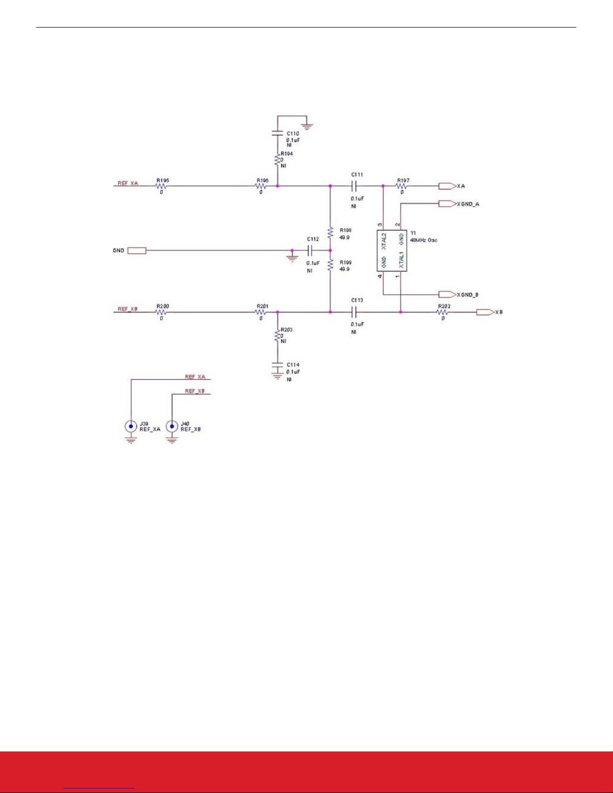
6. External Reference Input (XA/XB)
An external timing reference (48 MHz XTAL) is used in combination with the internal oscillator to produce an ultra-low jitter reference
clock for the DSPLL and for providing a stable reference for the free-run and holdover modes.The Si5397-A-EB can also accommodate
an external reference clock instead of a crystal.To evaluate the device with an external REFCLK, C111 and C113 must be populated
and XTAL Y1 removed (see figure below). The REFCLK can then be applied to SMA connectors J39 and J40.
Figure 6.1. External Reference Input Circuit
silabs.com | Building a more connected world. Rev. 0.1 | 7
UG353: Si5397 Evaluation Board User's Guide
Clock Input Circuits (INx/INxB)
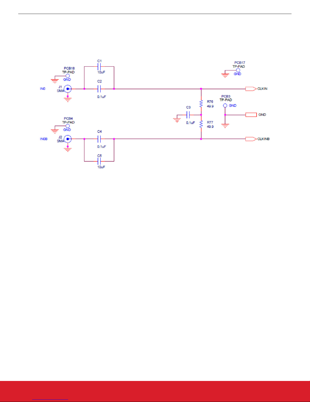
7. Clock Input Circuits (INx/INxB)
The Si5397-A-EB has eight SMA connectors (IN0, IN0B–IN3, IN3B) for receiving external clock signals. All input clocks are terminated
as shown below. Note that input clocks are ac-coupled and 50 Ω terminated. This represents four differential input clock pairs. Singleended clocks can be used by appropriately driving one side of the differential pair with a single-ended clock. For details on how to configure inputs as single-ended, please refer to the Si5397 data sheet.
Figure 7.1. Input Clock Termination Circuit
silabs.com | Building a more connected world. Rev. 0.1 | 8

UG353: Si5397 Evaluation Board User's Guide
Clock Output Circuits (OUTx/OUTxB)
8. Clock Output Circuits (OUTx/OUTxB)
Each of the sixteen output drivers (eight differential pairs, OUT0/OUT0B—OUT7/OUT7B) is ac-coupled to its respective SMA connector. The output clock termination circuit is shown below. The output signal will have no dc bias. If dc coupling is required, the ac coupling capacitors can be replaced with a resistor of appropriate value. The Si5397-A-EB provides pads for optional output termination
resistors and/or low-frequency capacitors. Note that components with a schematic “NI” designation are not normally populated on the
Si5397-A-EB and provide locations on the PCB for optional dc/ac terminations by the end user.
Figure 8.1. Output Clock Termination Circuit
silabs.com | Building a more connected world. Rev. 0.1 | 9
 Loading...