

Silicon Laboratories Si5380 User Manual

Si5380 Evaluation Board User's Guide
The Si5380-EVB is used for evaluating the Ultra Low Jitter, AnyFrequency, 12-output JESD204B Clock Generator. The Si5380
employs 4th generation DSPLL technology to enable clock generation for LTE/ JESD204B applications which require the highest level of jitter performance. The Si5380-EVB has four independent input clocks and a total of 12 outputs. The Si5380-EVB
can be easily controlled and configured using Silicon Labs’ Clock
Builder Pro™ (CBPro™) software tool.
EVB FEATURES
• Powered from USB port or external power
supply
• Onboard 54 MHz XTAL or Reference SMA
Inputs allow holdover mode of operation on
the Si5380
• CBPro™ GUI programmable VDD supply
allows device to operate from 3.3, 2.5, or
1.8 V
• CBPro™ GUI programmable VDDO
supplies allow each of the ten primary
outputs to have its own supply voltage
selectable from 3.3, 2.5, or 1.8 V
• CBPro™ GUI-controlled voltage, current,
and power measurements of VDD and all
VDDO supplies
• Status LEDs for power supplies and
control/status signals of Si5380
• SMA connectors for input clocks, output
clocks and optional external timing
reference clock
silabs.com | Smart. Connected. Energy-friendly. Rev. 1.1

Si5380 Evaluation Board User's Guide
Si5380 Functional Block Diagram
1. Si5380 Functional Block Diagram
Below is a functional block diagram of the Si5380-EVB. This EVB can be connected to a PC via the main USB connector for programming, control, and monitoring. See 2. Quick Start and Jumper Defaults or 6.1 Installing ClockBuilderPro (CBPro) Desktop Software for
more information.
Note: All Si5380 schematics, BOMs, User’s Guides, and software can be found online at the following link: http://www.silabs.com/
si538x-4x-evb
USB +5V
Connector
Ext +5V
Connector
USB Aux +5V
Connector
Ext Aux +5V
Connector
Input Clock 0
Input Clock 1
Input Clock 2
Input Clock 3
C8051F380
MCU
+
Peripherals
{
{
{
{
Power only
Power only
SPI
Conn
54 MHz
XTAL
Input
Termination
Input
Termination
Input
Termination
Input
Termination
+5V_USB
+5V_Aux
VDDMCU
I2C
I2C/SPI Bus
Control/
Status
INTR
Alarm_Status
XA
XB
CLKIN_0
CLKIN_0B
CLKIN_1
CLKIN_1B
CLKIN_2
CLKIN_2B
CLKIN_3
CLKIN_3B
Power Supply
VDD_Core
VDD_Core
VDDO_0
VDD_3.3
VDDO_0
VDD_3.3
VDDO_1
VDDO_2
VDDO_1
VDDO_2
Si5380
VDDO_3
VDDO_4
VDDO_5
VDDO_3
VDDO_4
VDDO_5
VDDO_8
VDDO_9
VDDO_6
VDDO_7
VDDO_6
VDDO_7
VDDO_8
VDDO_9
CLKOUT_0A
CLKOUT_0AB
CLKOUT_0
CLKOUT_0B
CLKOUT_1
CLKOUT_1B
CLKOUT_2
CLKOUT_2B
CLKOUT_3
CLKOUT_3B
CLKOUT_4
CLKOUT_4B
CLKOUT_5
CLKOUT_5B
CLKOUT_6
CLKOUT_6B
CLKOUT_7
CLKOUT_7B
CLKOUT_8
CLKOUT_8B
CLKOUT_9
CLKOUT_9B
CLKOUT_9A
CLKOUT_9AB
Output
Termination
Output
Termination
Output
Termination
Output
Termination
Output
Termination
Output
Termination
Output
Termination
Output
Termination
Output
Termination
Output
Termination
Output
Termination
Output
Termination
Output Clock 0A
}
Output Clock 0
}
Output Clock 1
}
Output Clock 2
}
Output Clock 3
}
Output Clock 4
}
Output Clock 5
}
Output Clock 6
}
Output Clock 7
}
Output Clock 8
}
Output Clock 9
}
Output Clock 9A
}
Figure 1.1. Functional Block Diagram of Si5380-EVB
silabs.com | Smart. Connected. Energy-friendly. Rev. 1.1 | 1

2. Quick Start and Jumper Defaults
Perform the following steps to quick-start the ClockBuilderPro software.
1. Install ClockBuilderPro desktop software. http://www.silabs.com/CBPro
2. Connect a USB cable from the Si5380-EVB to the PC where the software was installed.
3. Leave the jumpers as installed from the factory, and launch the ClockBuilderPro software.
4. You can use ClockBuilderPro to create, download, and verify a frequency plan on the Si5380-EVB.
5. For the Si5380 data sheet, go to: http://www.silabs.com/timing and search for Si5380 datasheet.
The following table lists the Si5380 EVB jumper defaults.
Table 2.1. Si5380 EVB Jumper Defaults*
Si5380 Evaluation Board User's Guide
Quick Start and Jumper Defaults
Location Type I = Installed
O= Open
JP1 2 pin O JP23 2 pin O
JP2 2 pin O JP24 3 pin all open
JP3 2 pin O JP25 2 pin O
JP4 2 pin I JP26 3 pin all open
JP5 2 pin O JP27 2 pin O
JP6 2 pin O JP28 3 pin all open
JP7 2 pin I JP29 2 pin O
JP8 2 pin O JP30 3 pin all open
JP9 2 pin O JP31 2 pin O
JP10 2 pin O JP32 3 pin all open
JP13 2 pin O JP33 2 pin O
JP14 2 pin I JP34 3 pin all open
JP15 3 pin 1 to 2 JP35 2 pin O
JP16 3 pin 1 to 2 JP36 3 pin all open
Location Type I = Installed
O= Open
JP17 2 pin O JP39 2 pin O
JP18 3 pin all open JP40 2 pin O
JP19 2 pin O JP41 2 pin O
JP20 3 pin all open
JP21 2 pin O
JP22 3 pin all open J36 5x2 Hdr All 5 installed
Note: Refer to the Si5380-EVB schematics for the functionality associated with each jumper.
silabs.com | Smart. Connected. Energy-friendly. Rev. 1.1 | 2

Si5380 Evaluation Board User's Guide
Status LEDs
3. Status LEDs
Table 3.1. Si5380 EVB Status LEDs
Location Silkscreen Color Status Function Indication
D11 INTRB Blue DUT Interrupt Active
D12 LOLB Blue DUT Loss of Lock Indicator
D21 READY Green MCU Ready
D22 3P3V Blue DUT +3.3 V is present
D24 BUSY Green MCU Busy
D25 INTR Red MCU Interrupt active
D26 VDD DUT Blue DUT VDD voltage present
D27 5VUSBMAIN Blue Main USB +5 V present
D27, D22, and D26 are illuminated when USB +5 V, Si5380 +3.3 V, and Si5380 Output +5 V supply voltages, respectively, are present.
D25, D21, and D24 are status LEDs showing on-board MCU activity. D11 and D12 are status indicators from the DUT.
Figure 3.1. Status LEDs
silabs.com | Smart. Connected. Energy-friendly. Rev. 1.1 | 3

Si5380 Evaluation Board User's Guide
External Reference Input (XA/XB)
4. External Reference Input (XA/XB)
An external reference (XTAL) is used in combination with the internal oscillator to produce an ultra-low jitter reference clock for the
DSPLL and for providing a stable reference for the free-run and holdover modes. The Si5380-EVB can also accommodate an external
reference clock instead of a crystal. To evaluate the device with a REFCLK, C111 and C113 must be populated and the XTAL removed
(see figure below). The REFCLK can then be applied to J39 and J40.
Note: The remaining components marked “NI” are not installed.
Figure 4.1. External Reference Input Circuit
silabs.com | Smart. Connected. Energy-friendly. Rev. 1.1 | 4
Si5380 Evaluation Board User's Guide
Clock Input and Output Circuits
5. Clock Input and Output Circuits
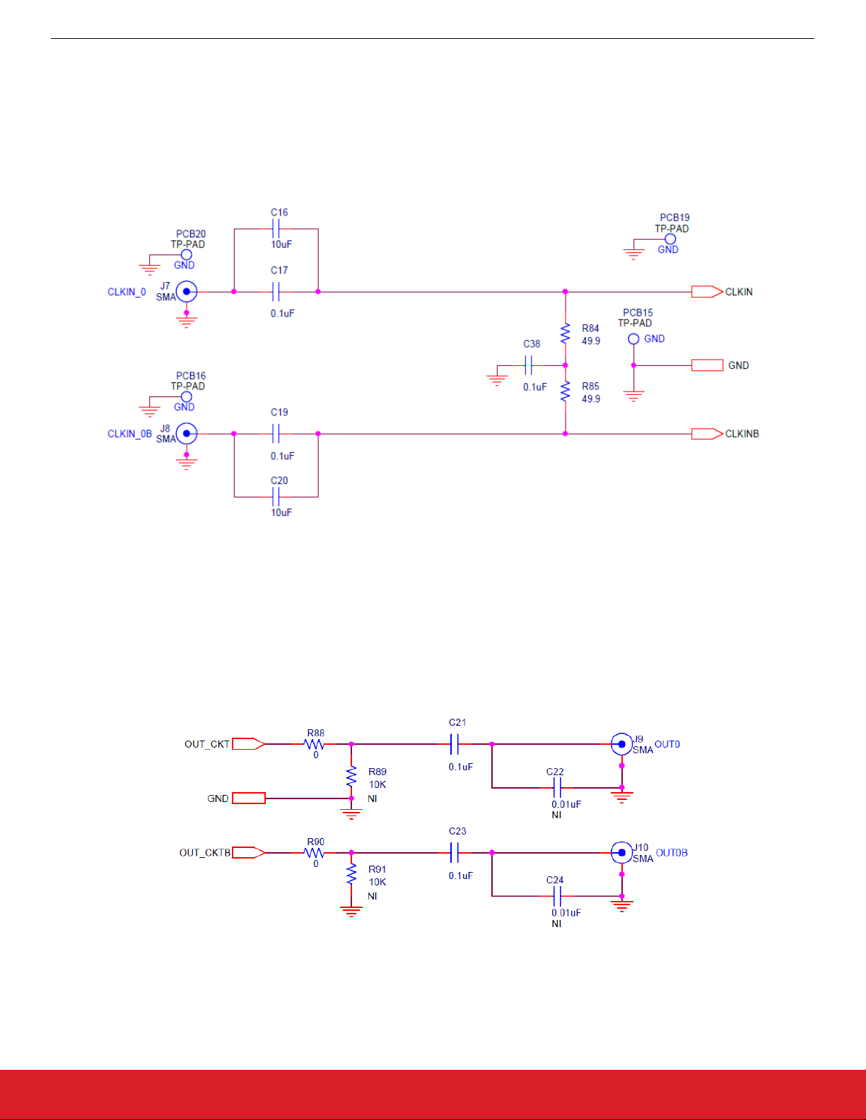
5.1 Clock Input Circuits (INx/INxB and FB_IN/FB_INB)
The Si5380-EVB has eight SMA connectors (IN0/IN0B–IN2/IN2B and IN3(FB_IN)/IN3B(FB_INB)) for receiving external clock signals.
All input clocks are terminated as shown in the figure below. Note input clocks are ac coupled and 50 Ω terminated. This represents
four differential input clock pairs. Single-ended clocks can be used by appropriately driving one side of the differential pair with a singleended clock. For details on how to configure inputs as single-ended, please refer to the Si5380 data sheet.
Figure 5.1. Input Clock Termination Circuit
5.2 Clock Output Circuits (OUTx/OUTxB)
Each of the twenty-four output drivers (12 differential pairs) is ac coupled to its respective SMA connector. The output clock termination
circuit is shown in the figure below. The output signal will have no dc bias. If dc coupling is required, the ac coupling capacitors can be
replaced with a resistor of appropriate value. The Si5380-EVB provides pads for optional output termination resistors and/or low frequency capacitors. Note that components with schematic “NI” designation are not normally populated on the Si5380-EVB, and provide
locations on the PCB for optional dc/ac terminations by the end user.
Figure 5.2. Output Clock Termination Circuit
silabs.com | Smart. Connected. Energy-friendly. Rev. 1.1 | 5

Si5380 Evaluation Board User's Guide
Using the Si5380 EVB and Installing ClockBuilderPro (CBPro) Desktop Software
6. Using the Si5380 EVB and Installing ClockBuilderPro (CBPro) Desktop Software
6.1 Installing ClockBuilderPro (CBPro) Desktop Software
To install the CBPro software on any Windows 7 (or above) PC:
Go to http://www.silabs.com/si538x-4x-evb and download the ClockBuilderPro software.
Installation instructions, release notes, and a user’s guide for ClockBuilderPro can be found at the download link shown above. Please
follow the instructions as indicated.
6.2 Connecting the EVB to Your Host PC
Once ClockBuilderPro software in installed, connect to the EVB with a USB cable as shown below.
Figure 6.1. EVB Connection Diagram
silabs.com | Smart. Connected. Energy-friendly. Rev. 1.1 | 6
 Loading...