

Page 1

ANY-FREQUENCY PRECISION CLOCKS
Si5316, Si5319, Si5322, Si5323, Si5324, Si5325,
Si5326, Si5327, Si5328, Si5365, Si5366, Si5367,
Si5368, Si5369, Si5374, Si5375, Si5376
F
AMILY REFERENCE MANUAL
Rev. 1.2 6/13 Copyright © 2013 by Silicon Laboratories Si53xx-RM
Page 2

Si53xx-RM
2 Rev. 1.2
Page 3

Si53xx-RM
TABLE OF CONTENTS
Section Page
1. Any-Frequency Precision Clock Product Family Overview . . . . . . . . . . . . . . . . . . . . . .12
2. Wideband Devices . . . . . . . . . . . . . . . . . . . . . . . . . . . . . . . . . . . . . . . . . . . . . . . . . . . . . . .15
2.1. Narrowband vs. Wideband Overview . . . . . . . . . . . . . . . . . . . . . . . . . . . . . . . . . . . .15
3. Any-Frequency Clock Family Members . . . . . . . . . . . . . . . . . . . . . . . . . . . . . . . . . . . . . .16
3.1. Si5316 . . . . . . . . . . . . . . . . . . . . . . . . . . . . . . . . . . . . . . . . . . . . . . . . . . . . . . . . . . . .16
3.2. Si5319 . . . . . . . . . . . . . . . . . . . . . . . . . . . . . . . . . . . . . . . . . . . . . . . . . . . . . . . . . . . .17
3.3. Si5322 . . . . . . . . . . . . . . . . . . . . . . . . . . . . . . . . . . . . . . . . . . . . . . . . . . . . . . . . . . . .18
3.4. Si5323 . . . . . . . . . . . . . . . . . . . . . . . . . . . . . . . . . . . . . . . . . . . . . . . . . . . . . . . . . . . .19
3.5. Si5324 . . . . . . . . . . . . . . . . . . . . . . . . . . . . . . . . . . . . . . . . . . . . . . . . . . . . . . . . . . . .20
3.6. Si5325 . . . . . . . . . . . . . . . . . . . . . . . . . . . . . . . . . . . . . . . . . . . . . . . . . . . . . . . . . . . .21
3.7. Si5326 . . . . . . . . . . . . . . . . . . . . . . . . . . . . . . . . . . . . . . . . . . . . . . . . . . . . . . . . . . . .22
3.8. Si5327 . . . . . . . . . . . . . . . . . . . . . . . . . . . . . . . . . . . . . . . . . . . . . . . . . . . . . . . . . . . .23
3.9. Si5328 . . . . . . . . . . . . . . . . . . . . . . . . . . . . . . . . . . . . . . . . . . . . . . . . . . . . . . . . . . . .24
3.10. Si5365 . . . . . . . . . . . . . . . . . . . . . . . . . . . . . . . . . . . . . . . . . . . . . . . . . . . . . . . . . . .25
3.11. Si5366 . . . . . . . . . . . . . . . . . . . . . . . . . . . . . . . . . . . . . . . . . . . . . . . . . . . . . . . . . . .26
3.12. Si5367 . . . . . . . . . . . . . . . . . . . . . . . . . . . . . . . . . . . . . . . . . . . . . . . . . . . . . . . . . . .27
3.13. Si5368 . . . . . . . . . . . . . . . . . . . . . . . . . . . . . . . . . . . . . . . . . . . . . . . . . . . . . . . . . . .28
3.14. Si5369 . . . . . . . . . . . . . . . . . . . . . . . . . . . . . . . . . . . . . . . . . . . . . . . . . . . . . . . . . . .29
3.15. Si5374/75/76 Compared to Si5324/19/26 . . . . . . . . . . . . . . . . . . . . . . . . . . . . . . . .29
3.16. Si5374 . . . . . . . . . . . . . . . . . . . . . . . . . . . . . . . . . . . . . . . . . . . . . . . . . . . . . . . . . . .30
3.17. Si5375 . . . . . . . . . . . . . . . . . . . . . . . . . . . . . . . . . . . . . . . . . . . . . . . . . . . . . . . . . . .31
3.18. Si5376 . . . . . . . . . . . . . . . . . . . . . . . . . . . . . . . . . . . . . . . . . . . . . . . . . . . . . . . . . . .32
4. DSPLL (All Devices) . . . . . . . . . . . . . . . . . . . . . . . . . . . . . . . . . . . . . . . . . . . . . . . . . . . . . .33
4.1. Clock Multiplication . . . . . . . . . . . . . . . . . . . . . . . . . . . . . . . . . . . . . . . . . . . . . . . . . .34
4.2. PLL Performance . . . . . . . . . . . . . . . . . . . . . . . . . . . . . . . . . . . . . . . . . . . . . . . . . . .35
4.2.1. Jitter Generation . . . . . . . . . . . . . . . . . . . . . . . . . . . . . . . . . . . . . . . . . . . . . . . . . . . . . . . . . . . . 35
4.2.2. Jitter Transfer. . . . . . . . . . . . . . . . . . . . . . . . . . . . . . . . . . . . . . . . . . . . . . . . . . . . . . . . . . . . . . . 35
4.2.3. Jitter Tolerance . . . . . . . . . . . . . . . . . . . . . . . . . . . . . . . . . . . . . . . . . . . . . . . . . . . . . . . . . . . . . 36
5. Pin Control Parts (Si5316, Si5322, Si5323, Si5365, Si5366) . . . . . . . . . . . . . . . . . . . . . .37
5.1. Clock Multiplication (Si5316, Si5322, Si5323, Si5365, Si5366) . . . . . . . . . . . . . . . .37
5.1.1. Clock Multiplication (Si5316) . . . . . . . . . . . . . . . . . . . . . . . . . . . . . . . . . . . . . . . . . . . . . . . . . . . 37
5.1.2. Clock Multiplication (Si5322, Si5323, Si5365, Si5366) . . . . . . . . . . . . . . . . . . . . . . . . . . . . . . . 39
5.1.3. CKOUT3 and CKOUT4 (Si5365 and Si5366) . . . . . . . . . . . . . . . . . . . . . . . . . . . . . . . . . . . . . . 51
5.1.4. Loop bandwidth (Si5316, Si5322, Si5323, Si5365, Si5366) . . . . . . . . . . . . . . . . . . . . . . . . . . . 51
5.1.5. Jitter Tolerance (Si5316, Si5323, Si5366) . . . . . . . . . . . . . . . . . . . . . . . . . . . . . . . . . . . . . . . . . 51
5.1.6. Narrowband Performance (Si5316, Si5323, Si5366). . . . . . . . . . . . . . . . . . . . . . . . . . . . . . . . . 51
5.1.7. Input-to-Output Skew (Si5316, Si5323, Si5366) . . . . . . . . . . . . . . . . . . . . . . . . . . . . . . . . . . . . 51
5.1.8. Wideband Performance (Si5322 and Si5365). . . . . . . . . . . . . . . . . . . . . . . . . . . . . . . . . . . . . . 51
5.1.9. Lock Detect (Si5322 and Si5365) . . . . . . . . . . . . . . . . . . . . . . . . . . . . . . . . . . . . . . . . . . . . . . . 51
5.1.10. Input-to-Output Skew (Si5322 and Si5365). . . . . . . . . . . . . . . . . . . . . . . . . . . . . . . . . . . . . . . 51
5.2. PLL Self-Calibration . . . . . . . . . . . . . . . . . . . . . . . . . . . . . . . . . . . . . . . . . . . . . . . . .52
5.2.1. Input Clock Stability during Internal Self-Calibration
(Si5316, Si5322, Si5323, Si5365, Si5366). . . . . . . . . . . . . . . . . . . . . . . . . . . . . . . . . . . . . . . . . 52
5.2.2. Self-Calibration caused by Changes in Input Frequency
(Si5316, Si5322, Si5323, Si5365, Si5366). . . . . . . . . . . . . . . . . . . . . . . . . . . . . . . . . . . . . . . . . 52
Rev. 1.2 3
Page 4

Si53xx-RM
5.2.3. Recommended Reset Guidelines (Si5316, Si5322, Si5323, Si5365, Si5366). . . . . . . . . . . . . . 52
5.3. Pin Control Input Clock Control . . . . . . . . . . . . . . . . . . . . . . . . . . . . . . . . . . . . . . . . .54
5.3.1. Manual Clock Selection . . . . . . . . . . . . . . . . . . . . . . . . . . . . . . . . . . . . . . . . . . . . . . . . . . . . . . . 54
5.3.2. Automatic Clock Selection (Si5322, Si5323, Si5365, Si5366). . . . . . . . . . . . . . . . . . . . . . . . . . 55
5.3.3. Hitless Switching with Phase Build-Out (Si5323, Si5366) . . . . . . . . . . . . . . . . . . . . . . . . . . . . . 56
5.4. Digital Hold/VCO Freeze . . . . . . . . . . . . . . . . . . . . . . . . . . . . . . . . . . . . . . . . . . . . . .57
5.4.1. Narrowband Digital Hold (Si5316, Si5323, Si5366). . . . . . . . . . . . . . . . . . . . . . . . . . . . . . . . . . 57
5.4.2. Recovery from Digital Hold (Si5316, Si5323, Si5366). . . . . . . . . . . . . . . . . . . . . . . . . . . . . . . . 57
5.4.3. Wideband VCO Freeze (Si5322, Si5365) . . . . . . . . . . . . . . . . . . . . . . . . . . . . . . . . . . . . . . . . . 57
5.5. Frame Synchronization (Si5366) . . . . . . . . . . . . . . . . . . . . . . . . . . . . . . . . . . . . . . . .57
5.6. Output Phase Adjust (Si5323, Si5366) . . . . . . . . . . . . . . . . . . . . . . . . . . . . . . . . . . .58
5.6.1. FSYNC Realignment (Si5366). . . . . . . . . . . . . . . . . . . . . . . . . . . . . . . . . . . . . . . . . . . . . . . . . . 58
5.6.2. Including FSYNC Inputs in Clock Selection (Si5366) . . . . . . . . . . . . . . . . . . . . . . . . . . . . . . . . 58
5.6.3. FS_OUT Polarity and Pulse Width Control (Si5366) . . . . . . . . . . . . . . . . . . . . . . . . . . . . . . . . . 58
5.6.4. Using FS_OUT as a Fifth Output Clock (Si5366) . . . . . . . . . . . . . . . . . . . . . . . . . . . . . . . . . . . 58
5.6.5. Disabling FS_OUT (Si5366) . . . . . . . . . . . . . . . . . . . . . . . . . . . . . . . . . . . . . . . . . . . . . . . . . . . 59
5.7. Output Clock Drivers . . . . . . . . . . . . . . . . . . . . . . . . . . . . . . . . . . . . . . . . . . . . . . . . .59
5.7.1. LVPECL and CMOS TQFP Output Signal Format Restrictions at 3.3 V (Si5365, Si5366) . . . . 59
5.8. PLL Bypass Mode . . . . . . . . . . . . . . . . . . . . . . . . . . . . . . . . . . . . . . . . . . . . . . . . . . .60
5.9. Alarms . . . . . . . . . . . . . . . . . . . . . . . . . . . . . . . . . . . . . . . . . . . . . . . . . . . . . . . . . . . .60
5.9.1. Loss-of-Signal Alarms (Si5316, Si5322, Si5323, Si5365, Si5366) . . . . . . . . . . . . . . . . . . . . . . 60
5.9.2. FOS Alarms (Si5365 and Si5366) . . . . . . . . . . . . . . . . . . . . . . . . . . . . . . . . . . . . . . . . . . . . . . . 60
5.9.3. FSYNC Align Alarm (Si5366 and CK_CONF = 1 and FRQTBL = L) . . . . . . . . . . . . . . . . . . . . . 61
5.9.4. C1B and C2B Alarm Outputs (Si5316, Si5322, Si5323) . . . . . . . . . . . . . . . . . . . . . . . . . . . . . . 61
5.9.5. C1B, C2B, C3B, and ALRMOUT Outputs (Si5365, Si5366) . . . . . . . . . . . . . . . . . . . . . . . . . . . 61
5.10. Device Reset . . . . . . . . . . . . . . . . . . . . . . . . . . . . . . . . . . . . . . . . . . . . . . . . . . . . . .62
5.11. DSPLLsim Configuration Software . . . . . . . . . . . . . . . . . . . . . . . . . . . . . . . . . . . . .62
6. Microprocessor Controlled Parts (Si5319, Si5324, Si5325, Si5326, Si5327, Si5328,
Si5367, Si5368, Si5369, Si5374, Si5375, and Si5376) . . . . . . . . . . . . . . . . . . . . . . . . . . .63
6.1. Clock Multiplication . . . . . . . . . . . . . . . . . . . . . . . . . . . . . . . . . . . . . . . . . . . . . . . . . .63
6.1.1. Jitter Tolerance (Si5319, Si5324, Si5325, Si5326, Si5327, Si5328,
Si5368, Si5369, Si5374, Si5375, and Si5376). . . . . . . . . . . . . . . . . . . . . . . . . . . . . . . . . . . . . . 63
6.1.2. Wideband Parts (Si5325, Si5367) . . . . . . . . . . . . . . . . . . . . . . . . . . . . . . . . . . . . . . . . . . . . . . . 63
6.1.3. Narrowband Parts (Si5319, Si5324, Si5326, Si5327, Si5328, Si5368,
Si5369, Si5374, Si5375, and Si5376) . . . . . . . . . . . . . . . . . . . . . . . . . . . . . . . . . . . . . . . . . . . . 64
6.1.4. Loop Bandwidth (Si5319, Si5326, Si5368, Si5375, and Si5376). . . . . . . . . . . . . . . . . . . . . . . . 66
6.1.5. Lock Detect (Si5319, Si5326, Si5327, Si5328, Si5368, Si5369, Si5374,
Si5375, and Si5376) . . . . . . . . . . . . . . . . . . . . . . . . . . . . . . . . . . . . . . . . . . . . . . . . . . . . . . . . . 66
6.2. PLL Self-Calibration . . . . . . . . . . . . . . . . . . . . . . . . . . . . . . . . . . . . . . . . . . . . . . . . .66
6.2.1. Initiating Internal Self-Calibration. . . . . . . . . . . . . . . . . . . . . . . . . . . . . . . . . . . . . . . . . . . . . . . . 67
6.2.2. Input Clock Stability during Internal Self-Calibration . . . . . . . . . . . . . . . . . . . . . . . . . . . . . . . . . 67
6.2.3. Self-Calibration Caused by Changes in Input Frequency . . . . . . . . . . . . . . . . . . . . . . . . . . . . . 67
6.2.4. Narrowband Input-to-Output Skew (Si5319, Si5324, Si5326, Si5327,
Si5328, Si5368, Si5369, Si5374, Si5375, and Si5376) . . . . . . . . . . . . . . . . . . . . . . . . . . . . . . . . . . . . 67
6.2.5. Clock Output Behavior Before and During ICAL (Si5319, Si5324, Si5326,
Si5327, Si5328, Si5368, Si5369, Si5374, Si5375, and Si5376) . . . . . . . . . . . . . . . . . . . . . . . . 68
6.3. Input Clock Configurations (Si5367 and Si5368) . . . . . . . . . . . . . . . . . . . . . . . . . . .69
6.4. Input Clock Control . . . . . . . . . . . . . . . . . . . . . . . . . . . . . . . . . . . . . . . . . . . . . . . . . .69
6.4.1. Manual Clock Selection (Si5324, Si5325, Si5326, Si5328, Si5367, Si5368,
Si5369, Si5374, and Si5376). . . . . . . . . . . . . . . . . . . . . . . . . . . . . . . . . . . . . . . . . . . . . . . . . . . 70
6.4.2. Automatic Clock Selection (Si5324, Si5325, Si5326, Si5328, Si5367, Si5368,
Si5369, Si5374, and Si5376). . . . . . . . . . . . . . . . . . . . . . . . . . . . . . . . . . . . . . . . . . . . . . . . . . . 71
4 Rev. 1.2
Page 5

Si53xx-RM
6.4.3. Hitless Switching with Phase Build-Out (Si5324, Si5326, Si5327, Si5328,
Si5368, Si5369, Si5374, and Si5376) . . . . . . . . . . . . . . . . . . . . . . . . . . . . . . . . . . . . . . . . . . . . 72
6.5. Si5319, Si5324, Si5326, Si5327, Si5328, Si5368, Si5369, Si5374,
Si5375, and Si5376 Free Run Mode . . . . . . . . . . . . . . . . . . . . . . . . . . . . . . . . .73
6.5.1. Free Run Mode Programming Procedure . . . . . . . . . . . . . . . . . . . . . . . . . . . . . . . . . . . . . . . . . 73
6.5.2. Clock Control Logic in Free Run Mode . . . . . . . . . . . . . . . . . . . . . . . . . . . . . . . . . . . . . . . . . . . 73
6.5.3. Free Run Reference Frequency Constraints . . . . . . . . . . . . . . . . . . . . . . . . . . . . . . . . . . . . . . . 74
6.5.4. Free Run Reference Frequency Constraints . . . . . . . . . . . . . . . . . . . . . . . . . . . . . . . . . . . . . . . 74
6.6. Digital Hold . . . . . . . . . . . . . . . . . . . . . . . . . . . . . . . . . . . . . . . . . . . . . . . . . . . . . . . .75
6.6.1. Narrowband Digital Hold (Si5316, Si5324, Si5326, Si5328, Si5368,
Si5369, Si5374, Si5376) . . . . . . . . . . . . . . . . . . . . . . . . . . . . . . . . . . . . . . . . . . . . . . . . . . . . . . 75
6.6.2. History Settings for Low Bandwidth Devices (Si5324, Si5327, Si5328,
Si5369, Si5374). . . . . . . . . . . . . . . . . . . . . . . . . . . . . . . . . . . . . . . . . . . . . . . . . . . . . . . . . . . . . 77
6.6.3. Recovery from Digital Hold (Si5319, Si5324, Si5326, Si5327, Si5328,
Si5368, Si5369, Si5374, and Si5376) . . . . . . . . . . . . . . . . . . . . . . . . . . . . . . . . . . . . . . . . . . . . 77
6.6.4. VCO Freeze (Si5319, Si5325, Si5367, Si5375). . . . . . . . . . . . . . . . . . . . . . . . . . . . . . . . . . . . . 77
6.6.5. Digital Hold versus VCO Freeze . . . . . . . . . . . . . . . . . . . . . . . . . . . . . . . . . . . . . . . . . . . . . . . . 77
6.7. Output Phase Adjust (Si5326, Si5368) . . . . . . . . . . . . . . . . . . . . . . . . . . . . . . . . . . .78
6.7.1. Coarse Skew Control (Si5326, Si5368) . . . . . . . . . . . . . . . . . . . . . . . . . . . . . . . . . . . . . . . . . . . 78
6.7.2. Fine Skew Control (Si5326, Si5368) . . . . . . . . . . . . . . . . . . . . . . . . . . . . . . . . . . . . . . . . . . . . . 78
6.7.3. Independent Skew (Si5324, Si5326, Si5328, Si5368, Si5369, Si5374, and Si5376) . . . . . . . . 79
6.7.4. Output-to-output Skew (Si5324, Si5326, Si5327, Si5328, Si5368,
Si5369, Si5374, and Si5376). . . . . . . . . . . . . . . . . . . . . . . . . . . . . . . . . . . . . . . . . . . . . . . . . . . 79
6.7.5. Input-to-Output Skew (All Devices) . . . . . . . . . . . . . . . . . . . . . . . . . . . . . . . . . . . . . . . . . . . . . . 79
6.8. Frame Synchronization Realignment (Si5368 and CK_CONFIG_REG = 1) . . . . . . .79
6.8.1. FSYNC Realignment (Si5368). . . . . . . . . . . . . . . . . . . . . . . . . . . . . . . . . . . . . . . . . . . . . . . . . . 81
6.8.2. FSYNC Skew Control (Si5368) . . . . . . . . . . . . . . . . . . . . . . . . . . . . . . . . . . . . . . . . . . . . . . . . . 82
6.8.3. Including FSYNC Inputs in Clock Selection (Si5368) . . . . . . . . . . . . . . . . . . . . . . . . . . . . . . . . 82
6.8.4. FS_OUT Polarity and Pulse Width Control (Si5368) . . . . . . . . . . . . . . . . . . . . . . . . . . . . . . . . . 82
6.8.5. Using FS_OUT as a Fifth Output Clock (Si5368) . . . . . . . . . . . . . . . . . . . . . . . . . . . . . . . . . . . 82
6.9. Output Clock Drivers (Si5319, Si5324, Si5325, Si5326, Si5327,
Si5328, Si5367, Si5368, Si5369, Si5374, Si5375, Si5376) . . . . . . . . . . . . . . . . . . . .83
6.9.1. Disabling CKOUTn. . . . . . . . . . . . . . . . . . . . . . . . . . . . . . . . . . . . . . . . . . . . . . . . . . . . . . . . . . . 83
6.9.2. LVPECL TQFP Output Signal Format Restrictions at 3.3 V (Si5367, Si5368, Si5369). . . . . . . 83
6.10. PLL Bypass Mode (Si5319, Si5324, Si5325, Si5326, Si5327, Si5328,
Si5367, Si5368, Si5369, Si5374, Si5375, and Si5376) . . . . . . . . . . . . . . . . . . . . . .84
6.11. Alarms (Si5319, Si5324, Si5325, Si5326, Si5327, Si5328, Si5367,
Si5368, Si5369, Si5374, Si5375, and Si5376) . . . . . . . . . . . . . . . . . . . . . . . . . . . .84
6.11.1. Loss-of-Signal Alarms (Si5319, Si5324, Si5325, Si5326, Si5327, Si5328,
Si5367, Si5368, Si5369, Si5374, Si5375, and Si5376) . . . . . . . . . . . . . . . . . . . . . . . . . . . . . . 84
6.11.2. FOS Algorithm (Si5324, Si5325, Si5326, Si5328, Si5368, Si5369, Si5374, and Si5376 ). . . . 85
6.11.3. C1B, C2B (Si5319, Si5324, Si5325, Si5326, Si5327, Si5328, Si5374,
Si5375, and Si5376) . . . . . . . . . . . . . . . . . . . . . . . . . . . . . . . . . . . . . . . . . . . . . . . . . . . . . . . . 87
6.11.4. LOS (Si5319, Si5375) . . . . . . . . . . . . . . . . . . . . . . . . . . . . . . . . . . . . . . . . . . . . . . . . . . . . . . . 87
6.11.5. C1B, C2B, C3B, ALRMOUT (Si5367, Si5368, Si5369 [CK_CONFIG_REG = 0]) . . . . . . . . . . 87
6.11.6. C1B, C2B, C3B, ALRMOUT (Si5368 [CK_CONFIG_REG = 1]) . . . . . . . . . . . . . . . . . . . . . . . 88
6.11.7. LOS Algorithm for Reference Clock Input (Si5319, Si5324, Si5326, Si5327,
Si5328, Si5368, Si5369, Si5374, Si5375, and Si5376). . . . . . . . . . . . . . . . . . . . . . . . . . . . . . 89
6.11.8. LOL (Si5319, Si5324, Si5326, Si5327, Si5328, Si5368, Si5369, Si5374,
Si5375, and Si5376) . . . . . . . . . . . . . . . . . . . . . . . . . . . . . . . . . . . . . . . . . . . . . . . . . . . . . . . . 89
6.11.9. Device Interrupts . . . . . . . . . . . . . . . . . . . . . . . . . . . . . . . . . . . . . . . . . . . . . . . . . . . . . . . . . . . 89
Rev. 1.2 5
Page 6

Si53xx-RM
6.12. Device Reset . . . . . . . . . . . . . . . . . . . . . . . . . . . . . . . . . . . . . . . . . . . . . . . . . . . . . .89
6.13. I2C Serial Microprocessor Interface . . . . . . . . . . . . . . . . . . . . . . . . . . . . . . . . . . . .90
6.14. Serial Microprocessor Interface (SPI) . . . . . . . . . . . . . . . . . . . . . . . . . . . . . . . . . . .91
6.14.1. Default Device Configuration. . . . . . . . . . . . . . . . . . . . . . . . . . . . . . . . . . . . . . . . . . . . . . . . . . 93
6.15. Register Descriptions . . . . . . . . . . . . . . . . . . . . . . . . . . . . . . . . . . . . . . . . . . . . . . .93
6.16. DSPLLsim Configuration Software . . . . . . . . . . . . . . . . . . . . . . . . . . . . . . . . . . . . .93
7. High-Speed I/O . . . . . . . . . . . . . . . . . . . . . . . . . . . . . . . . . . . . . . . . . . . . . . . . . . . . . . . . . .94
7.1. Input Clock Buffers . . . . . . . . . . . . . . . . . . . . . . . . . . . . . . . . . . . . . . . . . . . . . . . . . .94
7.2. Output Clock Drivers . . . . . . . . . . . . . . . . . . . . . . . . . . . . . . . . . . . . . . . . . . . . . . . . .96
7.2.1. LVPECL TQFP Output Signal Format Restrictions at 3.3 V (Si5367, Si5368, Si5369). . . . . . . 96
7.2.2. Typical Output Circuits. . . . . . . . . . . . . . . . . . . . . . . . . . . . . . . . . . . . . . . . . . . . . . . . . . . . . . . . 96
7.2.3. Typical Clock Output Scope Shots . . . . . . . . . . . . . . . . . . . . . . . . . . . . . . . . . . . . . . . . . . . . . . 98
7.3. Typical Scope Shots for SFOUT Options . . . . . . . . . . . . . . . . . . . . . . . . . . . . . . . . .99
7.4. Crystal/Reference Clock Interfaces (Si5316, Si5319, Si5323, Si5324, Si5326,
Si5327, Si5328, Si5366, Si5368, Si5369, Si5374, Si5375, and Si5376) . . . . . . . .102
7.5. Three-Level (3L) Input Pins (No External Resistors) . . . . . . . . . . . . . . . . . . . . . . .104
7.6. Three-Level (3L) Input Pins (With External Resistors) . . . . . . . . . . . . . . . . . . . . . .105
8. Power Supply . . . . . . . . . . . . . . . . . . . . . . . . . . . . . . . . . . . . . . . . . . . . . . . . . . . . . . . . . .106
9. Packages and Ordering Guide . . . . . . . . . . . . . . . . . . . . . . . . . . . . . . . . . . . . . . . . . . . .107
Appendix A—Narrowband References . . . . . . . . . . . . . . . . . . . . . . . . . . . . . . . . . . . . . . .108
Appendix B—Frequency Plans and Typical Jitter Performance (Si5316,
Si5319, Si5323, Si5324, Si5326, Si5327, Si5366, Si5368, Si5369,
Si5374, Si5375, and Si5376) . . . . . . . . . . . . . . . . . . . . . . . . . . . . . . . . . . . . .112
Appendix C—Typical Phase Noise Plots . . . . . . . . . . . . . . . . . . . . . . . . . . . . . . . . . . . . . .119
Appendix D—Alarm Structure . . . . . . . . . . . . . . . . . . . . . . . . . . . . . . . . . . . . . . . . . . . . . . .137
Appendix E—Internal Pullup, Pulldown by Pin . . . . . . . . . . . . . . . . . . . . . . . . . . . . . . . . .140
Appendix F—Typical Performance: Bypass Mode, PSRR, Crosstalk,
Output Format Jitter . . . . . . . . . . . . . . . . . . . . . . . . . . . . . . . . . . . . . . . . . . .147
Appendix G—Near Integer Ratios . . . . . . . . . . . . . . . . . . . . . . . . . . . . . . . . . . . . . . . . . . . .155
Appendix H—Jitter Attenuation and Loop BW . . . . . . . . . . . . . . . . . . . . . . . . . . . . . . . . .157
Appendix I—Response to a Frequency Step Function . . . . . . . . . . . . . . . . . . . . . . . . . . .162
Appendix J—Si5374, Si5375, Si5376 PCB Layout Recommendations . . . . . . . . . . . . . .163
Appendix K—Si5374, Si5375, and Si5376 Crosstalk . . . . . . . . . . . . . . . . . . . . . . . . . . . . .167
Appendix L—Jitter Transfer and Peaking . . . . . . . . . . . . . . . . . . . . . . . . . . . . . . . . . . . . .174
Document Change List . . . . . . . . . . . . . . . . . . . . . . . . . . . . . . . . . . . . . . . . . . . . . . . . . . . .177
Contact Information . . . . . . . . . . . . . . . . . . . . . . . . . . . . . . . . . . . . . . . . . . . . . . . . . . . . . . .17 8
6 Rev. 1.2
Page 7

Si53xx-RM
LIST OF FIGURES
Figure 1. Si5316 Any-Frequency Jitter Attenuator Block Diagram . . . . . . . . . . . . . . . . . . . . . 16
Figure 2. Si5319 Any-Frequency Jitter Attenuating Clock Multiplier Block Diagram . . . . . . . .17
Figure 3. Si5322 Low Jitter Clock Multiplier Block Diagram . . . . . . . . . . . . . . . . . . . . . . . . . . 18
Figure 4. Si5323 Jitter Attenuating Clock Multiplier Block Diagram . . . . . . . . . . . . . . . . . . . . 19
Figure 5. Si5324 Clock Multiplier and Jitter Attenuator Block Diagram. . . . . . . . . . . . . . . . . . 20
Figure 6. Si5325 Low Jitter Clock Multiplier Block Diagram . . . . . . . . . . . . . . . . . . . . . . . . . . 21
Figure 7. Si5326 Clock Multiplier and Jitter Attenuator Block Diagram. . . . . . . . . . . . . . . . . . 22
Figure 8. Si5327 Clock Multiplier and Jitter Attenuator Block Diagram. . . . . . . . . . . . . . . . . . 23
Figure 9. Si5328 Clock Multiplier and Jitter Attenuator Block Diagram. . . . . . . . . . . . . . . . . . 24
Figure 10. Si5365 Low Jitter Clock Multiplier Block Diagram . . . . . . . . . . . . . . . . . . . . . . . . . 25
Figure 11. Si5366 Jitter Attenuating Clock Multiplier Block Diagram . . . . . . . . . . . . . . . . . . . 26
Figure 12. Si5367 Clock Multiplier Block Diagram . . . . . . . . . . . . . . . . . . . . . . . . . . . . . . . . . 27
Figure 13. Si5368 Clock Multiplier and Jitter Attenuator Block Diagram. . . . . . . . . . . . . . . . . 28
Figure 14. Si5369 Clock Multiplier and Jitter Attenuator Block Diagram. . . . . . . . . . . . . . . . . 29
Figure 15. Si5374 Functional Block Diagram . . . . . . . . . . . . . . . . . . . . . . . . . . . . . . . . . . . . . 30
Figure 16. Si5375 Functional Block Diagram . . . . . . . . . . . . . . . . . . . . . . . . . . . . . . . . . . . . . 31
Figure 17. Si5376 Functional Block Diagram . . . . . . . . . . . . . . . . . . . . . . . . . . . . . . . . . . . . . 32
Figure 18. Any-Frequency Precision Clock DSPLL Block Diagram . . . . . . . . . . . . . . . . . . . . 33
Figure 19. Clock Multiplication Circuit . . . . . . . . . . . . . . . . . . . . . . . . . . . . . . . . . . . . . . . . . . . 34
Figure 20. PLL Jitter Transfer Mask/Template . . . . . . . . . . . . . . . . . . . . . . . . . . . . . . . . . . . . 35
Figure 21. Jitter Tolerance Mask/Template. . . . . . . . . . . . . . . . . . . . . . . . . . . . . . . . . . . . . . . 36
Figure 22. Si5316 Divisor Ratios. . . . . . . . . . . . . . . . . . . . . . . . . . . . . . . . . . . . . . . . . . . . . . . 38
Figure 23. Wideband PLL Divider Settings (Si5325, Si5367) . . . . . . . . . . . . . . . . . . . . . . . . . 63
Figure 24. Narrowband PLL Divider Settings (Si5319, Si5324, Si5326, Si5327,
Si5328, Si5368, Si5369, Si5374, Si5375, and Si5376) . . . . . . . . . . . . . . . . . . . . . 65
Figure 25. Si5324, Si5325, Si5326, Si5327, Si5328, Si5374, and Si5376
Input Clock Selection. . . . . . . . . . . . . . . . . . . . . . . . . . . . . . . . . . . . . . . . . . . . . . . 69
Figure
Figure 27. Free Run Mode Block Diagram . . . . . . . . . . . . . . . . . . . . . . . . . . . . . . . . . . . . . . . .73
Figure 28. Parameters in History Value of M . . . . . . . . . . . . . . . . . . . . . . . . . . . . . . . . . . . . . 75
Figure 29. Digital Hold vs. VCO Freeze Example . . . . . . . . . . . . . . . . . . . . . . . . . . . . . . . . . . 77
Figure 30. Frame Sync Frequencies. . . . . . . . . . . . . . . . . . . . . . . . . . . . . . . . . . . . . . . . . . . . 80
Figure 31. FOS Compare . . . . . . . . . . . . . . . . . . . . . . . . . . . . . . . . . . . . . . . . . . . . . . . . . . . . 86
Figure 32. I
Figure 33. I2C Example. . . . . . . . . . . . . . . . . . . . . . . . . . . . . . . . . . . . . . . . . . . . . . . . . . . . . . 90
Figure 34. SPI Write/Set Address Command . . . . . . . . . . . . . . . . . . . . . . . . . . . . . . . . . . . . . 92
Figure 35. SPI Read Command . . . . . . . . . . . . . . . . . . . . . . . . . . . . . . . . . . . . . . . . . . . . . . . 92
Figure 36. SPI Timing Diagram. . . . . . . . . . . . . . . . . . . . . . . . . . . . . . . . . . . . . . . . . . . . . . . . 93
Figure 37. Differential LVPECL Termination. . . . . . . . . . . . . . . . . . . . . . . . . . . . . . . . . . . . . . 94
Figure 38. Single-Ended LVPECL Termination. . . . . . . . . . . . . . . . . . . . . . . . . . . . . . . . . . . . 94
Figure 39. CML/LVDS Termination (1.8, 2.5, 3.3 V) . . . . . . . . . . . . . . . . . . . . . . . . . . . . . . . . 95
Figure 40. Center Tap Bypassed Termination . . . . . . . . . . . . . . . . . . . . . . . . . . . . . . . . . . . . 95
Figure 41. CMOS Termination (1.8, 2.5, 3.3 V). . . . . . . . . . . . . . . . . . . . . . . . . . . . . . . . . . . . 95
26. Si5367, Si5368, and Si5369 Input Clock Selection . . . . . . . . . . . . . . . . . . . . . . . . 70
2
C Command Format . . . . . . . . . . . . . . . . . . . . . . . . . . . . . . . . . . . . . . . . . . . . . . 90
Rev. 1.2 7
Page 8

Si53xx-RM
Figure 42. Typical Output Circuit (Differential) . . . . . . . . . . . . . . . . . . . . . . . . . . . . . . . . . . . . 96
Figure 43. Differential Output Example Requiring Attenuation . . . . . . . . . . . . . . . . . . . . . . . . 97
Figure 44. Typical CMOS Output Circuit (Tie CKOUTn+ and CKOUTn– Together). . . . . . . . 97
Figure 45. Differential CKOUT Structure (not for CMOS) . . . . . . . . . . . . . . . . . . . . . . . . . . . . 98
Figure 46. sfout_2, CMOS. . . . . . . . . . . . . . . . . . . . . . . . . . . . . . . . . . . . . . . . . . . . . . . . . . . . 99
Figure 47. sfout_3, lowSwingLVDS. . . . . . . . . . . . . . . . . . . . . . . . . . . . . . . . . . . . . . . . . . . . . 99
Figure 48. sfout_5, LVPECL . . . . . . . . . . . . . . . . . . . . . . . . . . . . . . . . . . . . . . . . . . . . . . . . . 100
Figure 49. sfout_6, CML . . . . . . . . . . . . . . . . . . . . . . . . . . . . . . . . . . . . . . . . . . . . . . . . . . . . 100
Figure 50. sfout_7, LVDS . . . . . . . . . . . . . . . . . . . . . . . . . . . . . . . . . . . . . . . . . . . . . . . . . . . 101
Figure 51. CMOS External Reference Circuit . . . . . . . . . . . . . . . . . . . . . . . . . . . . . . . . . . . . 102
Figure 52. Sinewave External Clock Circuit . . . . . . . . . . . . . . . . . . . . . . . . . . . . . . . . . . . . . 102
Figure 53. Differential External Reference Input Example
(Not for Si5374, Si5375, or Si5376) . . . . . . . . . . . . . . . . . . . . . . . . . . . . . . . . . . .103
Figure 54. Differential OSC Reference Input Example for Si5374, Si5375 and Si5376 . . . . .103
Figure 55. Three Level Input Pins. . . . . . . . . . . . . . . . . . . . . . . . . . . . . . . . . . . . . . . . . . . . . 104
Figure 56. Three Level Input Pins. . . . . . . . . . . . . . . . . . . . . . . . . . . . . . . . . . . . . . . . . . . . . 105
Figure 57. Typical Power Supply Bypass Network (TQFP Package) . . . . . . . . . . . . . . . . . . 106
Figure 58. Typical Power Supply Bypass Network (QFN Package) . . . . . . . . . . . . . . . . . . . 106
Figure 59. Typical Reference Jitter Transfer Function . . . . . . . . . . . . . . . . . . . . . . . . . . . . . 111
Figure 60. Phase Noise vs. f3 . . . . . . . . . . . . . . . . . . . . . . . . . . . . . . . . . . . . . . . . . . . . . . . .112
Figure 61. Jitter Integrated from 12 kHz to 20 MHz Jitter, fs RMS . . . . . . . . . . . . . . . . . . . . 113
Figure 62. Jitter Integrated from 100 Hz to 40 MHz Jitter, fs RMS . . . . . . . . . . . . . . . . . . . . 114
Figure 63. Jitter vs. f3 with FPGA . . . . . . . . . . . . . . . . . . . . . . . . . . . . . . . . . . . . . . . . . . . . . 115
Figure 64. Reference vs. Output Frequency. . . . . . . . . . . . . . . . . . . . . . . . . . . . . . . . . . . . . 116
Figure 65. 622.08 MHz Output with a 114.285 MHz Crystal. . . . . . . . . . . . . . . . . . . . . . . . . 117
Figure 66. 622.08 MHz Output with a 40 MHz Crystal . . . . . . . . . . . . . . . . . . . . . . . . . . . . . 118
Figure 67. 155.52 MHz In; 622.08 MHz Out . . . . . . . . . . . . . . . . . . . . . . . . . . . . . . . . . . . . . .119
Figure 68. 155.52 MHz In; 622.08 MHz Out; Loop BW = 7 Hz, Si5324 . . . . . . . . . . . . . . . . .120
Figure 69. 19.44 MHz In; 156.25 MHz Out; Loop BW = 80 Hz . . . . . . . . . . . . . . . . . . . . . . .121
Figure 70. 19.44 MHz In; 156.25 MHz Out; Loop BW = 5 Hz, Si5324 . . . . . . . . . . . . . . . . . .122
Figure 71. 27 MHz In; 148.35 MHz Out; Light Trace BW = 6 Hz;
Dark Trace BW = 110 Hz, Si5324 . . . . . . . . . . . . . . . . . . . . . . . . . . . . . . . . . . . . .123
Figure 72. 61.44 MHz In; 491.52 MHz Out; Loop BW = 7 Hz, Si5324 . . . . . . . . . . . . . . . . . .124
Figure 73. 622.08 MHz In; 672.16 MHz Out; Loop BW = 6.9 kHz . . . . . . . . . . . . . . . . . . . . .125
Figure 74. 622.08 MHz In; 672.16 MHz Out; Loop BW = 100 Hz . . . . . . . . . . . . . . . . . . . . .126
Figure 75. 156.25 MHz In; 155.52 MHz Out . . . . . . . . . . . . . . . . . . . . . . . . . . . . . . . . . . . . . .127
Figure 76. 78.125 MHz In; 644.531 MHz Out . . . . . . . . . . . . . . . . . . . . . . . . . . . . . . . . . . . . .128
Figure 77. 78.125 MHz In; 690.569 MHz Out . . . . . . . . . . . . . . . . . . . . . . . . . . . . . . . . . . . . .129
Figure 78. 78.125 MHz In; 693.493 MHz Out . . . . . . . . . . . . . . . . . . . . . . . . . . . . . . . . . . . . 130
Figure 79. 86.685 MHz In; 173.371 MHz and 693.493 MHz Out . . . . . . . . . . . . . . . . . . . . . 131
Figure 80. 86.685 MHz In; 173.371 MHz Out . . . . . . . . . . . . . . . . . . . . . . . . . . . . . . . . . . . . 132
Figure 81. 86.685 MHz In; 693.493 MHz Out . . . . . . . . . . . . . . . . . . . . . . . . . . . . . . . . . . . . 133
Figure 82. 155.52 MHz and 156.25 MHz In; 622.08 MHz Out . . . . . . . . . . . . . . . . . . . . . . . 134
Figure 83. 10 MHz In; 1 GHz Out . . . . . . . . . . . . . . . . . . . . . . . . . . . . . . . . . . . . . . . . . . . . . 135
Figure 84. Si5324, Si5326, and Si5328 Alarm Diagram . . . . . . . . . . . . . . . . . . . . . . . . . . . . 137
Figure 85. Si5368 and Si5369 Alarm Diagram (1 of 2) . . . . . . . . . . . . . . . . . . . . . . . . . . . . . 138
8 Rev. 1.2
Page 9

Si53xx-RM
Figure 86. Si5368 and Si5369 Alarm Diagram (2 of 2) . . . . . . . . . . . . . . . . . . . . . . . . . . . . . 139
Figure 87. ±50 ppm, 2 ppm Steps . . . . . . . . . . . . . . . . . . . . . . . . . . . . . . . . . . . . . . . . . . . . .155
Figure 88. ±200 ppm, 10 ppm Steps. . . . . . . . . . . . . . . . . . . . . . . . . . . . . . . . . . . . . . . . . . . 156
Figure 89. ±2000 ppm, 50 ppm Steps. . . . . . . . . . . . . . . . . . . . . . . . . . . . . . . . . . . . . . . . . . 156
Figure 90. RF Generator, Si5326, Si5324; No Jitter (For Reference) . . . . . . . . . . . . . . . . . .158
Figure 91. RF Generator, Si5326, Si5324 (50 Hz Jitter). . . . . . . . . . . . . . . . . . . . . . . . . . . . 158
Figure 92. RF Generator, Si5326, Si5324 (100 Hz Jitter) . . . . . . . . . . . . . . . . . . . . . . . . . . . 159
Figure 93. RF Generator, Si5326, Si5324 (500 Hz Jitter) . . . . . . . . . . . . . . . . . . . . . . . . . . . 159
Figure 94. RF Generator, Si5326, Si5324 (1 kHz Jitter). . . . . . . . . . . . . . . . . . . . . . . . . . . . 160
Figure 95. RF Generator, Si5326, Si5324 (5 kHz Jitter). . . . . . . . . . . . . . . . . . . . . . . . . . . . 160
Figure 96. RF Generator, Si5326, Si5324 (10 kHz Jitter). . . . . . . . . . . . . . . . . . . . . . . . . . . 161
Figure 97. Si5326 Frequency Step Function Response . . . . . . . . . . . . . . . . . . . . . . . . . . . . 162
Figure 98. Vdd Plane . . . . . . . . . . . . . . . . . . . . . . . . . . . . . . . . . . . . . . . . . . . . . . . . . . . . . . .163
Figure 99. Ground Plane and Reset . . . . . . . . . . . . . . . . . . . . . . . . . . . . . . . . . . . . . . . . . . . .164
Figure 100. Output Clock Routing. . . . . . . . . . . . . . . . . . . . . . . . . . . . . . . . . . . . . . . . . . . . . 165
Figure 101. OSC_P, OSC_N Routing. . . . . . . . . . . . . . . . . . . . . . . . . . . . . . . . . . . . . . . . . . 166
Figure 102. Si5374, Si5375, and Si5376 DSPLL A. . . . . . . . . . . . . . . . . . . . . . . . . . . . . . . . 168
Figure 103. Si5374, Si5375, and Si5376 DSPLL B. . . . . . . . . . . . . . . . . . . . . . . . . . . . . . . . 169
Figure 104. Si5374, Si5375, and Si5376 DSPLL C. . . . . . . . . . . . . . . . . . . . . . . . . . . . . . . . 170
Figure 105. Si5374, Si5375, and Si5376 DSPLL D. . . . . . . . . . . . . . . . . . . . . . . . . . . . . . . . 171
Figure 106. Example Frequency Plan Sources. . . . . . . . . . . . . . . . . . . . . . . . . . . . . . . . . . . 172
Figure 107. Run Time Frequency Plan Examples. . . . . . . . . . . . . . . . . . . . . . . . . . . . . . . . . 173
Figure 108. Wide View of Jitter Transfer . . . . . . . . . . . . . . . . . . . . . . . . . . . . . . . . . . . . . . . .174
Figure 109. Zoomed View of Jitter Transfer . . . . . . . . . . . . . . . . . . . . . . . . . . . . . . . . . . . . . 175
Figure 110. Zoomed Again View of Jitter Transfer (Showing Peaking). . . . . . . . . . . . . . . . . 175
Figure 111. Maximum Zoomed View of Jitter Peaking . . . . . . . . . . . . . . . . . . . . . . . . . . . . . 176
Rev. 1.2 9
Page 10

Si53xx-RM
LIST OF TABLES
Table 1. Product Selection Guide . . . . . . . . . . . . . . . . . . . . . . . . . . . . . . . . . . . . . . . . . . . . . . 14
Table 2. Product Selection Guide (Si5322/25/65/67) . . . . . . . . . . . . . . . . . . . . . . . . . . . . . . . 15
Table 3. Si5316, Si5322, Si5323, Si5365 and Si5366 Key Features . . . . . . . . . . . . . . . . . . . 37
Table 4. Frequency Settings . . . . . . . . . . . . . . . . . . . . . . . . . . . . . . . . . . . . . . . . . . . . . . . . . . 37
Table 5. Input Divider Settings . . . . . . . . . . . . . . . . . . . . . . . . . . . . . . . . . . . . . . . . . . . . . . . . 38
Table 6. Si5316 Bandwidth Values . . . . . . . . . . . . . . . . . . . . . . . . . . . . . . . . . . . . . . . . . . . . . 38
Table 7. SONET Clock Multiplication Settings (FRQTBL=L) . . . . . . . . . . . . . . . . . . . . . . . . . 39
Table 8. Datacom Clock Multiplication Settings (FRQTBL = M, CK_CONF = 0) . . . . . . . . . . 44
Table 9. SONET to Datacom Clock Multiplication Settings. . . . . . . . . . . . . . . . . . . . . . . . . . . 48
Table 10. Clock Output Divider Control (DIV34) . . . . . . . . . . . . . . . . . . . . . . . . . . . . . . . . . . . 51
Table 11. Si5316, Si5322, and Si5323 Pins and Reset . . . . . . . . . . . . . . . . . . . . . . . . . . . . . 53
Table 12. Si5365 and Si5366 Pins and Reset. . . . . . . . . . . . . . . . . . . . . . . . . . . . . . . . . . . . . 53
Table 13. Manual Input Clock Selection (Si5316, Si5322, Si5323), AUTOSEL = L . . . . . . . . 54
Table 14. Manual Input Clock Selection (Si5365, Si5366), AUTOSEL = L. . . . . . . . . . . . . . . 54
Table 15. Automatic/Manual Clock Selection . . . . . . . . . . . . . . . . . . . . . . . . . . . . . . . . . . . . . 55
Table 16. Clock Active Indicators (AUTOSEL = M or H) (Si5322 and Si5323). . . . . . . . . . . . 55
Table 17. Clock Active Indicators (AUTOSEL = M or H) (Si5365 and Si5367). . . . . . . . . . . . 55
Table 18. Input Clock Priority for Auto Switching (Si5322, Si5323) . . . . . . . . . . . . . . . . . . . . 55
Table 19. Input Clock Priority for Auto Switching (Si5365, Si5366) . . . . . . . . . . . . . . . . . . . . 56
Table 20. FS_OUT Disable Control (DBLFS) . . . . . . . . . . . . . . . . . . . . . . . . . . . . . . . . . . . . . 59
Table 21. Output Signal Format Selection (SFOUT). . . . . . . . . . . . . . . . . . . . . . . . . . . . . . . . 59
Table 22. DSBL2/BYPASS Pin Settings . . . . . . . . . . . . . . . . . . . . . . . . . . . . . . . . . . . . . . . . . 60
Table 23. Frequency Offset Control (FOS_CTL). . . . . . . . . . . . . . . . . . . . . . . . . . . . . . . . . . . 61
Table 24. Alarm Output Logic Equations. . . . . . . . . . . . . . . . . . . . . . . . . . . . . . . . . . . . . . . . . 61
Table 25. Lock Detect Retrigger Time. . . . . . . . . . . . . . . . . . . . . . . . . . . . . . . . . . . . . . . . . . . 62
Table 26. Narrowband Frequency Limits . . . . . . . . . . . . . . . . . . . . . . . . . . . . . . . . . . . . . . . . 65
Table 27. Dividers and Limi
Table 28. CKOUT_ALWAYS_ON and SQ_ICAL Truth Table. . . . . . . . . . . . . . . . . . . . . . . . . 68
Table 29. Manual Input Clock Selection (Si5367, Si5368, Si5369). . . . . . . . . . . . . . . . . . . . . 70
Table 30. Manual Input Clock Selection (Si5324, Si5325, Si5326, Si5328,
Si5374, and Si5376) . . . . . . . . . . . . . . . . . . . . . . . . . . . . . . . . . . . . . . . . . . . . . . . . 71
Table 31. Automatic/Manual Clock Selection . . . . . . . . . . . . . . . . . . . . . . . . . . . . . . . . . . . . . 71
Table 32. Input Clock Priority for Auto Switching . . . . . . . . . . . . . . . . . . . . . . . . . . . . . . . . . . 72
Table 33. Digital Hold History Delay . . . . . . . . . . . . . . . . . . . . . . . . . . . . . . . . . . . . . . . . . . . . 76
Table 34. Digital Hold History Averaging Time . . . . . . . . . . . . . . . . . . . . . . . . . . . . . . . . . . . . 76
Table 35. CKIN3/CKIN4 Frequency Selection (CK_CONF = 1) . . . . . . . . . . . . . . . . . . . . . . . 80
Table 36. Common NC5 Divider Settings . . . . . . . . . . . . . . . . . . . . . . . . . . . . . . . . . . . . . . . . 81
Table 37. Alignment Alarm Trigger Threshold. . . . . . . . . . . . . . . . . . . . . . . . . . . . . . . . . . . . . 81
Table 38. Output Signal Format Selection . . . . . . . . . . . . . . . . . . . . . . . . . . . . . . . . . . . . . . . 83
Table 39. Loss-of-Signal Validation Times . . . . . . . . . . . . . . . . . . . . . . . . . . . . . . . . . . . . . . . 84
Table 40. Loss-of-Signal Registers. . . . . . . . . . . . . . . . . . . . . . . . . . . . . . . . . . . . . . . . . . . . . 84
Table 41. FOS Reference Clock Selection . . . . . . . . . . . . . . . . . . . . . . . . . . . . . . . . . . . . . . . 86
ts . . . . . . . . . . . . . . . . . . . . . . . . . . . . . . . . . . . . . . . . . . . . . . . . . 65
10 Rev. 1.2
Page 11

Si53xx-RM
Table 42. CLKnRATE Registers . . . . . . . . . . . . . . . . . . . . . . . . . . . . . . . . . . . . . . . . . . . . . . . 86
Table 43. Alarm Output Logic Equations (Si5367, Si5368, and Si5369
[CONFIG_REG = 0]) . . . . . . . . . . . . . . . . . . . . . . . . . . . . . . . . . . . . . . . . . . . . . . . . 88
Table 44. Alarm Output Logic Equations [Si5368 and CKCONFIG_REG = 1] . . . . . . . . . . . . 88
Table 45. Lock Detect Retrigger Time (LOCKT). . . . . . . . . . . . . . . . . . . . . . . . . . . . . . . . . . . 89
Table 46. SPI Command Format. . . . . . . . . . . . . . . . . . . . . . . . . . . . . . . . . . . . . . . . . . . . . . . 91
Table 47. Output Driver Configuration. . . . . . . . . . . . . . . . . . . . . . . . . . . . . . . . . . . . . . . . . . . 96
Table 48. Disabling Unused Output Driver . . . . . . . . . . . . . . . . . . . . . . . . . . . . . . . . . . . . . . . 97
Table 49. Output Format Measurements1,2 . . . . . . . . . . . . . . . . . . . . . . . . . . . . . . . . . . . . . . 98
Table 50. Approved 114.285 MHz Crystals. . . . . . . . . . . . . . . . . . . . . . . . . . . . . . . . . . . . . . 108
Table 51. XA/XB Reference Sources and Frequencies . . . . . . . . . . . . . . . . . . . . . . . . . . . . 110
Table 52. Jitter vs.f3 in fs, RMS1,2,3 . . . . . . . . . . . . . . . . . . . . . . . . . . . . . . . . . . . . . . . . . . . 114
Table 53. Jitter Values for Figure 63. . . . . . . . . . . . . . . . . . . . . . . . . . . . . . . . . . . . . . . . . . . 115
Table 54. Jitter Values for Figure 64. . . . . . . . . . . . . . . . . . . . . . . . . . . . . . . . . . . . . . . . . . . 116
Table 55. Jitter Values for Figure 74 . . . . . . . . . . . . . . . . . . . . . . . . . . . . . . . . . . . . . . . . . . 128
Table 56. Jitter Values for Figure 75. . . . . . . . . . . . . . . . . . . . . . . . . . . . . . . . . . . . . . . . . . . 129
Table 57. Jitter Values for Figure 76. . . . . . . . . . . . . . . . . . . . . . . . . . . . . . . . . . . . . . . . . . . 130
Table 58. Jitter Values for Figure 77. . . . . . . . . . . . . . . . . . . . . . . . . . . . . . . . . . . . . . . . . . . 131
Table 59. Jitter Values for Figure 80. . . . . . . . . . . . . . . . . . . . . . . . . . . . . . . . . . . . . . . . . . . 134
Table 60. Si5316 Pullup/Down . . . . . . . . . . . . . . . . . . . . . . . . . . . . . . . . . . . . . . . . . . . . . . . 140
Table 61. Si5322 Pullup/Down . . . . . . . . . . . . . . . . . . . . . . . . . . . . . . . . . . . . . . . . . . . . . . . 140
Table 62. Si5323 Pullup/Down . . . . . . . . . . . . . . . . . . . . . . . . . . . . . . . . . . . . . . . . . . . . . . . 141
Table 63. Si5319, Si5324, Si5328 Pullup/Down . . . . . . . . . . . . . . . . . . . . . . . . . . . . . . . . . . 141
Table 64. Si5325 Pullup/Down . . . . . . . . . . . . . . . . . . . . . . . . . . . . . . . . . . . . . . . . . . . . . . . 142
Table 65. Si5326 Pullup/Down . . . . . . . . . . . . . . . . . . . . . . . . . . . . . . . . . . . . . . . . . . . . . . . 142
Table 66. Si5327 Pullup/Down . . . . . . . . . . . . . . . . . . . . . . . . . . . . . . . . . . . . . . . . . . . . . . . 143
Table 67. Si5365 Pullup/Down . . . . . . . . . . . . . . . . . . . . . . . . . . . . . . . . . . . . . . . . . . . . . . . 143
Table 68. Si5366 Pullup/Down . . . . . . . . . . . . . . . . . . . . . . . . . . . . . . . . . . . . . . . . . . . . . . . 144
Table 69. Si5367 Pullup/Down . . . . . . . . . . . . . . . . . . . . . . . . . . . . . . . . . . . . . . . . . . . . . . . 145
Table 70. Si5368 Pullup/Down . . . . . . . . . . . . . . . . . . . . . . . . . . . . . . . . . . . . . . . . . . . . . . . 145
Table 71. Si5369 Pullup/Down . . . . . . . . . . . . . . . . . . . . . . . . . . . . . . . . . . . . . . . . . . . . . . . 146
Table 72. Si5374/75/76 Pullup/Down . . . . . . . . . . . . . . . . . . . . . . . . . . . . . . . . . . . . . . . . . . 146
Table 73. Output Format vs. Jitter . . . . . . . . . . . . . . . . . . . . . . . . . . . . . . . . . . . . . . . . . . . . 154
Table 74. Jitter Values. . . . . . . . . . . . . . . . . . . . . . . . . . . . . . . . . . . . . . . . . . . . . . . . . . . . . . 157
Table 75. Si5374/75/76 Crosstalk Jitter Values . . . . . . . . . . . . . . . . . . . . . . . . . . . . . . . . . .
167
Rev. 1.2 11
Page 12

Si53xx-RM
1. Any-Frequency Precision Clock Product Family Overview
Silicon Laboratories Any-Frequency Precision Clock products provide jitter attenuation and clock multiplication/
clock division for applications requiring sub 1 ps rms jitter performance. The device product family is based on
Silicon Laboratories' 3rd generation DSPLL technology, which provides any-frequency synthesis and jitter
attenuation in a highly integr ated PLL solution that eliminates the need for discrete VCXO/VCSOs and loop filter
components. These devices are ideally suited for applications which require low jitter reference clocks, including
OTN (OTU-1, OTU-2, OTU-3, OTU-4), OC-48/STM-16, OC-192/STM-64, OC-768/STM-256, GbE, 10GbE, Fibre
Channel, 10GFC, synchronous Ethernet, wireless backhaul, wireless point-point infrastructure, broadcast video/
HDTV (HD SDI, 3G SDI), test and measurement, data acquisition systems, and FPGA/ASIC reference clocking.
Table 1 provides a product selector guide for the Silicon Laboratories Any-Frequency Precision Clocks. Three
product families are available. The Si5316, Si5319, Si5323, Si5324, Si5326, Si5366, and Si5368 are jitterattenuating clock multipliers that provide ultra-low jitter generation as low as 0.30 ps RMS. The devices vary
according to the number of clock inputs, number of clock outputs, and control method. The Si5316 is a fixedfrequency, pin controlled jitter attenuator that can be used in clock smoothin g applications. The Si532 3 and Si536 6
are pin-controlled jitter-attenuating clock multipliers. The frequency plan for these pin-controlled devices is
selectable from frequency lookup tables and includes common frequency translations for SONET/SDH, ITU G.709
Forward Error Correction (FEC) applications (255/238, 255/237, 255/236, 238/255, 237/255, 236/255), Gigabit
Ethernet, 10G Ethernet, 1G/2G/4G/8G/10G Fibre Channel, ATM and broadcast video (Genlock). The Si5319,
Si5324, Si5326, Si5327, Si5328, Si5368, and Si5369 are microprocessor-controlled devices that can be controlled
via an I
710 MHz and generate multiple independent, synchronous clock outputs ranging from 2 kHz to 945 MHz and
select frequencies to 1.4 GHz. Virtually any frequency translation combination across this operating range is
supported. Independent dividers are available for every input clock and output clock, so the Si5324, Si5326,
Si5327, Si5328, and Si5368 can accept input clocks at different frequencies and generate output clocks at different
frequencies. The Si5316, Si5319, Si5323, Si5326, Si5366, Si5368, and Si5369 support a digitally programmable
loop bandwidth that can range from 60 Hz to 8.4 kHz. An external (37–41 MHz, 55–61 MHz, and 109–125.5 MHz)
reference clock or a low-cost 114.285 MHz 3rd overtone crystal is required for these devices to enable ultra-low
jitter generation and jitter attenuation. (See "Appendix A—Narrowband References" on page 108.) The Si5324,
Si5327, and Si5369 are much lower bandwidth devices, providing a user-programmable loop bandwidth from 4 to
525 Hz. The Si5328 is an ultra-low-loop BW device that is intended for SyncE timing card applications (G.8262)
with loop BW values of from 0.05 to 6 Hz.
The Si5323, Si5324, Si5326, Si5327, Si5328, Si5366, Si5368, and Si5369 support hitless switching between input
clocks in compliance with GR-253-CORE and GR-1244-CORE that greatly minimizes the propagation of phase
transients to the clock outputs during an input clock transition (<200 ps typ). Manual, automatic revertive and
automatic non-revertive input clock switching options are available. The devices monitor the input clocks for lossof-signal and provide a LOS alarm when missing pulses on any of the input clocks are detected. The devices
monitor the lock status of the PLL and provide a LOL alarm when the PLL is unlocked. The lock detect algorithm
works by continuously monitoring the phase of the selected input clock in relation to the phase of the feedback
clock. The Si5324, Si5326, Si5328, Si5366, Si5368, and Si5369 monitor the frequency of the input clocks with
respect to a reference frequency applied to an input clock or the XA/XB input, and generates a frequency offset
alarm (FOS) if the threshold is exceeded. This FOS feature is available for SONET/SDH applications. Both Stratum
3/3E and SONET Minimum Clock (SMC) FOS thresholds are supported.
The Si5319, Si5323, Si5324, Si5326, Si5328, Si5366, Si5368, and Si5369 provide a digital hold capability that
allows the device to continue gen eration of a s table output clock when the select ed input refe rence is los t. During
digital hold, the DSPLL generates an o utput frequency base d on a histor ical average tha t existed a fixed amount of
time before the error event occurred, eliminating the effects of phase and frequency transients that may occur
immediately preceding entry into digital hold.
The Si5322, Si5325, Si5365, and Si5367 are frequency flexible, low jitter clock multipliers that provide jitter
generation of 0.6 ps RMS without jitter attenuation. These devices provide low jitter integer clock multiplication or
fractional clock synthesis, but they are not as frequency-flexible as the Si5319/23/24/26/66/68/69. The devices
vary according to the number of clock inputs, number of clock ou tput s, and co ntrol method . The Si5322 and Si5365
are pin-controlled clock multipliers. The frequency plan for these devices is selectable from frequency lookup
2
C or SPI interface. These microprocessor-controlled devices accept clock inputs ranging from 2 kHz to
12 Rev. 1.2
Page 13

Si53xx-RM
tables.
A wide range of settings are available, but they are a subset of the frequency plans supported by the Si5323 and
Si5366 jitter-attenuating clock multipliers. The Si5325 and Si5367 are microprocessor-controlled clock multipliers
that can be controlled via an I
These devices accept clock inputs ranging from 10 MHz to 710 MHz and generate multiple independent,
synchronous clock outputs ranging from 10 MHz to 945 MHz and select frequencies to 1.4 GHz. The Si5325 and
Si5367 support a subset of the frequen cy translations available in the Si5319, Si5 324, Si5326, Si5327, Si5 368, and
Si5369 jitter-attenuating clock multipliers. The Si5325 and Si5367 can accept input clocks at different frequencies
and generate output clocks at different frequencies. The Si5322, Si5325, Si5365, and Si5367 support a digitally
programmable loop bandwidth that ranges from 150 kHz to 1.3 MHz. No external components are required for
these devices. LOS and FOS monitoring is available for these devices, as described above.
The Si5374, Si5375, and Si5376 are quad DSPLL versions of the Si5324, Si5319, and Si5326, respectively. Each
of the four DSPLLs can oper ate at comple tely independ ent frequencies. The only resources that they share are a
common I
reference source. Since they require a require a free standing reference oscillator, the XA/XB reference pins were
renamed to OSC_P and OSC_N. The Si5375 consists of four one-input and one-output DSPLLs. The Si5374
consists of four two-input and two-output DSPLLs with very low loop bandwid th. The Si5376 is similar to the Si5374
with the exception that it has higher loop BW values.
The Any-Frequency Precision Clocks have dif fere ntial clock ou tp ut(s) with pr ogr ammab le sign al for mats to support
LVPECL, LVDS, CML, and CMOS loads. If the CMOS signal format is selected, each differential output buffer
generates two in-phase CMOS clocks at the same frequency. For system-level debugging, a PLL bypass mode
drives the clock output directly from the selected input clock, bypassing the internal PLL.
Silicon Laboratories offers a PC-based software utility, DSPLLsim, that can be used to determine valid frequency
plans and loop bandwidth settings for the Any-Frequency Precision Clock product family. For the microprocessorcontrolled devices, DSPLLsim provides the optimum PLL divider settings for a given input frequency/clock
multiplication ratio combination that minimizes phase noise and power consumption. Two DSPLLsim configuration
software applications are available for the 1-PLL and 4-PLL devices, respectively. DSPLLsim can also be used to
simplify device selection and configuration. This utility can be downloaded from http://www.silabs.com/timing.
Other useful documentation, including device data sheets and programming files for the microprocessor-controlled
devices are available from this website.
2
C bus and a common XA/XB jitter reference oscillator. These quad devices cannot use a crystal as their
2
C or SPI interface.
Rev. 1.2 13
Page 14
Si53xx-RM
Table 1. Product Selection Guide
Part
Number
Si5315 Pin 1PLL, 2 | 2 0.008–644 0.008–644 0.45 ps
Si5316 Pin 1PLL, 2 | 1 19–710 19–710 0.3 ps
Si5317 Pin 1PLL, 1 | 2 1–710 1–710 0.3 ps
Si5319 I
Si5323 Pin 1PLL, 2 | 2 0.008–707 0.008–1050 0.3 ps
Si5324 I
Si5326 I2C/SPI 1PLL, 2 | 2 0.002–710 0.002–1417 0.3 ps
Si5327 I2C/SPI 1PLL, 2 | 2 0.002–710 0.002–808 0.5 ps
Si5328 I
Control Number of
Inputs and
Outputs
2
C/SPI 1PLL, 1 | 1 0.002–710 0.002–1417 0.3 ps
2
C/SPI 1PLL, 2 | 2 0.002–710 0.002–1417 0.3 ps
2
C/SPI 1PLL, 2 | 2 0.008–346 0.002–346 0.35 ps
Input
Frequency
(MHz)
*
Output
Frequency
(MHz)
*
RMS Phase Jitter
(12kHz–20MHz)
PLL
Bandwidth
60 Hz to
8kHz
60 Hz to
8kHz
60 Hz to
8kHz
60 Hz to
8kHz
60 Hz to
8kHz
4 Hz to
525 Hz
60 Hz to
8kHz
4 Hz to
525 Hz
0.05 Hz to
6Hz
Hitless
Switching
Free
Run
Mode
Package
6x6 mm
36-QFN
6x6 mm
36-QFN
6x6 mm
36-QFN
6x6 mm
36-QFN
6x6 mm
36-QFN
6x6 mm
36-QFN
6x6 mm
36-QFN
6x6 mm
36-QFN
6x6 mm
36-QFN
Si5366 Pin 1PLL, 4 | 5 0.008–707 0.008–1050 0.3 ps
Si5368 I2C/SPI 1PLL, 4 | 5 0.002–710 0.002–1417 0.3 ps
2
Si5369 I
Si5374 I2C 4PLL, 8 | 8 0.002–710 0.002–808 0.4 ps
Si5375 I2C 4PLL, 4 | 4 0.002–710 0.002–808 0.4 ps
Si5376 I
*Note: Maximum input and output rates may be limited by speed rating of device. See each device’s data sheet for ordering
C/SPI 1PLL, 4 | 5 0.002–710 0.002–1417 0.3 ps
2
C 4PLL, 8 | 8 0.002–710 0.002–808 0.4 ps
information.
60 Hz to
8kHz
60 Hz to
8kHz
4 Hz to
525 Hz
4 Hz to
525 Hz
60 Hz to
8kHz
60 Hz to
8kHz
14x14 mm
100-TQFP
14x14 mm
100-TQFP
14x14 mm
100-TQFP
10x10 mm
80-BGA
10x10 mm
80-BGA
10x10 mm
80-BGA
14 Rev. 1.2
Page 15
Si53xx-RM
2. Wideband Devices
These are not recommended for new designs. For alternatives, see the Si533x family of products.
Table 2. Product Selection Guide (Si5322/25/65/67)
*
Device
Low Jitter Precision Clock Multipliers (Wideband)
Si5322 2 2 707 1050 0.6 ps rms typ
Si5325 2 2
Si5365 4 5 707 1050 0.6 ps rms typ
Si5367 4 5
*Note: Maxi mum input and output rates may be limited by speed rating of device. See each device’s data sheet for ordering
information.
Clock Inputs
Clock Outputs
P Control
Max Input Freq (MHz)
Max Output Frequency (MHz)
Jitter Generation
(12 kHz – 20 MHz)
LOS
Hitless Switching
FOS Alarm
LOL Alarm
FSYNC Realignment
36 Lead 6 mm x 6 mm QFN
100 Lead 14 x 14 mm TQFP
1.8, 2.5, 3.3 V Operation
1.8, 2.5 V Operation
710 1400 0.6 ps rms typ
710 1400 0.6 ps rms typ
2.1. Narrowband vs. Wideband Overview
The narrowband (NB) devices offer a number of features and capabilities that are not available with the wideband
(WB) devices, as outlined in the below list:
Broader set of frequency plans due to more divisor options
Hitless switching between input clocks
Lower minimum input clock frequency
Lower loop bandwidth
Digital Hold (reference-based holdover instead of VCO freeze)
FRAMESYNC realignment
CLAT and FLAT (input to output skew adjust)
INC and DEC pins
PLL Loss of Lock status indicator
FOS is not supported.
Rev. 1.2 15
Page 16
Si53xx-RM
2
DSPLL
®
C1B
CS
LOL
BWSEL[1:0]
DBL_BY
Xtal or Refclock
SFOUT[1:0]
CKOUT+
CKOUT–
CKIN_1+
CKIN_1–
CKIN_2+
CKIN_2–
Control
Signal
Detect
VDD
GND
Frequency
Control
Bandwidth
Control
C2B
2
FRQSEL[1:0]
RST
0
1
RATE[1:0]
XA
XB
f
OSC
2
0
1
÷ N31
÷ N32
f
3_1
f
3_2
CK1DIV
CK2DIV
f
3
3. Any-Frequency Clock Family Members
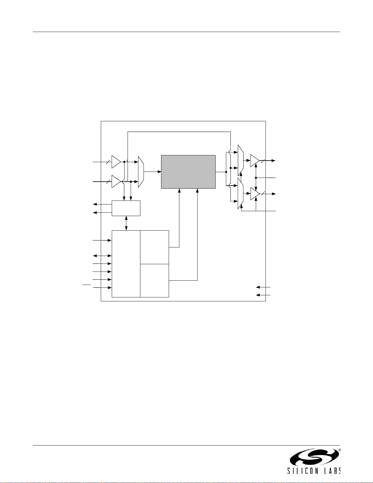
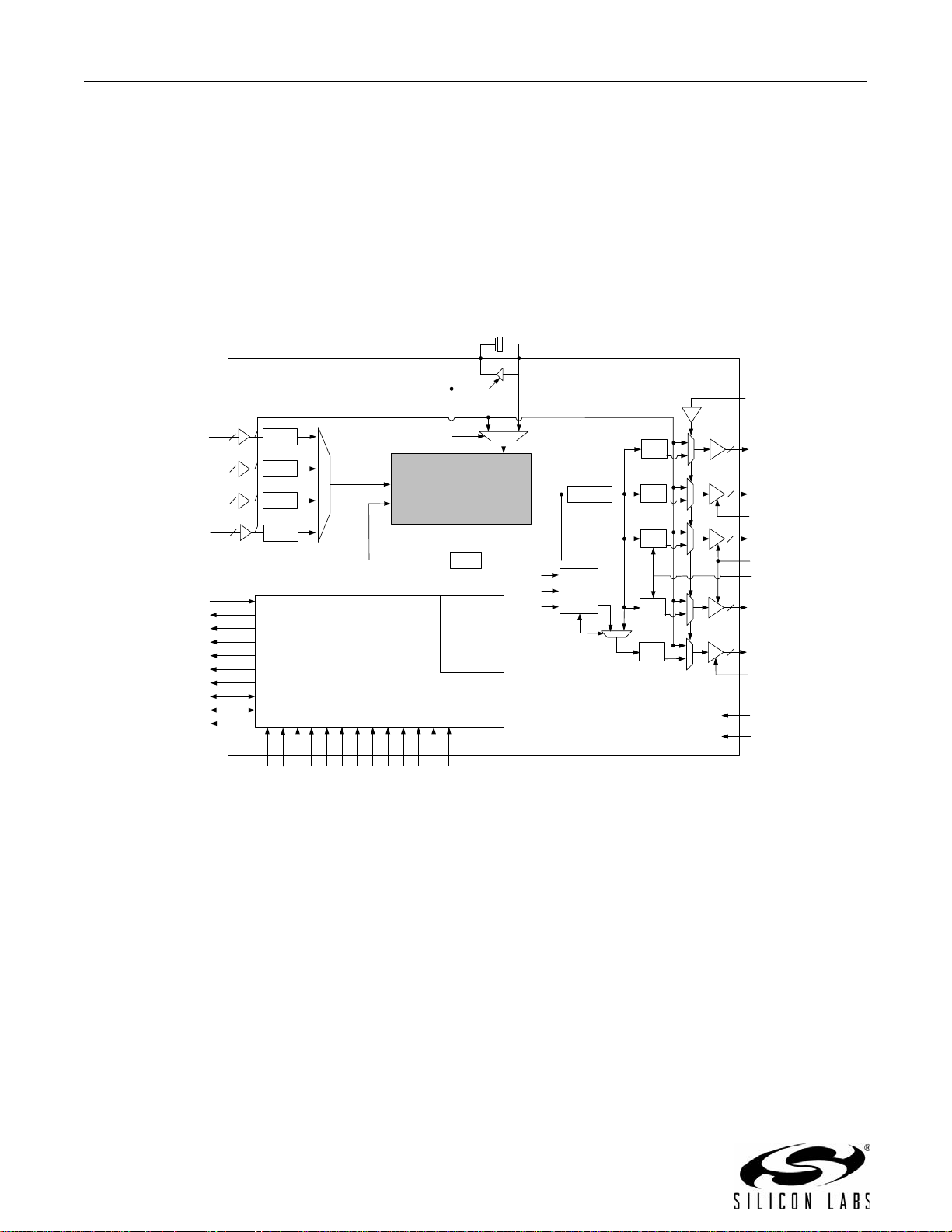
3.1. Si5316
The Si5316 is a low jitter, precision jitter attenuator for high-speed communication systems, including OC -48, OC192, 10G Ethernet, and 10G Fibre Channel. The Si5316 accepts dual clock inputs in the 19, 38, 77, 155, 311, or
622 MHz frequency range and generates a jitter-attenuated clock output at the same frequency. Within each of
these clock ranges, the device can be tuned approximately 14% higher tha n nomin al SONET/SDH fre quencies, up
to a maximum of 710 MHz in the 622 MHz range. The DSPLL loop bandwidth is digitally selec table, pr ov idin g jitte r
performance optimization at the application level. Operating fr om a single 1.8, 2.5, or 3.3 V supply, the Si5316 is
ideal for providing jitter attenuation in high performance timing applications. See "5. Pin Control Parts (Si5316,
Si5322, Si5323, Si5365, Si5366)" on page 37 for a complete description.
Figure 1. Si5316 Any-Frequency Jitter Attenuator Block Diagram
16 Rev. 1.2
Page 17
Si53xx-RM
DSPLL
®
Loss of Signal
Xtal or Refclock
CKIN
CKOUT
÷ N31
÷ N2
Signal Detect
Device Interrupt
VDD
GND
Loss of Lock
Xtal/Clock Select
I
2
C/SPI Port
Control
Rate Select
÷ N32
XO
f
3
÷ N1_HS ÷ NC1
3.2. Si5319
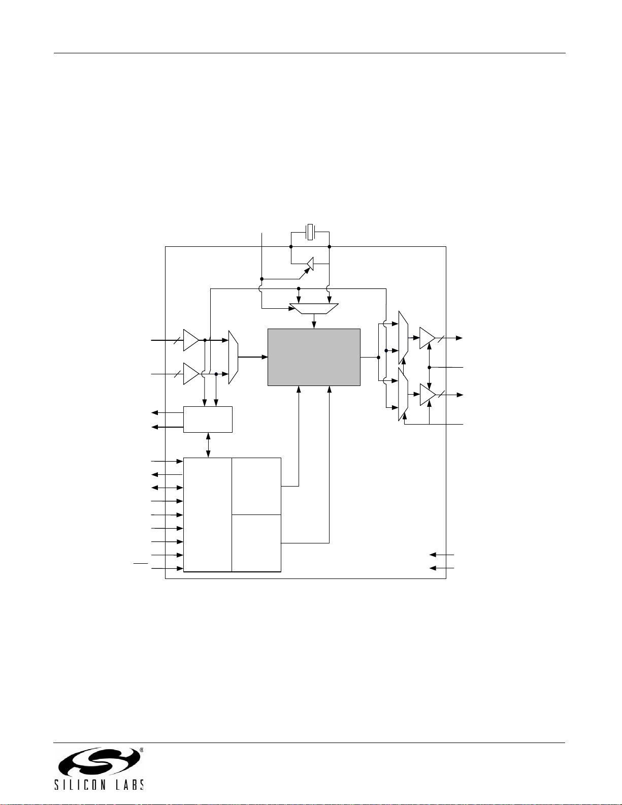
The Si5319 is a jitter-attenuating precision M/N clock multiplier for applications requiring sub 1 ps jitter
performance. The Si5319 accepts one clock input ranging from 2 kHz to 710 MHz and generates one clock output
ranging from 2 kHz to 945 MHz and select frequencies to 1.4 GHz. The Si5319 can also use its crystal oscillator as
a clock source for frequency synthesis. The device provides virtua lly any frequency translation combination across
this operating range. The Si5319 input clock frequency and clock multiplication r atio are programmable through an
I2C or SPI interface. The Si5319 is based on Silicon Laboratories' 3rd-generation DSPLL
provides any-frequency synthesis and jitter attenuation in a highly integrated PLL solution that eliminates the need
for external VCXO and loop filter components. The DSPLL loop bandwidth is digitally programmable, providing
jitter performance optimization at the application level. Operating from a single 1.8, 2.5, or 3.3 V supply, the Si5319
is ideal for providing clock multiplication and jitter attenuation in high performance timing applications. See "6.
Microprocessor Controlled Parts (Si5319, Si5324, Si5325, Si5326, Si5327, Si5328, Si5367, Si5368, Si5369,
Si5374, Si5375, and Si5376)" on page 63 for a comp lete description.
®
technology, which
Figure 2. Si5319 Any-Frequency Jitter Attenuating Clock Multiplier Block Diagram
Rev. 1.2 17
Page 18
Si53xx-RM
DSPLL
®
C1B
CS_CA
BWSEL[1:0]
DBL2_BY
SFOUT[1:0]
CKOUT_2+
CKOUT_2–
CKIN_1+
CKIN_1–
CKOUT_1+
CKOUT_2–
CKIN_2+
CKIN_2–
Control
AUTOSEL
FRQTBL
Signal
Detect
VDD
GND
Frequency
Control
Bandwidth
Control
C2B
2
2
FRQSEL[3:0]
RST
0
1
f
OSC
2
2
0
1
0
1
f
3
3.3. Si5322
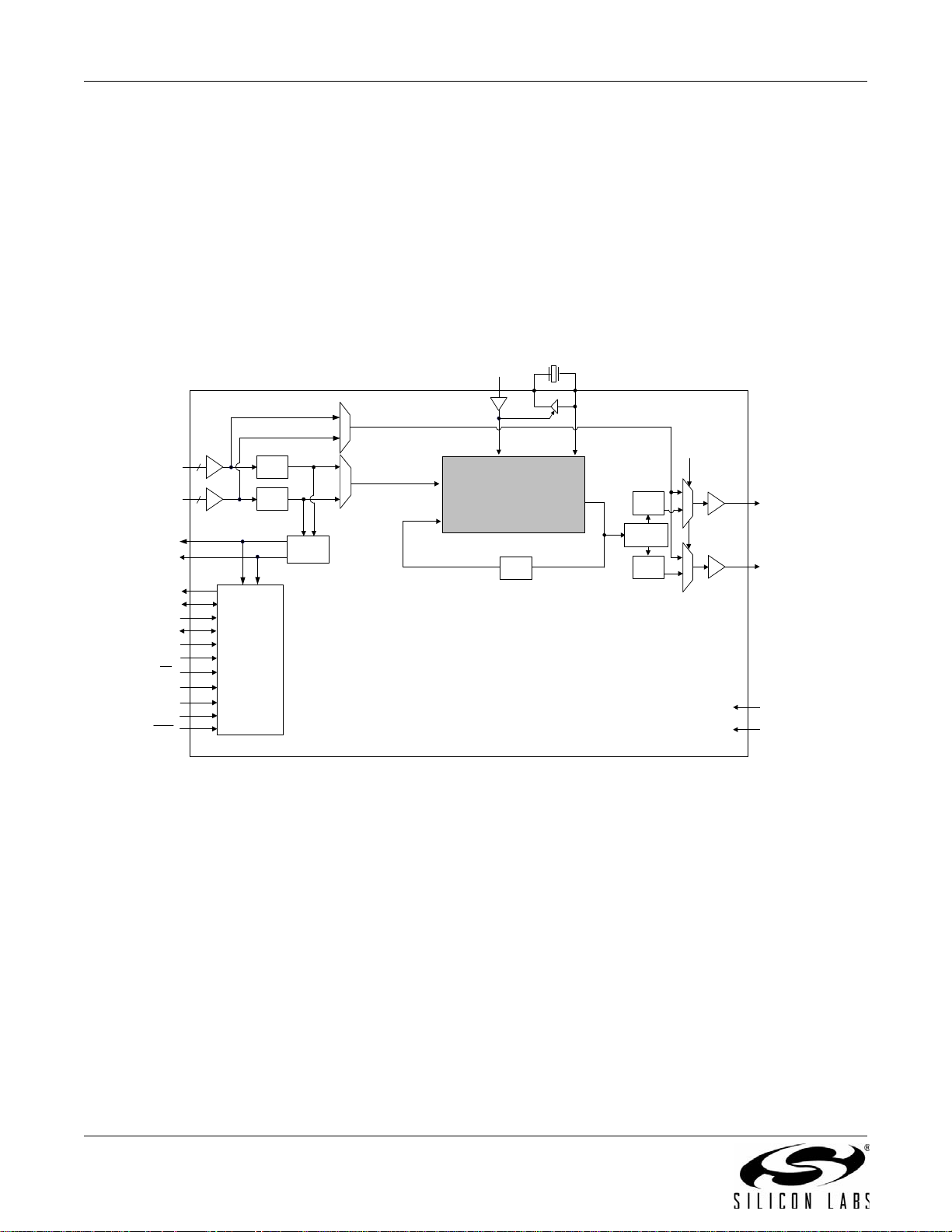
The Si5322 is a low jitter, precision clock multiplier for applications requiring clock multiplication without jitter
attenuation. The Si5322 acce pts dual clock inputs ranging from 19.44 to 707 MHz and generates two frequencymultiplied clock outputs ranging from 19.44 to 1050 MHz. The input clock frequency and clock multiplication ratio
are selectable from a table of popular SONET, Ethernet, Fibre Channel, and broadcast video (HD SDI, 3G SDI)
rates. The DSPLL loop bandwidth is digitally selectable from 150 kHz to 1.3 MHz. Operating from a single 1.8, 2.5,
or 3.3 V supply, the Si5322 is ideal for providing low jitter clock multiplication in high performance timing
applications. See "5. Pin Control Parts (Si5316, Si5322, Si5323, Si5365, Si5366)" on page 37 for a complete
description.
Figure 3. Si5322 Low Jitter Clock Multiplier Block Diagram
Note: Not recommended for new designs. For alternatives, see the Si533x family of products.
18 Rev. 1.2
Page 19
Si53xx-RM
DSPLL
®
C1B
LOL
CS/CA
BWSEL[1:0]
DBL2/BY
Xtal or R e fc lo ck
SFOUT[1:0]
CKOUT_2+
CKOUT_2–
CKIN_1+
CKIN_1–
CKOUT_1+
CKOUT_1–
CKIN_2+
CKIN_2–
Control
AUTOSEL
FRQTBL
Signal
Detect
VDD
GND
Frequency
Control
Bandwidth
Control
C2B
2
2
FRQSEL[3:0]
INC
DEC
RST
0
1
RATE[1:0]
XA
XB
f
OSC
2
2
0
1
0
1
f
3
3.4. Si5323
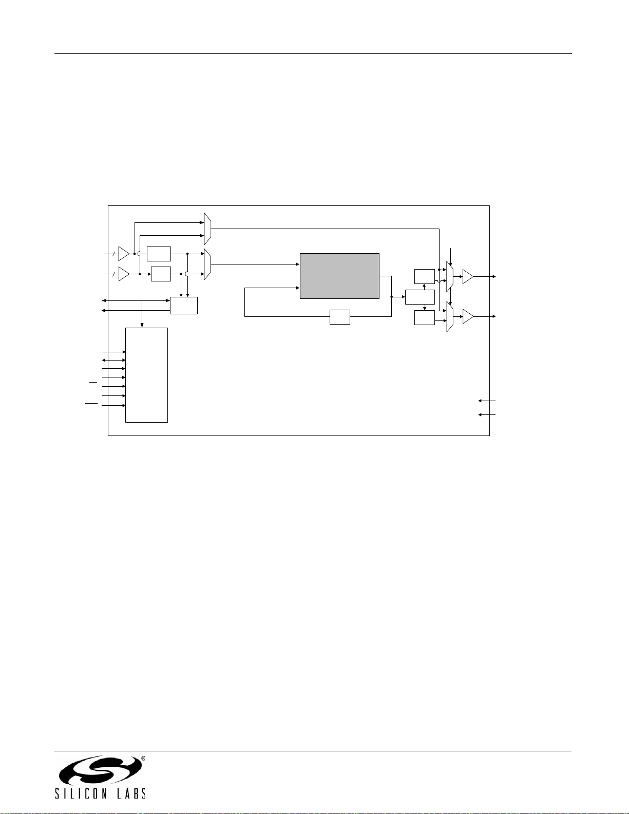
The Si5323 is a jitter-attenuating precision clock multiplier for high-speed communication systems, including
SONET OC-48/OC-192, Ethernet, Fibre Channel, and broadcast video (HD SDI, 3G SDI). The Si5323 accepts
dual clock inputs ranging from 8 kHz to 707 MHz and generates two frequency-multiplied clock outputs ranging
from 8 kHz to 1050 MHz. The input clock frequency and clock multiplication ratio are selectable from a table of
popular SONET, Ethernet, Fibre Channel, and broadcast video rates. The DSPLL loop bandwidth is digitally
selectable, providing jitter performance optimization at the application level. Operating from a single 1.8, 2.5, or
3.3 V supply, the Si5323 is ideal for providing clock multiplication and jitter attenuation in high-performance timing
applications. See "5. Pin Control Parts (Si5316, Si5322, Si5323, Si5365, Si5366)" on page 37 for a complete
description.
Rev. 1.2 19
Figure 4. Si5323 Jitter Attenuating Clock Multiplier Block Diagram
Page 20
Si53xx-RM
÷ N31
INT_C1B
Xtal or Re fc lo c k
÷ NC1
÷ NC2
Signal
Detect
VDD
GND
C2B
0
1
f
3
CKOUT_2 +
CKOUT_2 –
CKOUT_1 +
CKOUT_1 –
/
/
2
2
1
0
1
0
f
OSC
RATE[1:0 ]
LOL
CS_CA
SDA_SDO
INC
DEC
RST
SCL
Control
SDI
A[2]/SS
A[1:0]
XAXB
CMODE
CKIN_ 1 +
CKIN_ 1 –
2
2
CKIN_ 2 +
CKIN_ 2 –
÷ N32
0
1
3
BYPASS
÷ N2
DSPLL
÷ N1_HS
DSPLL
®
3.5. Si5324
The Si5324 is a jitter-attenuating precision clock multiplier for applications requiring sub 1 ps jitter performance.
The Si5324 accepts dual clock inputs ranging from 2 kHz to 710 MHz and generates two independent,
synchronous clock outputs ranging from 2 kHz to 945 MHz and select frequencies to 1.4 GHz. The device provides
virtually any frequency translation combination across this operating range. The Si5324 input clock frequency and
clock multiplication ratios are programmable th rough an I
programmable, providing jitter performance optimization at the application level. The Si5324 features loop
bandwidth values as low as 4 Hz. Operating from a single 1.8, 2.5, or 3.3 V supply, the Si5324 is ideal for providing
clock multiplication and jitter attenuation in high-performance timing applications. See "6. Microprocessor
Controlled Parts (Si5319, Si5324, Si5325, Si5326, Si5327, Si5328, Si5367, Si5368, Si5369, Si5374, Si5375, and
Si5376)" on page 63 for a complete description.
2
C or SPI interface. The DSPLL loop bandwid th is digit ally
Figure 5. Si5324 Clock Multiplier and Jitter Attenuator Block Diagram
20 Rev. 1.2
Page 21
Si53xx-RM
÷ N31
INT_C1B
÷ NC1
÷ NC2
Signal
Detect
C2B
0
1
CKOUT_2 +
CKOUT_2 –
CKOUT_1 +
CKOUT_1 –
/
/
2
2
1
0
1
0
SDA_SDO
RST
SCL
Control
SDI
A[2]/SS
A[1:0]
CMODE
CKIN_1 +
CKIN_1 –
2
2
CKIN_2 +
CKIN_2 –
÷ N32
0
1
BYPASS
÷ N2
f
3
DSPLL
®
VDD
GND
÷ N1_HS
f
OSC
3.6. Si5325
The Si5325 is a low jitter, precision clock multiplier for applications requiring clock multiplication without jitter
attenuation. The Si5325 accepts dual clock inputs ranging from 10 to 710 MHz and generates two independent,
synchronous clock outputs ranging from 2 kHz to 945 MHz and select frequencies to 1.4 GHz. The Si5325 input
clock frequency and clock multiplication ratios are programmable through an I
bandwidth is digitally program mable from 150 kHz to 1.3 MHz. Operating from a single 1.8, 2.5, or 3.3 V supply, the
Si5325 is ideal for providing clock multiplication in high performance timing applications. See "6. Microprocessor
Controlled Parts (Si5319, Si5324, Si5325, Si5326, Si5327, Si5328, Si5367, Si5368, Si5369, Si5374, Si5375, and
Si5376)" on page 63 for a complete description.
2
C or SPI interface. The DSPLL loop
Figure 6. Si5325 Low Jitter Clock Multiplier Block Diagram
Note: Not recommended for new designs. For alternatives, see the Si533x family of products.
Rev. 1.2 21
Page 22
Si53xx-RM
÷ N31
INT_C1B
Xtal or Re fc lo c k
÷ NC1
÷ NC2
Signal
Detect
VDD
GND
C2B
0
1
f
3
CKOUT_2 +
CKOUT_2 –
CKOUT_1 +
CKOUT_1 –
/
/
2
2
1
0
1
0
f
OSC
RATE[1:0]
LOL
CS_CA
SDA_SDO
INC
DEC
RST
SCL
Control
SDI
A[2]/SS
A[1:0]
XAXB
CMODE
CKIN_ 1 +
CKIN_ 1 –
2
2
CKIN_ 2 +
CKIN_ 2 –
÷ N32
0
1
3
BYPASS
÷ N2
DSPLL
÷ N1_HS
DSPLL
®
3.7. Si5326
The Si5326 is a jitter-attenuating precision clock multiplier for applications requiring sub 1 ps jitter performance.
The Si5326 accepts dual clock inputs ranging from 2 kHz to 710 MHz and generates two independent,
synchronous clock outputs ranging from 2 kHz to 945 MHz and select frequencies to 1.4 GHz. The device provides
virtually any frequency translation combination across this operating range. The Si5326 input clock frequency and
clock multiplication ratios are programmable th rough an I
programmable from 60 Hz to 8 kHz, providing jitter performance optimization at the application level. Operating
from a single 1.8, 2.5, or 3.3 V supply, the Si5326 is ideal for providing clock multiplication and jitter atte nuation in
high-performance timing applications. See "6. Microprocessor Controlled Parts (Si5319, Si5324, Si5325, Si5326,
Si5327, Si5328, Si5367, Si5368, Si5369, Si5374, Si5375, and Si5376)" on page 63 for a complete description.
2
C or SPI interface. The DSPLL loop bandwid th is digit ally
Figure 7. Si5326 Clock Multiplier and Jitter Attenuator Block Diagram
22 Rev. 1.2
Page 23
Si53xx-RM
÷ N31
INT_C1B
Xtal or Re fc lo c k
÷ NC1
÷ NC2
Signal
Detect
VDD
GND
C2B
0
1
f
3
CKOUT_2 +
CKOUT_2 –
CKOUT_1 +
CKOUT_1 –
/
/
2
2
1
0
1
0
f
OSC
RATE[1:0 ]
LOL
CS
SDA_SDO
RST
SCL
Control
SDI
A[2]/SS
A[1:0]
XAXB
CMODE
CKIN_ 1 +
CKIN_ 1 –
2
2
CKIN_ 2 +
CKIN_ 2 –
÷ N32
0
1
3
BYPASS
÷ N2
DSPLL
÷ N1_HS
DSPLL
®
3.8. Si5327
The Si5327 is a jitter-attenuating precision clock multiplier for applications requiring sub 1 ps jitter performance.
The Si5327 accepts dual clock inputs ranging from 2 kHz to 710 MHz and generates two independent,
synchronous clock outputs ranging from 2 kHz to 808 MHz. The device provides virtually any frequency translation
combination across this operating range. The Si5327 input clock frequency and clock multiplication ratios are
programmable through an I
jitter performance optimization at the application level. The Si5327 features loop bandwidth values as low as 4 Hz.
Operating from a single 1.8, 2. 5, or 3.3 V supply, the Si5327 is ideal for providing clock multiplication and jitter
attenuation in high-performance timing applications. See "6. Microprocessor Controlled Parts (Si5319, Si5324,
Si5325, Si5326, Si5327, Si5328, Si5367, Si5368, Si53 69, Si5374, Si5 375, a nd Si5376)" on page 63 for a complete
description.
2
C or SPI interface. The DSPLL loop bandwidth is digitally programmable, providing
Figure 8. Si5327 Clock Multiplier and Jitter Attenuator Block Diagram
Rev. 1.2 23
Page 24
Si53xx-RM
÷ N31
INT_C1B
÷ NC1
÷ NC2
Signal
Detect
VDD
GND
C2B
0
1
f
3
CKOUT_2 +
CKOUT_2 –
CKOUT_1 +
CKOUT_1 –
/
/
2
2
1
0
1
0
f
OSC
RATE[1:0]
CS_CA
RST
Control
XA
XB
CKIN_ 1 +
CKIN_ 1 –
2
2
CKIN_ 2 +
CKIN_ 2 –
÷ N32
0
1
3
BYPASS
÷ N2
DSPLL
÷ N1_HS
DSPLL
®
TCXO or Refclock
A[1:0]
A[2]/SS
SDI
SCL
SDA_SDO
CMODE
LOL
3.9. Si5328
The Si5328 is a jitter-attenuating precision clock multiplier for applications requiring sub-1 ps jitter performance and
digitally-programmable ultra-low-loop BW ranging from 0.05 to 6 Hz. When combined with a low-wander, low-jitter
reference oscillator, the Si5328 meets all of the wander, MTIE, TDEV, and other requirements that are listed in ITUT G.8262. The Si5328 accepts two input clocks ranging from 8 kHz to 346 MHz and generates two output clocks
ranging from 2 kHz to 346 MHz. The device provides virtually any frequency translation combination across the
operating range. The Si5328 input clock frequency and clock multiplication ratio are programmable through and
2
C or SPI interface. Operating from a single 1.8, 2.5, or 3.3 V supply, the Si5328 is ideal for providing multiplication
I
and jitter/wander attenuation in high-performance timing applications like SyncE timing cards. See "6.
Microprocessor Controlled Parts (Si5319, Si5324, Si5325, Si5326, Si5327, Si5328, Si5367, Si5368, Si5369,
Si5374, Si5375, and Si5376)" on page 63 for a complete description. Also see “AN775: Si5328 ITU-T G.8261
SyncE Compliance Test Report" and “AN776: Using the Si5328 in a G.8262 Compliant SyncE Application".
Figure 9. Si5328 Clock Multiplier and Jitter Attenuator Block Diagram
24 Rev. 1.2
Page 25
Si53xx-RM
C2A
CS0_C3A
C2B
CS1_C4A
ALRMOUT
C1A
CKIN_1+
CKIN_1–
CKIN_2+
CKIN_2–
C3B
CKIN_3+
CKIN_3–
CKIN_4+
CKIN_4–
C1B
VDD
GND
CKOUT_1+
CKOUT_1–
÷ NC1
1
0
CKOUT_2+
CKOUT_2–
÷ NC2
1
0
CKOUT_3+
CKOUT_3–
÷ NC3
1
0
CKOUT_4+
CKOUT_4–
÷ NC4
1
0
2
2
2
2
2
2
2
2
f
OSC
f
3
DBL2_BY
DBL34
DBL5
BWSEL[1:0]
FRQSEL[3:0]
DIV34[1:0]
FOS_CTL
SFOUT[1:0]
RST
CMODE
AUTOSEL
BYPASS/
DSBL2
Control
÷ N3_2
÷ N3_1
÷ N3_3
÷ N3_4
CKOUT_5+
CKOUT_5–
÷ NC5
1
0
2
FRQTBL
DIV34[1:0]
÷ N1_HS
DSPLL
®
÷ N2
3.10. Si5365
The Si5365 is a low jitter, precision clock multiplier for applications requiring clock multiplication without jitter
attenuation. The Si5365 accepts four clock inputs ranging from 19.44 MHz to 707 MHz and generates five
frequency-multiplied clock outputs ranging from 19.44 MHz to 1050 MHz. The input clock frequency and clock
multiplication ratio are selectable from a table of popular SONET, Ethernet, Fibre Channel, and broadcast video
rates. The DSPLL loop bandwidth is digitally selectable. Operating from a single 1.8, 2.5 V, or 3.3 V supply, the
Si5365 is ideal for providing clock multiplication in high performance timing applications. See "5. Pin Control Parts
(Si5316, Si5322, Si5323, Si5365, Si5366)" on page 37 for a complete descr iption.
Figure 10. Si5365 Low Jitter Clock Multiplier Block Diagram
Rev. 1.2 25
Note: Not recommended for new designs. For alternatives, see the Si533x family of products.
Page 26
Si53xx-RM
C2A
CS0_C3A
C2B
CS1_C4A
ALRMOUT
C1A
CKIN_1+
CKIN_1–
CKIN_2+
CKIN_2–
C3B
CKIN_3+
CKIN_3–
CKIN_4+
CKIN_4–
C1B
CKIN_3
CKIN_4
CKOUT_2
VDD
GND
CKOUT_1+
CKOUT_1–
÷ NC1
1
0
CKOUT_2+
CKOUT_2–
÷ NC2
1
0
CKOUT_3+
CKOUT_3–
÷ NC3
1
0
CKOUT_4+
CKOUT_4–
÷ NC4
1
0
2
2
2
2
2
2
2
2
f
OSC
Xtal or Refclock
RATE[1:0]
XA
XB
f
x
f
3
DBL2_BY
DBL34
DBL5
FSYNC
LOGIC/
ALIGN
CK_CONF
BWSEL[1:0]
FRQSEL[3:0]
DIV34[1:0]
FOS_CTL
SFOUT[1:0]
INC
DEC
FS_SW
FS_ALIGN
RST
CMODE
AUTOSEL
BYPASS/DSBL2
LOL
Control
÷ N3_2
÷ N3_1
FSYNC
3
÷ N3_3
÷ N3_4
CKOUT_5+
CKOUT_5–
÷ NC5
1
0
2
1
0
FRQTBL
DIV34[1:0]
÷ N1_HS
DSPLL
®
÷ N2
3.11. Si5366
The Si5366 is a jitter-attenuating precision clock multiplier for high-speed communication systems, including
SONET OC-48/OC-192, Etherne t, and Fibr e Chan nel. T he S i53 66 acce pts four clo ck inp uts ranging fr om 8 kHz to
707 MHz and generates five frequency-multiplied clock outputs ranging from 8 kHz to 1050 MHz. The input clock
frequency and clock multiplication ratio are selectable from a table of popular SONET, Ethernet, Fibre Channel,
and broadcast video (HD SDI, 3G SDI) rates. The DSPLL loop bandwidth is digitally selectable from 60 Hz to
8 kHz, providing jitter performance optimization at the application level. Operating from a single 1.8, 2.5, or 3.3 V
supply, the Si5366 is ideal for providing clock multiplication and jitter attenuation in high performance timing
applications. See "5. Pin Control Parts (Si5316, Si5322, Si5323, Si5365, Si5366)" on page 37 for a complete
description.
26 Rev. 1.2
Figure 11. Si5366 Jitter Attenuating Clock Multiplier Block Diagram
Page 27
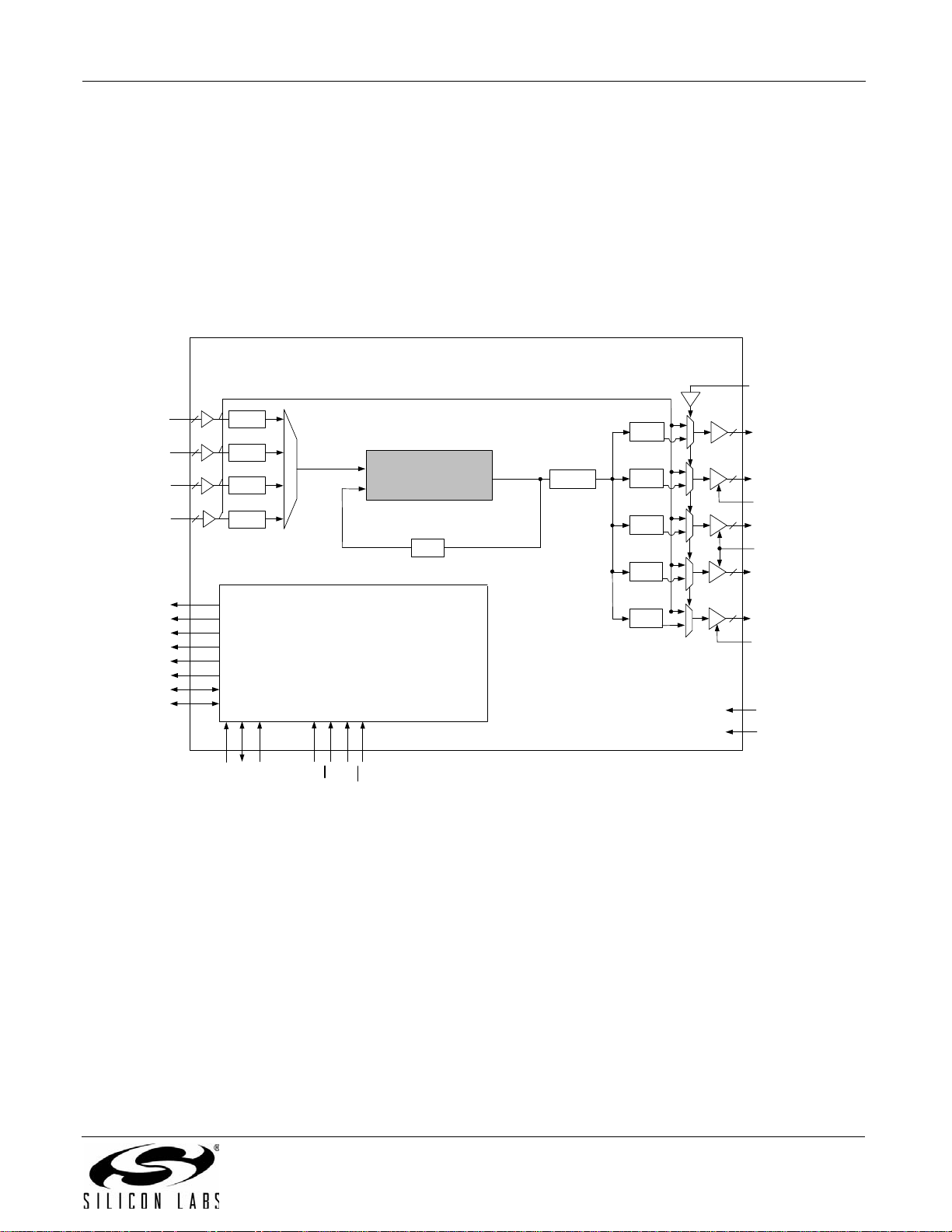
Si53xx-RM
C2A
CS0_C3A
C2B
CS1_C4A
INT_ALM
C1A
CKIN_1+
CKIN_1–
CKIN_2+
CKIN_2–
C3B
CKIN_3+
CKIN_3–
CKIN_4+
CKIN_4–
C1B
VDD
GND
CKOUT_1+
CKOUT_1–
÷ NC1
1
0
CKOUT_2+
CKOUT_2–
÷ NC2
1
0
CKOUT_3+
CKOUT_3–
÷ NC3
1
0
CKOUT_4+
CKOUT_4–
÷ NC4
1
0
2
2
2
2
2
2
2
2
f
OSC
f
3
DSBL2/BYPASS
DSBL34
DSBL5
SDA_SDO
SCL
SDI
A[1:0]
RST
CMODE
BYPASS/DSBL2
Control
÷ N3_2
÷ N3_1
÷ N2
3
÷ N3_3
÷ N3_4
CKOUT_5+
CKOUT_5–
÷ NC5
1
0
2
A[2]/SS
÷ N1_HS
DSPLL
®
3.12. Si5367
The Si5367 is a low jitter, precision clock multiplier for applications requiring clock multiplication without jitter
attenuation. The Si5367 accepts four clock inputs ranging from 10 to 707 MHz and generates five frequencymultiplied clock outputs ranging from 2 kHz to 945 MHz and select frequencies to 1.4 GHz. The Si5367 input clock
frequency and clock multiplication ratio are programmable through an I
bandwidth is digitally program mable from 150 kHz to 1.3 MHz. Operating from a single 1.8, 2.5, or 3.3 V supply, the
Si5367 is ideal for providing clock multiplication in high performance timing applications. See "6. Microprocessor
Controlled Parts (Si5319, Si5324, Si5325, Si5326, Si5327, Si5328, Si5367, Si5368, Si5369, Si5374, Si5375, and
Si5376)" on page 63 for a complete description.
2
C or SPI interface. The DSPLL loop
Note: Not recommended for new designs. For alternatives, see the Si53xx family of products.
Figure 12. Si5367 Clock Multiplier Block Diagram
Rev. 1.2 27
Page 28
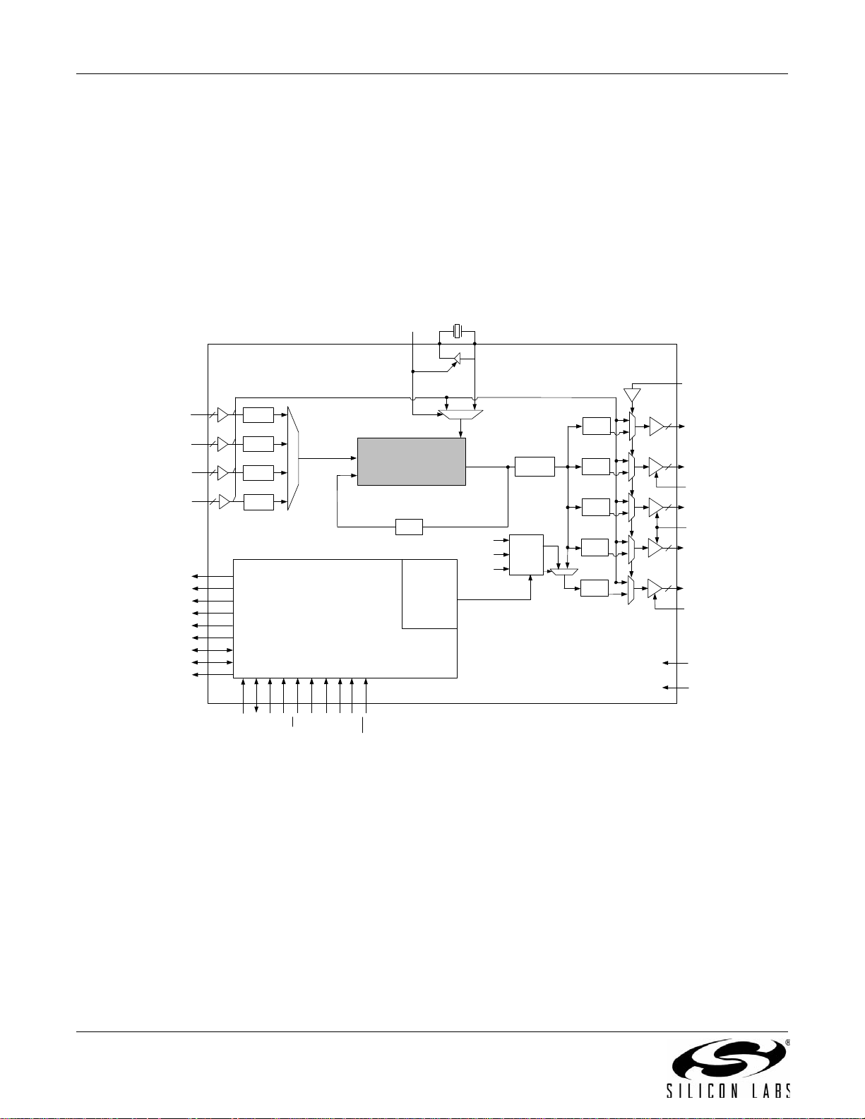
Si53xx-RM
C2A
CS0_C3A
C2B
CS1_C4A
INT_ALM
C1A
CKIN_1+
CKIN_1–
CKIN_2+
CKIN_2–
C3B
CKIN_3+
CKIN_3–
CKIN_4+
CKIN_4–
C1B
CKIN_3
CKIN_4
CKOUT_2
VDD
GND
CKOUT_1+
CKOUT_1–
÷ NC1
1
0
CKOUT_2+
CKOUT_2–
÷ NC2
1
0
CKOUT_3+
CKOUT_3–
÷ NC3
1
0
CKOUT_4+
CKOUT_4–
÷ NC4
1
0
2
2
2
2
2
2
2
2
f
OSC
Xtal or Refc lock
RATE[1:0]
XA
XB
f
x
DSBL2/BYPASS
DSBL34
DSBL5
FSYNC
LOGIC/
ALIGN
SDA_SDO
SCL
SDI
A[1:0]
INC
DEC
FS_ALIGN
RST
CMODE
BYPASS/DSBL2
LOL
Control
÷ N3_2
÷ N3_1
FSYNC
÷ N2
÷ N3_3
÷ N3_4
CKOUT_5+
CKOUT_5–
÷ NC5
1
0
2
1
0
A[2]/SS
÷ N1_HS
DSPLL
®
f
3
3
3.13. Si5368
The Si5368 is a jitter-attenuating precision clock multiplier for applications requiring sub 1 ps rms jitter
performance. The Si5368 accepts four clock inputs ranging from 2 kHz to 710 MHz and generates five
independent, synchronous clock outputs ranging from 2 kHz to 945 MHz and select frequencies to 1.4 GHz. The
device provides virtually any frequency translation combination across this operating range. The Si5368 input clock
frequency and clock multiplication ratio are programmable through an I
bandwidth is digitally programmable from 60 Hz to 8 kHz, providing jitter performance optimization at the
application level. Operating from a single 1.8, 2.5, or 3.3 V supply, the Si5368 is ideal for providing clock
multiplication and jitter attenuation in high performance timing applications. See "6. Microprocessor Controlled
Parts (Si5319, Si5324, Si5325, Si5326, Si5327, Si5328, Si5367, Si5368, Si5369, Si5374, Si5375, and Si5376)" on
page 63 for a complete description.
2
C or SPI interface. The DSPLL loop
Figure 13. Si5368 Clock Multiplier and Jitter Attenuator Block Diagram
28 Rev. 1.2
Page 29
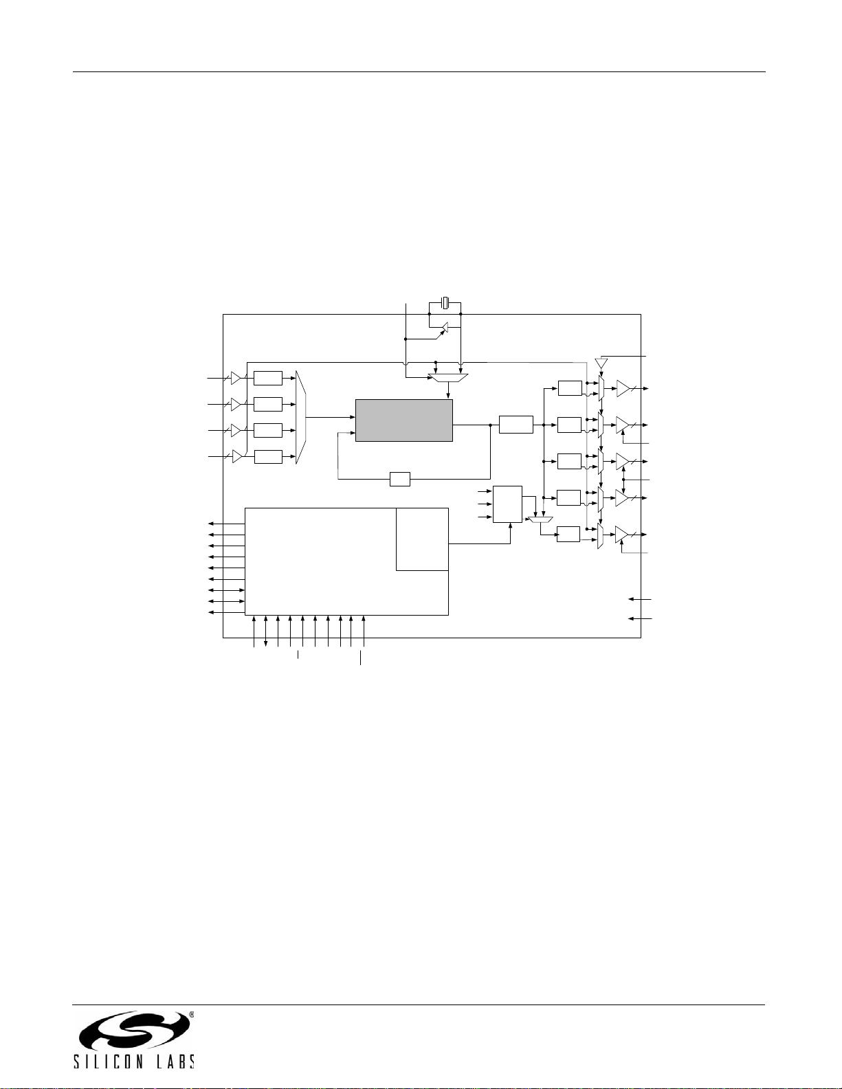
Si53xx-RM
C2A
CS0_C3A
C2B
CS1_C4A
INT_ALM
C1A
CKIN_1+
CKIN_1–
CKIN_2+
CKIN_2–
C3B
CKIN_3+
CKIN_3–
CKIN_4+
CKIN_4–
C1B
CKIN_3
CKIN_4
CKOUT_2
VDD
GND
CKOUT_1+
CKOUT_1–
÷ NC1
1
0
CKOUT_2+
CKOUT_2–
÷ NC2
1
0
CKOUT_3+
CKOUT_3–
÷ NC3
1
0
CKOUT_4+
CKOUT_4–
÷ NC4
1
0
2
2
2
2
2
2
2
2
f
OSC
Xtal or Refclock
RATE[1:0]
XA
XB
f
x
DSBL2/BYPASS
DSBL34
DSBL5
FSYNC
LOGIC/
ALIGN
SDA_SDO
SCL
SDI
A[1:0]
INC
DEC
FS_ALIGN
RST
CMODE
BYPASS/DSBL2
LOL
Control
÷ N3_2
÷ N3_1
FSYNC
÷ N2
÷ N3_3
÷ N3_4
CKOUT_5+
CKOUT_5–
÷ NC5
1
0
2
1
0
A[2]/SS
÷ N1_HS
DSPLL
®
f
3
3
3.14. Si5369
The Si5369 is a jitter-attenuating precision clock multiplier for applications requiring sub 1 ps rms jitter
performance. The Si5369 accepts four clock inputs ranging from 2 kHz to 710 MHz and generates five
independent, synchronous clock outputs ranging from 2 kHz to 945 MHz and select frequencies to 1.4 GHz. The
device provides virtually any frequency translation combination across this operating range. The Si5369 input clock
frequency and clock multiplication ratio are programmable through an I
bandwidth is digitally programmable, providing loop bandwidth values as low as 4 Hz. Operating from a single 1.8,
2.5, or 3.3 V supply, the Si5369 is ideal for providing clock multiplication and jitter attenuation in high performance
timing applications. See "6. Microprocessor Controlled Parts (Si5319, Si5324, Si5325, Si5326, Si5327, Si5328,
Si5367, Si5368, Si5369, Si5374, Si5375, and Si5376)" on page 63 for a complete description.
2
C or SPI interface. The DSPLL loop
Figure 14. Si5369 Clock Multiplier and Jitter Attenuator Block Diagram
3.15. Si5374/75/76 Compared to Si5324/19/26
In general, the Si5374 can be viewed as a quad version of the Si5324, and the Si5375 can be viewed as a quad
version of the Si5319, and the Si5376 can be viewed as a quad version of the Si5326. However, they are not
exactly the same. This is an overview of the differences:
1. The Si5374/75/76 cannot use a crystal as its OSC reference. It requires the use of a single external singleended or differential crystal oscillator.
2. The Si5374/75/76 only supports I
available on the Si5374/75/76.
3. The Si5374/75/76 does not provide separate INT_CK1B and CK2B pins to indicate when CKIN1 and CKIN2 do
not have valid clock inputs. Instead, the IRQ pin can be programmed to function as one pin, the other pin or
both.
4. Selection of the OSC frequency is done by a register (RATE_REG), not by using the RATE pins.
5. The Si5374/75/76 uses a different version of DSPLLsim: Si537xDSPLLsim.
6. The Si5374/75/76 does not support 3.3 V operation.
2
C as its serial port protocol and does not have SPI. No I2C address pins are
Rev. 1.2 29
Page 30
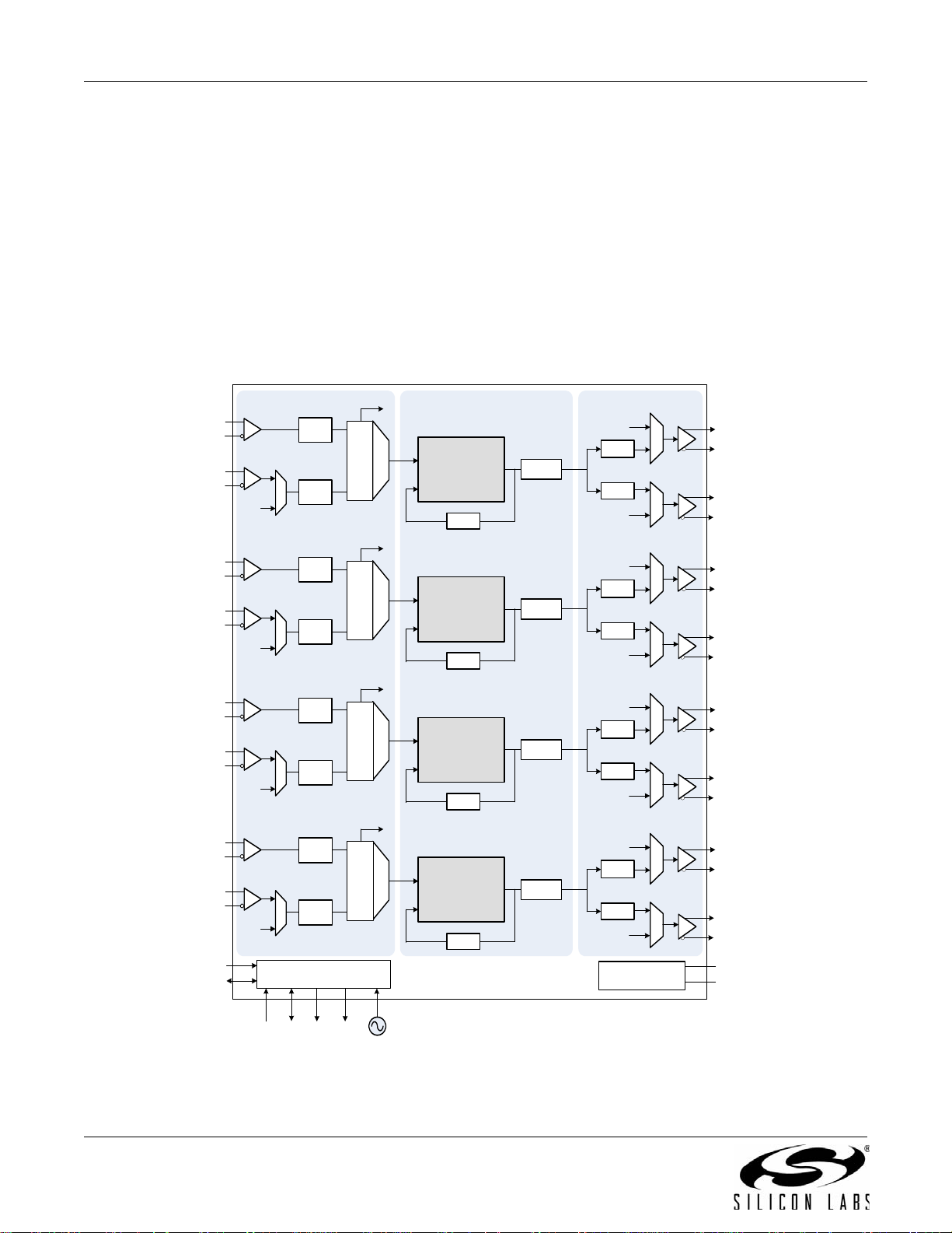
Si53xx-RM
CKIN3P_B
CKOUT3N_B
÷ N31
DSPLL
®
B
÷ NC1
÷ NC2
CKIN3N_B
CKIN4P_B
÷ N32
CKIN4N_B
Internal
Osc
PLL Bypass
CKOUT3P_B
CKOUT4N_B
CKOUT4P_B
f
OSC
÷ NC1_HS
Input
Monitor
Hitless
Switch
PLL Bypass
f
3
÷ N2
Status / Control
PLL Bypass
High PSRR
Voltage Regulator
VDD_q
GND
Synthesis Stage
CKIN1P_A
CKOUT1N_A
÷ N31
DSPLL
®
A
÷ NC1
÷ NC2
CKIN1N_A
CKIN2P_A
÷ N32
CKIN2N_A
Internal
Osc
PLL Bypass
CKOUT1P_A
CKOUT2N_A
CKOUT2P_A
Output Stage
f
OSC
÷ NC1_HS
Input
Monitor
Hitless
Switch
PLL Bypass
f
3
÷ N2
PLL Bypass
Input Stage
CKIN7P_D
CKOUT7N_D
÷ N31
DSPLL
®
D
÷ NC1
÷ NC2
CKIN7N_D
CKIN8P_D
÷ N32
CKIN8N_D
Internal
Osc
PLL Bypass
CKOUT7P_D
CKOUT8N_D
CKOUT8P_D
f
OSC
÷ NC1_HS
Input
Monitor
Hitless
Switch
PLL Bypass
f
3
÷ N2
PLL Bypass
CKIN5P_C
CKOUT5N_C
÷ N31
DSPLL
®
C
÷ NC1
÷ NC2
CKIN5N_C
CKIN6P_C
÷ N32
CKIN6N_C
Internal
Osc
PLL Bypass
CKOUT5P_C
CKOUT6N_C
CKOUT6P_C
f
OSC
÷ NC1_HS
Input
Monitor
Hitless
Switch
PLL Bypass
f
3
÷ N2
PLL Bypass
RSTL_q
CS_q
SCL SDA
LOL_q
IRQ_q
Low Jitter
XO or Clock
OSC_P/N
3.16. Si5374
The Si5374 is a highly integrated , 4- PLL jit ter- atten uat ing precision clock multiplier for applications requiring sub 1
ps jitter performance. Each of the DSPLL® clock multiplier engines accepts two input clocks ranging from 2 kHz to
710 MHz and generates two independent, synchronous output clocks ranging from 2 kHz to 808 MHz. Each
DSPLL provides virtually any frequency translation across this operating range. For asynchronous, free-running
clock generation applications, the Si5374’s reference oscillator can be used as a clock source for the four DSPLLs.
The Si5374 input clock frequency and clock multiplication ratio are programmable through an I2C interface. The
Si5374 is based on Silicon Laboratories' 3rd-generation DSPLL® technology, which provides any-frequency
synthesis and jitter attenuation in a highly integrated PLL solution that eliminates the need for external VCXO and
loop filter components. Each DSPLL loop bandwidth is digitally programmable from 4 to 525 Hz, providing jitter
performance optimization at the application level. The device operates from a single 1.8 or 2.5 V supply with onchip voltage regulators with excellent PSRR. The Si5374 is ideal for providing clock multiplication and jitter
attenuation in high port count optical line cards requiring independent timing domains.
Figure 15. Si5374 Functional Block Diagram
30 Rev. 1.2
Page 31

Si53xx-RM
CKIN1P_B
÷ N31
DSPLL
®
B
CKIN1N_B
÷ N32
f
OSC
÷ NC1_HS
Input
Monitor
f
3
÷ N2
Status / Control
PLL Bypass
High PSRR
Voltage Regulator
VDD_q
GND
Synthesis Stage
CKIN1P_A
CKOUT1N_A
÷ N31
DSPLL
®
A
CKIN1N_A
÷ N32
CKOUT1P_A
Output Stage
f
OSC
÷ NC1_HS
Input
Monitor
f
3
÷ N2
PLL Bypass
Input Sta ge
CKIN1P_D
÷ N31
DSPLL
®
D
CKIN1N_D
÷ N32
f
OSC
÷ NC1_HS
Input
Monitor
f
3
÷ N2
PLL Bypass
CKIN1P_C
÷ N31
DSPLL
®
C
CKIN1N_C
÷ N32
f
OSC
÷ NC1_HS
Input
Monitor
f
3
÷ N2
PLL Bypass
RSTL_q
CS_q
SCL SDA
LOL_q
IRQ_q
Low Jitter
XO or Clock
OSC_P/N
÷ NC1
PLL Bypass
CKOUT1N_B
÷ NC1
PLL Bypass
CKOUT1P_B
CKOUT1N_C
PLL Bypass
CKOUT1P_C
÷ NC1
CKOUT1N_D
÷ NC1
PLL Bypass
CKOUT1P_D
3.17. Si5375
The Si5375 is a highly integrated , 4- PLL jit ter- atten uat ing precision clock multiplier for applications requiring sub 1
ps jitter performance. Each of the DSPLL® clock multiplier engines accepts an input clock ranging from 2 kHz to
710 MHz and generates an output clock ranging from 2 kHz to 808 MHz. Each DSPLL provides virtually any
frequency translation combination across this operating range. For asynchronous, free-running clock generation
applications, the Si5375’s reference oscillator can be used as a clock source for any of the four DSPLLs. The
Si5375 input clock frequency and clock multiplication ratio are programma ble through an I2C interface. The Si5375
is based on Silicon Laboratories' third-generation DSPLL® technology, which provides any-frequency synthesis
and jitter attenuation in a highly integrated PLL solution that eliminates the need for external VCXO and loop filter
components. Each DSPLL loop bandwidth is digitally programmable from 60 Hz to 8 kHz, providing jitter
performance optimization at the application level. The device operates from a single 1.8 or 2.5 V supply with onchip voltage regulators with excellent PSRR. The Si5375 is ideal for providing clock multiplication and jitter
attenuation in high port count optical line cards requiring independent timing domains.
Figure 16. Si5375 Functional Block Diagram
Rev. 1.2 31
Page 32

Si53xx-RM
CKIN3P_B
CKOUT3N_B
÷ N31
DSPLL
®
B
÷ NC1
÷ NC2
CKIN3N_B
CKIN4P_B
÷ N32
CKIN4N_B
Internal
Osc
PLL Bypass
CKOUT3P_B
CKOUT4N_B
CKOUT4P_B
f
OSC
÷ NC1_HS
Input
Monitor
Hitless
Switch
PLL Bypass
f
3
÷ N2
Status / Control
PLL Bypass
High PSRR
Voltage Regulator
VDD_q
GND
Synthesis Stage
CKIN1P_A
CKOUT1N_A
÷ N31
DSPLL
®
A
÷ NC1
÷ NC2
CKIN1N_A
CKIN2P_A
÷ N32
CKIN2N_A
Internal
Osc
PLL Bypass
CKOUT1P_A
CKOUT2N_A
CKOUT2P_A
Output Stage
f
OSC
÷ NC1_HS
Input
Monitor
Hitless
Switch
PLL Bypass
f
3
÷ N2
PLL Bypass
Input Stage
CKIN7P_D
CKOUT7N_D
÷ N31
DSPLL
®
D
÷ NC1
÷ NC2
CKIN7N_D
CKIN8P_D
÷ N32
CKIN8N_D
Internal
Osc
PLL Bypass
CKOUT7P_D
CKOUT8N_D
CKOUT8P_D
f
OSC
÷ NC1_HS
Input
Monitor
Hitless
Switch
PLL Bypass
f
3
÷ N2
PLL Bypass
CKIN5P_C
CKOUT5N_C
÷ N31
DSPLL
®
C
÷ NC1
÷ NC2
CKIN5N_C
CKIN6P_C
÷ N32
CKIN6N_C
Internal
Osc
PLL Bypass
CKOUT5P_C
CKOUT6N_C
CKOUT6P_C
f
OSC
÷ NC1_HS
Input
Monitor
Hitless
Switch
PLL Bypass
f
3
÷ N2
PLL Bypass
RSTL_q
CS_q
SCL SDA
LOL_q
IRQ_q
Low Jitter
XO or Clock
OSC_P/N
3.18. Si5376
The Si5376 is a highly integrated , 4- PLL jit ter- atten uat ing precision clock multiplier for applications requiring sub 1
ps jitter performance. Each of the DSPLL® clock multiplier engines accepts two input clocks ranging from 2 kHz to
710 MHz and generates two independent, synchronous output clocks ranging from 2 kHz to 808 MHz. Each
DSPLL provides virtually any frequency translation across this operating range. For asynchronous, free-running
clock generation applications, the Si5376’s reference oscillator can be used as a clock source for the four DSPLLs.
The Si5376 input clock frequency and clock multiplication ratio are programmable through an I
Si5376 is based on Silicon Laboratories' 3rd-generation DSPLL® technology, which provides any-frequency
synthesis and jitter attenuation in a highly integrated PLL solution that eliminates the need for external VCXO and
loop filter components. Each DSPLL loop bandwidth is digitally programmable from 60 Hz to 8 kHz, providing jitter
performance optimization at the application level. The device operates from a single 1.8 or 2.5 V supply with onchip voltage regulators with excellent PSRR. The Si5376 is ideal for providing clock multiplication and jitter
attenuation in high port count optical line cards requiring independent timing domains.
2
C interface. The
Figure 17. Si5376 Functional Block Diagram
32 Rev. 1.2
Page 33

Si53xx-RM
f
IN
DSPLL
Phase
Detector
Digital
DCO
Digital Loop
Filter
Fvco
M
f
OUT
4. DSPLL (All Devices)
All members of the Any-Frequency Precision Clocks family incorporate a phase-locked loop (PLL) that utilizes
Silicon Laboratories' third generation DSPLL technology to eliminate jitter, noise, and the need for external VCXO
and loop filter components found in discrete PLL implementations. This is achieved by using a digital signal
processing (DSP) algorithm to replac e the loop filter commonly found in discrete PLL designs. Because external
PLL components are not required, sensitivity to board-level noise sources is minimized. This digital technology
provides highly stable and consistent operation over process, temperature, and voltage variations.
A simplified block diagram of the DSPLL is shown in Figure 18. This algorithm processes the phase detector error
term and generates a digital frequency control word M to adjust the frequency of the digitally-controlled oscillator
(DCO). The narrowband configuration devices (Si5316, Si5319, Si5323, Si5324, Si5326, Si5327, Si5366, Si5368,
and Si5369) provide ultra-low jitter generation by using an external jitter reference clock and jitter attenuation. For
applications where basic frequency multiplication of low jitter clocks is all that is required, the wideband parts
(Si5322, Si5325, Si5365, and Si5367) are available.
Figure 18. Any-Frequency Precision Clock DSPLL Block Diagram
Rev. 1.2 33
Page 34

Si53xx-RM
Fin
DSPLL
Phase
Detector
Digital
DCO
Digital Loop
Filter
Divide By N2
Divide By N3
Divide By NC1
Fout
f
OUT
= (Fin/N3) x N2/NC1
f
vco
= (Fin/N3) x N2
f
3
f
VCO
4.1. Clock Multiplication
Fundamental to these parts is a clock multiplication circuit th at is simplified in Figure 19. By having a large range of
dividers and multipliers, nearly any output frequency can be created from a fixed input frequency. For typical
telecommunications and data communications applications, the hardware control parts (Si5316, Si5322, Si5323,
Si5365, and Si5366) provide simple pin control.
The microprocessor controlled parts (Si5319, Si5324, Si5325, Si5326, Si5327, Si5367, Si5368, and Si5369)
provide a programmable range of clock multiplications. To assist users in finding valid divider settings for a
particular input frequency and clock multiplication ratio, Silicon Laboratories offers PC-based software (DSPLLsim)
that calculates these settings automatically. When multiple divider combinations produce the same output
frequency, the software recommends the divider settings yielding the recommended settings for phase noise
performance and power consumption.
Figure 19. Clock Multiplication Circuit
34 Rev. 1.2
Page 35

Si53xx-RM
Jitter
Transfer
0 dB
BW
f
Jitter
Peaking
–20 dB/dec.
Jitter Out
Jitter In
)
(
20 x LOG
4.2. PLL Performance
All members of the Any-Frequency Precision Clock family of devices provide extremely low jitter generation, a wellcontrolled jitter transfer function, and high jitter tolerance. For mor e information the loop bandwidth and its effect o n
jitter attenuation, see "Appendix H—Jitter Attenuation and Loop BW" on page 157.
4.2.1. Jitter Generation
Jitter generation is defined as the amount of jitter produced at the output of the device with a jitter free input clock.
Generated jitter arises from sources within the VCO and other PLL components. Jitter generation is a function of
the PLL bandwidth setting. Higher loop bandwidth settings may result in lower jitter generation, but may result in
less attenuation of jitter that might be present on the input clock signal.
4.2.2. Jitter Transfer
Jitter transfer is defined as the ratio of output signal jitter to input signal jitter for a specified jitter frequency. The
jitter transfer characteristic determines the amount of input clock jitter that passes to the outputs. The DSPLL
technology used in the Any-Frequency Precision Clock devices provides tightly controlled jitter transfer curves
because the PLL gain parameters are determined larg ely by digital circuits which do not vary over supply voltage,
process, and temperature. In a system application, a well-controlled transfer curve minim izes the output clock jitter
variation from board to board and provides more consistent system level jitter performance.
The jitter transfer characteristic is a function of the loop bandwidth setting. Lower bandwidth settings result in more
jitter attenuation of the incoming clock, but may result in higher jitter generation. Section 1 Any-Frequency
Precision Clock Product Family Overview also includes specifications related to jitter bandwidth and peaking.
Figure 20 shows the jitter transfer curve mask.
Figure 20. PLL Jitter Transfer Mask/Template
Rev. 1.2 35
Page 36

Si53xx-RM
Input
Jitter
Amplitude
A
j0
–20 dB/dec.
f
Jitter In
Excessive Input Jitter Range
BW/100 BW/10
BW
A
j0
5000
BW
------------ -
ns pk-pk=
A
j0
5000
100
------------ -
50 ns pk-pk==
4.2.3. Jitter Tolerance
Jitter tolerance is defined as the maximum peak-to-peak sinusoidal jitter that can be present on the incoming clock
before the DSPLL loses lock. The tolerance is a function of the jitter frequency, because tolerance improves for
lower input jitter frequency.
The jitter tolerance of the DSPLL is a function of the loop bandwidth setting. Figure 21 shows the general shape of
the jitter tolerance curve versus input jitter frequency. For jitter frequencies above the loop bandwidth, the tolerance
is a constant value A
lower input jitter frequencies.
. Beginning at the PLL bandwidth, the tolerance increases at a rate of 20 dB/decade for
j0
The equation for the high frequency jitter tolerance can be expressed as a function of the PLL loop bandwidth (i.e.,
bandwidth):
For example, the jitter tolerance when f
Figure 21. Jitter Tolerance Mask/Template
= 155.52 MHz, f
in
= 622.08 MHz and the loop bandwid th ( BW) is 100 Hz:
out
36 Rev. 1.2
Page 37

Si53xx-RM
5. Pin Control Parts (Si5316, Si5322, Si5323, Si5365, Si5366)
These parts provide high-performance clock multiplication with simple pin control. Many of the control inputs are
three levels: High, Low, and Medium. High and Low are standard voltage levels determined by the supply voltage:
and Ground. If the input pin is left floating, it is driven to nominally half of VDD. Effectively, this creates three
V
DD
logic levels for these controls.
These parts span a range of applications and I/O capacity as shown in Table 3.
Table 3. Si5316, Si5322, Si5323, Si5365 and Si5366 Key Features
Si5316 Si5322 Si5323 Si5365 Si5366
SONET Frequencies
DATACOM Frequencies
DATACOM/SONET internetworking
Fixed Ratio between input clocks
Flexible Frequency Plan
Number of Inputs 2 2 2 4 4
Number of Outputs 1 2 2 5 5
Jitter Attenuation
5.1. Clock Multiplication (Si5316, Si5322, Si5323, Si5365, Si5366)
By setting the tri-level FRQSEL[3:0] pins these devices provide a wide range of standard SONET and data
communications frequency scaling, including simple integer frequency multiplication to fractional settings required
for coding and decoding.
5.1.1. Clock Multiplication (Si5316 )
The device accepts dual input clocks in the 19, 39, 78, 155, 311, or 622 MHz frequency range and generates a dejittered output clock at the same frequency. The frequency range is set by the FRQSEL [1:0] pins, as shown in
Table 4.
Table 4. Frequency Settings
FRQSEL[1:0] Output Frequency (MHz)
LL 19.38–22.28
LM 38.75–44.56
LH 77.50–89.13
ML 155.00–178.25
MM 310.00–356.50
MH 620.00–710.00
Rev. 1.2 37
Page 38

Si53xx-RM
1, 4, 32
1, 4, 32
CKIN1
CKIN2
DSPLL
F
out
f3 = F
out
f
3
One-to-one
frequency ratio
The Si5316 can accept a CKIN1 input at a different frequency than the CKIN2 input. The frequency of one input
clock can be 1x, 4x, or 32x the frequency of the other inpu t clock. The o utput frequency is always equal to the lower
of the two clock inputs and is set via the FRQSEL [1:0] pins. The frequency applied at each clock input is divided
down by a pre-divider as shown in the Figure 1 on page 16. These pre-dividers must be set such that the two
resulting clock frequencies, f3_1 and f3_2 must be equal and are set by the FRQSEL [1:0] pins. Input divider
settings are controlled by the CK1DIV and CK2DIV pins, as shown in Table 5.
Table 5. Input Divider Settings
CKnDIV N3n Input Divider
L1
M4
H32
Table 6. Si5316 Bandwidth Values
FRQSEL[1:0] Nominal Frequency Values (MHz)
LL LM LH ML MM MH
BW[1:0] 19.44 MHz 38.88 MHz 77.76 MHz 155.52 MHz 311.04 MHz 622.08 MHz
HM 100 Hz 100 Hz 100 Hz 100 Hz 100 Hz 100 Hz
HL 210 Hz 210 Hz 200 Hz 200 Hz 200 Hz 200 Hz
MH 410 Hz 410 Hz 400 Hz 400 Hz 400 Hz 400 Hz
MM 1.7kHz 1.7kHz 1.6kHz 1.6kHz 1.6kHz 1.6kHz
ML 7.0kHz 7.0kHz 6.8kHz 6.7kHz 6.7kHz 6.7kHz
Figure 22. Si5316 Divisor Ratios
38 Rev. 1.2
Page 39

Si53xx-RM
5.1.2. Clock Multiplicatio n (Si5322, Si5323, Si5365, Si5366)
These parts provide flexible frequency plans for SONET, DATACOM, and interworking between the two (Table 7,
Table 8, an d Table 9 respectively). The CKINn inputs must be the same frequency as specified in the tables. The
outputs are the same frequency; however, in the Si5365 and Si5366, CKOUT3 and CKOUT4 can be further divided
down by using the DIV34 [1:0] pins.
The following notes apply to Tables 7, 8, and 9:
1. All entries are available for the Si5323 and Si5366. Only those marked entries under the WB column are
available for the Si5322 and Si5365.
2. The listed output frequencies appear on CKOUTn. For the Si5365 and Si5366, sub-multiples are available on
CKOUT3 and CKOUT4 using the DIV34[1:0] control pins.
3. All ratios are exact, but the frequ e ncy values ar e ro u nd ed .
4. For bandwidth settings, f3 values, and frequency operating ranges, consult DSPLLsim.
5. For the Si5366 with CK_CONF = 1, CKIN3 and CKIN4 are the same frequency as FS_OUT.
Table 7. SONET Clock Multiplication Settings (FRQTBL=L)
No FRQSEL
[3:0]
0 LLLL 0.008 1 0.008 0.008 0.008
1 LLLM 2430 19.44 19.44 0.008
2 LLLH 4860 38.88 38.88 0.008
3 LLML 9720 77.76 77.76 0.008
4 LLMM 19440 155.52 155.52 0.008
5 LLMH 38880 311.04 311.04 0.008
6 LLHL 77760 622.08 622.08 0.008
fIN MHz Mult Factor Nominal
WB
f
OUT
MHz
All Devices Si5366 Only
f
CKOUT5
(CK_CONF = 0)
(MHz)
FS_OUT (MHz)
(CK_CONF = 1)
Rev. 1.2 39
Page 40

Si53xx-RM
Table 7. SONET Clock Multiplication Settings (FRQTBL=L) (Continued)
No FRQSEL
[3:0]
7LLHM
8LLHH
9LMLL
10 LMLM
11 LMLH 8 x (255/238) 166.63 166.63 NA
12 LMML 8 x (255/237) 167.33 167.33 NA
13 LMMM 8 x (255/236) 168.04 168.04 NA
14 LMMH
15 LMHL
16 LMHM 32 x (255/238) 666.51 666.51 NA
17 LMHH 32 x (255/237) 669.33 669.33 NA
18 LHLL 32 x (255/236) 672.16 672.16 NA
19 LHLM
fIN MHz Mult Factor Nominal
WB
19.44 1 19.44 19.44 0.008
2 38.88 38.88 0.008
4 77.76 77.76 0.008
8 155.52 155.52 0.008
16 311.04 311.04 0.008
32 622.08 622.08 0.008
48 933.12 933.12 0.008
f
OUT
MHz
All Devices Si5366 Only
f
CKOUT5
(CK_CONF = 0)
(MHz)
FS_OUT (MHz)
(CK_CONF = 1)
20 LHLH
21 LHML
22 LHMM
23 LHMH
24 LHHL
25 LHHM 16 x (255/238) 666.51 666.51 NA
26 LHHH 16 x (255/237) 669.33 669.33 NA
27 MLLL 16 x (255/236) 672.16 672.16 NA
38.88 1 38.88 38.88 0.008
54 1049.76 1049.76 0.008
2 77.76 77.76 0.008
4 155.52 155.52 0.008
16 622.08 622.08 0.008
40 Rev. 1.2
Page 41

Si53xx-RM
Table 7. SONET Clock Multiplication Settings (FRQTBL=L) (Continued)
No FRQSEL
[3:0]
28 MLLM
29 MLLH
30 MLML
31 MLMM
32 MLMH
33 MLHL 2 x (255/237) 167.33 167.33 NA
34 MLHM 2 x (255/236) 168.04 168.04 NA
35 MLHH
36 MMLL
37 MMLM
38 MMLH 8 x (255/237) 669.33 669.33 NA
39 MMML 8 x (255/236) 672.16 672.16 NA
40 MMMM
fIN MHz Mult Factor Nominal
MHz
f
WB
77.76 1/4 19.44 19.44 0.008
1/2 38.88 38.88 0.008
1 77.76 77.76 0.008
2 155.52 155.52 0.008
2 x (255/238) 166.63 166.63 NA
4 311.04 311.04 0.008
8 622.08 622.08 0.008
8 x (255/238) 666.51 666.51 NA
155.52 1/8 19.44 19.44 0.008
OUT
All Devices Si5366 Only
f
CKOUT5
(CK_CONF = 0)
(MHz)
FS_OUT (MHz)
(CK_CONF = 1)
41 MMMH
42 MMHL
43 MMHM
44 MMHH
45 MHLL 255/237 167.33 167.33 NA
46 MHLM 255/236 168.04 168.04 NA
47 MHLH
48 MHML
49 MHMM
50 MHMH 4 x (255/237) 669.33 669.33 NA
51 MHHL 4 x (255/236) 672.16 672.16 NA
52 MHHM
53 MMHM
54 MHHH
55 MHML
166.63 238/255 155.52 155.52 NA
1/4 38.88 38.88 0.008
1/2 77.76 77.76 0.008
1 155.52 155.52 0.008
255/238 166.63 166.63 NA
2 311.04 311.04 0.008
4 622.08 622.08 0.008
4 x (255/238) 666.51 666.51 NA
1 166.63 166.63 NA
4 x (238/255) 622.08 622.08 NA
4 666.51 666.51 NA
Rev. 1.2 41
Page 42

Si53xx-RM
Table 7. SONET Clock Multiplication Settings (FRQTBL=L) (Continued)
No FRQSEL
[3:0]
56 HLLL 167.33 237/255 155.52 155.52 NA
57 MMHM
58 HLLM 4 x (237/255) 622.08 622.08 NA
59 MHML
60 HLLH 168.04 236/255 155.52 155.52 NA
61 MMHM
62 HLML 4 x (236/255) 622.08 622.08 NA
63 MHML
64 HLMM
65 HLMH
66 HLHL
67 HLHM 2 x (255/237) 669.33 669.33 NA
68 HLHH 2 x (255/236) 672.16 672.16 NA
fIN MHz Mult Factor Nominal
MHz
f
WB
311.04 1 311.04 311.04 0.008
1 167.33 167.33 NA
4 669.33 669.33 NA
1 168.04 168.04 NA
4 672.16 672.16 NA
2 622.08 622.08 0.008
2 x (255/238) 666.51 666.51 NA
OUT
All Devices Si5366 Only
f
CKOUT5
(CK_CONF = 0)
(MHz)
FS_OUT (MHz)
(CK_CONF = 1)
69 HMLL
70 HMLM
71 HMLH
72 HMML
73 HMMM
74 HMMH
75 HMHL
76 HMHM 255/237 669.33 669.33 NA
77 HMHH
78 HHLL
79 HMML
80 HHLM
81 HMMH
622.08 1/32 19.44 19.44 0.008
666.51 1/4 x 238/255 155.52 155.52 NA
1/16 38.88 38.88 0.008
1/8 77.76 77.76 0.008
1/4 155.52 155.52 0.008
1/2 311.04 311.04 0.008
1 622.08 622.08 0.008
255/238 666.51 666.51 NA
255/236 672.16 672.16 NA
1/4 166.63 166.63 NA
238/255 622.08 622.08 NA
1 666.51 666.51 NA
42 Rev. 1.2
Page 43

Si53xx-RM
Table 7. SONET Clock Multiplication Settings (FRQTBL=L) (Continued)
No FRQSEL
[3:0]
82 HHLH 669.33 1/4 x 237/255 155.52 155.52 NA
83 HMML
84 HHML 237/255 622.08 622.08 NA
85 HMMH
86 HHMM 672.16 1/4 x 236/255 155.52 155.52 NA
87 HMML
88 HHMH 236/255 622.08 622.08 NA
89 HMMH
fIN MHz Mult Factor Nominal
WB
1/4 167.33 167.33 NA
1 669.33 669.33 NA
1/4 168.04 168.04 NA
1 672.16 672.16 NA
f
OUT
MHz
All Devices Si5366 Only
f
CKOUT5
(CK_CONF = 0)
(MHz)
FS_OUT (MHz)
(CK_CONF = 1)
Rev. 1.2 43
Page 44

Si53xx-RM
Table 8. Datacom Clock Multiplication Settings (FRQTBL = M, CK_CONF = 0)
Setting FRQSEL[3:0]
0LLLL
1LLLM
2 LLLH
3LLML
4LLMM
5 LLMH
6 LLHL 25/4 x 66/64 161.13
7 LLHM 51/8 x 66/64 164.36
8 LLHH 25/4 x 66/64 x 255/238 172.64
9 LMLL 25/4 x 66/64 x 255/237 173.37
10 LMLM 51/8 x 66/64 x 255/238 176.1
11 LMLH 51/8 x 66/64 x 255/237 176.84
12 LMML
13 LMMM
14 LMMH 25 x 66/64 644.53
15 LMHL 51/2 x 66/64 657.42
16 LMHM 25 x 66/64 x 255/238 690.57
17 LMHH 25 x 66/64 x 255/237 693.48
18 LHLL 51/2 x 66/64 x 255/238 704.38
19 LHLM 51/2 x 66/64 x 255/237 707.35
20 LHLH
21 LHML
22 LHMM
23 LHMH
24 LHHL
25 LHHM
26 LHHH
27 MLLL 3/2 x 66/64 x 255/238 176.1
28 MLLM 3/2 x 66/64 x 255/237 176.84
29 MLLH
30 MLML
31 MLMM
32 MLMH 6 x 66/64 x 255/238 704.38
33 MLHL 6 x 66/64 x 255/237 707.35
fIN (MHz) Mult Factor f
WB
15.625 2 31.25
25 17/4 106.25
31.25 2 62.5
53.125 2 106.25
106.25 3/2 x 66/64 164.36
462.5
8125
16 250
5125
17/2 212.5
17 425
4125
8250
4212.5
8425
2212.5
4425
6x66/64 657.42
OUT
* (MHz)
44 Rev. 1.2
Page 45

Si53xx-RM
Table 8. Datacom Clock Multiplication Settings (FRQTBL = M, CK_CONF = 0) (Continued)
Setting FRQSEL[3:0]
34 MLHM
35 MLHH 10/8 x 66/64 x 255/238 172.64
36 MMLL 10/8 x 66/64 x 255/237 173.37
37 MMLM
38 MMLH 5 x 66/64 x 255/238 690.57
39 MMML 5 x 66/64 x 255/237 693.48
40 MMMM
41 MMMH 66/64 x 255/238 172.64
42 MMHL 66/64 x 255/237 173.37
43 MMHM
44 MMHH 4 x 66/64 x 255/238 690.57
45 MHLL 4 x 66/64 x 255/237 693.48
46 MMMM
47 MMMH 66/64 x 255/238 176.1
48 MMHL 66/64 x 255/237 176.84
49 MMHM
50 MMHH 4 x 66/64 x 255/238 704.38
51 MHLL 4 x 66/64 x 255/237 707.35
52 MHLM
53 MHLH
54 MHML 255/237 173.37
55 MHMM
56 MHMH
57 MHHL 4 x 255/237 693.48
58 MHHM 164.36 2/3 x 64/66 106.25
59 MHLH
60 MHML 255/237 176.84
61 MHMM
62 MHMH
63 MHHL 4 x 255/237 707.35
64 MHHH 172.64 4/5 x 64/66 x 238/255 125
65 HLLL 64/66 x 238/255 156.25
66 HLLM
67 HLLH
68 MHMM
fIN (MHz) Mult Factor f
WB
125 10/8 x 66/64 161.13
5x66/64 644.53
156.25 66/64 161.13
4x66/64 644.53
159.375 66/64 164.36
4 x 66/64 657.4
161.13 4/5 x 64/66 125
255/238 172.64
4644.53
4 x 255/238 690.57
255/238 176.1
4657.42
4 x 255/238 704.38
238/255 161.13
4 x 238/255 644.53
4690.57
OUT
* (MHz)
Rev. 1.2 45
Page 46

Si53xx-RM
Table 8. Datacom Clock Multiplication Settings (FRQTBL = M, CK_CONF = 0) (Continued)
Setting FRQSEL[3:0]
69 HLML 173.37 4/5 x 64/66 x 237/255 125
70 HLMM 64/66 x 237/255 156.25
71 HLMH
72 HLHL 4 x 237/255 644.53
73 MHMM
74 HLHM 176.1 2/3 x 64/66 x 238/255 106.25
75 HLLL 64/66 x 238/255 159.375
76 HLLM
77 HLLH
78 MHMM
79 HLHH 176.84 2/3 x 64/66 x 237/255 106.25
80 HLMM 64/66 x 237/255 159.375
81 HLMH
82 HLHL 4 x 237/255 657.42
83 MHMM
84 HMLL
85 HMLM
86 HMLH
87 HMML
88 HMMM
89 HMMH
90 HMHL 255/237 693.48
91 HMHM
92 HMML
93 HMMM
94 HMMH
95 HMHL 255/237 707.35
96 HMHH 690.57 1/5 x 64/66 x 238/255 125
97 HHLL
98 HHLM
99 HMML
100 HHLH
101 HMMM
fIN (MHz) Mult Factor f
WB
212.5 2 425
425 1 425
644.53 1/5 x 64/66 125
657.42 1/6 x 64/66 106.25
1/4 x 64/66 x 238/255 156.25
237/255 161.13
4693.48
238/255 164.36
4 x 238/255 657.42
4704.38
237/255 164.36
4707.35
1/4 161.13
1644.53
255/238 690.57
1/4 164.36
1657.42
255/238 704.38
1/4 x 238/255 161.13
1/4 172.64
238/255 644.53
1690.57
OUT
* (MHz)
46 Rev. 1.2
Page 47

Si53xx-RM
Table 8. Datacom Clock Multiplication Settings (FRQTBL = M, CK_CONF = 0) (Continued)
Setting FRQSEL[3:0]
102 HHML 693.48 1/5 x 64/66 x 237/255 125
103 HHMM 1/4 x 64/66 x 237/255 156.25
104 HHMH
105 HMML
106 HHHL 237/255 644.53
107 HMMM
108 HHHM 704.38 1/6 x 64/66 x 238/255 106.25
109 HHLL 1/4 x 64/66 x 238/255 159.375
110 HHLM
111 HMML
112 HHLH
113 HMMM
114 HHHH 707.35 1/6 x 64/66 x 237/255 106.25
115 HHMM 1/4 x 64/66 x 237/255 159.375
116 HHMH
117 HMML
118 HHHL 237/255 657.42
119 HMMM
fIN (MHz) Mult Factor f
WB
1/4 x 237/255 161.13
1/4 173.37
1693.48
1/4 x (238/255) 164.36
1/4 176.1
238/255 657.42
1704.38
1/4 x (237/255) 164.36
1/4 176.84
1707.35
OUT
* (MHz)
Rev. 1.2 47
Page 48

Si53xx-RM
Table 9. SONET to Datacom Clock Multiplication Settings
Setting FRQSEL[3:0]
0 LLLL 0.008 3125 25
1 LLLM 6480 51.84
2 LLLH 53125/8 53.125
3 LLML 15625/2 62.5
4 LLMM 53125/4 106.25
5 LLMH 15625 125
6 LLHL 78125/4 156.25
7 LLHM 159375/8 159.375
8 LLHH 53125/2 212.5
9 LMLL 53125 425
10 LMLM 19.440 625/486 25
11 LMLH 10625/3888 53.125
12 LMML 3125/972 62.5
13 LMMM 10625/1944 106.25
14 LMMH 3125/486 125
fIN (MHz) Mult Factor f
WB
OUT
* (MHz)
15 LMHL 15625/1944 156.25
16 LMHM 31875/3888 159.375
17 LMHH 15625/1944 x 66/64 161.13
18 LHLL 31875/3888 x 66/64 164.36
19 LHLM 15625/1944 x 66/
64 x 255/238
20 LHLH 31875/3888 x 66/
64 x 255/238
21 LHML 10625/972 212.5
22 LHMM 10625/486 425
23 LHMH 15625/486 x 66/64 644.53
24 LHHL 31875/972 x 66/64 657.42
25 LHHM 15625/486 x 66/
64 x 255/238
26 LHHH 31875/972 x 66/
64 x 255/238
27 MLLL 27.000 1 27
28 MLLM 250/91 74.17582
172.64
176.1
690.57
704.38
29 MLLH 11/4 74.25
48 Rev. 1.2
Page 49

Si53xx-RM
Table 9. SONET to Datacom Clock Multiplication Settings (Continued)
Setting FRQSEL[3:0]
30 MLML
31 MLMM
32 MLMH 74.176 91/250 27
33 MLHL 1 74.17582
34 MLHM 91 x 11/250 x 4 74.25
35 MLHH 74.250 4/11 27
36 MMLL 4 x 250/11 x 91 74.17582
37 MMLM 1 74.25
38 MMLH 77.760 10625/7776 106.25
39 MMML 3125/1944 125
40 MMMM 15625/7776 156.25
41 MMMH 31875/15552 159.375
42 MMHL 15625/7776 x 66/64 161.13
43 MMHM 31875/15552 x 66/64 164.36
44 MMHH 15625/7776 x 66/
fIN (MHz) Mult Factor f
WB
62.500 2 125
4 250
64 x 255/238
OUT
172.64
* (MHz)
45 MHLL 31875/15552 x 66/
64 x 255/238
46 MHLM 10625/3888 212.5
47 MHLH 10625/1944 425
48 MHML 15625/1944 x 66/64 644.53
49 MHMM 31875/3888 x 66/64 657.42
50 MHMH 15625/1944 x 66/
64 x 255/238
51 MHHL 31875/3888 x 66/
64 x 255/238
176.1
690.57
704.38
Rev. 1.2 49
Page 50

Si53xx-RM
Table 9. SONET to Datacom Clock Multiplication Settings (Continued)
Setting FRQSEL[3:0]
52 MHHM 155.520 15625/15552 156.25
53 MHHH 31875/31104 159.375
54 HLLL 15625/15552 x 66/64 161.13
55 HLLM 31875/31104 x 66/64 164.36
56 HLLH 15625/15552 x 66/
57 HLML 31875/31104 x 66/
58 HLMM 10625/7776 212.5
59 HLMH 10625/3888 425
60 HLHL 15625/3888 x 66/64 644.53
61 HLHM 31875/7776 x 66/64 657.42
62 HLHH 15625/3888 x 66/
63 HMLL 31875/7776 x 66/
fIN (MHz) Mult Factor f
WB
64 x 255/238
64 x 255/238
64 x 255/238
64 x 255/238
OUT
172.64
176.1
690.57
704.38
* (MHz)
64 HMLM 622.080 15625/15552 x 66/64 644.53
65 HMLH 31875/31104 x 66/64 657.42
66 HMML 15625/15552x 66/
64 x 255/238
67 HMMM 31875/31104 x 66/
64 x 255/238
690.57
704.38
50 Rev. 1.2
Page 51

Si53xx-RM
5.1.3. CKOUT3 and CKOUT4 (Si5365 and Si5366)
Submultiples of the output frequency on CKOUT1 and CKOUT2 can be produced on the CKOUT3 and CKOUT4
outputs using the DIV34 [1:0] control pins as shown in Table 10.
Table 10. Clock Output Divider Control (DIV34)
DIV34[1:0] Output Divider Value
HH 32
HM 16
HL 10
MH 8
MM 6
ML 5
LH 4
LM 2
LL 1
5.1.4. Loop bandwidth (Si5316 , Si5322, Si5323, Si5365, Si5366)
The loop bandwidth (BW) is digitally programmable using the BWSEL [1:0] input pins. The device operating
frequency should be determined prior to loop bandwidth configuration because the loop bandwidth is a function of
the phase detector input frequency and the PLL feedback divider setting. Use DSPLLsim to calculate these values
automatically. This utility is available for download from www.silabs.com/timing.
5.1.5. Jitter Tolerance (Si5316, Si5323, Si5366)
Refer to "4.2.3. Jitter Tolerance" on page 36.
5.1.6. Narrowband Performance (Si5316, Si5323, Si5366)
The DCO uses the reference clock on the XA/XB pins as its reference for jitter attenuation . The XA/XB pins support
either a crystal oscillator or an input buffer (single-ended or differential) so that an external oscillator can be used
as the reference source. The reference source is chosen with the RATE [1:0] pins. In both cases, there are wide
margins in the absolute frequency of the reference input because it is a fixed frequency reference and is only used
as a jitter reference and holdover reference (see "5.4. Digital Hold/VCO Freeze" on page 57).
However, care must be taken in certain areas for optimum performance. For details on this subject, refer to
"Appendix B—Frequency Plans and Typical Jitter Performance (Si5316, Si5319, Si5323, Si5324, Si5326, Si5327,
Si5366, Si5368, Si5369, Si5374, Si5375, and Si5376)" on page 112. For examples of connections to the XA/XB
pins, refer to "7.4. Crystal/Reference Clock Interfaces (Si5316, Si5319, Si5323, Si5324, Si5326, Si5327, Si5328,
Si5366, Si5368, Si5369, Si5374, Si5375, and Si5376)" on page 102.
5.1.7. Input-to-Output Skew (Si5316, Si5323, Si5366)
The input-to-output skew for these devices is not controlled.
5.1.8. Wideband Performance (Si5322 and Si5365)
These devices operate as wideband clock multipliers without an external resonator or reference clock. They are
ideal for applications where the input clock is already low jitter and only simple clock multiplication is required. A
limited selection of clock multiplication factors is available (See Table 7, Table 8, and Table 9).
5.1.9. Lock Detect (Si5322 and Si5365)
A PLL loss of lock indicator is not available in these parts.
5.1.10. Input-to-Output Skew (Si5322 and Si5365)
The input-to-output skew for these devices is not controlled.
Rev. 1.2 51
Page 52

Si53xx-RM
5.2. PLL Self-Calibration
An internal self-calibration (ICAL) is performed before operation to optimize loop parameters and jitter
performance. While the self-calibration is being performed, the DSPLL is being internally controlled by the selfcalibration state machine, and the LOL alarm will be active for narrowband parts.
Any of the following events will trigger a self-calibration:
Power-on-reset (POR)
Release of the external reset pin RST (transition of RST from 0 to 1)
Change in FRQSEL, FRQTBL, BWSEL, or RATE pins
Internal DSPLL registers out-of-range, indicating the need to relock the DSPLL.
In any of the above cases, an internal self-calibration will be initiated if a valid input clock exists (no input alarm)
and is selected as the active clock at that time. For the Si5316, Si5323 and Si5366, the external crystal or
reference clock must also be present for the self-calibration to begin. If valid clocks are not present, the selfcalibration state machine will wait until they appear, at which time the calibration will start. All outputs are on during
the calibration process.
After a successful self-calibration has been performed with a valid input clock, no subsequent self-calibrations are
performed unless one of the above conditions are met. If the input clock is lost following self-calibration, the device
enters digital hold mode. When the input clock returns, the device relocks to the input clock without performing a
self-calibration. (Narrow band devices only).
5.2.1. Input Clock St ability during Internal Self-Calibration (Si5316, Si5322, Si5323, Si5365, Si5366)
An exit from reset must occur when the selected CKINn clock is stable in frequency with a frequency value that is
within the operating range that is reported by DSPLLsim. The other CKINs must also either be stable in frequency
or squelched during a reset.
5.2.2. Self-Calibration caused by Changes in Input Frequency (Si5316, Si5322, Si5323, Si5365, Si5366)
If the selected CKINn varies by 500 ppm or more in frequency since the last calibration, the device may initiate a
self-calibration.
5.2.3. Recommended Reset Guidelines (Si5316, Si5322, Si5323, Si5365, Si5366)
Follow the recommended RESET guidelines in Table 11 and Table 12 when reset should be applied to a device.
52 Rev. 1.2
Page 53

Table 11. Si5316, Si5322, and Si5323 Pins and Reset
Si53xx-RM
Pin # Si5316 Pin
Name
2 N/A FRQTBL FRQTBL Yes
11 RATE 0 N/A RATE 0 Yes
14 DBL_BY DBL2_BY DBL2_BY No
15 RATE1 N/A RATE1 Yes
19 N/A N/A DEC No
20 N/A N/A INC No
22 BWSEL0 BWSEL0 BWSEL0 Yes
23 BWSEL1 BWSEL1 BWSEL1 Yes
24 FRQSEL0 FRQSEL0 FRQSEL0 Yes
25 FRQSEL1 FRQSEL1 FRQSEL1 Yes
26 N/A FRQSEL2 FRQSEL2 Yes
27 N/A FRQSEL3 FRQSEL3 Yes
30 SFOUT1 N/A SFOUT1 No, but skew not guaranteed without Reset
33 SFOUT0 N/A SFOUT0 No, but skew not guaranteed without Reset
Si5322 Pin
Name
Si5323 Pin
Name
Must Reset after Changing
Table 12. Si5365 and Si5366 Pins and Reset
Pin # Si5365 Pin Name Si5366 Pin Name Must Reset after Changing
4 FRQTBL FRQTBL Yes
32 N/A RATE 0 Yes
42 N/A RATE 1 Yes
51 N/A CK_CONF Yes
54 N/A DEC No
55 N/A INC No
60 BWSEL0 BSWEL0 Yes
61 BWSEL1 BWSEL1 Yes
66 DIV34_0 DIV34_0 Yes
67 DIV34_1 DIV34_1 Yes
68 FRQSEL0 FRQSEL0 Yes
69 FRQSEL1 FRQSEL1 Yes
70 FRQSEL2 FRQSEL2 Yes
71 FRQSEL3 FRQSEL3 Yes
80 N/A SFOUT1 No, but skew not guaranteed without Reset
95 N/A SFOUT0 No, but skew not guaranteed without Reset
Rev. 1.2 53
Page 54

Si53xx-RM
5.3. Pin Control Input Clock Control
This section describes the clock selection capabilities (manual input selection, automatic input selection, hitless
switching, and revertive switching). When switching between two clocks, LOL may temporarily go high if the two
clocks differ in frequency by more than 100 ppm.
5.3.1. Manual Clock Selection
Manual control of input clock selection is chosen via the CS[1:0] pins according to Table 13 and Table 14.
Table 13. Manual Input Clock Selection (Si5316, Si5322, Si5323), AUTOSEL = L
CS (Si5316)
CS_CA (Si5322, Si5323)
0CKIN1
1CKIN2
The manual input clock selection settings for the Si5365 and the Si5366 are shown in Table 14. The Si5366 has
two modes of operation (See Section “5.5. Frame Synchronization (Si5366)”). With CK_CONF = 0, any of the four
input clocks may be selected manually; however, when CK_CONF = 1 th e inputs are paired, CKIN1 is paired with
CKIN3 and likewise for CKIN2 and CKIN4. Therefore, only two settings are available to select on e of the two pairs.
Si5316 Si5322 Si5323
Table 14. Manual Input Clock Selection (Si5365, Si5366), AUTOSEL = L
[CS1_CA4, CS0_CA3]_Pins Si5365 Si5366
CK_CONF = 0
(5 Output Clocks)
00 CKIN1 CKIN1 CKIN1/CKIN3
01 CKIN2 CKIN2 CKIN2/CKIN4
10 CKIN3 CKIN3 Reserved
11 CKIN4 CKIN4 Reserved
Notes:
1. To avoid clock switching based on intermediate states during a CS state change, the CS input pins are
internally deglitched.
2. If the selected clock enters an alarm condition, the PLL enters digital hold mode.
CK_CONF = 1
(FS_OUT Configuration)
54 Rev. 1.2
Page 55

Si53xx-RM
5.3.2. Automatic Clock Selection (Si5322, Si5323, Si5365, Si5366)
The AUTOSEL input pin sets the input clock selection mode as shown in Table 15. Automatic switching is either
revertive or non-revertive. Setting AUTOSEL to M or H, changes the CSn_CAm pins to output pins that indica te the
state of the automatic clock selection (See Table 16 and Table 17). Digital hold is indicated by all CnB signals going
high after a valid ICAL.
Table 15. Automatic/Manual Clock Selection
AUTOSEL Clock Selection Mode
L Manual (See Previous Section)
M Automatic Non-revertive
H Automatic Revertive
Table 16. Clock Active Indicators (AUTOSEL = M or H) (Si5322 and Si5323)
CS_CA Active Clock
0CKIN1
1CKIN2
Table 17. Clock Active Indicators (AUTOSEL = M or H) (Si5365 and Si5367)
CA1 CA2 CS0_CA3 CS1_CA4 Active Clock
1000CKIN1
0100CKIN2
0010CKIN3
0001CKIN4
The prioritization of clock inputs for automatic switching is shown in Table 18 and Table 19. This priority is
hardwired in the devices.
Table 18. Input Clock Priority for Auto Switching (Si5322, Si5323)
Priority Input Clocks
1CKIN1
2CKIN2
3 Digital Hold
Rev. 1.2 55
Page 56

Si53xx-RM
Table 19. Input Clock Priority for Auto Switching (Si5365, Si5366)
Priority Input Clock Configuration
Si5365 Si5366
4 Input Clocks
(CK_CONF = 0)
1 CKIN1 CKIN1/CKIN3
2 CKIN2 CKIN2/CKIN4
3 CKIN3 N/A
4 CKIN4 N/A
5 Digital Hold Digital Hold
At power-on or reset, the valid CKINn with the highest priority (1 being the highest priority) is automatically
selected. If no valid CKINn is available, the device suppresses the output clocks and waits for a valid CKINn signal.
If the currently selected CKINn goes into an alarm state, the next valid CKINn in priority order is selected. If no valid
CKINn is available, the device enters Digital Hold.
Operation in revertive and non- revertive is different when a signal becomes valid:
Revertive (AUTOSEL = H): The device cons tantly monitors all CKINn. If a CKINn with a higher priority than
the current active CKINn becomes valid, the active CKINn is changed to the
CKINn with the highest priority.
Non-revertive (AUTOSEL = M): The active clock does not change until there is an alarm on the active clock. The
device will then select the highest priority CKINn that is valid. Once in digital hold,
the device will switch to the first CKINn that becomes valid.
5.3.3. Hitless Switching with Phase Build-Out (Si5323, Si5366)
Silicon Laboratories switching technology performs “phase build-out” to minimize the propagation of phase
transients to the clock outputs during input clock switching. All switching between input clocks occurs within the
input multiplexor and phase detector circuitry. The phase detector circuitry continually monitors the phase
difference between each input clock and the DSPLL output clock, f
clock signal at a specified phase offset relative to f
At the time a clock switch occurs, the phase detector circu itr y kn ows bo th th e inpu t- to -o utpu t p ha se re lation sh ip for
the original input clock and for the new input clock. The phase detector circuitry locks to the new input clock at the
new clock's phase offset so that the phase of the output clock is not disturbed. The phase difference between the
two input clocks is absorbed in the phase detector's offset value, rather than being propagated to the clock output.
The switching technology virtually eliminates the output clock phase transients traditionally associated with clock
rearrangement (input clock switching).
so that the phase offset is maintained by the PLL circuitry.
OSC
FSYNC Switching
(CK_CONF = 1)
. The phase detector circuitry can lock to a
OSC
56 Rev. 1.2
Page 57

Si53xx-RM
5.4. Digital Hold/VCO Freeze
All Any-Frequency Precision Clock devices feature a hold over or VCO freeze mo de, where by the DSPL L is locked
to a digital value.
5.4.1. Narrowband Digital Hold (Si5316, Si5323, Si5366)
If an LOS or FOS condition exists on the selected input clock, the device enters digital hold. In this mode, the
device provides a stable output frequency until the input clock returns and is validated. When the device enters
digital hold, the internal oscillator is initially held to its last frequency value. Next, the internal oscillator slowly
transitions to a historical average frequency value that was taken over a time window of 6,711 ms in size that
ended 26 ms before the device enter ed digit al hold. This frequ ency value is t aken from an internal memo ry location
that keeps a record of previous DSPLL frequency values. By using a historical average frequency, input clock
phase and frequency transients that may occur immediately preceding loss of clock or any event causing digital
hold do not affect the digital hold frequency. Also, noise related to input clock jitter or internal PLL jitter is
minimized.
If a highly stable reference, such as an oven-controlled crystal oscillator, is supplied at XA/XB, an extremely stable
digital hold can be achieved. If a crystal is supplied at the XA/XB port, the digital hold stability will be limited by the
stability of the crystal.
5.4.2. Recovery from Digital Hold (Si5316 , Si5323, Si5366)
When the input clock signal returns, the device transitions from digital hold to the selected input clock. The device
performs hitless recovery from digital hold. The clock transition from digital hold to the returned input clock includ es
“phase buildout” to absorb the phase difference between the digital hold clock phase and the input clock phase.
5.4.3. Wideband VCO Freeze (Si5322, Si5365)
If an LOS condition exists on the selected input clock, the device freezes the VCO. In this mode, the device
provides a stable output frequency until the input clock returns and is validated. When the device enters VCO
freeze, the internal oscillator is initially held to its last frequency value.
5.5. Frame Synchronization (Si5366)
FSYNC is used in applications that require a synchronizing pulse that has an exact number of periods of a highrate clock, Frame Synchronization is selected by setting CK_CONF = 1 and FRQTBL = L). In a typical frame
synchronization application, CKIN1 and CKIN2 are high-speed input clocks from primary and secondary clock
generation cards and CKIN3 and CKIN4 are their associated primary and secondary frame synchronization
signals. The device generates four output clocks and a frame sync output FS_OUT. CKIN3 and CKIN4 control the
phase of FS_OUT.
The frame sync inputs supplied to CKIN3 and CKIN4 must be 8 kHz. Since the frequency of FS_OUT is derived
from CKOUT2, CKOUT2 must be a standard SONET frequency (e.g. 19.44 MHz , 77.76 MHz). Table 7 lists the
input frequency/clock multiplication ratio combinations supporting an 8 kHz output on FS_OUT.
Rev. 1.2 57
Page 58

Si53xx-RM
5.6. Output Phase Adjust (Si5323, Si5366)
Overall device skew (CKINn to CKOUT_n phase delay) is controllable via the INC and DEC input pins . A positive
pulse applied at the INC pin increases the device skew by 1/f
the DEC pin decreases the skew by the same amount. Since f
control is approximately 200 ps. Using the INC and DEC pins, there is no limit to th e range of skew adjustm ent that
can be made. Following a power-up or reset, the skew will revert to the reset value.
The INC pin function is not available for all frequency table selections. DSPLLsim reports this whenever it is used
to implement a frequency plan.
5.6.1. FSYNC Realignment (Si5366)
The FS_ALIGN pin controls the realignment of FS_OUT to the active CKIN3 or CKIN4 input. The currently active
frame sync input is determined by which input clock is currently being used by the PLL. For example, if CKIN1 is
being selected as the PLL inp ut, CKIN3 is the currently-active frame sync input. If neither CKIN3 or CKIN4 are
currently active (digital hold), the realignment request is ignored. The active edge used for realignment is the
CKIN3 or CKIN4 rising edge.
FS_ALIGN operates in Level Sensitive mode. While FS_ALIGN is active, each active edge of the currently-active
frame sync input (CKIN3 or CKIN4) is used to control the NC5 output divider and therefore the FS_OUT phase.
Note that while the realignment control is active, it cannot be guaranteed that a fixed number of high-frequency
clock (CKOUT2) cycles exists between each FS_OUT cycle.
The resolution of the phase realignment is 1 clock cycle of CKOUT2. If the realignment control is not active, the
NC5 divider will continuously divide down its f
clock (CKOUT2) cycles between each FS_OUT cycle.
At power-up or any time after the PLL has lost lock and relo cked, th e device a utomatica lly perform s a realign ment
of FS_OUT using the currently active sync input. After this, as long as the PLL remains in lock and a realignment is
not requested, FS_OUT will include a fixed number of high-speed clock cycles, even if input clock switches are
performed. If many clock switches are performed in phase build-out mode, it is possible that the input sync to
output sync phase relationship will shift due to the accumulated residual phase transients of the phase build-out
circuitry. If the sync alignment error exceeds the threshold in either the positive or negative direction, an alignment
alarm becomes active. If it is then desired to reestablish the desired input-to-output sync phase relationship, a
realignment can be performed. A realignment request may cause FS_OUT to instantaneously shift its output edge
location in order to align with the active input sync phase.
5.6.2. Including FSYNC Inputs in Clock Selection (Si5366)
The frame sync inputs, CKIN3 and CKIN4, are both monitored for loss-of-signal (LOS3_INT and LOS4_INT)
conditions. To include these LOS alarms in the input clock selection algorit hm, set FS_SW = 1. The LOS3_INT is
logically ORed with LOS1_INT and LOS4_INT is ORed with LOS2_INT as inputs to the clock selection state
machine. If it is desired not to include these alarms in the clock selection algorithm, set FS_SW = 0. The FOS
alarms for CKIN3 and CKIN4 are ignored. See Table 24 on page 61.
5.6.3. FS_OUT Polarity and Pulse Width Control (Si5366)
Additional output controls are available for FS_OUT. FS _OUT is active high, and the pulse width is equal to one
period of the CKOUT2 output clock. For example, if CKOUT2 is 622.08 MHz, the FS_OUT pulse width will be 1/
622.08e6 = 1.61 ns.
5.6.4. Using FS_OUT as a Fifth Output Clock (Si5366)
In applications where the frame synchronization functionality is not needed, FS_OUT can be used as a fifth clock
output. In this case, no realignment requests should be made to the NC5 divider. (This is done by holding
FS_ALIGN to 0 and CK_CONF = 0).
CKOUT2
input. This guarantees a fixed number of high-frequency
, one period of the DCO output clock. A pulse on
OSC
is close to 5 GHz, the resolution of the skew
OSC
58 Rev. 1.2
Page 59

Si53xx-RM
5.6.5. Disabling FS_OUT (Si5366)
The FS_OUT maybe disabled via the DBLFS pin, see Table 20. The additional state (M) provided allows for
FS_OUT to drive a CMOS load while the other clock outputs use a different signal format as specified by the
SFOUT[1:0] pins.
Table 20. FS_OUT Disable Control (DBLFS)
DBLFS FS_OUT State
H Tri-State/Powerdown
M Active/CMOS Format
L Active/SFOUT[ 1:0 ] Fo r ma t
5.7. Output Clock Drivers
The devices include a flexible output driver structure that can drive a variety of loads, including LVPECL, LVDS,
CML, and CMOS formats. The signal format is selec ted jointly for all outputs using the SFOUT [1:0] pins, which
modify the output common mode and differential signal swing. See the appropriate data sheet for output driver
specifications. The SFOUT [1:0] p ins are three- level input pins, with the states designated as L (ground), M (V
2), and H (V
Table 21 shows the signal formats based on the supply voltage and the type of load being driven. For the CMOS
setting (SFOUT = LH), both output pins drive single-ended in-phase signals and should be externally shorted
together to obtain the drive strength specified in the data sheet.
DD
).
DD
/
Table 21. Output Signal Format Selection (SFOUT)
SFOUT[1:0] Signal Format
HL CML
HM LVDS
LH CMOS
LM Disabled
MH LVPECL
ML Low-swing LVDS
All Others Reserved
The SFOUT [1:0] pins can also be used to disable the output. Disabling th e output p ut s the CKOUT+ and CKOUT–
pins in a high-impedance state relative to V
each other through a 200 on-chip resistance (differential impedance of 200 ). The maximum amount of internal
circuitry is powered down, minimizing power consumption and noise generation. Changing SFOUT without a reset
causes the output to output skew to become random. When SFOUT = LH for CMOS, PLL bypass mode is not
supported.
5.7.1. LVPECL and CMOS TQFP Output Signal Format Restrictions at 3.3 V (Si5365, Si5366)
The LVPECL and CMOS output formats draw more current than either LVDS or CML. However, the allowed output
format pin settings are restricted so that the ma xi mum p ower dissipation for the TQFP devices is limited when they
are operated at 3.3 V. When SFOUT[1:0] = MH or LH (for either LVPECL or CMOS), either DBL5 must be H or
DBL34 must be high.
(common mode tri-state) while the two outputs remain connected to
DD
Rev. 1.2 59
Page 60

Si53xx-RM
5.8. PLL Bypass Mode
The device supports a PLL bypass mode in which the selected input clock is fed directly to all enabled output
buffers, bypassing the DSPLL. In PLL bypass mode, the input and output clocks will be at the same frequency. PLL
bypass mode is useful in a laboratory environment to measure system performance with and without the effects of
jitter attenuation provided by the DSPLL.
The DSBL2/BYPASS pin is used to select the PLL bypass mode according to Table 22.
Table 22. DSBL2/BYPASS Pin Settings
DSBL2/BYPASS Function
L CKOUT2 Enabled
M CKOUT2 Disabled
H PLL Bypass Mode w/ CKOUT2 Enabled
Internally, the bypass path is implemented with high-speed differential signaling for low jitter. Bypass mode does
not support CMOS clock output.
5.9. Alarms
Summary alarms are available to indicate the overall status of the input signals and fr ame a lignment (Si53 66 o nly).
Alarm outputs stay high until a ll the alarm conditions for that alarm output are cleared.
5.9.1. Loss-of-Signal Alarms (Si5316, Si5322, Si5323, Si5365, Si5366)
The device has loss-of-signal circuitry that continuously monitors CKINn for missing pulses. The LOS circuitry
generates an internal LOSn_INT output signal that is processed with other alarms to generate CnB.
An LOS condition on CKIN1 causes the internal LOS1_INT alarm to become ac tive. Similarly, an LOS condition on
CKINn causes the LOSn_INT alarm to become active. Once a LOSn_INT alarm is asserted on one of the input
clocks, it remains asserted until that input clock is validated over a 100 ms time period. The time to clear
LOSn_INT after a valid input clock app ears as listed in the appropriate data sheet. If another error condition on the
same input clock is detected during the validation time then the alarm remains asserted and the validation time
starts over.
5.9.1.1. Narrowband LOS Algorithm (Si5316, Si5323, Si5366)
The LOS circuitry divides down each input clock to produce an 8 kHz to 2 MHz signal. (For the Si5316, the output
of divider N3 (See Figure 1) is used.) The LOS circuitry over samples this di vided down in put clock using a 40 MHz
clock to search for extended periods of time without input clock transitions. If the LOS monitor detects twice the
normal number of samples without a clock edge, a LOSn_INT alarm is declared. The data sheet gives the
minimum and maximum amount of time for the LOS monitor to trigger.
5.9.1.2. Wideband LOS Algorithm (Si5322, Si5365)
Each input clock is divided down to produce a 78 kHz to 1.2 MHz signal before entering the LOS monitoring
circuitry. The same LOS algorithm as described in the above section is then used.
5.9.2. FOS Alarms (Si5365 and Si5366)
If FOS alarms are enabled (See Table 23), the internal frequency offset alarms (FOSn_INT) indicate if the input
clocks are within a specified frequency band relative to the frequency of CKIN2. The frequency offset monitoring
circuitry compares the frequency of th e inp ut clo ck (s) wit h CKIN2. If the frequency offset of an input clock exceeds
a preset frequency offset threshold, an FOS alarm (FOSn_INT) is declared for that clock input. Note that FOS
monitoring is not available on CKIN3 and CKIN4 if CK_CONF = 1. The device supports FOS hysteresis per GR1244-CORE, making the device less susceptible to FOS alarm chattering. A TCXO or OCXO reference clock must
be used in conjunction with either the SMC or Stratum 3/3E settings. Note that wander can cause false FOS
alarms.
60 Rev. 1.2
Page 61

Si53xx-RM
Table 23. Frequency Offset Control (FOS_CTL)
FOS_CNTL Meaning
L FOS Disabled.
M Stratum 3/3E FOS Threshold (12 ppm)
H SONET Minimum Clock Threshold (48 ppm)
5.9.3. FSYNC Align Alarm (Si5366 and CK_CONF = 1 and FRQTBL = L)
At power-up or any time after the PLL has lost lock and relo cked, th e device a utomatica lly perform s a realign ment
of FS_OUT using the currently active sync input. After this, as long as the PLL remains in lock and a realignment is
not requested, FS_OUT will include a fixed number of high-speed clock cycles, even if input clock switches are
performed. If many clock switches are performed, it is possible that the input sync to output sync phase relationship
will shift due to the accumulated residual phase transients of the phase build-out circuitry. The internal ALIGN_INT
signal is asserted when the accumulated phase errors exceeds two cycles of CKOUT2.
5.9.4. C1B and C2B Alarm Outputs (Si5316, Si5322, Si5323)
The alarm outputs (C1B and C2B) are determined directly by the LOS1_INT and LOS2_INT internal indicators
directly. That is C1B = LOS1 and C2B = LOS2.
5.9.5. C1B, C2B, C3B, and ALRMOUT Outputs (Si5365, Si5366)
The alarm outputs (C1B, C2B, C3B, ALRMOUT) provide a summary of various ala rm conditions on the input clocks
depending on the setting of the FOS_CNTL and CK_CONF pins.
The following internal alarm indicators are used in determining the output alarms:
LOSn_INT: See section “5.9.1. Loss-of-Signal Alarms (Si5316, Si5322, Si5323, Si5365, Si5366)” for a
description of how LOSn_INT is determined
FOSn_INT: See section “5.9.2. FOS Alarms (Si5365 and Si5366)”for a description of how FOSn_INT is
determined
ALIGN_INT: See section “5.9.3. FSYNC Align Alarm (Si5366 and CK_CONF = 1 and FRQTBL = L)” for a
description of how ALIGN_INT is determined
Based on the above internal signals and the settings of the CK_CONF and FOS_CTL pins, the outputs C1B, C2B,
C3B, ALRMOUT are determined (See Table 24). For details, see "Appendix D—Alarm Structure" on page 137.
.
Table 24. Alarm Output Logic Equations
CK_CONF FOS_CTL Alarm Output Equations
0
Four independent input
clocks
1
(FSYNC switching
mode)
(Disables FOS)
(Disables FOS)
L
M or H C1B = LOS1_INT or FOS1_INT
C2B = LOS2_INT or FOS2_INT
C3B = LOS3_INT or FOS3_INT
ALRMOUT = LOS4_INT or FOS4_INT
L
M or H C1B = LOS1_INT or (LOS3_INT and FSYNC_SWTCH) or FOS1_INT
C2B = LOS2_INT or (LOS4_INT and FSYNC_SWTCH) or FOS2_INT
C1B = LOS1_INT or (LOS3_INT and FSYNC_SWTCH)
C2B = LOS2_INT or (LOS4_INT and FSYNC_SWTCH)
Rev. 1.2 61
C1B = LOS1_INT
C2B = LOS2_INT
C3B = LOS3_INT
ALRMOUT = LOS4_INT
C3B = tri-state
ALRMOUT = ALIGN_INT
C3B = tri-state
ALRMOUT = ALIGN_INT
Page 62

Si53xx-RM
5.9.5.1. PLL Lock Detect (Si5316, Si5323, Si5366)
The PLL lock detection algorithm indicates the lock status on the LOL output pin. The algorithm works by
continuously monitoring the phase of the input clock in relation to the phase of the feedback clock. If the time
between two consecutive phase cy cle slips is greater than the Retrigger Time, the PLL is in lock. The LOL output
has a guaranteed minimum pulse width as shown in the data sheet. The LOL pin is also hel d in the active state
during an internal PLL calibration.
The retrigger time is automatically set based on the PLL closed loop bandwidth (See Table 25).
Table 25. Lock Detect Retrigger Time
PLL Bandwidth Setting (BW) Retrigger Time (ms)
60–120 Hz 53
120–240 Hz 26.5
240–480 Hz 13.3
480–960 Hz 6.6
960–1920 Hz 3.3
1920–3840 Hz 1.66
3840–7680 Hz .833
5.9.5.2. Lock Detect (Si5322, Si5365)
A PLL loss of lock indicator is not available for these devices.
5.10. Device Reset
Upon powerup, the device internally executes a power-on-reset (POR) which resets the internal device logic. The
pin RST
then performs a PLL Self-Calibration (See “5.2. PLL Self-Calibration”).
can also be used to initiate a reset. The device stays in this state until a valid CKINn is present, when it
5.11. DSPLLsim Configuration Software
To simplify frequency planning, loop bandwidth selection, and general device configuration of the Any-Frequency
Precision Clocks. Silicon Laboratories offers the DSPLLsim configuration utility for this purpose. This software is
available to download from www.silabs.com/timing.
62 Rev. 1.2
Page 63

Si53xx-RM
2
/
CKIN1
N31
/CKIN2 N32
2
2
N2
N2 = N2_L S
N2_LS = [32, 34, 36, …, 512]
NC1
NC2
/
CKOUT_1
/
CKOUT_2
2
4.85 – 5.67 GHz
f
IN
=
10 MHz–710 MHz
f
OUT
= 2 kHz -–1. 4 GHz
/
CKIN3
N33
/
CKIN4
N34
2
2
10 MHz–
157.5 MHz
NC1 = N1_ HS x N1_LS
N1 _HS = [4,5 ,6,. ..,11 ]
N1_LS = [ 1,2,4 ,6,... ,2
20
]
NC5
/
CKOUT_5
2
f
3
f
3
N1
N3 =
[1,2,3,...,2
19
]
f
OSC
DSPLL
®
N1_HS
6. Microprocessor Controlled Parts (Si5319, Si5324, Si5325, Si5326, Si5327, Si5328, Si5367, Si5368, Si5369, Si5374, Si5375, and Si5376)
The devices in this family provide a rich set of clock multiplication/clock division options, loop bandwidth selections,
output clock phase adjustment, and device control options.
6.1. Clock Multiplication
The input frequency, clock multiplication ratio, and output frequency are set via register settings. Because the
DSPLL dividers settings are directly programmable, a wide range of fr equency translations is available. In addition,
a wider range of frequency translations is available in narrowband parts than wideband parts due to the lower
phase detector frequency range in narrowband p a rts. To assist users in finding valid divider settings for a particular
input frequency and clock multiplication ratio, Silicon Laboratories offers the DSPLLsim utility to calculate these
settings automatically. When multiple divider combinations produce the same output frequency, the software
recommends the divider settings that yield the best combination of phase noise performance and power
consumption.
6.1.1. Jitter Tolerance (Si5319, Si5324, Si5325, Si5326, Si532 7, Si5328, Si5368, Si5369, Si5374, Si5375, and
Si5376)
See "4.2.3. Jitter Tolerance" on page 36.
6.1.2. Wideband Parts (S i5325, Si5367)
These devices operate as wideband clock multipliers without an external resonator or reference clock. This mode
may be desirable if the input clock is already low jitter and only simple clock multiplication is required. A limited
selection of clock multiplication factors is available in this mode. The input-to-output skew for wideband p arts is not
controlled.
Refer to Figure 23. The selected input clock passes through the N3 input divider and is provided to the DSPLL. The
input-to-output clock multiplication ratio is defined as follows:
= fIN x N2/(N1 x N3)
f
OUT
where:
N1 = output divider
N2 = feedback divider
N3 = input divider
Figure 23. Wideband PLL Divider Settings (Si5325, Si5367)
Rev. 1.2 63
Page 64

Si53xx-RM
Because there is only one DCO and all of the outputs must be frequencies that are integer divisions of the DCO
frequency, there are restrictions on the ratio of one output frequency to another output frequency. That is, there is
considerable freedom in the ratio between the input frequency and the first output frequency; but once the first
output frequency is chosen, there are rest rictions on subsequent output frequencies. These restrictions are made
tighter by the fact that the N1_HS divider is shared among all of the outputs. DSPLLsim should be used to
determine if two different simultaneous outputs are compatible with one another.
The same issue exists for inputs of different freque ncie s: both inputs, after having been divided by their respective
N3 dividers, must result in the same f3 frequency because the phase/frequency detector can operate at only one
frequency at one time.
6.1.2.1. Loop Bandwidth (Si5325, Si5367)
The loop bandwidth (BW) is digit ally progr ammable using the BWSEL_REG[3:0] register bits. The device operating
frequency should be determined prior to loop bandwidth configuration because the loop bandwidth is a function of
the phase detector input frequency and the PLL feedback divider. See DSPLLsim for BWSEL_REG settings and
associated bandwidth.
6.1.2.2. Lock Detect (Si5325, Si5367)
A PLL loss of lock indicator is not available in these devices.
6.1.2.3. Input to Output Skew (Si5325, Si5367)
The input to output skew for wideband devices is not controlled.
6.1.3. Narrowband Parts (Si5319, Si5324, Si5326, Si5327, Si5328, Si5368, Si5369, Si5374, Si5375, and
Si5376)
The DCO uses the reference clock on the XA/XB pins ( OSC_P and OSC_N for the Si537 4, Si5375, and Si5376) as
its reference for jitter attenuation. The XA/XB pins support either a crystal oscillator or an input buffer (single-ended
or differential) so that an external oscillator can become the reference source. In both cases, there are wide
margins in the absolute frequency of the reference input because it is a fixed frequency and is used only as a jitter
reference and holdover reference (see "6.6. Digital Hold" on page 75). See " Appendix A—Narrowband
References" on page 108 for more details. The Si5374, Si5375, and Si5376 must be used with an external crystal
oscillator and cannot use crystals. Because of the wander requirements of SynE and G.8262, the Si5328 must be
used with a suitable TCXO as its XAXB reference.
Care must be exercised in certain areas for optimum performance. For details on this subject, refer to "Appendix
B—Frequency Plans and Typical Jitter Performance (Si5316, Si5319, Si5323, Si5324, Si5326, Si5327, Si5366,
Si5368, Si5369, Si5374, Si5375, and Si5376)" on page 112. For examples of connections to the XA/XB (for the
Si5374, Si5375, and Si5376 OSC_P, OSC_N) pins, refer to "7.4. Crystal/Reference Clock Interfaces (Si5316,
Si5319, Si5323, Si5324, Si5326, Si5327, Si5328, Si5366, Si5368, Si5369, Si5374, Si5375, and Si5376)" on page
102.
Refer to Figure 24 Narrowband PLL Divider Settings (Si5319, Si5324, Si5326, Si5327, Si5368, Si5374, Si5375,
Si5376), a simplified block diagram of the device and Table 26 and Table 27 for frequency and divider limits. The
PLL dividers and their associated ranges are listed in the diagram. Each PLL divider setting is programmed by
writing to device registers. The re are additional restrictions on the range of the input frequency f
phase detector clock rate f3, and the DSPLL output clock f
OSC
.
The selected input clock passes through the N3 input divider and is provided to the DSPLL. In addition, the
external crystal or reference clock provides a reference frequency to the DSPLL. The DSPLL output frequency,
, is divided down by each output divider to generate the clock output frequencies. The input-to-output clock
f
OSC
multiplication ratio is defined as follows:
f
OUT=fIN
x N2/(N1 x N3)
where:
N1 = outpu t divider
N2 = feedback divider
N3 = input divider
, the DSPLL
IN
64 Rev. 1.2
Page 65

Si53xx-RM
CKIN_1+
CKIN_1–
CKIN_2+
CKIN_2–
CKIN_3+
CKIN_3–
CKIN_4+
CKIN_4–
CKOUT_1+
CKOUT_1–
÷ NC1
1
0
CKOUT_2+
CKOUT_2–
÷ NC2
1
0
CKOUT_3+
CKOUT_3–
÷ NC3
1
0
CKOUT_4+
CKOUT_4–
÷ NC4
1
0
2
2
2
2
2
2
2
2
DCO
f
OSC
Xtal, or Refclock
(Si5319, Si5324, Si5326, Si5327, Si5368, Si5369;
Refclock only for the Si5374, Si5375, and Si5376)
f
x
M
f
3
Digital
Phase
Detecto r /
Loop Filter
BYPASS
f
3
SPI/I2C
Si5319, Si5326,
Si5368
Control
÷ N32
÷ N31
Si5368
Si5368
Note: See section 6.7
for FSYNC details.
÷ N1_HS
CKOUT_5+
CKOUT_5–
÷ NC5
1
0
2
÷ N33
÷ N34
Note: There are multiple outputs at different frequencies because of limitations caused by the DCO and N1_HS.
÷ N2_LS
÷ N2_HS
Bandwidth
Control
FSYNC
(Si5368)
Si5369
Si5369
Figure 24. Narrowband PLL Divider Settings
(Si5319, Si5324, Si5326, Si5327, Si5328, Si5368, Si5369, Si5374, Si5375, and Si5376)
Table 26. Narrowband Frequency Limits
Signal Frequency Limits
CKINn 2 kHz–710 MHz
f
3
f
OSC
f
OUT
Note: Fmax = 346 MHz for the Si5328 and 808 MHz for the
Si5327, Si5374, Si5375, and Si5376. Each entry has
500 ppm margins at both ends. The Si5374, Si5375, and
Si5376 have an extend Fosc range of from 4.6 to 6 GHz.
Divider Equation Si5325, Si5367 Si5319, Si5324, Si5326, Si5327,
N1 N1 = N1_HS x NCn_LS N1_HS = [4, 5, …, 11]
Table 27. Dividers and Limits
NCn_LS = [1, 2, 4, 6, …, 2
N2 N2 = N2_HS x N2_LS N2_HS = 1
N2_LS = [32, 34, 36, …, 2
N3 N3 = N3n N3n = [1,2,3,..,2
2 kHz–2 MHz
4.85–5.67 GHz
2 kHz–1.475 GHz
Si5328, Si5368, Si5369, Si5374,
Si5375, Si5376
19
] N3n = [1,2,3,..,219]
20
]
9
]
Rev. 1.2 65
N1_HS = [4, 5, …, 11]
NCn_LS = [1, 2, 4, 6, …, 220]
N2_HS = [4, 5, …, 11]
N2_LS = [2, 4, 6, …, 220]
Page 66

Si53xx-RM
The output divider, NC1, is the product of a high-speed divider (N1_HS) and a low-speed divider (N1_LS).
Similarly, the feedback divider N2 is the product of a high-speed divider N2_HS and a low-speed divider N2_LS.
When multiple combinations of high-speed and low-speed divider values are available to produce the desired
overall result, selecting the largest possible high-speed divider value will produce lower power consumption. With
the f
ranges from (4 x 220) to 6. For NC1 = 5, the output frequency range 970 MHz to 1.134 GHz can be obtained. For
NC1 = 4, the output frequency range from 1.2125 to 1.4175 GHz is available.
Because there is only one DCO and all of the outputs must be frequencies that are integer divisions of the DCO
frequency, there are restrictions on the ratio of one output frequency to another output frequency. That is, there is
considerable freedom in the ratio between the input frequency and the first output frequency; but once the first
output frequency is chosen, there are restrictions on subsequen t output freq uencies. These restriction s are caused
by the fact that the N1_HS divider is shared among all of the outputs. DSPLLsim should be used to determine if two
different simultaneous outputs are compatible with one another.
The same issue exists for inputs of different frequency: both inputs, after having been divided by their respective
N3 dividers, must result in the same f3 frequency because the phase/frequency detector can operate at only one
frequency at one time.
6.1.4. Loop Bandwidth (Si5319, Si5326, Si5368, Si5375, and Si5376)
The device functions as a jitter attenuator with digitally programmable loop bandwidth (BW). The loop bandwidth
settings range from 60 Hz to 8.4 kHz and are set using the BWSEL_REG[3:0] register bits. The device operating
frequency should be determined prior to loop bandwidth configuration because the loop bandwidth is a function of
the phase detector input frequency and the PLL feedback divider. See DSPLLsim for a table of BWSEL_REG and
associated loop bandwidth settings. For more information the loop BW and its effect on jitter attenuation, see
"Appendix H—Jitter Attenuation and Loop BW" on page 157.
6.1.4.1. Low Loop Bandwidth (Si5324, Si5327, Si5369, Si5374)
The loop BW of the Si5324, Si5327, Si5369, and Si5374 is significantly lower than the BW of the Si5326. The
available Si5324/27/69/74 loop bandwidth settings and their register control values for a given frequency plan are
listed by DSPLLsim (Revision 4.8 or higher) or in Si537xDSPLLsim. Compared to the Si5326, the BW Si5324/27/
69/74 settings are approximately 16 times lower, which means that the Si5324/27/69/74 loop bandwidth ranges
from about 4 to 525 Hz.
6.1.4.2. Ultra Low Loop Bandwidth (Si5328)
To provide the wander attenuation that is required for a SyncE G.8262-compatible timing card, the loop BW of the
Si5328 can be programmed from 0.05 to 6 Hz. The loop BW values that are available are reported by DSPLLsim
(Revision 4.8 or higher).
6.1.5. Lock Detect (Si5319, Si5326, Si5327, Si5328, Si5368, Si5369, Si5374, Si5375, and Si5376)
The device has a PLL lock detection algorithm that indicates the lock status on the LOL output pin and the
LOL_INT read-only register bit. See Section “6.11.8. LOL (Si5319, Si5324, Si5326, Si5327, Si5328, Si5368,
Si5369, Si5374, Si5375, and Si5376)” for a detailed description of the LOL algorithm.
and N1 ranges given above, any output frequency can be achieved from 2 kHz to 945 MHz where NC1
OSC
6.2. PLL Self-Calibration
The device performs an internal self-calibration before operation to optimize loop parameters and jitter
performance. While the self-calibration is being performed, the DCO is being internally controlled by the selfcalibration state machine, and the LOL alarm will be active. The output clocks can either be active or disabled
depending on the SQ_ICAL bit setting. The self-calibration time t
for initiating the internal self-calibration is described below.
66 Rev. 1.2
LOCKMP
is given in the data sheet. The procedure
Page 67

Si53xx-RM
6.2.1. Initiating Internal Self-Calibration
Any of the following events will trigger an automatic self-calibration:
Internal DCO registers out-of-range, indicating the need to relock the DCO
Setting the ICAL register bit to 1
In any of the above cases, an internal self-calibration will be initiated if a valid input clock exists (no input alarm)
and is selected as the active clock at that time. The external crystal or reference clock must also be present for the
self-calibration to begin (LOSX_INT = 0 [narro wb an d on ly] ).
When self-calibration is initiated the device generates an output clock if the SQ_ICAL bit is set to 0. The output
clock will appear when the device begins self-calibration. The frequency of the output clocks will change by as
much as ±20% during the ICAL process. If SQ_ICAL = 1, the output clocks are disabled during self-calibration and
will appear after the self-calibration routine is completed. The SQ_ICAL bit is self-clearing after a successful ICAL.
After a successful self-calibration has been perform ed with a valid input clock, it is not necessary to reinitiate a selfcalibration for subsequent losses of input clock. If the input clock is lost following self-calibration, the device enters
digital hold mode. When the input clock returns, the device relocks to the input clock without performing a selfcalibration.
After power-up and writing of dividers or PLL registers, the user must set ICAL = 1 to initiate a self-calibration. LOL
will go low when self calibration is complete. Depending on the selected value of the loop bandwidth, it may take a
few seconds more for the output frequency and phase to completely settle.
It is recommended that a software reset precede all ICALs and their associated register writes by setting
RST_REG (Register 136.7).
6.2.1.1. PLL Self-Calibration (Si5324, Si5327, Si5328, Si5369, Si5374)
Due to the low loop bandwidth of the Si5324, Si5327, Si5328, Si5369, and Si5374, the lock time of the Si5324/27/
69/75 can be longer than the lo ck time of the Si5326. As a method of reducing the lock time, the FAST_LOCK
register bit can be set to improve lock times. As the Si5324/27/28/69/74 data sheets indicate, FAST_LOCK is the
LSB of register 137. When FAST_LOCK is high, the lock time decreases. Because the Si5324/27/28/69/74 is
initialized with FAST_LOCK low, it must be written before ICAL. Typical Si5324/69/74 lock time (as defined from the
start of ICAL until LOL goes low) with FASTLOCK set is from one to five seconds. To reduce acquisition settling
times, it is recommended that a value of 001 be written to LOCKT (the three LSBs of register 19).
6.2.2. Input Clock Stability during Internal Self-Calibration
An ICAL must occur when the selected active CKINn clock is stable in frequency and with a frequ ency value that is
within the operating range that is reported by DSPLLsim. The other CKINs must be stable in frequency (< 100 ppm
from nominal) or squelched during an ICAL.
6.2.3. Self-Calibration Caused by Changes in Input Frequency
If the selected CKINn varies by 500 ppm or more in frequency since the last calibration, the device may initiate a
self-calibration.
6.2.4. Narrowband Input-to-Output Skew (Si5319, Si5324, Si5326 , Si5327, Si5328, Si5368, Si5369, Si5374,
Si5375, and Si5376)
The input-to-output skew is not controlled. External circuitry is required to control the input-to-o utput skew. Contact
Silicon Labs for further information.
Rev. 1.2 67
Page 68

Si53xx-RM
6.2.5. Clock Output Behavior Before and During ICAL (Si5319, Si5324, Si5326, Si5327, Si5328, Si5368,
Si5369, Si5374, Si5375, and Si5376)
Table 28. CKOUT_ALWAYS_ON and SQ_ICAL Truth Table
Cases CKOUT_ALWAYS_ON SQ_ICAL Results
1
1
2
2
3
3
4
4
Notes:
1. Case 1 should be selected when an output clock is not desired until the part has been initialized after power-up, but is
desired all of the time after initialization.
2. Case 2 should be selected when an output clock is never desired during an any ICAL. Case 2 will only generate
outputs when the outputs are at the correct output frequency.
3. Case 3 should be selected whenever a clock output is always desired.
4. Case 4 is the same as Case 3.
0 0 CKOUT OFF until after the first ICAL
01
CKOUT OFF until after the first successful
ICAL (i.e., when LOL is low)
1 0 CKOUT always ON, including during an ICAL
11
CKOUT always ON, including during an ICAL.
Use these settings to preserve output-to-output skew
68 Rev. 1.2
Page 69

Si53xx-RM
CKIN1
CKIN2
Clock priority logic
CK_PRIORn
0
1
CKSEL_REG
AUTOSEL_REG 0
1
CKSEL_PIN
LOS/FOS
detect
LOS/FOS
detect
LOS/FOS
detect
LOS/FOS
detect
decode
Auto
Manual
Selected
Clock
2
4
CS_CA pin
CK_ACTV_PIN
6.3. Input Clock Configurations (Si5367 and Si5368)
The device supports two input clock configurations based on CK_CONFIG_REG. See "5.5. Frame Synchronization
(Si5366)" on page 57 for additional deta ils.
6.4. Input Clock Control
This section describes the clock selection capabilities (manual input selection, automatic input selection, hitless
switching, and revertive switching). The Si5319, Si5327, and Si5375 support only pin-controlled manual clock
selection. Figure 25 and Figure 26 provide top level overviews of the clock selection logic, though they do not
cover wideband or frame sync applic ations. Register valu es are indicated by underscored italics. Note that, when
switching between two clocks, LOL may temporarily go high if the clocks dif fe r in frequen cy by mo re than 1 00 ppm.
Figure 25. Si5324, Si5325, Si5326, Si5327, Si5328, Si5374, and Si5376 Input Clock Selection
Rev. 1.2 69
Page 70

Si53xx-RM
CKIN1
CKIN2
CKIN3
CKIN4
Clock priori ty logicCK_PRIORn
0
1
CKSEL_REG
AUTOSEL_REG 0
1
CKSEL_PIN
LOS/FOS
detect
LOS/FOS
detect
LOS/FOS
detect
LOS/FOS
detect
decode
Auto
Manual
Selected
Clock
2
2
2
2
2
8
2
CS0_C3A,
CS1_C4A
pins
CKIN1
CKIN2
CKIN3
CKIN4
Clock priori ty logicCK_PRIORn
0
1
CKSEL_REG
AUTOSEL_REG 0
1
CKSEL_PIN
LOS/FOS
detect
LOS/FOS
detect
LOS/FOS
detect
LOS/FOS
detect
LOS/FOS
detect
LOS/FOS
detect
LOS/FOS
detect
LOS/FOS
detect
decode
Auto
Manual
Selected
Clock
2
2
2
2
2
8
2
CS0_C3A,
CS1_C4A
pins
Figure 26. Si5367, Si5368, and Si5369 Input Clock Selection
6.4.1. Manual Clock Selection (Si5324, Si5325, Si5326, Si5328, Si5367, Si5368, Si5369, Si5374, and Si5376)
Manual control of input clock selection is available by setting the AUTOSEL_REG[1:0] re gister bit s to 0 0. In manual
mode, the active input clock is chosen via the CKSEL_REG[1:0] register setting according to Table 29 and
Table 30.
CKSEL_REG[1:0]
Register Bits
Note: Setting the CKSEL_PIN register bit to one allows the CS [1:0] pins to continue to control input clock selection.
If CS_PIN is set to zero, the CKSEL_REG
Table 29. Manual Input Clock Selection (Si5367, Si5368, Si5369)
CK_CONFIG_REG = 0
(CKIN1,2,3,4 inputs)
00 CKIN1 CKIN1/CKIN3
01 CKIN2 CKIN2/CKIN4
10 CKIN3 Not used
11 CKIN4 Not used
Active Input Clock
CK_CONFIG_REG = 1
(CKIN1,3 & CKIN2,4 clock/FSYNC pairs)
[1:0] register bits perform the input clock selection function.
70 Rev. 1.2
Page 71

Si53xx-RM
Table 30. Manual Input Clock Selection (Si5324, Si5325, Si5326, Si5328, Si5374, and Si5376)
CKSEL_REG or CS pin Active Input Clock
0CKIN1
1CKIN2
If the selected clock enters an alarm condition, the PLL enters digital hold mode. The CKSEL_REG[1:0] controls
are ignored if automatic clock selection is enabled.
6.4.2. Automatic Clock Selection (Si5324, Si5325, Si5326, Si5328, Si5367, Si5368, Si5369, Si5374, and Si5376)
The AUTOSEL_REG[1:0] register bits sets the input clock selection mode as shown in Table 31. Automatic
switching is either revertive or non-revertive.
Table 31. Automatic/Manual Clock Selection
AUTOSEL_REG[1:0] Clock Selection Mode
00 Manual
01 Automatic Non-revertive
10 Automatic Revertive
11 Reserved
CKSEL_PIN is of significance only when Manual is selected.
6.4.2.1. Detailed Automatic Clock Selection Description (Si5324, Si5325, Si5326, Si5328, Si5374, and
Si5376)
Automatic switching is either revertive or non-revertive. The default prioritization of clock inputs when the device is
configured for automatic switching operation is CKIN1, followed by CKIN2, and finally, digital hold mode. The
inverse input clock priority arrangement is available through the CK_PRIOR bits, as shown in the Si5325, Si5326,
Si5374, and Si5376.
For the default priority arrangement, automatic switching mode selects CKIN1 at powerup, reset, or when in
revertive mode with no alarms present on CKIN1. If an alarm condition occurs on CKIN1 and there are no active
alarms on CKIN2, then the device sw itches to CKIN2. If both CKIN1 and CKIN2 are alarmed, then the device
enters digital hold mode. If automatic mode is selected and the frequency offset alarms (FOS1_INT and
FOS2_INT) are disabled, automatic switching is not initiated in response to FOS alarms. The loss-of-signal alarms
(LOS1_INT and LOS2_INT) are always used in making automatic clock selection choices.
In non-revertive mode, once CKIN2 is selected, CKIN2 selection remains as long as it is valid even if alarms are
cleared on CKIN1.
Rev. 1.2 71
Page 72

Si53xx-RM
6.4.2.2. Detailed Automatic Clock Selection Description (Si5367, Si5368, Si5369)
The prioritization of clock inputs for automatic switching is shown in Table 32. For example, if
CK_CONFIG_REG = 0 and the desired clock priority order is CKIN4, CKIN3, CKIN2, and then CKIN1 as the
lowest priority clock, the user should set CK_PRIOR1[1:0] = 11, CK_PRIOR2[1:0] = 10, CK_PRIOR3[1:0] = 01, and
CK_PRIOR4[1:0] = 00.
Table 32. Input Clock Priority for Auto Switching
Selected Clock
CK_PRIORn[1:0] CK_CONFIG_REG = 0 CK_CONFIG_REG = 1
00 CKIN1 CKIN1/CKIN3
01 CKIN2 CKIN2/CKIN4
10 CKIN3 Not Used
11 CKIN4 Not Used
If CK_CONFIG_REG = 1 and the desire d clock priority is CKIN1/CKIN3 and then CKIN2/C KIN4, the user should
set CK_PRIOR1[1:0] = 00 and CK_PRIOR2[1:0] = 01 (CK_PRIOR3[1:0] and CK_PRIOR4[1:0] are ignored in this
case).
The following discussion describes the clock selection algorithm for the case of four possible input clocks
(CK_CONFIG_REG = 0) in the default priority arrangement (priority order CKIN1, CKIN2, CKIN3, CKIN4).
Automatic switching mode selects CKIN1 at powerup, reset, or when in revertive mode with no alarms present on
CKIN1. If an alarm condition occurs on CKIN1 and there are no active alarms on CKIN2, the device switches to
CKIN2. If both CKIN1 and CKIN2 are alarmed and there is no alarm on CKIN3, the device switches to CKIN3. If
CKIN1, CKIN2, and CKIN3 are alarmed and there is no alarm on CKIN4, the device switches to CKIN4. If alarms
exist on CKIN1, CKIN2, CKIN3, and CKIN4, the device enters digital hold mode. If automatic mode is selected and
the frequency offset alarms (FOS1_INT, FOS2_INT, FOS3_INT, FOS4_INT) are disable d, automatic switching is
not initiated in response to FOS alarms. The loss-of-signal alarms (LOS1_INT, LOS2_INT, LOS3_INT, LOS4_INT)
are always used in making automatic clock selection choices. In non-revertive mode, once CKIN2 is selected,
CKIN2 selection remains as long as it is valid even if alarms are cleared on CKIN1.
6.4.3. Hitless Switching with Phase Build-Out (Si5324, Si5326, Si5327, Si5328, Si5368, Si5369, Si5374, and Si5376)
Silicon Laboratories switching technology performs phase build-out, which maintains the phase of the output when
the input clock is switched. This minimi zes the propagation of phase transients to the clock outputs during input
clock switching. All switching between input clocks occurs within the input multiplexer and phase detector circuitry.
The phase detector circuitry continually monitors the phase difference between each input clock and the DSPLL
output clock, f
so that the phase offset is maintained by the PLL circuitry.
At the time a clock switch occurs, the phase detector circu itr y kn ows bo th th e inpu t- to -o utpu t p ha se re lation sh ip for
the original input clock and for the new input clock. The phase detector circuitry locks to the new input clock at the
new clock's phase offset so that the phase of the output clock is not disturbed. The phase difference between the
two input clocks is absorbed in the phase detector's offset value, rather than being propagated to the clock output.
The switching technology virtually eliminates the output clock phase transients traditionally associated with clock
rearrangement (input clock switching).
Note that hitless switching between input clocks applies only when the input clock validation time is
VALTIME[1:0] = 01 or higher.
. The phase detector circuitry can lock to a clock signal at a specified phase of fset rela tive to f
OSC
OSC
72 Rev. 1.2
Page 73

Si53xx-RM
Crystal or external oscillator (external
oscillator only for the Si5374/75/76,
TCXO/OCXO only for the Si5328)
Si5319,
Si5324,
Si5326,
Si5327,
Si5368,
Si5369,
Si5374,
Si5375,
Si5376
CKOUT1
CKOUT2
Xtal osc
DSPLL
Core
CKIN1
I
2
C/SPI
CKIN2
Control
XA-XB
N31N31
N32N32
XAXB
6.5. Si5319, Si5324, Si5326, Si5327, Si5328, Si5368, Si5369, Si5374, Si5375, and Si5376
Free Run Mode
Figure 27. Free Run Mode Block Diagram
CKIN2 has an extra mux with a path to the crystal oscillator output.
When in Free Run mode, CKIN2 is sacrificed (Si5326, Si5368, Si5369, Si5374, and Si5376).
Switching between the crystal oscillator and CLKIN1 is graceful and well-behaved.
Either a crystal or an external oscillator can be used, except for the Si5374/75/76.
External oscillator connection can be either single ended or differential.
All other features and specifications remain the same.
6.5.1. Free Run Mode Programming Procedure
Using DSPLLsim, determine the frequency plan:
Write to the internal dividers, including N31 and N32.
Enable Free Run Mode (the mux select line), FREE_RUN.
Select CKIN1 as the higher priority clock.
Establish revertive an d au to se lec t mo de s.
Once properly programmed, the part will:
Initially lock to either the XA/XB (OSC_P and OSC_N for the Si5374/75/76) or to CKIN1.
Automatically select CKIN1, if it is available.
Automatically and hitlessly switch to XA/XB if CKI N1 fails.
Automatically and hitlessly switch back to CKIN1 when it subsequentl y returns.
For the Si5319:
Clock selection is manual using an input pin.
Clock switching is not hitless.
CKIN2 is not available.
6.5.2. Clock Control Logic in Free Run Mode
Noting that the mux that selects CKIN2 versus the XA/XB oscillator is located before the clock selection and control
logic, when in Free Run mode operation, all such logic will be driven by the XA/XB oscillator, not the CKIN2 pins.
For example, when in Free Run mode, the CK2B pin will reflect the status of the XA/XB oscillator and not the status
of the CKIN2 pins.
Rev. 1.2 73
Page 74

Si53xx-RM
CKIN
N31
-------------- -
XA-XB
N32
----------------- -
f
3
==
CKOUT
XA-XB
--------------------- -
Integer
6.5.3. Free Run Reference Frequency Constraints
XA/XB Frequency Min XA/XB Frequency Max Xtal
109 MHz 125.5 MHz 3rd overtone
37 MHz 41 MHz Fundamental
All crystals and external oscillators must lie within these two bands
Not every crystal will work; they should be tested
An external oscillator can be used at all four bands
The frequency at the phase detector (f3) must be the same for both CKIN1 and XA/XB or else switching cannot
be hitless
To avoid spurs, avoid outputs that are an integer (or near integer) of the XA/XB frequency.
6.5.4. Free Run Reference Frequency Constraints
While in Free Run:
CKOUT frequency tracks the reference frequency.
For very low drift, a TCXO or OCXO reference is necessary.
CKOUT Jitter:
XA/XB to CKOUT jitter transfer function is roughly one-to-one.
For very low jitter, either use a high quality crystal or external oscillator.
3rd overtone crystals have lower close-in phase noise.
In general, higher XA/XB frequency > lower jitter.
XA/XB frequency accuracy:
For hitless switching, to meet all published specifications, the XA/XB frequency divided by N32 should match the CLKIN
frequency divided by N31. If they do not match, the clock switch will still be well-behaved.
Other than the above, the absolute accuracy of the XA/XB frequency is not important.
74 Rev. 1.2
Page 75

Si53xx-RM
Time
Digital Hold
@
t = 0
MM
HIST
t = –HIST_DEL
HIST_AVG
6.6. Digital Hold
All Any-Frequency Precision Clock devices feature a holdover mode, whereby the DSPLL is locked to a digital
value.
6.6.1. Narrowband Digital Hold (Si5316, Si5324, Si5326, Si5328, Si5368, Si5369, Si5374, Si5376)
After the part's initial self-calibration (ICAL), when no valid input clock is available, the device enters digital hold.
Referring to the logical diagram in "Appendix D—Alarm Structure" on page 137, lack of clock availability is defined
by following the boolean equation for the Si5324, Si5326, Si5374, and Si5376:
(LOS1_INT OR FOS1_INT) AND (LOS2_INT OR FOS2_INT) = enter digital hold
The equivalent Boolean equation for the Si5327 is as follows:
LOS1 and LOS2 = enter digital hold
The equivalent boolean equation for the Si5367, Si5368, and Si5369 is as follows:
(LOS1_INT OR FOS1_INT) AND (LOS2_INT OR FOS2_INT) AND
(LOS3_INT OR FOS3_INT) AND (LOS4_INT OR FOS4_INT) = enter digital hold
6.6.1.1. Digital Hold Detailed Description (Si5324, Si5326, Si5327, Si5328, Si5368, Si5369, Si5374, and
Si5376)
In this mode, the device provides a stable output fr equency until the input clock returns and is validated. Upon
entering digital hold, the internal DCO is initially held to its last frequency value, M (See Figure 28). Next, the DCO
slowly transitions to a historical average frequency value supplied to the DSPLL, M
Values of M starting from time t = –(HIST_DEL + HIST_AVG) and ending at t = –HIST_DEL are averaged to
compute M
record of previous M values supplied to the DCO. By using a historical average frequency, input clock phase and
frequency transients that may o ccur immediately preceding digital hold do not affect the digital hold frequency.
Also, noise related to input clock jitter or internal PLL jitter is minimized.
. This historical average frequency value is taken from an internal memory location that keeps a
HIST
, as shown in Figure 28.
HIST
Figure 28. Parameters in History Value of M
The history delay can be set via the HIST_DEL[4:0] register bits as shown in Table 33 and the history averaging
time can be set via the HIST_AVG[4:0] register bits as shown in Table 34. The DIGHOLDVALID register can be
used to determine if the information in HIST_AVG is valid and the device can enter SONET/SDH compliant digital
hold. If DIGHOLDVALID is not active, the part will enter VCO freeze instead of digital hold.
Rev. 1.2 75
Page 76

Si53xx-RM
Table 33. Digital Hold History Delay
HIST_DEL[4:0] History Delay Time (ms) HIST_DEL[4:0] History Delay Time (ms)
00000 0.0001 10000 6.55
00001 0.0002 10001 13
00010 0.0004 10010 (default) 26
00011 0.0008 10011 52
00100 0.0016 10100 105
00101 0.0032 10101 210
00110 0.0064 10110 419
00111 0.01 10111 839
01000 0.03 11000 1678
01001 0.05 11001 3355
01010 0.10 11010 6711
01011 0.20 11011 13422
01 100 0.41 11100 26844
01 101 0.82 11101 53687
01110 1.64 11110 107374
01111 3.28 11111 214748
Table 34. Digital Hold History Averaging Time
HIST_AVG[4:0] History Averaging Time (ms) HIST_AVG[4:0] History Averaging Time (ms)
00000 0.0000 10000 26
00001 0.0004 10001 52
00010 0.001 10010 105
00011 0.003 10011 210
00100 0.006 10100 419
00101 0.012 10101 839
00110 0.03 10110 1678
00111 0.05 10111 3355
01000 0.10 11000 (default) 6711
01001 0.20 11001 13422
01010 0.41 11010 26844
01011 0.82 11011 53687
01100 1.64 11100 107374
01101 3.28 11101 214748
01110 6.55 11110 429497
01111 13 11111 858993
If a highly stable reference, such as an oven-controlled crystal oscillator (OCXO) is supplied at XA/XB, an
extremely stable digital hold can be achieved. If a crystal is supplied at the XA/XB port, the digital hold stability will
be limited by the stability of the crystal.
76 Rev. 1.2
Page 77

Si53xx-RM
Normal operation
Input clock drifts
f
0
freq
LOS alarm occurs,
Start Digital hold
Digital Hold
VCO freeze
HIST_AVG HIST_DEL
Clock input
cable is pulled
time
~1 sec
6.6.2. History Settings for Low Bandwidth Devices (Si5324, Si5327, Si5328, Si5369, Si5374)
Because of the extraordinarily low loop bandwidth of the Si5324, Si5369 and Si5374, it is recommended that the
values for both history registers be increased for longer histories.
6.6.3. Recovery from Digital Hold (Si5319, Si5324, Si5326, Si5327, Si5328, Si5368, Si5369, Si5374, and Si5376)
When the input clock signal returns, the device transitions from digital hold to the selected input clock. The device
performs hitless recovery from digital hold. The clock transition from digital hold to the returned input clock includ es
“phase buildout” to absorb the phase difference between the digital hold clock phase and the input clock phase.
6.6.4. VCO Freeze (Si5319, Si5325, Si5367, Si5375)
If an LOS or FOS condition exists on the selected input clock, the device enters VCO freeze. In this mode, the
device provides a stable output frequency until the input clock returns and is validated. When the device enters
digital hold, the internal oscillator is initially held to the frequency value at roughly one second prior to the leading
edge of the alarm condition. VCO freeze is not compliant with SONET/SDH MTIE requirements; applications
requiring SONET/SDH MTIE requirements should use the Si5324, Si5326, Si5368, Si5369, Si5374 or Si5376.
Unlike the Si5325 and Si5367, the Si5319’s VCO freeze is controlled by the XA/XB reference (which is typically a
crystal) resulting in greater stability. For the Si5319, Si5327, and Si5375, VCO freeze is similar to the Digital Hold
function of the Si5326, Si5368, and Si5369 except that the HIST_AVG and HIST_DEL registers do not exist.
6.6.5. Digital Hold versus VCO Freeze
Figure 29 below is an illustration of the difference in behavior between Digital Hold and VCO Freeze.
Figure 29. Digital Hold vs. VCO Freeze Example
Rev. 1.2 77
Page 78

Si53xx-RM
6.7. Output Phase Adjust (Si5326, Si5368)
The device has a highly accurate, digitally controlled device skew capability. For more information on Output Phase
Adjustments, see both DSPLLsim and the respective data sheets. Both can be downloaded by going to
www.silabs.com/timing and clicking on “Documentation” at the bottom of the page.
6.7.1. Coarse Skew Control (Si5326, Si5368)
With the INCDEC_PIN register bit set to 0 (pin control off), overall device skew is controlled via the CLAT[7:0]
register bits. This skew control has a resolution of 1/f
25.4 ns. Following a powerup or reset (RST
Any further changes made in the skew register will be read and compared to the previously held value. The
difference will be calculated and applied to the clock outputs. All skew changes are made in a glitch-free fashion.
When a phase adjustment is in progress, any new CLAT[7:0] values are ignored until the update is complete. The
CLATPROG register bit is set to 1 during a coarse skew adjustment. The time for an adjustment to complete is
dependent on bandwidth and the delta value in CLAT. To verify a written value into CLAT, the CLAT register should
be read after the register is written. The time that it takes for the effects of a CLAT change to complete is
proportional to the size of the change, at 83 msec for every unit change, assuming the lowest available loop
bandwidth was selected. For example, if CLAT is zero and has the value 100 written to it, the changes will
complete in
100 x 83 msec = 8.3 sec.
If it is necessary to set the high-speed output clock divider N1_HS to divide-by-4 in order to achieve the desired
overall multiplication ratio and output frequency, only phase increments are allowed and negative settings in the
CLAT register or attempts to decrement the phase via writes to the CLAT register will be ignored. Because of this
restriction, when there is a choice between using N1_HS = 4 and another N1_HS value that can produce the
desired multiplication ratio, the other N1_HS value should be selected. This restriction also applies when using the
INC pin.
With the INCDEC_PIN register bit set to 1 (pin control on), the INC and DEC pins function the same as they do for
pin controlled part s. See "5.6. Output Phase Adjust (Si5323, Si5366)" on page 58.
6.7.1.1. Unlimited Coarse Skew Adjustment (Si5326, Si5368)
Using the following procedure, the CLAT register can be used to adjust the device clock output phase to an
arbitrarily large value that is not limited by the size of the CLAT register:
1. Write a phase adjustment value to the CLAT register (Register 16). The DSPLLsim configuration software
provides the size of a single step.
2. Wait until CLATPROGRESS = 0 (register 130, bit 7) , which indicates that the adjustment is complete (Maximum
time for adjustment: 20 seconds for the Si5326 or Si5368).
3. Set INCDEC_PIN = 1 (Register 21, bit 7).
4. Write 0 to CLAT register (Register 16).
5. Wait until CLATPROGRESS =0.
6. Set INCDEC_PIN =0.
7. Repeat the above process as many times as desired.
Steps 3-6 will clear the CLAT register without changing the output phase. This allows for unlimited output clock
phase adjustment using the CLAT register and repeating steps 1–3 as many times as needed.
Note: The INC and DEC pins must stay low during this process.
6.7.2. Fine Skew Control (Si5326, Si5368)
An additional fine adjustment of the overall device skew can be used in conjunction with the INC and DEC pins or
the CLAT[7:0] register bits to provide finer resolution output phase adjustment s. Fine pha se adjustment is ava ilable
using the FLAT[14:0] bits. The nominal range and resolution of the FLAT[14:0] skew adjustment word are:
Range FLAT = ±110 ps
Resolution FLAT = 9 ps
pin or RST_REG register bit), the skew will revert to the reset value.
, approximately 200 ps, and a range from –25.6 to
OSC
78 Rev. 1.2
Page 79

Si53xx-RM
Before writing a new FLAT[14:0] value, the FLAT_VALID bit must be set to 0 to hold the existing FLAT[14:0] value
while the new value is being written. Once the new value is written, set FLAT_VALID = 1 to enable its use.
To verify a written value into FLAT, the FLAT register should be read after the register is written.
Because the FLAT resolution varies with the frequency plan and selected bandwidth, DSPLLsim reports the FLAT
resolution each time it creates a new frequency plan.
6.7.2.1. Output Phase Adjust (Si5324, Si5327, Si5328, Si5369, Si5374)
Because of its very low loop bandwidth, the output phase of the Si5324, Si5327, Si5328, Si5369, and Si5374 are
not adjustable. This means that the Si5324, Si5327, Si5328, Si5 369, and Si5374 do not have an y INC or DEC pins
and that they do not have CLAT or FLAT registers.
6.7.3. Independent Skew (Si5324, Si5326, Si5328, Si5368, Si5369, Si5374, and Si5376)
The phase of each clock output may be adjusted in relation to the phase of the other clock outputs, respectively.
This feature is available when CK_CONFIG_REG = 0. The resolution of the phase adjustment is equal to [NI HS/
]. Since F
F
VCO
800 ps to 2.2 ns depending on the PLL divider settings. Silicon Laboratories' PC-based configuration software
(DSPLLsim) provides PLL divider settings for each frequency translation, if applicable. If more than one set of PLL
divider settings is available, selecting the combination with the lowest N1_HS value provides the finest resolution
for output clock phase offset control. The INDEPENDENTSKEWn[7:0] (n = 1 to 5) register bits control the phase of
the device output clocks. By prog ramming a different phase offset for each output clock, output-to-output delays
can easily be set.
6.7.4. Output-to-output Skew (Si5324, Si5326, Si5327, Si5328, Si5368, Si5369, Si5374, and Si5376)
The output-to-output skew is guaranteed to be preserved only if the following two register bits are both high:
Register Bit: Location
CKOUT_ALWAYS_ON addr 0, bit 5
SQICAL addr 3, bit 4
In addition, if SFOUT is changed, the output-to-output skew may be distu r be d un til after a successful ICAL.
Note: CKOUT5 phase is random unless it is used for Frame Sync (See section 6.8).
6.7.5. Input-to-Output Skew (All Devices)
The input-to-output skew for these devices is not controlled.
is approximately 5 GHz and N1_HS = (4, 5, 6, …, 11), the resolution varies from approximately
VCO
6.8. Frame Synchronization Realignment (Si5368 and CK_CONFIG_REG =1)
Frame Synchronization Realignment is selected by setting CK_CONFIG_REG = 1. In a typical frame
synchronization application, CKIN1 and CKIN2 are high-speed input clocks from primary and secondary clock
generation cards and CKIN3 and CKIN4 are their associated primary and secondary frame synchronization
signals. The device generates four output clocks and a frame sync output FS_OUT. CKIN3 and CKIN4 control the
phase of FS_OUT. When CK_CONFIG_REG = 1, the Si5368 can lock onto only CKIN1 or CKIN2. CKIN3 and
CKIN4 are used only for purposes of frame synchronization.
The inputs supplied to CKIN3 and CKIN4 can range from 2 to 512 kHz. So that two different frame sync input
frequencies can be accommodated, CKIN3 and CKIN4 each have their own input dividers, as shown in Figure 30.
The CKIN3 and CKIN4 frequencies are set by the CKIN3RATE[2:0] and CKIN4RATE[2:0] register bits, as shown in
Table 35. The frequency of FS_OUT can range from 2 kHz to 710 MHz and is set using the NC5_LS divider
setting. FS_OUT must divide evenly into CKOUT2. For example, if CKOUT2 is 156.25MHz, then 8 kHz would not
be an acceptable frame rate because 156.25 MHz/8 kHz = 19,531.25, which is not an integer. However, 2 kHz
would be an acceptable frame rate because 156.25 MHz/2 kHz = 78,125.
Rev. 1.2 79
Page 80

Si53xx-RM
CKIN3
CKIN4
CLKIN3RATE
Clock select
DCO,
4.85 GHz
to 5.67 GHz
CKOUT2
N1_HS
NC2_LS
NC5_LS
FS_OUT
CLKIN4RATE
to align
Typically the same frequency
CKIN3
CKIN4
CLKIN3RATE
Clock select
DCO,
4.85 GHz
to 5.67 GHz
N1_HS
NC2_LS
NC5_LS
CLKIN4RATE
to align
Typically the same frequency
Table 35. CKIN3/CKIN4 Frequency Selection (CK_CONF = 1)
CKLNnRATE[2:0] CKINn Frequency (kHz) Divisor
000 2–4 1
001 4–8 2
010 8–16 4
011 16–32 8
100 32–64 16
101 64–128 32
110 128–256 64
111 256–512 128
Figure 30. Frame Sync Frequencies
80 Rev. 1.2
Page 81

Si53xx-RM
The NC5_LS divider uses CKOUT2 as its clock input to derive FS_OUT. The limits for the NC5_LS divider are
NC5_LS = [1, 2, 4, 6, …, 2
f
CKOUT2
< 710 MHz
Note that when in frame synchro niz at ion re a lign m en t m o de, writes to NC5_LS are controlled by FPW_VALID. See
section “6.8.4. FS_OUT Polarity and Pulse Width Control (Si5368)”.
Common NC5_LS divider settings on FS_OUT are shown in Table 36.
6.8.1. FSYNC Realignment (Si5368)
The FSYNC_ALIGN_PIN bit determines if the realignment will be pin-controlled via the FS_ALIGN pin or registercontrolled via the FSYNC_ALIGN_REG register bit. The active CKIN3 or CKIN4 edge to be used is controlled via
the FSYNC_POL register bit.
In either FSYNC alignment control mode, the resolution of the phase realignment is 1 clock cycle of CKOUT2. If
the realignment control is not active, the NC5 divider will continuously divide down its f
guarantees a fixed number of high-frequency clock (CKOUT2) cycles between each FS_OUT cycle.
At power-up, the device automatically performs a realignment of FS_OUT using the currently active sync input.
After this, as long as the PLL remains in lock and a realignment is not requested, FS_OUT will include a fixed
number of high-speed clock cycles, even if input clock switches are performed. If many clock switches are
performed in phase build-out mode, it is possible that the input sync to output sync phase relationship will shift due
to the accumulated residual phase transients of the phase build-out circuitry. The ALIGN_ERR[8:0] status register
reports the deviation of the input-to-output sync phase skew from the desired FSYNC_SKEW[16:0] value in units of
f
CKOUT2
periods. A programmable threshol d to trigger the ALIGN_INT alarm can be set via the ALIGN_THR[2:0]
bits, whose settings are given in Table 37. If the sync alignment error excee ds the threshold in either the positive or
negative direction, the alarm becomes active. If it is then desired to reestablish the desired input-to-output sync
phase relationship, a realignment can be performed. A realignment request may cause FS_OUT to
instantaneously shift its output edge location in order to align with the active input sync phase.
19
]
Table 36. Common NC5 Divider Settings
CKOUT2 Frequency (MHz) NC5 Divider Setting
2 kHz FS_OUT 8 kHz FS_OUT
19.44 9720 2430
77.76 38880 9720
155.52 77760 19440
622.08 311040 77760
CKOUT2
input. This
Table 37. Alignment Alarm Trigger Threshold
ALIGN_THR [2:0] Alarm Trigger Threshold (Units of T
000 4
001 8
010 16
011 32
100 48
101 64
110 96
111 128
Rev. 1.2 81
CKOUT2
)
Page 82

Si53xx-RM
For cases where phase skew is required, see Section “6.7. Output Phase Adjust (Si5326, Si5368)” for mor e det ails
on controlling the sync input to sync output phase skew via the FSYNC_SKEW[16:0] bits. See Section “7.2. Output
Clock Drivers” for information on the FS_OUT signal format, pulse width, and active logic level control.
6.8.2. FSYNC Skew Control (Si5368)
When CKIN3 and CKIN4 are configured as frame sync inputs (CK_CONFIG_REG = 1), phase ske w of the sync
input active edge to FS_OUT active edge is controllable via the FSYNC_SKEW[16:0] register bits. Skew control
has a resolution of 1/f
CKOUT2
and a range of 131,071/f
CKOUT2
period of CKIN3, CKIN4, and FS_OUT.
The skew should not be changed more than once per FS_OUT period. If a FSYNC realignment is being m ade, the
skew should not be changed until the realignment is complete. The skew value and the FS_OUT pulse width
should not be changed within the same FS_OU T pe rio d .
Before writing the three bytes needed to specify a new FSYNC_SKEW[16:0] value, the user shou ld set the reg ister
bit FSKEW_VALID = 0. This causes the alignment state machine to keep using the previous FSYNC_SKEW[16:0]
value, ignoring the new register values as they are being written. Once the new FSYNC_SKEW[16:0] value has
been completely written, the user should set FSKEW_VALID = 1 at which time the alignment state machine will
read the new skew alignment value. Note that when the new FSYNC_SKEW[16:0] value is used, a phase step will
occur in FS_OUT.
6.8.3. Including FSYNC Inputs in Clock Selection (Si5368)
The frame sync inputs, CKIN3 and CKIN4, are both monitored for loss-of-signal (LOS3_INT and LOS4_INT)
conditions. To include these LOS alarms in the input clock selection algorithm, set FSYNC_SWTCH_REG =1. The
LOS3_INT is logically ORed with LOS1_INT and LOS4_INT is ORed with LOS2_INT as inputs to the clock
selection state machine. If it is desired not to include these alarms in the clock selection algorithm, set
FSYNC_SWTCH_REG = 0. The frequency offset (FOS) alarms for CKIN1 and CKIN2 can also be included in the
state machine decision making as described in Section “6.11. Alarms (Si5319, Si5324, Si5325, Si5326, Si5327,
Si5328, Si5367, Si5368, Si5369, Si5374, Si5375, and Si5376)”; however, in frame sync mode
(CK_CONFIG_REG = 1), the FOS alarms for CKIN3 and CKIN4 are ignored.
6.8.4. FS_OUT Polarity and Pulse Width Control (Si5368)
Additional output controls are available for FS_OUT. The active polarity of FS_OUT is set via the FS_OUT_POL
register bit and the active duty cycle is set via the FSYNC_PW[9:0] register. Pulse width settings have a resolution
of 1/f
CKOUT2
, and a 50% duty cycle setting is provided. Pulse width settings can range from 1 to (NC5-1) CKOUT2
periods, providing the full range of pulse width possibilities for a given NC5 divider setting.
The FS_OUT pulse should not be changed more than once per FS_OUT period. If a FSYNC realignment is being
made, the pulse width should not be changed until the realignment is complete. The FS_OUT pulse width and the
skew value should not be changed within the same FS_OUT period.
Before writing a new value into FSYNC_PW[9:0], the user should set the register bit FPW_VALID = 0. This causes
the FS_OUT pulse width state machine to keep using the previous FSYNC_PW[9:0] value, ignoring the new
register values as they are being written. Once the new FSYNC_PW[9:0] value has been completely written, the
user should set FPW_VALID = 1, at which time the FS_OUT pulse width state machine will read the new pulse
width value.
Writes t o NC5_LS should be treated the same as writes to FSYNC_PW. Thus, all writes to NC5_LS should occur
only when FPW_VALID = 0. Any such writes will not take effect until FPW_VALID = 1.
Note that f
CKOUT2
must be less than or equal to 710 MHz when CK_CONFIG_REG = 1; otherwise, the FS_OUT
buffer and NC5 divider must be disabled.
6.8.5. Using FS_OUT as a Fifth Output Clock (Si5368)
In applications where the frame synchronization functionality is not needed (CK_CONFIG_REG = 0), FS_OUT can
be used as a fifth clock output. In this case, no realignment requests should be made to the NC5 divider (hold
FS_ALIGN = 0 and FSYNC_ALIGN_REG = 0). Output pulse width and polarity controls for FS_OUT are still
available as described above. The 50% duty cycle setting would be used to generate a typical balanced output
clock.
. The entered skew value must be less than the
82 Rev. 1.2
Page 83

Si53xx-RM
6.9. Output Clock Drivers (Si5319, Si5324, Si5325, Si5326, Si5327, Si5328, Si5367,
Si5368, Si5369, Si5374, Si5375, Si5376)
The device includes a flexible output driver structure that can drive a variety of loads, including LVPECL, LVDS,
CML, and CMOS formats. The signal format of each output is individually configurable through the
SFOUTn_REG[2:0] register bits, which modify the output common mode and differential signal swing.
Table 38 shows the signal formats based on the supply voltage and the type of load being driven. For the CMOS
setting, both output pins drive single-ended in-phase signals and should be externally shorted together to obtain
the maximum drive strength.
Table 38. Output Signal Format Selection
SFOUTn_REG[2:0] Signal Format
111 LVDS
110 CML
101 LVPECL
011 Low-swing LVDS
010 CMOS
000 Disabled
All Others Reserved
The SFOUTn_REG[2:0] register bits can also be used to disable the outputs. Disabling the outputs puts the
CKOUT+ and CKOUT– pins in a high-impedance state relative to V
outputs remain connected to each other th rou gh a 200 on-chip resistance (differential impedance of 200 ). The
clock output buffers and DSPLL output dividers NCn are powered down in disable mode.
The additional functions of “Hold Logic 1” and “Hold Logic 0”, which create static logic levels at the outputs, are
available. For differential output buffer formats, the H old Logic 1 state causes the positive output of the differential
signal to remain at its high logic level while the negative output remains at the low logic level. For CMOS output
buffer format, both outputs remain high during the Hold Logic 1 state. These functions are controlled by the
HLOG_n bits. When entering or exiting the “Hold Logic 1” or “Hold Logic 0” states, no glitches or runt pulses are
generated on the outputs. Changes to SFOUT or HLOG will change the output phase. An ICAL is required to reestablish the output phase. When SFOUT = 010 for CMOS, bypass mode is not supported.
6.9.1. Disabling CKOUTn
Disabling CKOUTn output powers down the output buffer and output divider. Individual disable controls are
available for each output using the DSBLn_REG.
6.9.2. LVPECL TQFP Output Signal Format Restrictions at 3.3 V (Si5367, Si5368, Si5369)
The LVPECL and CMOS output formats draw more current than either LVDS or CML; therefore, there are
restrictions in the allowed output format pin settings that limit the maximum power dissipa tion for the TQFP devices
when they are operated at 3.3 V. When Vdd = 3.3 V and there are four enabled LVPECL or CMOS outputs, the fif th
output must be disabled. When Vdd = 3.3 V and there are five enabled outputs, there can be no more than three
outputs that are either LVPECL or CMOS. All other configurations are valid, including all with Vdd = 2.5 V.
(common mode tri-state) while the two
DD
Rev. 1.2 83
Page 84

Si53xx-RM
6.10. PLL Bypass Mode (Si5319, Si5324, Si5325, Si5326, Si5327, Si5328, Si5367, Si5368, Si5369, Si5374, Si5375, and Si5376)
The device supports a PLL bypass mode in which the selected input clock is fed directly to the ou tput buffers,
bypassing the DSPLL. In PLL bypass mode, the input and output clocks will be at the same frequency. PLL bypass
mode is useful in a laboratory en vironment to m easure syst em performanc e with and without the jitt er attenuatio n
provided by the DSPLL. The BYPASS_REG bit controls enabling/disabling PLL bypass mode.
Before going into bypass mode, it i s recommende d that the p art enter Digit al Hold by setting DHOLD. Internally, the
bypass path is implemented with high-speed differential signaling for low jitter. Note that the CMOS output format
does not support bypass mode.
6.11. Alarms (Si5319, Si5324, Si5325, Si5326, Si5327, Si5328, Si5367, Si5368, Si5369,
Si5374, Si5375, and Si5376)
Summary alarms are available to indicate the overall status of the input signals and fr ame a lignment (Si53 68 o nly).
Alarm outputs stay high until all the alarm conditions for that alarm output are cleared. The Register VALTIME
controls how long a valid signal is re-applied before an alarm clears. Table 39 shows the available settings. Note
that only for VALTIME[1:0] = 00, hitless switching is not possible.
Table 39. Loss-of-Signal Validation Times
VALTIME[1:0] Clock Validation Time
00 2 ms
(hitless switching not available)
01 100 ms
10 200 ms
11 13 s
6.11.1. Loss-of-Signal Alarms (Si5319, Si5324, Si5325, Si5326, Si5327, Si5328, Si5367, Si5368, Si5369, Si5374, Si5375, and Si5376)
The device has loss-of-signal circuitry that continuously monitors CKINn for missing pulses. The LOS circuitry
generates an internal LOSn_INT output signal that is processed with other alarms to generate CnB and
ALARMOUT.
An LOS condition on CKIN1 causes the internal LOS1_INT alarm become active. Similarly, an LOS condition on
CKINn causes the LOSn_INT alarm become active. Once a LOSn_INT alarm is asserted on one of the input
clocks, it remains asserted until that input clock is validated over a designated time period. If another error
condition on the same input clock is detected during the validation time then the alarm remains asserted and the
validation time starts over.
6.11.1.1. Narrowband LOS Algorithms (Si5319, Si5324, Si5326, Si5327, Si5328, Si5368, Si5369, Si5374,
Si5375, and Si5376)
There are three options for LOS: LOS, LOS_A, and no LOS, which are selected using the LOSn_EN registers. The
values for the LOSn_EN registers are given in Table 40.
Table 40. Loss-of-Signal Registers
LOSn_EN[1:0] LOS Selection
00 Disable all LOS monitoring
01 Reserved
10 LOS_A enabled
11 LOS enabled
84 Rev. 1.2
Page 85

Si53xx-RM
6.11.1.2. S tandard LOS (Si5319, Si5324, Si5326 , Si5327, Si53 28, Si5368, Si5369, Si5374 , Si5375 , and Si5376)
To facilitate automatic hitless switching, the LOS trigger time can be significantly reduced by using the default LOS
option (LOSn_EN = 11 ). The LOS circuitry divides down each input clock to produce a 2 k Hz to 2 MHz signal. The
LOS circuitry over samples this divided down input clock using a 40 MHz clock to search for extended periods of
time without input clock transitions. If the LOS monitor detects twice the normal number of samples without a clock
edge, an LOS alarm is declared. The LOSn trigger window is based on the value of the inpu t di vider N3. The valu e
of N3 is reported by DSPLLsim.
The range over which LOS is guaranteed to not produce false positive assertions is 100 ppm. For example, if a
device is locked to an input clock on CKIN1, the frequency of CKIN2 should differ by no more than 100 ppm to
avoid false LOS2 assertions.
The frequency range over which FOS monitoring may occur is from 10 to 710 MHz.
6.11.1.3. LOSA (Si5319, Si5324, Si5326, Si5327, Si5328, Si5368, Si5369, Si5374, Si5375, and Si5376)
A slower response version of LOS called LOSA is available and should be used under certain conditions. Because
LOSA is slower and less sensitive than LOS, its use should be considered for applications with quasi-periodic
clocks (e.g., gapped clocks with one or more consecutive clock edges removed), when switching between input
clocks with a large difference in frequency and any other application where false positive assertions of LOS may
incorrectly cause the Any-Frequency device to be forced into Digital Hold.
For example, one might consider the use of LOSA instead of LOS in Free Run mode applications because the two
clock inputs will not be the same exact frequency. This will avoid false LOS assertions when the XA/XB frequency
differs from the other clock inputs by more than 100 ppm. See Section 6.11.1.3 for more information on LOSA.
6.11.1.4. LOS disabled (Si5319, Si5324, Si5326, Si5327, Si5328, Si5368, Si5369, Si5374, Si5375, and Si5376)
For situations where no form of LOS is desired, LOS can be disabled by writing 00 to LOSn_EN. This mode is
provided to support applications which implement custom LOS algorithms off-chip. If this approach is taken, the
only remaining methods of entering Digital Hold will be FOS or by setting DHOLD (register 3, bit 5).
6.11.1.5. Wideband LOS Algorithm (Si5322, Si5365)
Each input clock is divided down to produce a 78 kHz to 1.2 MHz signal before entering the LOS monitoring
circuitry. The same LOS algorithm as described in the above section is then used. FOS is not available in wideband
devices.
6.11.1.6. LOS Alarm Outputs (Si5319, Si5324, Si5325, Si5326, Si5327, Si5328, Si5367, Si5369, Si5374,
Si5375, and Si5376)
When LOS is enabled, an LOS condition on CKI N1 causes LOS1_INT to become active. Similarly, when LOS is
enabled, an LOS condition on CKIN2 causes LOS2_INT to become active. Once a LOSn_INT alarm is asserted on
one of the input clocks, it remains asserted until the input clock is validated over a designated time period. If
another error condition on the same input clock is detected during the validation time then the alarm remains
asserted and the validation time starts over.
6.11.2. FOS Algorithm (Si53 24, Si5325, Si5326, Si5328, Si5368, Si5369, Si5374, and Si5376)
The frequency offset (FOS) alarms indicate if the input clocks are within a specified frequency range relative to the
frequency of a reference clock. The reference clock can be provided by any of the four input clocks (two for Si5324,
Si5325 or Si5326) or the XA/XB input. The default FOS reference is CKIN2. The frequency monitoring circuitry
compares the frequency of the input clock(s) with the FOS reference clock If the frequency offset of an input clock
exceeds a selected frequency offset threshold, an FOS alarm (FOS_INT register bit) is declared for that clock
input. Be aware that large amounts of wander can cause false FOS alarms.
Note: For the Si5368, If CK_CONFIG_REG = 1, only CKIN1 and CKIN2 are monitored; CKIN3 and CKIN4 are used for
FSYNC and are not monitored.
The frequency offset threshold is selectable using the FOS_THR[1:0] bits. Settings are available for compatibility
with SONET Minimum Clock (SCMD) or Stratum 3/3E requirements. See the data sheet for more information. The
device supports FOS hystereses per GR-1244-CORE, making the device less susceptible to FOS alarm
chattering. A reference clock with suitable accuracy and drift specifications to support the intended application
should be used. The FOS reference clock is set via the FOSREFSEL[2:0] bits as shown in Table 41. More than one
input can be monitored against the FOS reference, i.e., there can be more than one monitored clock, but only one
Rev. 1.2 85
Page 86

Si53xx-RM
CKIN
FOS_REF
P
Q
FOS
Compare
10 MHz min,
27 MHz max
FOS reference. When the XA/XB input is used as the FOS reference, there is only one reference frequency band
that is allowed: from 37 MHz to 41 MHz.
Table 41. FOS Reference Clock Selection
FOS Reference
FOSREFSEL
all others Reserved Reserved
Both the FOS reference and the FOS monitored clock mus t be divided down to the same clock rate and this clock
rate must be between 10 MHz and 27 MHz. As can be seen in Figure 31, the values for P an d Q m ust be se lec ted
so that the FOS comparison occurs at the same frequency. The registers that contain the values for P and Q are
the CKINnRATE[2:0] registers.
[2:0] Si5326 Si5368
000 XA/XB XA/XB
001 CKIN1 CKIN1
010 CKIN2 (default) CKIN2 (default)
011 Reserved CKIN3
100 Reserved CKIN4
Figure 31. FOS Compare
The frequency band of each input clock must be specified to use the FOS feature. The CLKNRATE registers
specify the frequency of the device input clocks as shown in Table 42.
When the FOS reference is the XA/XB oscillator (either internal or external), the value of Q in Figure 31 is always
2, for an effective CLKINnRATE of 1, as shown in Table 42.
Table 42. CLKnRATE Registers
CLKnRATE Divisor, P or Q Min Frequency, MHz Max Frequency, MHz
0 1 10 27
1 2 25 54
2 4 50 105
3 8 95 215
416190435
532375710
86 Rev. 1.2
Page 87

Si53xx-RM
For example, to monitor a 544 MHz clock at CKIN1 with a FOS reference of 34 MHz at CKIN2:
CLK1RATE = 5
CLK2RATE = 1
FOSREFSEL[2:0] = 010
6.11.3. C1B, C2B (Si5319, Si5324 , Si5325, Si5326, Si5327, Si5328, Si5374, Si5375, and Si5376)
A LOS condition causes the associated LOS1_INT or LOS2_INT read only register bit to be set. A LOS condition
on CKIN_1 will also be reflected onto C1B if CK1_BAD_PIN = 1. Likewise, a LOS condition on CKIN_2 will also be
reflected onto C2B if CK2_BAD_PIN =1.
A FOS condition causes the associated FOS1_INT or FOS2_INT read only register bit to be set. FOS monitoring is
enabled or disabled using the FOS_EN bit. If FOS is enabled (FOS_EN = 1) and CK1_BAD_PIN = 1, a FOS
condition will also be reflected onto its associated output pin, C1B or C2B. If FOS is disabled (FOS_EN =0), the
FOS1_INT and FOS2_INT register bits do not af fect the C1B and C2B alarm outputs, respectively.
Once an LOS or FOS alarm is asserted on one of the input clocks, it is held high until the input clock is validated
over a designated time period. The validation time is programmable via the VALTIME[1:0] register bits as shown in
Table 39 on page 84. If another error condition on the same input clock is detected during the validation time then
the alarm remains asserted and the validation time starts over.
[Si5326]: Note that hitless switching between input clocks applies only when the input clock validation time
VALTIME[1:0] = 01 or higher.
6.11.4. LOS (Si5319, Si5375)
A LOS condition causes the LOS_INT read only register bit to be set. This LOS condition will also be reflected onto
the INT_CB pin.
6.11.5. C1B, C2B, C3B, ALRMOUT (Si5367, Si5368, Si5369 [CK_CONFIG_REG = 0])
The generation of alarms on the C1B, C2B, C3B, and ALRMOUT outputs is a function of the input clock
configuration, and the frequency offset alarm enable as shown in Table 43. The LOSn_INT and FOSn_INT signals
are the raw outputs of the alarm monitors. These appear directly in the device status registers. Sticky versions of
these bits (LOSn_FLG, FOSn_FLG) drive the output interrupt and can be individually masked. When the device
inputs are configured as four input clocks (CK_CONFIG = 0), the ALRMOUT pin reflects the status of the CKIN4
input. The equations below assume that the output alarm is active high; however, the active polarity is selectable
via the CK_BAD_POL bit.
Operation of the C1B, C2B, C3B, and ALRMOUT pins is enabled based on setting the C1B_PIN, C2B_PIN,
C3B_PIN, and ALRMOUT_PIN register bits. Otherwise, the pin will tri-state. Also, if INT_PIN = 1, the interrupt
functionality will override the appearance of ALRMOUT at the output even if ALRMOUT_PIN =1.
Once an LOS or FOS alarm is asserted for one of the input clocks, it is held high until the input clock is validated
over a designated time period. The validation time is programmable via the VALTIME
ble 39 on page 84. If another error condition on the same input clock is detected during the validation time then
a
T
the alarm remains asserted and the validation time starts over.
Note that hitless switching between input clocks applies only when the input clock validation time
VALTIME[1:0] = 01 or higher.
For details, see "Appendix D—Alarm Structure" on page 137.
[1:0] register bits as shown in
Rev. 1.2 87
Page 88

Si53xx-RM
Table 43. Alarm Output Logic Equations (Si5367, Si5368, and Si5369 [CONFIG_REG = 0])
FOS_EN Alarm Output Equations
0
(Disables FOS)
1C1B = LOS1_INT or FOS1_INT
C2B = LOS2_INT or FOS2_INT
C3B = LOS3_INT or FOS3_INT
ALRMOUT = LOS4_INT or FOS4_INT
6.11.6. C1B, C2B, C3B, ALRMOUT (Si5368 [CK_CONFIG_REG = 1])
The generation of alarms on the C1B, C2B, C3B, and ALRMOUT outputs is a function of the input clock
configuration, and the frequency offset alarm enable as shown in Table 44. The LOSn_INT and FOSn_INT signals
are the raw outputs of the alarm monitors. These appear directly in the device status registers. Sticky versions of
these bits (LOSn_FLG, FOSn_FLG) drive the output interrupt and can be individually masked. Since, CKIN3 and
CKIN4 are configured as frame sync inputs (CK_CONFIG_REG = 1), ALRMOUT functio ns as th e a lig nm e nt ala rm
output (ALIGN_INT) as described in Section “6.8. Frame Synchronization Realignment (Si5368 and
CK_CONFIG_REG = 1)”. The equations below assume that the output alarm is active high; however, the active
polarity is selectable via the CK_BAD_POL bit.
Operation of the C1B, C2B, C3B, and ALRMOUT pins is enabled based on setting the C1B_PIN, C2B_PIN,
C3B_PIN, and ALRMOUT_PIN register bits. Otherwise, the pin will tri-state. Also, if INT_PIN = 1, the interrupt
functionality will override the appearance of ALRMOUT at the output even if ALRMOUT_PIN =1.
Once an LOS or FOS alarm is asserted for one of the input clocks, it is held high until the input clock is validated
over a designated time period. The validation time is programmable via the VALTIME[1:0] register bits as described
in the data sheet. If another error condition on the same input clock is detected during the validation time then the
alarm remains asserted and the validation time starts over.
Note that hitless switching between input clocks applies only when the input clock validation time
VALTIME[1:0] = 01 or higher.
C1B = LOS1_INT
C2B = LOS2_INT
C3B = LOS3_INT
ALRMOUT = LOS4_INT
Table 44. Alarm Output Logic Equations [Si5368 and CKCONFIG_REG =1]
FOS_EN Alarm Output Equations
0
(Disables FOS)
1C1B = LOS1_INT or (LOS3_INT and FSYNC_SWTCH_REG) or FOS-
88 Rev. 1.2
C1B = LOS1_INT or (LOS3_INT and FSYNC_SWTCH_REG)
C2B = LOS2_INT or (LOS4_INT and FSYNC_SWTCH_REG)
ALRMOUT = ALIGN_INT
C2B = LOS2_INT or (LOS4_INT and FSYNC_SWTCH_REG) or FOS-
ALRMOUT = ALIGN_INT
C3B tri-state,
1_INT
2_INT
C3B tri-state,
Page 89

Si53xx-RM
6.11.7. LOS Algorithm for Reference Clock Input (Si5319, Si5324, Si5326, Si5327, Si5328, Si5368 , Si5369, Si5374, Si5375, and Si5376)
The reference clock input on the XA/XB port is monitored for LOS. The LOS circuitry d ivides the signal at XA/XB by
128, producing a 78 kHz to 1.2 MHz signal, and monitors the signal for LOS using the same algorithm as described
in Section “6.11.1. Loss-of-Signal Alarms (Si5319, Si5324, Si5325, Si5326, Si5327, Si5328, Si5367, Si5368,
Si5369, Si5374, Si5375, and Si5376)”. The LOSX_INT read only bit reflects the state of a loss-of-signal monitor on
the XA/XB port. For the Si5374, Si5375, and Si5376, the XA/XB port refers to the OSC_P and OSC_N pins.
6.11.8. LOL (Si5319, Si5324, Si5326, Si5327, Si5328, Si5368, Si5369, Si5374, Si5375, and Si5376)
The device has a PLL lock detection algorithm that indicates the lock status on the LOL output pin and the
LOL_INT read-only register bit. The algorithm works by continuously monitoring the phase of the input clock in
relation to the phase of the feedbac k clock. A retriggerable one-sho t is set each time a potential phase cy cle slip
condition is detected. If no potential phase cycle slip occurs for the retrigger time, the LOL output is set low,
indicating the PLL is in lock. The LOL pin is held in the active state during an internal PLL calibration. The active
polarity of the LOL output pin is set using the LOL_POL register bit (default active high).
The lock detect retrigger time is user-selectable, independent of the loop bandwidth. The LOCKT[2:0] register bits
must be set by the user to the desired setting. Table 45 shows the lock detect retrigger time for both modes of
operation. LOCKT is the minimum amount of time that LOL will be active.
Table 45. Lock Detect Retrigger Time (LOCKT)
LOCKT[2:0] Retrigger Time (ms)
000 106
001 53
010 26.5
011 13.3
100 6.6 (value after reset)
101 3.3
110 1.66
111 .833
6.11.9. Device Interrupts
Alarms on internal real-time status bits such as LOS1_INT, FOS1_INT, etc. cause th eir associated interrupt flag s
(LOS1_FLG, FOS1_FLG, etc.) to be set and held. The inte rrupt flag bits can be individually ma sked or unmasked
with respect to the output interrupt pin. Once an interrupt flag bit is set, it will remain high until the register location
is written with a “0” to clear the flag.
6.12. Device Reset
Upon powerup or asserting Reset via the RST pin or software, the device internally executes a power-on-reset
(POR) which resets the internal device logic and tristates the device outputs. The device waits for configuration
commands and the receipt of the ICAL = 1 command to start its calibration. Any changes to the CMODE pin
require that RST
these parts.
be toggled to reset the part. The power-up default register values are given in the data sheets for
Rev. 1.2 89
Page 90

Si53xx-RM
AData AData PA1Slave AddressSA
Byte
Address
A0Slave AddressS AData AData P1Slave AddressSA
Byte
Address
A0Slave AddressS
From master to slave
From slave to master
A – Acknowledge (SDA LOW)
S
– START condition
P
– STOP condition
Write Command
Read Command
–address auto incremented after each data read or write
(this can be two separate transactions)
PADataADataA
Byte
Address
A0Slave AddressS PADataADataA
Byte
Address
A0Slave AddressS
AData1Slave AddressSA
Byte Address
A0Slave AddressS Data0
Write Command
Read Command
ADataAByte AddressA0Slave AddressS
68
W
00
68
R
AA
68
W
00
AA
6.13. I2C Serial Microprocessor Interface
When configured in I2C control mode (CMODE = L), the control interface to the device is a 2-wire bus for
bidirectional communication. The bus consists of a bidirectional serial data line (SDA) and a serial clock input
(SCL). Both lines must be connected to the positive supply via an external pull-up. In addition, an output interrupt
(INT) is provided with selectable active polarity (determined by INT_POL bit). Fast mode operation is supported for
transfer rates up to 400 kbps as specified in the I
three pins (A[2:0]) are available to customize the LSBs of the device address. The complete bus address for the
device is as follows:
1 1 0 1 A[2] A[1] A[0] R/W.
Figure 32 shows the command format for both read and write access. Data is always sent MSB first. The timing
specifications and timing diagram for the I
operation) (See: http://www.standardics.nxp.com/literature/books/i2c/pdf/i2c.bus.specification.pdf).
2
The maximum I
C clock speed is 400 kHz.
2
C-Bus Specification standard. To provide bus address flexibility,
2
C bus can be found in the I2C-Bus Specification standard (fast mode
Figure 32. I2C Command Format
In Figure 33, the value 68 is seven bits. The sequence of the example is: Write register 00 with the value 0xAA;
then, read register 00. Note that 0 = Write = W, and 1 = Read = R.
Figure 33. I2C Example
90 Rev. 1.2
Page 91

Si53xx-RM
6.14. Serial Microprocessor Interface (SPI)
When configured in SPI control mode (CMODE = H), the control interface to the device is a 4-wire interface
modeled after commonly available microcontroller and serial peripheral devices. The interface consists of a clock
input (SCLK), slave select input (SSb), serial data input (SDI), and serial data output (SDO). In addition, an output
interrupt (INT) is provided with selectable active polarity (determined by INT_POL bit).
Data is transferred a byte at a time with each register access consisting of a pair of byte transfers. Figure 34 and
Figure 35 illustrate read and write/set address operations on the SPI bus, and AC SPEC gives the timing
requirements for the interface. Table 46 shows the SPI command format.
Table 46. SPI Command Format
Instruction(BYTE0) Address/Data[7:0](BYTE1)
00000000—Set Address AAAAAAAA
01000000—Write DDDDDDDD
01100000—Write/Address Increment DDDDDDDD
10000000—Read DDDDDDDD
10100000—Read/Address Increment DDDDDDDD
The first byte of the pair is the instruction byte. The “Set Address” command writes the 8 bit address value that will
be used for the subsequent read or write. The “Write” command writes data into the device based on the ad dress
previously established and the “Write/Address Increment” command writes data into the device and then
automatically increments the register address for use on the subsequent command. The “Read” command reads
one byte of data from the device and the “Read/Address Increment” reads one byte and increments the register
address automatically. The second byte of the pair is the address or data byte.
As shown in Figure 34 and Figure 35, SSb should be held low during the entire two byte transfer. Raising SSb
resets the internal state machine; so, SSb can optionally be raised between each two byte transfers to guarantee
the state machine will be reinitialized. During a read operation, the SDO becomes active on the falling edge of
SCLK and the 8-bit contents of the register are drive n out MSB first. The SDO is high impedance on the rising edge
of SS. SDI is a “don’t care” during the data portion of read operations. During write operations, data is driven into
the device via the SDI pin MSB first. The SDO pin will remain high impedance during write operations. Data always
transitions with the falling edge of the clock and is latched on the rising edge. The clock should return to a logic
high when no transfer is in progress.
The SPI port supports continuous clocking operation where SSb is used to gate two or four byte transfers. The
maximum speed supported by SPI is 10 MHz.
Rev. 1.2 91
Page 92

Si53xx-RM
SS
SCLK
SDI
SDO
7654321076543210
High Impedance
Instruction Byte
Address or Write Data
SS
SCLK
SDI
SDO
76543
21
7
6543210
High Impedance
0
Read Command
Read Data
Figure 34. SPI Write/Set Address Command
Figure 35. SPI Read Command
Figure 35 shows the SPI timing diagram. See the applicable data sheets for these timing parameters.
92 Rev. 1.2
Page 93

Si53xx-RM
SCLK
SS
SDI
t
h1
t
d3
SDO
t
d1
t
d2
t
su1
t
r
t
f
t
c
t
su2
t
h2
t
cs
t
lsc
t
hsc
Figure 36. SPI Timing Diagram
6.14.1. Default Device Configuration
For ease of manufacture and bench testing of the device, the default register settings have been chosen to place
the device in a fully-functional mode with an easily-observable output clock. Refer to the dat a sheet for your device.
6.15. Register Descriptions
See the device data sheet for a full description of the registers.
6.16. DSPLLsim Configuration Software
To simplify frequency planning, loop bandwidth selection, and general device configuration, of the Any-Frequency
Precision Clocks. Silicon Laboratories has a configuration utility - DSPLLsim for the Si5319, Si5325, Si5326,
Si5327, Si5328, Si5367, Si5368 and Si5369. For the Si5374, Si5375, and Si5376, there is a different configuration
utility - Si537xDSPLLsim. Both are available to download from www.silabs.com/timing.
Rev. 1.2 93
Page 94

Si53xx-RM
40 k
C
C
±
CKIN
_
CKIN+
V
ICM
300
130
130
3.3 V
82
82
Si53xx
LVPECL
Driver
40 k
40 k
C
C
±
CKIN
_
CKIN +
V
ICM
300
130
3.3 V
82
Si53xx
Driver
40 k
7. High-Speed I/O
7.1. Input Clock Buffers
Any-Frequency Precision Clock devices provide differential inputs for the CKINn clock inputs. These inputs are
internally biased to a common mode voltage and can be driven by either a single-ended or differential source.
Figure 37 through Figure41 show typical interface circuits for LVPECL, CML, LVDS, or CMOS input clocks. Note
that the jitter generation improves for higher levels on CKINn (within the limits described in the data sheet).
AC coupling the input clocks is recommended because it removes any issue with common mode input voltages.
However, either ac or dc coupling is acceptable. Figures 37 and 38 show various examples of different input
termination arrangements.
Unused inputs should have an ac ground connection. For microprocessor-controlled devices, the PD_CKn bits
may be set to shut off unused input buffers to reduce power.
Figure 37. Differential LVPECL Termination
94 Rev. 1.2
Figure 38. Single-Ended LVPECL Termination
Page 95

Figure 39. CML/LVDS Termination (1.8, 2.5, 3.3 V)
40 k
C
C
±
CKIN
_
CKIN
+
V
ICM
300
100
Si53xx
CML/
LVDS
Driver
40 k
Driver Receiver
50
50
V
DD
V
DD
V
DD
CMOS Driver
R1
33 ohms
50
R2
See Table
R3
150 ohms
C1
100 nF
R4
150 ohms
C2
100 nF
V
ICM
CKIN+
CKIN–
R5 40 kohm
R6 40 kohm
V
DD
R2 Notes
3.3 V 100 ohm Locate R1 near CMOS driver
2.5 V 49.9 ohm Locate other components near Si5317
1.8 V 14.7 ohm Recalculate resistor values for other drive strengths
Additional Notes:
1. Attenuation circuit limits overshoot and undershoot.
2. Use only with ~50% duty cycle clock signals.
3. Assumes the CMOS output can drive 8 mA.
Si53xx
Si53xx-RM
Figure 40. Center Tap Bypassed Termination
Figure 40 is recommended over a single 100 resistor whenever greater reduction of common-mode noise is
desired. It can be used with any differential termination, either input or output.
Figure 41. CMOS Termination (1.8, 2.5, 3.3 V)
Rev. 1.2 95
Page 96

Si53xx-RM
Si53xx
Rcvr
100
Z0 = 50
Z0 = 50
7.2. Output Clock Drivers
The output clocks can be configured to be compatible with LVPECL, CML, LVDS, or CMOS as shown in Table 47.
Unused outputs can be left unconnected. For microprocessor-controlled devices, it is recommended to write
“disable” to SFOUTn to disable the output buffer and reduce power. When the output mode is CMOS, bypass
mode is not supported.
Table 47. Output Driver Configuration
Output Mode SFOUTn Pin Settings
(Si5316, Si5322, Si5323, Si5365)
SFOUTn_REG [2:0] Settings
(Si5319, Si5325, SI5326, Si5327,
Si5328, Si5367, Si5368, Si5369,
Si5374, Si5375, and Si5376)
LVDS HM 111
CML HL 110
LVPECL MH 101
Low-swing
ML 011
LVDS
CMOS LH 010
Disabled LM 000
Reserved All Others All Others
Note: The LVPECL outputs are “LVPECL compatible.” No DC biasing circuitry is requi re d to dri v e a
standard LVPECL load.
7.2.1. LVPECL TQFP Output Signal Format Restrictions at 3.3 V (Si5367, Si5368, Si5369)
The LVPECL and CMOS output formats draw more current than either LVDS or CML; however, there are
restrictions in the allowed output format pin s ettings so that the maxim um power dissipation fo r the TQFP devices
is limited when they are operated at 3.3 V. When Vdd = 3.3 V and there are four enabled LVPECL or CMOS
outputs, the fifth output must be disabled. When Vdd = 3.3 V and there are five enabled outputs, there can be no
more than three outputs that are either LVPECL or CMOS. All other configurations are valid, including those with
Vdd = 2.5 V.
7.2.2. Typical Output Circuits
It is recommended that the outputs be ac coupled to avoid common mode issues. This suggestion does not apply
to the Si5366 and Si5368 when CKOUT5 is configured as FS_OUT (frame sync) because it can a have a duty
cycle significantly different from 50%.
Figure 42. Typical Output Circuit (Differential)
96 Rev. 1.2
Page 97

Si53xx-RM
Si53xx
Rcvr
10
10
80
All resistors are located next to RCVR
Si53xx
CMOS
Logic
CKOUTn
Optionally Tie CKOUTn
Outputs Together for Greater Strength
Figure 43. Differential Output Example Requiring Attenuation
Figure 44. Typical CMOS Output Circuit (Tie CKOUTn+ and CKOUTn– Together)
Unused output drivers should be powered down, per Table 48, or left floating.
The pin-controlled parts have a DBL2_BY pin that can be used to disable CKOUT2.
Table 48. Disabling Unused Output Driver
Output Driver Si5365, Si5366 Si5325, Si5326, Si5327, Si5328,
CKOUT1 and CKOUT2 N/A Use SFOUT_REG to disable individCKOUT3 and CKOUT4 DBL34
CKOUT5/FS_OUT DBL5/DBL_FS
Si5367, Si5368
ual CKOUTn.
Rev. 1.2 97
Page 98

Si53xx-RM
Output Disable
100
100
+
CKOUT+
CKOUT -
Figure 45. Differential CKOUT Structure (not for CMOS)
7.2.3. Typical Clock Output Scope Shots
Table 49. Output Format Measurements
Name SFOUT Pin SFOUT Code Single
Vpk–pk
ReservedHH————
LVDS HM 7 .35 .7 1.2
CML HLK 6 .25 .5 3.05
LVPECL MH 5 .75 1.5 2.10
Reserved MM 4 — — —
1,2
Vpk–pk
Diff
Vocm
Low Swing LVDS ML 3 .25 .5 1.2
CMOS LH 2 3.3 — 1.65
Disable LM 1 — — —
Reserved LL 0 — — —
Notes:
1. Typical measurements with an Si5326 at VC=3.3V.
2. For all measurements:
Vpk-pk on a single output, double the values for differential.
Vdd=3.3V.
50 ac load to ground.
98 Rev. 1.2
Page 99

7.3. Typical Scope Shots for SFOUT Options
Si53xx-RM
Figure 46. sfout_2, CMOS
Figure 47. sfout_3, lowSwingLVDS
Rev. 1.2 99
Page 100

Si53xx-RM
Figure 48. sfout_5, LVPECL
Figure 49. sfout_6, CML
100 Rev. 1.2
 Loading...