

Silicon Laboratories Si5342-EVB User Manual

Si5342-EVB
Si5342 EVALUATION BOARD USER’S GUIDE
Description
The Si5342-EVB is used for evaluating the Si5342
Any-Frequency, Any-Output, Jitter-Attenuating Clock
Multiplier. The Si5342 combines 4th generation DSPLL
and Multisynth
clock generation for applications that require the highe st
level of jitter performance. The Si5342-EVB can be
controlled and configured using the ClockBuilder Pro
(CB Pro) software tool.
technologies to enable any-frequency
EVB Features
Powered from USB port or external power supply .
Onboard 48 MHz XTAL or Reference SMA Inputs
allow holdover mode of operation on the Si5342.
CBPro GUI programmable V
device to operate from 3.3, 2.5, or 1.8 V.
CBPro GUI programmable V
each of the 4 outputs to have its own power supply
voltage selectable from 3.3, 2.5, or 1.8 V.
CBPro GUI allows control and measurement of
voltage, current, and power of V
supplies.
Status LEDs for power supplies and control/status
signals of Si5342.
SMA connectors for input clocks, output clocks, and
optional external timing reference clock.
supply allows
DD
supplies allow
DDO
and all 4 V
DD
DDO
Rev. 1.0 5/15 Copyright © 2015 by Silicon Laboratories Si5342-EVB
Figure 1. Si5342 Evaluation Board
Si5342-EVB
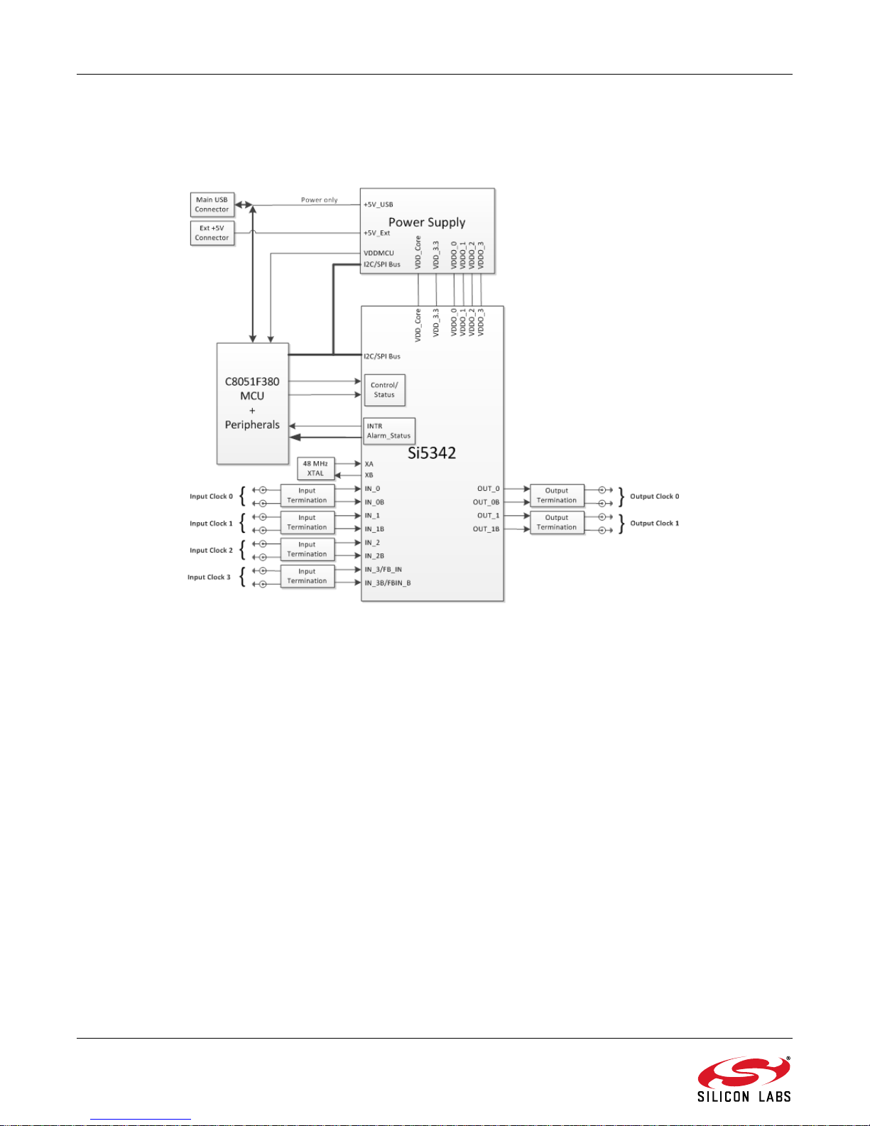
1. Si5342-EVB Functional Block Diagram
Below is a functional block diagram of the Si5342-EVB. This EVB can be connected to a PC via the main USB
connector for programming, control, and monitoring. See section “3. Quick Start” or section “9. Installing
ClockBuilderPro (CBPro) Desktop Software” for more information.
Figure 2. Si5342-EVB Functional Block Diagram
2 Rev. 1.0

Si5342-EVB
2. Si5342-EVB Support Documentation and ClockBuilderPro Software
All Si5342 schematics, BOMs, User’s Guides, and software can be found online at the following link:
http://www.silabs.com/products/clocksoscillators/pages/si538x-4x-evb.aspx
3. Quick Start
1. Install ClockBuilderPro desktop software from http://www.silabs.com/CBPro.
2. Connect a USB cable from Si5342-EVB to the PC where the software was installed.
3. Leave the jumpers as installed from the factory, and launch the ClockBuilderPro software.
4. You can use ClockBuilderPro
5. For the Si5342 data sheet, go to http://www.silabs.com/timing.
to create, download, and run a frequency plan on the Si5342-EVB.
Rev. 1.0 3

Si5342-EVB
4. Jumper Defaults
Si5342EVBJumperDefaults
Location Type
I=Installed
0=Open
JP1 2 pin I
JP2 2 pin I
JP3 2 pin O
JP4 2 pin O
JP5 3 pin 1 to 2 (USB)
JP13 2 pin O
Location Type
I=Installed
0=Open
Refer to the Si5342 EVB schematics for the functionality associated with each jumper.
4 Rev. 1.0
J17 5x2 Hdr All 5 installed

5. Status LEDs
Si5342-EVB
Si5342EVBStatusLEDs
Location Silkscreen Color StatusFunctionIndication
D5 INTRB Blue
D7 LOLB Blue
D14 LOS0B* Blue
D15 LOS1B* Blue
D16 LOS3B* Blue
D17 LOS2B* Blue
D11 +5V MAIN Green
D12 READY Green
D13 BUSY Green
Note: The LOSxB LEDs may be dim when the EVB is first plugged in. Once
ClockBuilderPro is launched, the LEDs will begin to function normally.
D5, D7, D14, D15, D16, and D17 are status LEDs indicating the device alarms currently asserted. D11 is
illuminated when USB +5 V supply voltage is present. D12 and D13 are status LEDs showing on-board MCU
activity.
MCU INTR (Interrupt) active
MCU INTR (Interrupt) active
IN0 Loss of Signal indicator
IN0 Loss of Signal indicator
IN0 Loss of Signal indicator
IN0 Loss of Signal indicator
Main USB +5V present
MCU Ready
MCU Busy
Figure 3. Status LEDs
Rev. 1.0 5

Si5342-EVB
6. Clock Input Circuits (INx/INxB)
The Si5342-EVB has eight SMA connectors (IN0/IN0B–IN3/IN3B) for receiving external clock signals. All input
clocks are terminated as shown in Figure 4 below. Note input clocks are AC coupled and 50 ohm terminated. This
represents 4 differential input clock pairs. Single-ended clocks can be used by appropriately driving one side of the
differential pair with a single-ended clock. For details on how to configure inputs as single-ended, please refer to
the Si5342 data sheet. Typically a 0.1 F DC block is sufficient, however, 10 F may be needed for lower input
frequencies. Note that the EVB is populated with both DC block capacitor values.
Figure 4. Input Clock Termination Circuit
7. Clock Output Circuits (OUTx/OUTxB)
Each of the four output drivers (2 differential pairs) is AC coupled to its respective SMA connector. The output clock
termination circuit is shown in Figure 5 below. The output signal will have no DC bias. If DC coupling is required,
the AC coupling capacitors can be replaced with a resistor of appropriate value. The Si5342-EVB provides an
L-network at OUT0/OUT0B output pins for optional output termination resistors. Note that components with
schematic “NI” designation are not normally populated.
Figure 5. Output Clock Termination Circuit
6 Rev. 1.0
 Loading...