

Silicon Laboratories Si5340-EVB User Manual
Si5340-EVB
Si5340 EVALUATION BOARD USER’S G UIDE
Description
The Si5340-EVB is used for evaluating the Si5340 Low
Jitter Any-Frequency Clock Generator. The Si5340 uses
the patented MultisynthTM technology to generate up to
10 independent clock frequencies each with 0 ppm
synthesis error. The Si5340-EVB has 3 independent
input clocks, an optional feedback input clock for zero
delay mode, and 4 independent output clocks. The
Si5340-EVB can be controlled and configured using the
Clock Builder Pro
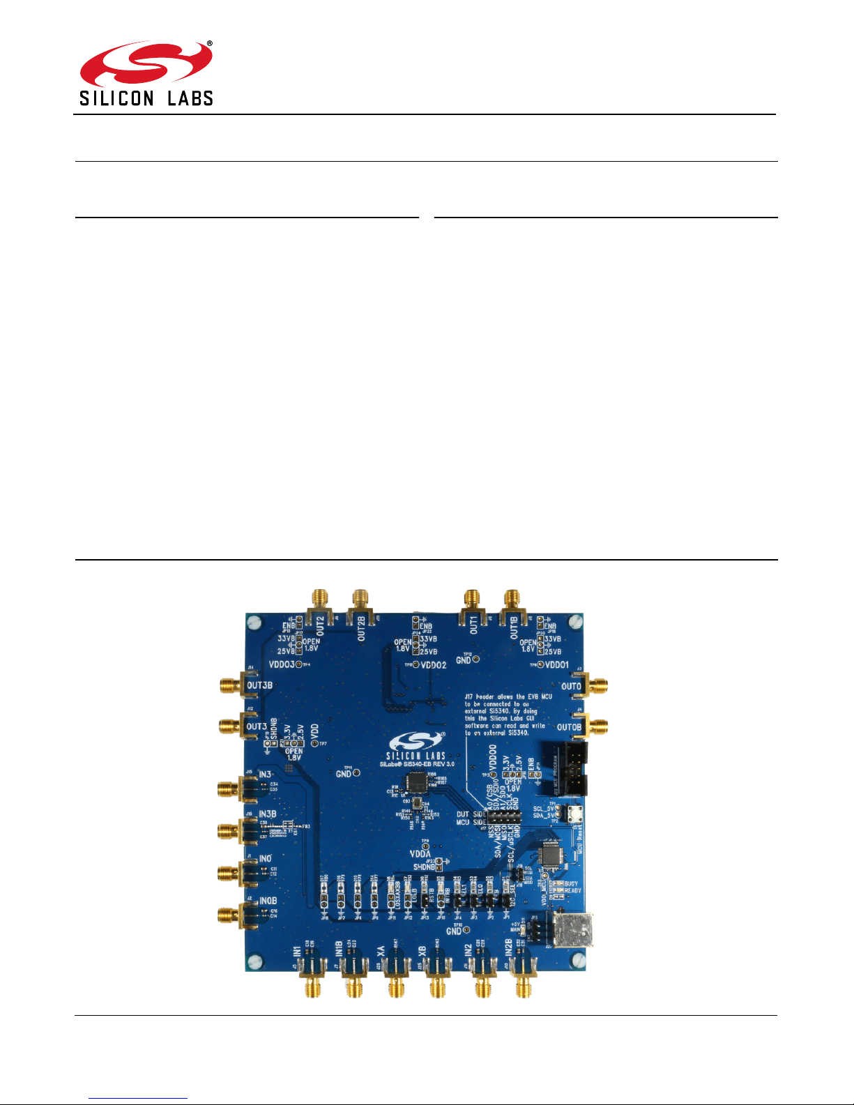
Si5340 Evaluation Board
TM
(CB ProTM) software tool.
Features
Powered from USB port or external power supply
Onboard 48 MHz XTAL allows free-run mode of
operation on the Si5340 or up to 3 input clocks for
synchronous clocking
Feedback clock input for optional zero delay mode
CBPro
device to operate from 3.3, 2.5, or 1.8 V.
CBPro GUI-programmable VDDO supplies allow
each of the 4 outputs to have its own supply voltage
selectable from 3.3, 2.5, or 1.8 V
CBPro GUI-controlled voltage, current, and power
measurements of VDD and all VDDO supplies.
Status LEDs for power supplies and control/status
signals of Si5340
SMA connectors for input and output clocks
TM
GUI-programmable VDD supply allows
Rev. 1.0 Copyright © 2015 by Silicon Laboratories Si5340-EVB

Si5340-EVB
1. Functional Block Diagram
Below is a functional block diagram of the Si5340-EVB. This EVB can be connected to a PC via the main USB
connector for programming, control, and monitoring. See Section “3. Quick Start” or Section “9. Installing
ClockBuilderPro (CBPro) Desktop Software” for more information.
Figure 1. Si5340-EVB Block Diagram
2 Rev. 1.0
Si5340-EVB
2. Si5340 EVB Support Documentation and ClockBuilderProTM Software
All Si5340 schematics, BOMs, User's Guides, and software can be found on-line at the following link:
http://www.silabs.com/products/clocksoscillators/pages/si538x-4x-evb.aspx
3. Quick Start
1. Install ClockBuilderPro™ desktop software: http://www.silabs.com/CBPro
2. Connect a USB cable from the Si5340-EVB to the PC where the software is installed.
3. Leave the jumpers as installed from the factory and launch the ClockBuilderPro™ software.
4. You can use ClockBuilderPro™ to create, download, and run a frequency plan on the Si5340-EVB.
5. For Si5340 data sheet go to: http://www.silabs.com/timing
4. Jumper Defaults
Si5340 EVB Jumper Defaults
Location Type I = Installed
0 = Open
JP1 2 pin I JP14 2 pin O
JP2 2 pin I JP15 2 pin O
JP3 2 pin O JP16 3 pin all open
JP4 2 pin O JP17 3 pin all open
JP5 3 pin 1 to 2 JP18 2 pin O
JP6 2 pin O JP19 2 pin O
JP7 2 pin O JP20 3 pin all open
JP8 2 pin O JP21 3 pin all open
JP9 2 pin O JP22 2 pin O
JP10 2 pin O JP23 2 pin O
JP11 2 pin O JP24 3 pin all open
JP12 2 pin O
JP13 2 pin O JP17 5x2 Hdr All 5 installed
Location Type I = Installed
0 = Open
Note: Refer to the Si5340 EVB schematics for the functionality associated with each jumper.
Rev. 1.0 3

Si5340-EVB
5. Status LEDs
Si5340 EVB Status LEDs
Location Silkscreen Color Status Function Indication
D5 INTRB Blue DUT Interrupt
D7 LOLB Blue DUT Loss of Lock
D8 LOSXAXBB Blue DUT Loss of Reference
D11 +5V MAIN Green Main USB +5V present
D12 READY Green MCU Ready
D13 BUSY Green MCU Busy
D11 is illuminated when USB +5V supply voltage is present. D12 and D13 are status LEDs showing on-board MCU
activity.
Figure 2. Status LEDs
4 Rev. 1.0
Si5340-EVB
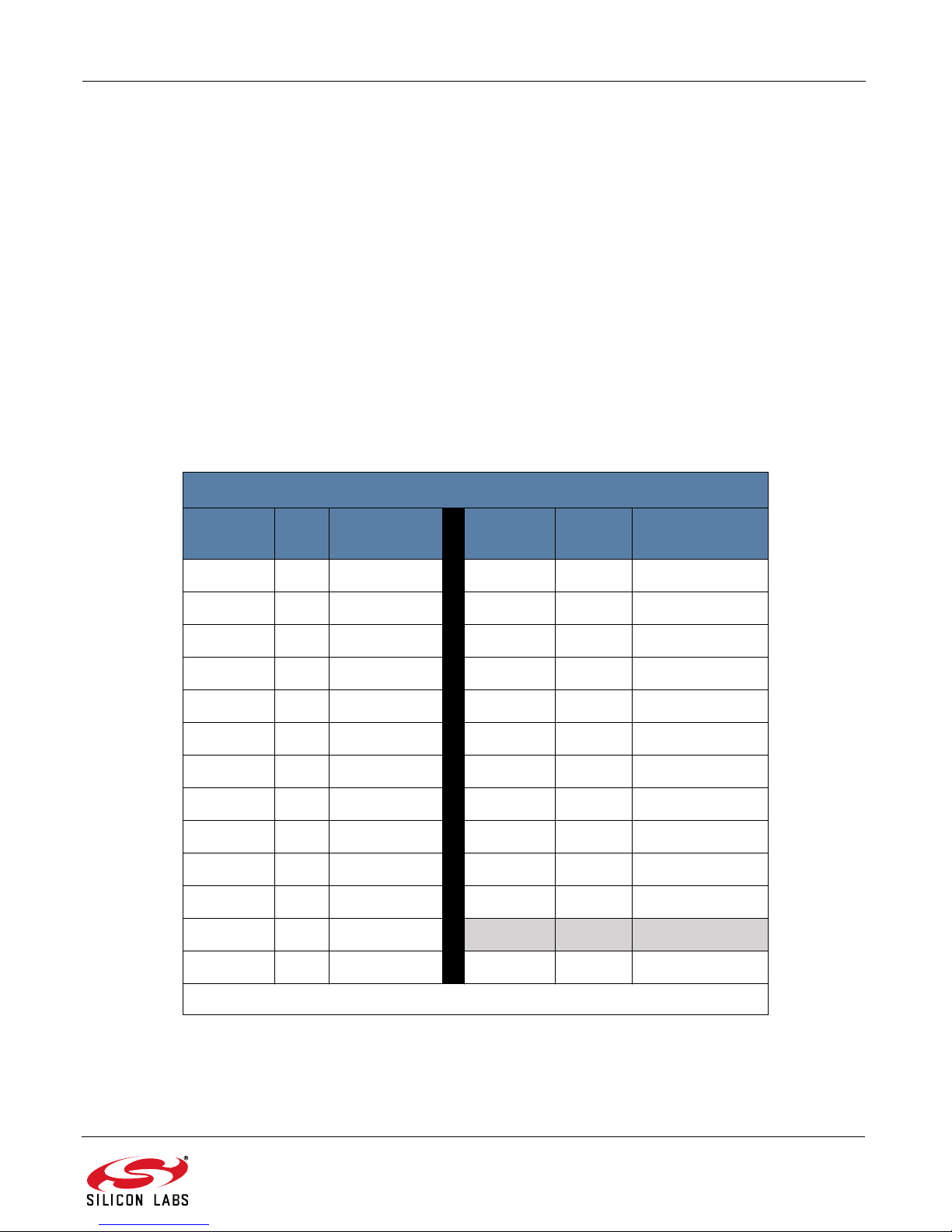
6. External Reference Input (XA/XB)
An external reference (XTAL) is used in combination with the internal oscillator to produce an ultra-low jitter
reference clock for the DSPLL and for providing a stable reference for the free-run and holdover modes. The
Si5340-EVB can also accommodate an external reference clock instead of a crystal. To evaluate the device with a
REFCLK, C93 and C94 must be populated and the XTAL removed (see Figure 3 below). The REFCLK can then be
applied to J25 and J26.
Figure 3. External Reference Input Circuit
7. Clock Input Circuits (INx/INxB and FB_IN/FB_INB)
The Si5340-EVB has eight SMA connectors (IN0/IN0B – IN2/IN2B and FB_IN/FB_INB) for receiving external clock
signals. All input clocks are terminated as shown in Figure 4 below.
Input clocks are AC coupled and 50- terminated. This represents 4 differential input clock pairs. Single-ended
clocks can be used by appropriately driving one side of the differential pair with a single-ended clock. For details on
how to configure inputs as single-ended, please refer to the Si5340 data sheet.
Figure 4. Input Clock Termination Circuit
Rev. 1.0 5
Si5340-EVB
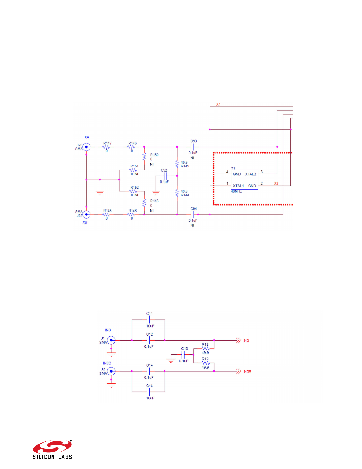
8. Clock Output Circuits (OUTx/OUTxB)
Each of the 8 outputs (4 differential pairs) is AC coupled to its respective SMA connector. The output clock
termination circuit is shown in Figure 5 below. The output signal has no DC bias. If DC coupling is required, the AC
coupling capacitors can be replaced with a resistor of appropriate value. The Si5340-EVB provides pads for
optional output termination resistors and/or low frequency capacitors.
Note: Components with schematic “NI” designation are not normally populated on the Si5340-EVB and provide locations on
the PCB for optional DC/AC terminations by the end user.
Figure 5. Output Clock Termination Circuit
9. Installing ClockBuilderPro (CBPro) Desktop Software
To install the CBPro software on any Windows 7 (or later version) PC, do the following:
1. Go to http://www.silabs.com/CBPro/ and download ClockBuilderPro™ software.
2. Installation instructions and User’s Guide for ClockBuilderPro™ can be found at the download link shown
above. Please follow the instructions as indicated.
10. Using the Si5340 EVB
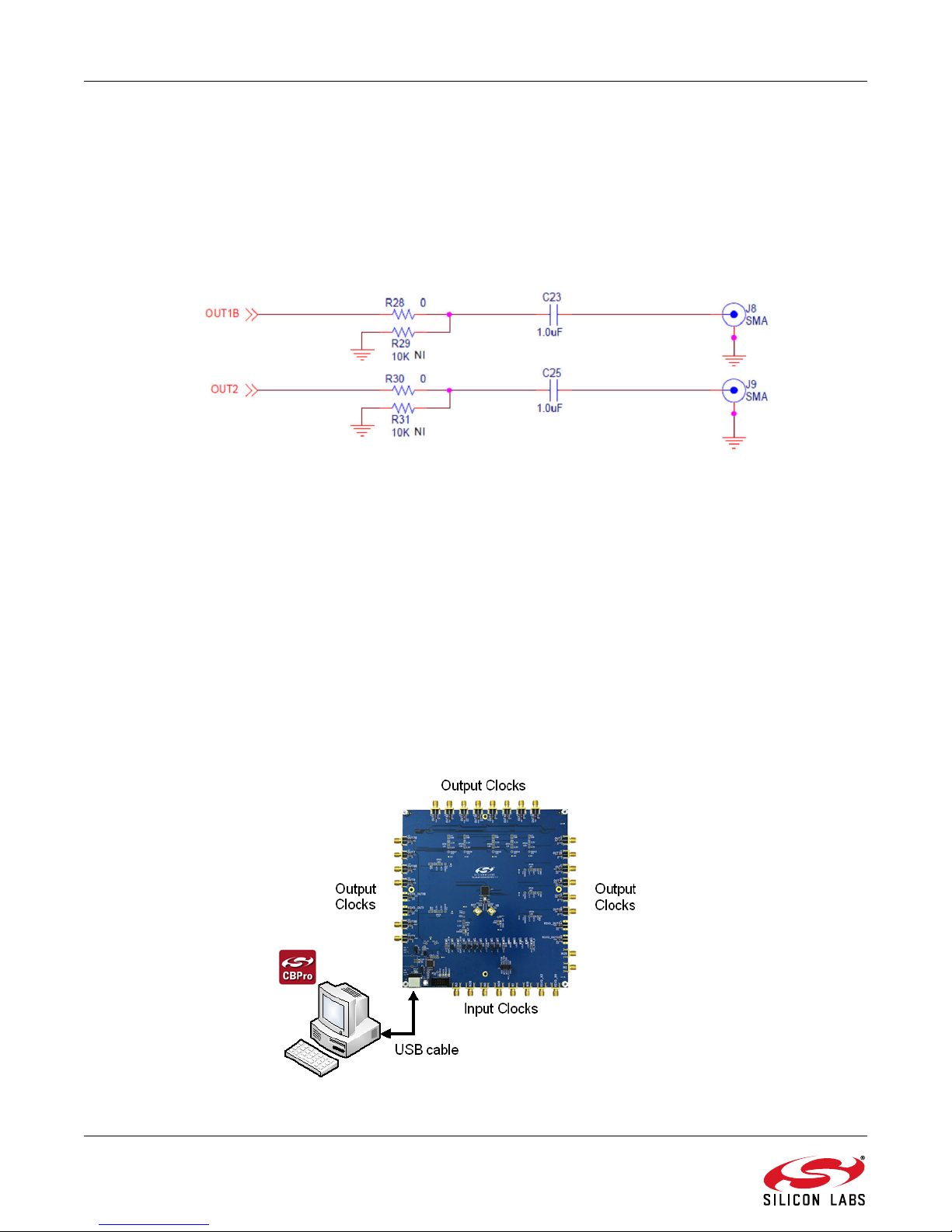
10.1. Connecting the EVB to Your Host PC
Once the ClockBuilderPro™ software in installed, connect the PC to the EVB with a USB cable as illustrated in
Figure 6.
6 Rev. 1.0
Figure 6. EVB Connection Diagram
 Loading...