

Silicon Laboratories Si53154-EVB User Manual
Si53154-EVB
Si53154
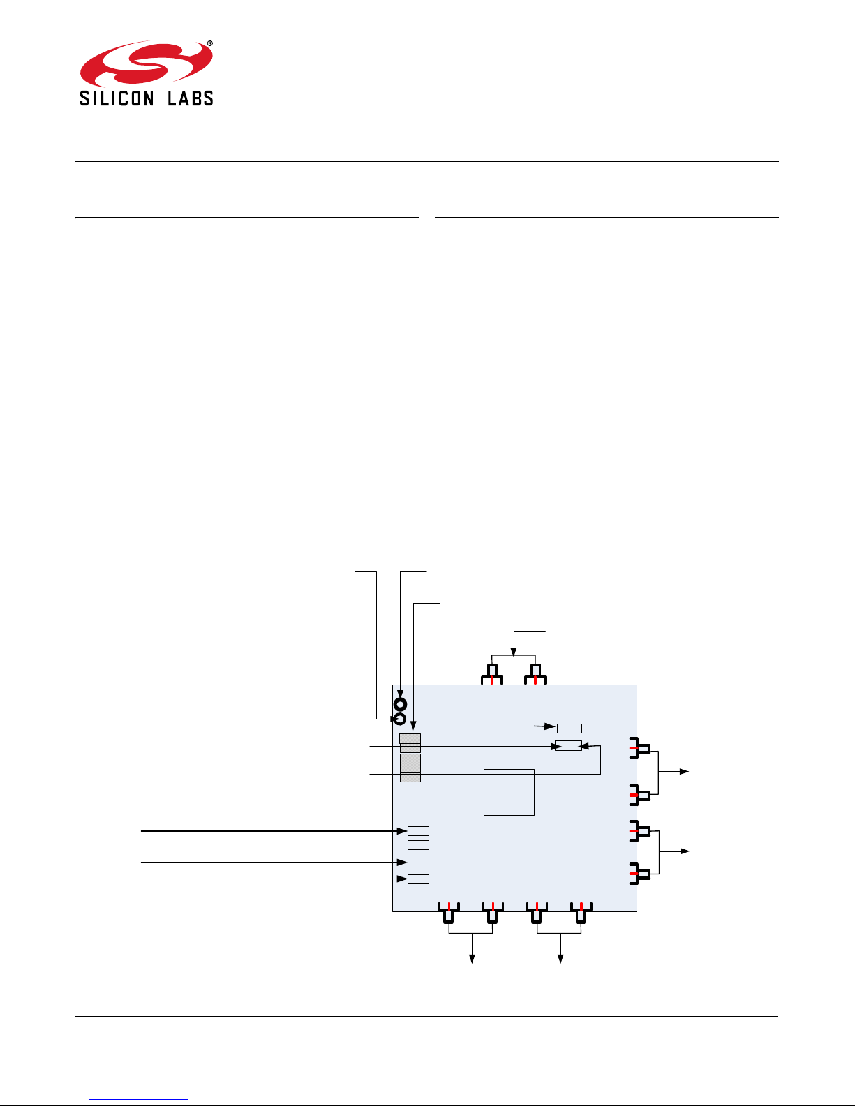
SRC3
connection
for
application
SRC2
connection
for
application
SRC1
connection for
application
VDD = 3.3V
power supply
GND
SDATA
SCLK
SRC0
connection for
application
DIFF3 Output Enable
DIFF1 Output Enable
DIFF2 Output Enable
DIFF0 Output Enable
Power connectors
Differential
Clock Input
Si53154 EVALUATION BOARD USER’S GUIDE
Description
The Si53154 is a four port PCIe clock buffer compliant
to the PCIe Gen1, Gen2 and Gen3 standards. The
Si53154 is a 24-pin QFN device that operates on a
3.3 V power supply and can be controlled using SMBus
signals along with hardware control input pins. The
device is spread aware and accepts a frequency spread
differential clock frequency range from 100 to 210 MHz.
The connections are described in this document.
EVB Features
This document is intended to be used in conjunction
with the Si53154 device and data sheet for the following
tests:
PCIe Gen1, Gen2, Gen3 compliancy
Power consumption test
Jitter performance
Testing out I
In-system validation where SMA connectors are
present
2
C code for signal tuning
Rev. 0.1 1/12 Copyright © 2012 by Silicon Labs Si53154-EVB
Si53154-EVB
I2C connect -For I2C read and
write. In sequence SData, Gnd,
SCLK from left to right
.
p
DIFF2 Differential output
DIFF1 Differential output
DIFF0 Differential output
1. Front Panel
Differential Buffer Input
for on Si53154-EVB only
3.3V Power Supply Connector
GND Connector
VDD Connectors
OE1 hardware input
control for DIFF1 output
No Connect
OE2 hardware input
control for DIFF2 output
OE0 hardware input
control for DIFF0 output
OE_DIFF3 hardware input
control for DIFF3 out
DIFF3 Differential output
ut
Si53154 device mount
Figure 1. Evaluation Module Front Panel
Table 1. Input Jumper Settings
Jumper Label Type Description
OE0 I
OE1 I
OE2 I
OE3 I
SDATA I/O
SCLK I
OE0, 3.3 V Input for Enabling DIFF0 Clock Output.
1 = DIFF0 enabled, 0 = DIFF0 disabled.
OE1, 3.3 V Input for Enabling DIFF1 Clock Output.
1 = DIFF1 enabled, 0 = DIFF1 disabled.
OE2, 3.3 V Input for Enabling DIFF2 Clock Output.
1 = DIFF2 enabled, 0 = DIFF2 disabled.
OE3, 3.3 V Input for Enabling DIFF3 Clock Output.
1 = DIFF3 enabled, 0 = DIFF3 disabled.
SMBus-Compatible SDATA.
SMBus-Compatible SCLOCK.
2 Rev. 0.1
 Loading...