

Silicon Laboratories Si52147 User Manual
Si52147-EVB
Si52147
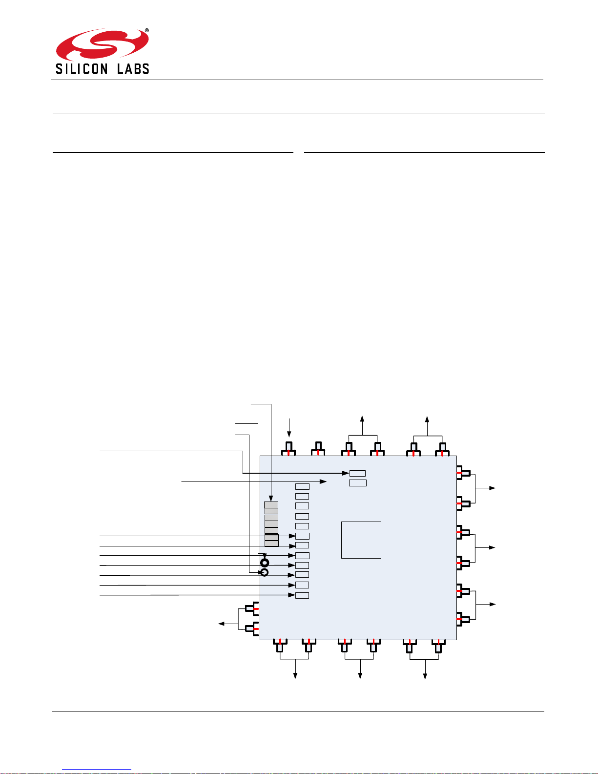
DIFF5
connection
for
application
DIFF4
connection
for
application
DIFF2 connection
for application
VDD = 3.3 V
power supply
GND
SDATA
GND
SCLK
DIFF1 connection for
application
Spread Enable Control
DIFF2 Output Enable
DIFF4/DIFF5 Output Enable
DIFF6/DIFF8 Output Enable
Power connectors
External
Clock Input
DIFF3 connection
for application
DIFF6
connection
for
application
DIFF7 connection
for application
DIFF8 connection
for application
DIFF3 Output Enable
DIFF1 Output Enable
DIFF0 Output Enable
DIFF0 connection
for application
CKPWRGD/Power down enable
SDATA/SCLK
Si52147 EVALUATION BOARD USER’S GUIDE
Description
The Si52147 is a nine port PCIe clock generator
compliant to the PCIe Gen1, Gen2 and Gen3 standa rds.
The Si52147 is a 48-pin QFN device that operates on a
3.3 V power supply and can be controlled using SMBus
signals along with hardware control input pins.The
differential outputs support spread spectrum and can be
controlled through SSON input pin. The Si52147 needs
a crystal or clock input of 25 MHz. The connections are
described in this document.
EVB Features
This document is intended to be used in conjunction
with the Si52147 device and data sheet for the following
tests:
PCIe Gen1, Gen2, Gen3 compliancy
Power consumption test
Jitter performance
Testing out I
In-system validation where SMA connectors are
present
2
C code for signal tuning
Rev. 0.1 1/12 Copyright © 2012 by Silicon Labs Si52147-EVB

Si52147-EVB
I2C connect -For I2C read and
write. In sequence SData, Gnd,
SCLK from left to right
.
DIFF1 Differential output
DIFF3 Differential output
control for Spread enable,
DIFF2, DIFF3, DIFF4 though
DIFF5 and DIFF6 through
DIFF4 Differential output
DIFF5 Differential output
1. Front Panel
External Clock Input for
on Si52147-EVB only
VDD Connectors
OE0 and OE1 hardware input
control for DIFF0 and DIFF1
outputs respectively
GND Connector
3.3 V Power Supply
SSON, OE2, OE3, OE4/5 and
OE6/8 hardware inputs
DIFF8 outputs respectively
DIFF0 Differential output
Si52147 device mount
DIFF8 Differential output
DIFF7 Differential output
CKPWRGD/ Power down input
control
DIFF6 Differential output
DIFF2 Differential output
Jumper Label Type Description
CLKPWGD/PD
OE0 I
OE1 I
OE2 I
OE3 I
OE4/5 I
OE6/8 I
Figure 1. Evaluation Module Front Panel
Table 1. Input Jumper Settings
OE0, 3.3 V Input for Enabling DIFF0 Clock Output.
1 = DIFF0 enabled, 0 = DIFF0 disabled.
OE1, 3.3 V Input for Enabling DIFF1 Clock Output.
1 = DIFF1 enabled, 0 = DIFF1 disabled.
OE2, 3.3 V Input for Enabling DIFF2 Clock Output.
1 = DIFF2 enabled, 0 = DIFF2 disabled.
OE3, 3.3 V Input for Enabling DIFF3 Clock Output.
1 = DIFF3 enabled, 0 = DIFF3 disabled.
OE4/5, 3.3 V Input for Enabling DIFF4 and DIFF5 Clock Outputs.
1 = DIFF4 & DIFF5 enabled, 0 = DIFF4 & DIFF5 disabled.
OE6/8, 3.3 V Input for Enabling DIFF6, DIFF7 and DIFF8 Clock Outputs.
1 = DIFF6, DIFF7 & DIFF8 enabled, 0 = DIFF6, DIFF7 & DIFF8 disabled.
I
3.3 V LVTTL Input.
After CLKPWGD (active high) assertion, this pin becomes a real-time input for
asserting power down (active low).
2 Rev. 0.1

Table 1. Input Jumper Settings (Continued)
Si52147-EVB
SSON I
SDATA I/O
SCLK I
SSON Frequency
0 100.00 OFF
1 100.00 –0.5
SSON Input, 3.3 V-Tolerant Active Input for Spread s election on the Output.
Internal 100 k pulldown.
1 = –0.5% Spread enabled, 0 = Spread disabled.
SMBus-Compatible SDATA.
SMBus-Compatible SCLOCK.
Table 2. Spread Selection
(MHz)
Spread
(%)
Default Va lue for SSON= 0
Note
Rev. 0.1 3
 Loading...