

Preliminary Rev. 0.41 8/01 Copyright © 2001 by Silicon Laboratories Si5100-DS041
This information applies to a product under development. Its characteristics and specifications are subject to change without notice.
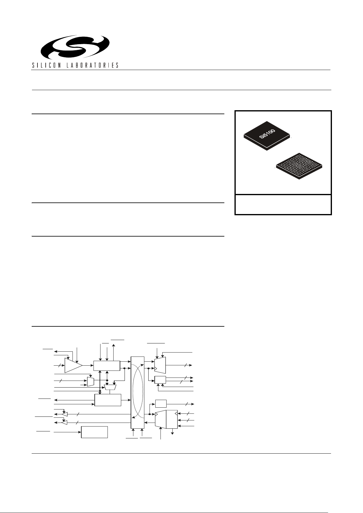
Si5100
SiPHY
TM
OC-48/STM-16 SONET/SDH TRANSCEIVER
Features
Complete low power, high speed, SONET/SDH transceiver with
integrated limiting amp, CDR, CMU, and MUX/DEMUX
Applications
Description
The Si5100 is a complete low-power transceiver for high-speed serial
communication systems operating between 2.5 Gbps and 2.7 Gbps. The receive
path consists of a fully integrated limiting amplifier, clock and data recovery unit
(CDR), and 1:16 deserializer. The transmit path combines a low jitter clock
multiplier unit (CMU) with a 16:1 serializer. The CMU uses Silicon Laboratories’
DSPLL
™
technology to provide superior jitter performance while reducing design
complexity by eliminating external loop filter components. To simplify BER
optimization in long haul applications, programmable slicing and sa mple phase
adjustment are supported.
The Si5100 operates from a single 1.8 V supply over the industrial temperature
range (–40°C to 85°C).
Functional Block Diagram
! Data Rates Supported:
OC-48/STM-16 and 2.7 Gbps FEC
! Low Power Operation 1.2 W (typ)
! DSPLL™ Based Clock Multiplier Unit
w/ Selectable Loop Filter Bandwidths
! Integrated Limiting Amplifier
! Loss-of-Signal (LOS) Alarm
! Diagnostic and Line Loopbacks
! SONET Compliant Loop Timed
Operation
! Programmable Slicing Level and
Sample Phase Adjustment
! LVDS Parallel Interface
! Single Supply 1.8 V Operation
! 15 x 15 mm BGA Package
! Sonet/SDH Transmission
Systems
! Optical Transceiver Modules
! Sonet/SDH Test Equipment
TXDO UT
RXDOUT[15:0]
TXDIN[15:0]
RXCLK1
RXCLK2
TXCLK16OUT
FIFORST
RXCLK2DIV
FIFOERR
1:16
DEMUX
16:1
MUX
FIFO
TXCLK16IN
RXSQLCH
DLBKLLBK
TXMSBSEL
RXMSBSEL
XCLKOUT
TXSQLCH
2
32
2
2
2
RXCLK2DSBL
2
LPTM
RXDIN
REFCLK
TXLOL
Limiting
AMP
LOSLVL
LOS
LTR
DSPLL
tm
TX CM U
CDR
CLKDSBL
2
2
Loopback Control
TXCLK16IN
REFSEL
BWSEL
2
SLICELVL
PHASEADJ
RXLOL
32
REFRATE
RESET
Control
RESET
÷
÷
Ordering Information:
See page 23.
Si5100
Bottom View
PRELIMINARY DATA SHEET

Si5100
2 Preliminary Rev. 0.41

Si5100
Preliminary Rev. 0.41 3
TABLE OF CONTENTS
Section Page
Electrical Specifications . . . . . . . . . . . . . . . . . . . . . . . . . . . . . . . . . . . . . . . . . . . . . . . . . 4
Functional Description . . . . . . . . . . . . . . . . . . . . . . . . . . . . . . . . . . . . . . . . . . . . . . . . . . 11
Receiver . . . . . . . . . . . . . . . . . . . . . . . . . . . . . . . . . . . . . . . . . . . . . . . . . . . . . . . . . . . . . . 11
Limiting Amplifier . . . . . . . . . . . . . . . . . . . . . . . . . . . . . . . . . . . . . . . . . . . . . . . . . . . . 11
Clock and Data Recovery (CDR) . . . . . . . . . . . . . . . . . . . . . . . . . . . . . . . . . . . . . . . . 12
Deserialization . . . . . . . . . . . . . . . . . . . . . . . . . . . . . . . . . . . . . . . . . . . . . . . . . . . . . . 12
Auxiliary Clock Output . . . . . . . . . . . . . . . . . . . . . . . . . . . . . . . . . . . . . . . . . . . . . . . . 12
Data Squelch . . . . . . . . . . . . . . . . . . . . . . . . . . . . . . . . . . . . . . . . . . . . . . . . . . . . . . . 13
Transmitter . . . . . . . . . . . . . . . . . . . . . . . . . . . . . . . . . . . . . . . . . . . . . . . . . . . . . . . . . . . . 13
DSPLL™ Clock Multiplier Unit . . . . . . . . . . . . . . . . . . . . . . . . . . . . . . . . . . . . . . . . . . 13
Serialization . . . . . . . . . . . . . . . . . . . . . . . . . . . . . . . . . . . . . . . . . . . . . . . . . . . . . . . . 3
Loop Timed Operation . . . . . . . . . . . . . . . . . . . . . . . . . . . . . . . . . . . . . . . . . . . . . . . . . . . 14
Diagnostic Loopback . . . . . . . . . . . . . . . . . . . . . . . . . . . . . . . . . . . . . . . . . . . . . . . . . . . . 14
Line Loopback . . . . . . . . . . . . . . . . . . . . . . . . . . . . . . . . . . . . . . . . . . . . . . . . . . . . . . . . . 14
Bias Generation Circuitry . . . . . . . . . . . . . . . . . . . . . . . . . . . . . . . . . . . . . . . . . . . . . . . . 14
Reference Clock . . . . . . . . . . . . . . . . . . . . . . . . . . . . . . . . . . . . . . . . . . . . . . . . . . . . . . . . 14
Reset . . . . . . . . . . . . . . . . . . . . . . . . . . . . . . . . . . . . . . . . . . . . . . . . . . . . . . . . . . . . . . . . . 14
Voltage Reference Output . . . . . . . . . . . . . . . . . . . . . . . . . . . . . . . . . . . . . . . . . . . . . 14
Transmit Differential Output Circuitry . . . . . . . . . . . . . . . . . . . . . . . . . . . . . . . . . . . . . . 15
Si5100 Pinout: 195-Pin BGA . . . . . . . . . . . . . . . . . . . . . . . . . . . . . . . . . . . . . . . . . . . . . . 16
Pin Descriptions: Si5100 . . . . . . . . . . . . . . . . . . . . . . . . . . . . . . . . . . . . . . . . . . . . . . . . . 18
Ordering Guide . . . . . . . . . . . . . . . . . . . . . . . . . . . . . . . . . . . . . . . . . . . . . . . . . . . . . . . . . 24
Package Outline . . . . . . . . . . . . . . . . . . . . . . . . . . . . . . . . . . . . . . . . . . . . . . . . . . . . . . . . 25
Contact Information . . . . . . . . . . . . . . . . . . . . . . . . . . . . . . . . . . . . . . . . . . . . . . . . . . . . . 26
Si5100
4 Preliminary Rev. 0.41
Electrical Specifications
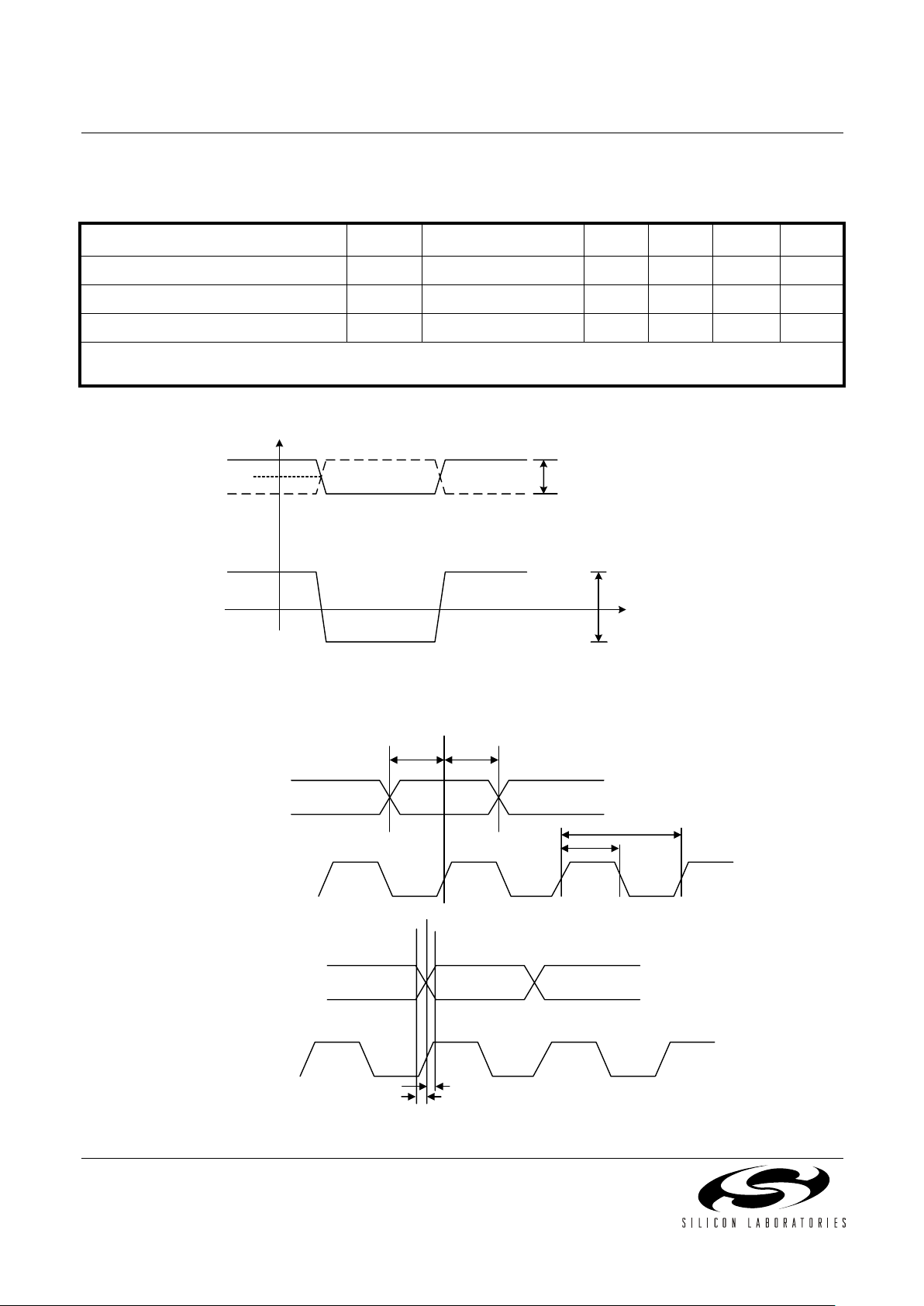
Figure 1. Differential Voltage Measurement
(RXDIN, RXDOUT, RXCLK1, RXCLK2, TXDIN, TXDOUT, TXCLKOUT, TXCLK16OUT, TXCLK16IN)
Figure 2. Data to Clock Delay
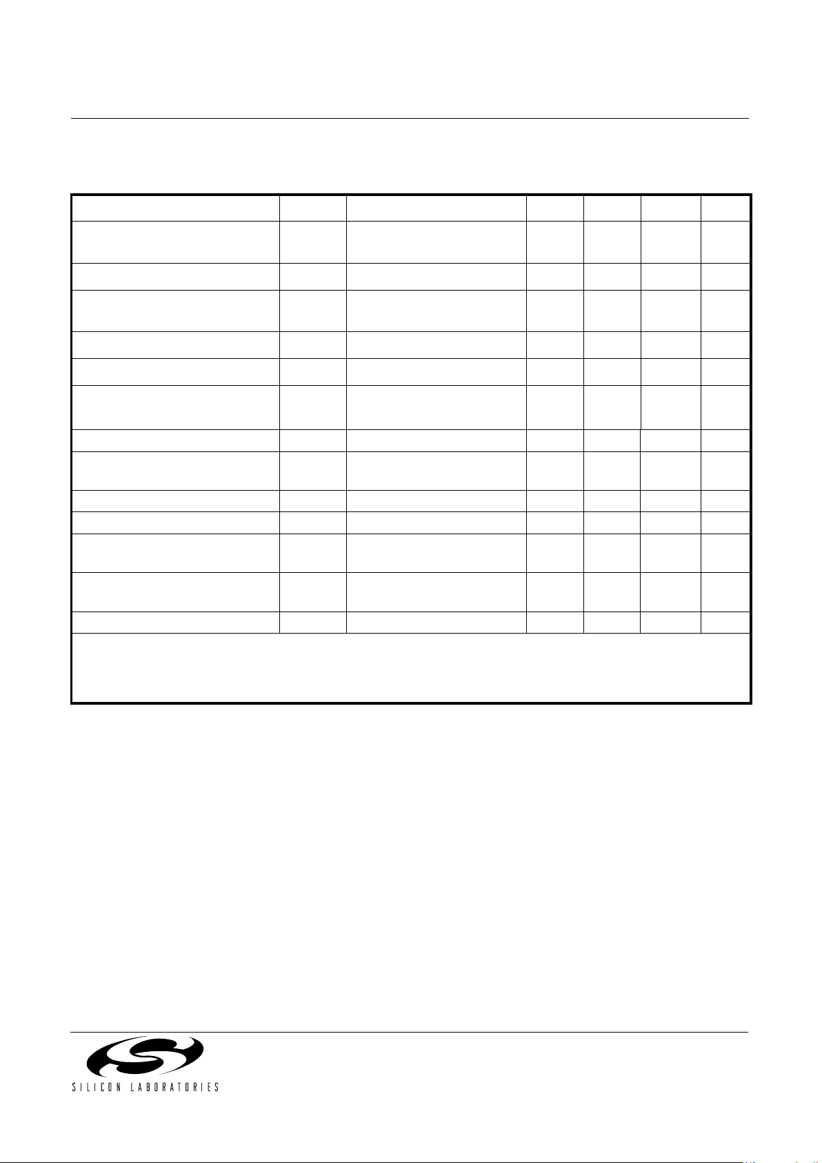
Table 1. Recommended Operating Conditions
Parameter Symbol Test Condition
Min
*
Typ
Max
*
Unit
Ambient Temperature T
A
–40 25 85 °C
LVTTL Output Supply Voltage V
DD33
1.71 — 3.47 V
Si5100 Supply Voltage V
DD
1.71 1.8 1.89 V
*Note: All minimum and maximum specifications are guaranteed and apply across the recommended operating conditions.
Typical values apply at nominal supply voltages and an operating temperature of 25°C unless otherwise stated.
V
IS
VID,VOD (V
ID
= 2VIS)
Differential
I/Os
Differential
Voltage Swing
Single Ended Voltage
Differential Peak-to-Peak Voltage
SIGNAL +
SIGNAL –
(SIGNAL +) – (SIGNAL –)
V
ICM
, V
OCM
V
t
TXDOUT,
TXDIN
TXCLKOUT,
TXCLK16IN
t
CP
t
hd
t
su
t
CH
RXDOUT
RXCLK1
t
cq1
t
cq2
Si5100
Preliminary Rev. 0.41 5
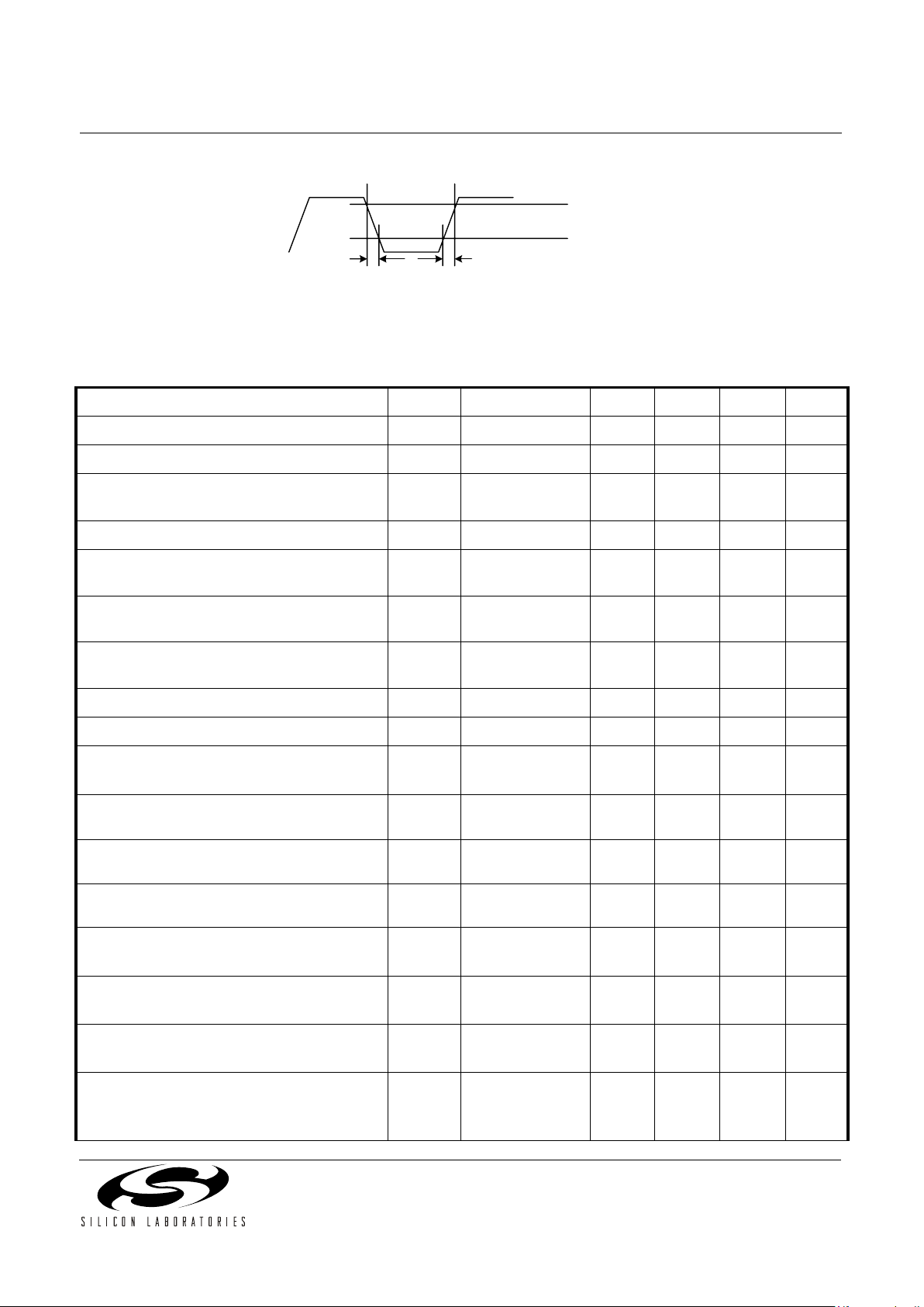
Figure 3. Rise/Fall Time Measurement
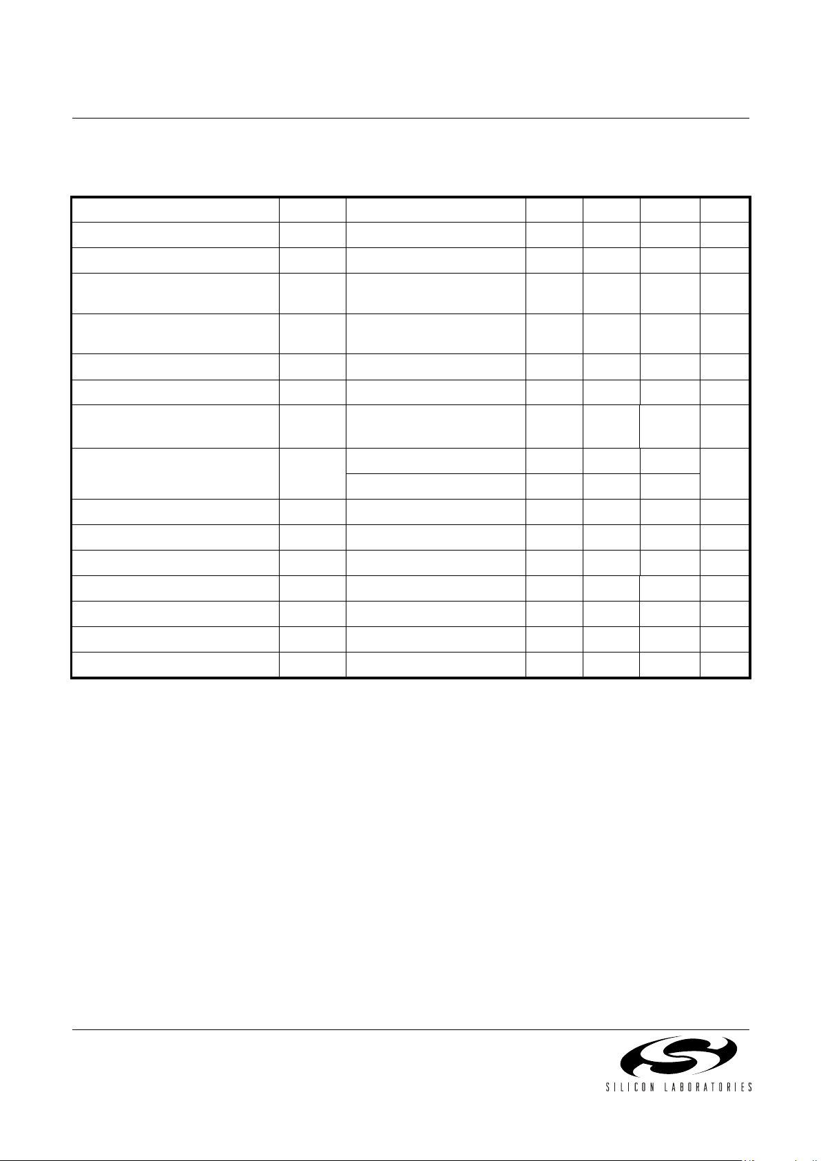
Table 2. DC Characteristics
(VDD = 1.8 V ±5%, TA = –40°C to 85°C)
Parameter Symbol Test Condition Min Typ Max Unit
Supply Current I
DD
—611TBDmA
Power Dissipation P
D
—1.2 TBDW
Voltage Reference (VREF) V
REF
VREF driving
10 k
Ω load
1.21 1.25 1.29 V
Common Mode Input Voltage (RXDIN) V
ICM
TBD 0.1 TBD V
Differential Input Voltage Swing (RXDIN) V
ID
See Figure 1 10 — 1.0 mV
(pk-pk)
Common Mode Output Voltage
(TXDOUT, TXCLKOUT)
V
OCM
.8 0.9 1.0 V
Differential Output Voltage Swing
(TXDOUT,TXCLKOUT), Differential pk-pk
V
OD
See Figure 1 800 1000 1200 mV
(pk-pk)
LVPECL Input Voltage HIGH (REFCLK) V
IH
1.975 2.3 2.59 V
LVPECL Input Voltage LOW (REFCLK) V
IL
1.32 1.6 1.99 V
L VPECL Input Voltage Swing,
Differential pk-pk (REFCLK)
V
ID
See Figure 1 250 — 2400 mV
(pk-pk)
L VPECL Internally Generated Input Bias
(REFCLK)
V
IB
1.6 1.95 2.3 V
LVDS Input High Voltage
(TXDIN,TXCLK16IN)
V
IH
——2.4V
LVDS Input Low Voltage
(TXDIN,TXCLK16IN)
V
IL
0.0 — — V
LVDS Input Voltage, Single Ended pk-pk
(TXDIN,TXCLK16IN)
V
ISE
100 — 600 mV
(pk-pk)
LVDS Output High Voltage
(RXDOUT,RXCLK1,RXCLK2,TXCLK16OUT)
V
OH1
100 Ω Load
Line-to-Line
TBD — 1.475 mV
LVDS Output Low Voltage
(RXDOUT,RXCLK1,RXCLK2,TXCLK16OUT)
V
OL1
100 Ω Load
Line-to-Line
0.925 — TBD V
LVDS Output Voltage, Dif fe rential pk-pk
(RXDOUT,RXCLK1,RXCLK2,TXCLK16OUT)
V
OSE
100 Ω Load
Line-to-Line,
Figure 1
500 — 800 mV
(pk-pk)
All Differential
IOs
t
F
t
R
80%
20%
Si5100
6 Preliminary Rev. 0.41
LVDS Common Mode Voltage
(RXDOUT,RXCLK1,RXCLK2,TXCLK16OUT)
V
CM
1.125 — 1.275 V
Input Impedance (TXDIN, TXCLK16IN,
REFCLK, RXDIN)
R
IN
Each input to
common mode
42 50 58 Ω
Output Short to GND
(RXDOUT,RXCLK1,RXCLK2,
TXCLK16OUT, TXDOUT,TXCLKOUT)
I
SC(–)
—25TBDmA
Output Short to V
DD
(RXDOUT, RXCLK1, RXCLK2,
TXCLK16OUT, TXDOUT, TXCLKOUT)
I
SC(+)
TBD –100 — µA
LVTTL Input Voltage Low
(RXMSBSEL, RXCLK2DIV, RXCLK2DSBL,
RXSQLCH
, REFSEL, L TR, RESET, MODE16
TXCLKDSBL, FIFORST, TXSQLCH
,
BWSEL, TXMSBSEL, DLBK
, LLBK, LPTM)
V
IL2
VDD33 = 3.3 V — — 0.8 V
VDD33 = 1.8 V — — 0.7
LVTTL Input Voltage High
(RXMSBSEL, RXCLK2DIV, RXCLK2DSBL,
RXSQLCH
, REFSEL, L TR, RESET, MODE16
TXCLKDSBL, FIFORST,TXSQLCH
,
BWSEL, TXMSBSEL, DLBK
, LLBK, LPTM)
V
IH2
VDD33 = 3.3 V 2.0 — — V
VDD33 = 1.8 V 1.7
LVTTL Input Low Current
(RXMSBSEL, RXCLK2DIV, RXCLK2DSBL,
RXSQLCH
, REFSEL, L TR, RESET, MODE16
TXCLKDSBL, FIFORST, TXSQLCH
,
BWSEL, TXMSBSEL, DLBK
, LLBK, LPTM)
I
IL
——10µA
LVTTL Input High Current
(RXMSBSEL, RXCLK2DIV, RXCLK2DSBL,
RXSQLCH
, REFSEL, L TR, RESET, MODE16
TXCLKDSBL, FIFORST, TXSQLCH
,
BWSEL, TXMSBSEL, DLBK
, LLBK, LPTM)
I
IH
——10µA
LVTTL Input Impedance
(RXMSBSEL, RXCLK2DIV, RXCLK2DSBL,
RXSQLCH
, REFSEL, L TR, RESET, MODE16
TXCLKDSBL, FIFORST, TXSQLCH
,
BWSEL, TXMSBSEL, DLBK
, LLBK, LPTM)
R
IN
10 — — kΩ
LVTTL Output Voltage Low
(LOS
, RXLOL, FIFOERR, TXLOL)
V
OL2
VDD33 = 1.8 V — — 0.4 V
VDD33 = 3.3 V — — 0.4
LVTTL Output Voltage High
(LOS
, RXLOL, FIFOERR, TXLOL)
V
OH2
VDD33 = 1.8 V 1.4 — — V
VDD33 = 3.3 V 2.4 — —
Table 2. DC Characteristics (Continued)
(VDD = 1.8 V ±5%, TA = –40°C to 85°C)
Parameter Symbol Test Condition Min Typ Max Unit
Si5100
Preliminary Rev. 0.41 7
Table 3. AC Characteristics (RXDIN, RXDOUT, RXCLK1, RXCLK2)
(VDD = 1.8 V ±5%, TA = –40°C to 85°C)
Parameter Symbol Test Condition Min Typ Max Unit
Output Clock Frequency
(RXCLK1)
f
clkout
See Figure 2 — 155 167 MHz
Duty Cycle (RXCLK1, RXCLK2) tch/tcp, Figure 2 45 — 55 %
Output Rise and Fall Times
(RXCLK1, RXCLK2, RXDOUT)
t
R,tF
Figure 3 — 50 — ps
Data Invalid Prior to RXCLK1 t
cq1
Figure 2 — — 200 ps
Data Invalid After RXCLK1 t
cq2
Figure 2 — — 200 ps
Input Return Loss (RXIN) 100 kHz–2.5 GHz
2.5 GHz–4.0 GHz
18.7
TBD
—
—
—
—
dB
dB
Slicing Adjust Dynamic Range SLICELVL = 200–800 mV –20 — 20 mV
Slicing Level Offset
1
(referred to RXDIN)
SLICELVL = 200–800 mV –500 — 500
µV
Slicing Level Accuracy VSLICE –5 — 5 %
Sampling Phase Adjustment
2
PHASEADJ = 200–800 mV –22.5° — 22.5°
LOS Threshold Dynamic Range LOSLVL = 200–800 mV 10 — 50 mV
pk-pk
LOS Threshold Offset
3
(referred to RXDIN)
LOSLVL = 200–800 mV –500 — 500
µV
LOS Threshold Accuracy VLOS –5 — 5 %
Note:
1. Slice level (referred to RXDIN) is calculated as follows: VSLICE = (SLICE_LVL – 0.4"VREF)/15.
2. Sample Phase Offset is calculated as follows: PHASE OFFSET = 22.5°(PHASEADJ – 0.4
"
VREF)/0.3
3. LOS Threshold voltage (referred to RXDIN) is calculated as follows: VLOS = 30 mV + (LOS_LVL – 0.4"VREF)/15.
Si5100
8 Preliminary Rev. 0.41
Table 4. AC Characteristics (TXCLK16OUT, TXCLK16IN, TXCLKOUT, TXDIN, TXDOUT)
(V
DD =
1.8 V ±5%, TA = –40°C to 85°C)
Parameter Symbol Test Condition Min Typ Max Unit
TXCLKOUT Frequency f
clkout
—2.52.7GHz
TXCLKOUT Duty Cycle tch/tcp, Figure 2 45 — 55 %
Output Rise Time
(TXCLKOUT, TXDOUT)
t
R
Figure 3 — 25 — ps
Output Fall Time
(TXCLKOUT, TXDOUT)
t
F
Figure 3 — 25 — ps
TXCLKOUT Setup to TXDOUT t
su
Figure 2 25 — — ps
TXCLKOUT Hold From TXDOUT t
hd
Figure 2 25 — — ps
Output Return Loss 100 kHz–2.5 GHz
2.5 GHz–4.0 GHz
TBD
TBD
—
—
—
—
dB
dB
TXCLK16OUT Frequency f
CLKIN
MODE16 = 1 — 622 667 MHz
MODE16 = 0 — 155 167
TXCLK16OUT Duty Cycle tch/tcp, Figure 2 40 — 60 %
TXCLK16OUT Rise & Fall Times t
R
, t
F
100 — 300 ps
TXDIN Setup to TXCLK16IN t
DSIN
——300ps
TXDIN Hold from TXCLK16IN t
DHIN
——300ps
TXCLK16IN Frequency f
CLKIN
—155167MHz
TXCLK16IN Duty Cycle tch/tcp, Figure 2 40 — 60 %
TXCLK16IN Rise & Fall Times t
R
, t
F
100 — 300 ps

Si5100
Preliminary Rev. 0.41 9
Table 5. AC Characteristics (Receiver PLL)
(VDD = 1.8 V ± 5%, TA = –40°C to 85°C)
Parameter Symbol Test Condition Min Typ Max Unit
Jitter To lerance J
TOL(PP)
f = 600 Hz 15 30 — UI
PP
f = 6000 kHz 1.5 3.0 — UI
PP
f = 100 kHz 1.5 3.0 — UI
PP
f = 1 MHz 0.15 0.3 — UI
PP
Acquisition Time T
AQ
——20 µs
Input Reference Clock Frequency RC
FREQ
REFRATE = 1 — 155 167 MHz
REFRATE = 0 — 78 83 MHz
Reference Clock Duty Cycle RC
DUTY
40 50 60 %
Reference Clock Frequency
Tolerance
RC
TOL
–100 — 100 ppm
Frequency Difference at which
Receive PLL goes out of Lock
(REFCLK compared to the
divided down VCO clock)
LOL TBD 600 1000 ppm
Frequency Difference at which
Receive PLL goes into Lock
(REFCLK compared to the
divided down VCO clock)
LOCK TBD 300 TBD ppm
Note: Bellcore specifications: GR-1377-CORE, Issue 5, December 1998.
Table 6. AC Characteristics (Transmitter Clock Multiplier)
(VDD = 1.8 V ± 5%, TA = –40°C to 85°C)
Parameter Symbol Test Condition Min Typ Max Unit
Jitter Generation J
GEN(RMS)
PRBS 23 0.005 TBD UI
RMS
Jitter Transfer Bandwidth J
BW
BWSEL = 0 — — 6 kHz
BWSEL = 1 — — 25 kHz
Jitter Transfer Peaking — 0.05 0.1 dB
Acquisition Time T
AQ
Valid REFCLK — — 20 µs
Input Reference Clock Frequency RC
FREQ
REFRATE = 1 — 155 167 MHz
REFRATE = 0 — 78 84 MHz
Input Reference Clock Duty
Cycle
RC
DUTY
40 — 60 %
Input Reference Clock Frequency
Tolerance
RC
TOL
–100 — 100 ppm
Note: Bellcore specifications: GR-1377-CORE, Issue 5, December 1998.

Si5100
10 Preliminary Rev. 0.41
Table 7. Absolute Maximum Ratings
Parameter Symbol Value Unit
DC Supply Voltage V
DD
–0.5 to TBD V
LVTTL Input Voltage V
DD33
–0.5 to 3.6 V
Differential Input Voltages V
DIF
–0.3 to (VDD+ 0.3) V
Maximum Current any output PIN ±50 mA
Operating Junction Temperature T
JCT
–55 to 150 °C
Storage Temperature Range T
STG
–55 to 150 °C
Package Temperature
(soldering 10 seconds)
275
°C
ESD HBM Tole ra nc e (1 00 pf, 1.5 k
Ω)TBDV
Note: Permanent device damage may occur if the above Absolute Maximum Rati ngs are exceeded. Functional operation
should be restricted to the conditions as specified in the operational sections of this data sheet. Exposure to absolute
maximum rating conditions for extended periods may affect device reliability.
Table 8. Thermal Characteristics
Parameter Symbol Test Condition Value Unit
Thermal Resistance Junction to Ambient ϕ
JA
Still Air 38 °C/W

Si5100
Preliminary Rev. 0.41 11
Functional Description
The Si5100 transceiver is a low power, fully integrated
serializer/deserializer that provides significant margin to
all SONET/SDH jitter specifications. The device
operates from 2.5–2.7 Gbps making it suitable for OC48/STM-16, and OC-48/STM-16 applications that use
15/14 forward error correction (FEC) coding. The low
speed receive/transmit interface uses low-power LVDS
inputs and outputs.
Receiver
The receiver within the Si5100 includes a precision
limiting amplifier, jitter tolerant clock and data recovery
unit (CDR), and 1:16 demultiplexer. In addition,
programmable data slicing and sampling phase
adjustment are provided to support bit-error-rate (BER)
optimization for long haul applications.
Limiting Amplifier
The Si5100 incorporates a high sensitivity limiting
amplifier with sufficient gain to directly accept the output
of transimpedance amplifiers. High sensitivity is
achieved by using a digital calibration algorithm to
cancel out amplifier offsets. This algorithm achieves
superior offset cancellation by using statistical
averaging to remove noise that may degrade more
traditional calibration routines.
The limiting amplifier provides sufficient gain to fully
saturate with input signals that are less than 10 mV
peak-to-peak differential. In addition, input signals that
exceed 1 V peak-to-peak differential will not cause any
performance degradation.
Loss-of-Signal (LOS) Detection
The limiting amplifier includes circuitry that generates a
loss-of-signal (LOS) alarm when the input signal
amplitude on RXDIN falls below an externally controlled
threshold. The Si5100 can be configured to drive the
LOS
output low when the differential input amplitude
drops below a threshold set between ~8 mV and 50 mV
pk-pk differential. Approximately 3 dB of hysteresis
prevents unnecessary switching on LOS
.
The LOS threshold is set by applying a voltage between
0.20 V and 0.80 V to the LOSLVL input. The voltage
present on LOSLVL maps to an input signal threshold
as follows:
V
LOS
is the differential pk-pk LOS threshold referred to
the RXDIN input, V
LOSLVL
is the voltage applied to the
LOSLVL pin, and VREF is reference voltage output on
the VREF pin.
The LOS detection circuitry is disabled by tieing the
LOSLVL input to the supply (VDD). This forces the LOS
output high.
Slicing Level Adjustment
To support applications that require BER optimization,
the limiting amplifier provides circuitry that supports
adjustment of the 0/1 decision threshold (slicing level)
over a range of ±20 mV when referred to the interna lly
biased RXDIN input. The slicing level is set by applying
a voltage between 0.20 V and 0.80 V to the SLICELVL
input. The voltage present on SLICELVL sets the slicing
level as follows:
V
LEVEL
is the slicing level referred to the RXDIN input,
V
SLICE
is the voltage applied to the SLICE_LVL pin, and
VREF is reference voltage output on the VREF pin.
The slicing level adjustment may be disabled by tieing
the SLCLVL input to the supply (VDD). When slicing is
disabled, the slicing offset is set to 0.0 V relative to
internally biased input common mode voltage for
RXDIN.
Clock and Data Recovery (CDR)
The Si5100 uses an integrated CDR to recover clock
and data from a non-return to zer o (NRZ) signal input on
RXDIN. The recovered data clock is used to regene rate
the incoming data by sampling the output of the limiting
amplifier at the center of the NRZ bit period. The
recovered clock and data is then deserialized by a
multiplexer that can be configured to operate in either
1:16 or 1:4 mode. The deserialized data is output via a
LVDS compatible low speed inte rface (RXDOUT[15:0],
RXCLK1, and RXCLK2).
Sample Phase Adjustment
In applications where it is not desirable to recover data
by sampling in the center of the data eye, the Si5100
supports adjustment of the CDR sampling phase across
the NRZ data period. When sample phase adjustment is
enabled, the sampling instant used for data recovery
can be moved over a range of ±22.5
o
relative to the
center of the incoming NRZ bit period. Adjustment of the
sampling phase is desirable when data eye distortions
are introduced by the transmission medium.
The sample phase is set by applying a voltage between
0.20 V and 0.80 V to the PHASEADJ input. The voltage
present on PHASEADJ maps to sample phase offset as
follows:
V
LOS
V
LOSLVL
0.4xVREF–()
15
---------------------------------------------------------------
30 mV+=
V
LEVEL
V
SLICE
0.4xVREF–()
15
---------------------------------------------------------- -
=

Si5100
12 Preliminary Rev. 0.41
Phase Offset is the sampling offset in degrees from the
center of the data eye, V
PHASE
is the voltage applied to
the PHASEADJ pin, and VREF is reference voltage
output on the VREF pin. A positive phase offset will
adjust the sampling point to lead the default sampling
point in the center of the data eye, and a negative phase
offset will adjust the sampling point to lag the default
sampling point.
Data recovery using a sampling phase offset is disabled
by tieing the PHASEADJ input to the supply (VDD). This
forces a phase offset of 0
° to be used for data recovery.
Receiver Lock Detect
The Si5100 provides lock-detect circuitry that indicates
whether the PLL has achieved frequency lock with the
incoming data. This circuit compares the frequency of a
divided down version of the recovered clock with the
frequency of the supplied reference clock (REFCLK). If
the recovered clock frequency deviates from that of the
reference clock by the amount specified in Table 5 on
page 9, the PLL is declared out of lock, and the loss-oflock (RXLOL
) pin is asserted. In this state, the PLL will
try to reacquire lock with the incoming data stream.
During reacquisition, the recovered clock frequency
(RXCLK1 and RXCLK2) will drift over a ±1000 ppm
range relative to the supplied reference clock. The
RXLOL
output will remain asserted until the recovered
clock frequency is within the REFCLK frequency by the
amount specified in Table 5 on page 9.
Lock-to-Reference
In applications where it is desirable to maintain a stable
output clock during an alarm condition like loss-ofsignal, the lock-to-reference input (LTR
) can be used to
force a stable output clock. When LTR
is asserted, the
CDR is prevented from acquiring the data signal and the
CDR will lock the RXCLKOUT1 and RXCLKOUT2
outputs to the provided REFCLK. In typical applications,
the LOS
output would be tied to the LTR input to force a
stable output clock.
Deserialization
The Si5100 deserializes the high speed input for output
on a 16-bit parallel data bus RXDOUT[15:0]. The
demultiplexer used for deserialization can be configured
to output either 4 or 16 bit words via the MODE16 pin.
The data words are output on RXDOUT synchronous
with the rising edge of RXCLK1. This clock output is
derived by dividing down the recovered clock to the
output word rate. When the demultiplexer is configured
to output 4-bit data words, the data is output on
RXDOUT[3:0].
Serial Input to Parallel Output Relationship
The Si5100 provides the capability to select the order in
which the received serial data is mapped to the parallel
output bus RXDOUT[15:0]. The mapping of the receive
bits to the output data word is controlled by the RXMSBSEL input. If RXMSBSEL is tied low, the first bit
received is output on RXDOUT0 and the following bits
are output in order on RXDOUT1 through RXDOUT15.
If RXMSBSEL is tied high, the first bit received is output
on RXDOUT15 and the following bits are output in order
on RXDOUT14 through RXDOUT0.
Auxiliary Clock Output
To support the widest range of system timing
configurations, a second clock output is provided on
RXCLK2. This output can be configured to provide a
clock equal to either the parallel output word rate or
1/4th the output word rate. The divide factor used to
generate RXCLK2 is controlled via the RXCLKDIV2
input as described in the Pin Description table. In
applications which do not use RXCLK2, this output can
be powered down by forcing the RSCLK2DSBL input
high.
Data Squelch
During some system error conditions, such as LOS, it
may be desirable to force the receive data output to
zero in order to avoid propagation of erroneous data to
the downstream processing circuitry. In these
applications, the Si5100 provides a data squelching
control input, RXSQLCH
. When this input is active low,
the data on RXDOUT will be forced to 0. Data squelch is
disabled if the device is operating in diagnostic
loopback mode (DLBK
= 0).
Transmitter
The transmitter consists of a low jitter, clock multiplier
unit (CMU) with a 16:1 serializer. The CMU uses a
phase-locked loop (PLL) architecture based on Silicon
Laboratories’ proprietary DSPLL
™
technology. This
technology is used to generate ultr a-low jitter clock and
data outputs that provide significant margin to the
SONET/SDH specifications. The DSPLL architecture
also utilizes a digitally implemented loop filter that
eliminates the need for external loop filter components.
As a result, sensitive noise coupling nodes that typically
cause degraded jitter performance in crowded PCB
environments are removed.
The DSPLL
™
also reduces the complexity and
performance requirements of reference clock
distribution strategies for OC-48/STM-16 optical port
cards. This is achieved because the DSPLL provides
selectable wideband and narrowband loop filter settings
PhaseOffset
22.5° xV
PHASE
0.4xVREF–()
0.30
-------------------------------------------------------------------------------
=

Si5100
Preliminary Rev. 0.41 13
that allow the user to set the jitter attenuation
characteristics of the CMU to accommodate reference
clock sources that have a high jitter content. Unlike
traditional analog PLL implementations, the loop filter
bandwidth is controlled by a digital filter inside the
DSPLL and can be changed without any modification to
external components.
DSPLL™ Clock Multiplier Unit
The Si5100’s clock multiplier unit (CMU) uses Silicon
Laboratories’ proprietary DSPLL technology to gener ate
a low jitter, high frequency clock source capable of
producing a high speed serial clock and dat a outp ut with
significant margin to the SONET/SDH specifications.
This is achieved by using a digital signal processing
(DSP) algorithm to replace the loop filter commonly
found in analog PLL designs. This algorithm processes
the phase detector error term and generates a digital
control value to adjust the frequency of the voltage
controlled oscillator (VCO). Because external loop filter
components are not required, sensitive noise entry
points are eliminated, thus making the DSPLL less
susceptible to board-level noise sources. Therefore,
SONET/SDH jitter compliance is easier to attain in the
application.
Programmable Loop Filter Bandwidth
The digitally implemented loop filter allows for two
bandwidth settings that provide either wideband or
narrowband jitter transfer characteristics. The filter
bandwidth is selected via the BWSEL contro l input. In
traditional PLL implementations, changing the loop filter
bandwidth would require changing the values of
external loop filter components.
In narrowband mode, a loop filter cutoff of 6 kHz is
provided. This setting makes the Si5100 more tolerant
to jitter on the reference clock source. As a result, the
complexity of the clock distribution circuitry used to
generate the physical layer reference clocks can be
simplified without compromising jitter margin to the
SONET/SDH specification.
In wideband mode, the loop filter provides a cutoff of
25 kHz. This setting is desirable in applications where
the reference clock is provided by a low jitter source like
the Si5364 Clock Synchronization IC or Si5320
Precision Clock Multiplier/Jitter Attenuator IC. This
allows the DSPLL to more closely track the precision
reference source resulting in the best possible jitter
performance.
Serialization
The Si5100 includes serialization circuitry that
combines a FIFO with a parallel to serial shift
register.The device can be configured to serialize either
4 or 16 bit data words input on TXDIN[15:0]. Low speed
data on the parallel input bus, TXDIN[15:0], is latched
into the FIFO on the rising edge of TXCLK16IN. The
data in the FIFO is clocked into the shift register by an
output clock, TXCLK16OUT, that is produced by
dividing down the high-speed transmit clock,
TXCLKOUT, to match the parallel word rate. The highspeed serial output generated by clocking data out of
the shift register using TXCLKOUT.
The TXCLK16OUT clock output is use d to support d ata
transfers between the Si5100 and upstream devices
using a counter clocking scheme. The parallel interface
is configured for either 16 or 4 bit data transfers via the
MODE16 pin. When 4-bit data transfers are configured,
TXDIN[3:0] are used.
Input FIFO
The Si5100 integrates a FIFO to decouple data
transferred into the FIFO via TXCLK16IN from data
transferred into the shift register via T XCLK16O UT. The
FIFO is eight parallel words deep and accommodates
any static phase delay that may be introduced between
TXCLK16OUT and TXCLK16IN in counter clocking
schemes. Further, the FIFO will accommodate a phase
drift or wander between TXCLK16IN and TXCLK16OUT
of up to three parallel data words.
The FIFO circuitry indicates an overflow or underflow
condition by asserting FIFOERR high. This output can
be used to recenter the FIFO read/write pointers by
tieing it directly to the FIFORST input. The Si5100 will
also recenter the read/write pointers after the device’s
power on reset, external reset via RESET
, and each
time the DSPLL transitions from an out of lock state to a
locked state (TXLOL
transitions from low to high).
Parallel Input To Serial Output Relationship
The Si5100 provides the capability to select the order in
which data on the parallel input bus is transmitted
serially . Dat a o n this bus can be tr ansmitted MSB first or
LSB first depending on the setting of TXMSBSEL. If
TXMSBSEL is tied low, TXDIN0 is transmitted first
followed in order by TXDIN1 through TXDIN15. If
TXMSBSEL is tied high, TXDIN15 is transmitted first
followed in order by TXDIN14 through TXDIN0. This
feature simplifies board routing wh en ICs are mounted
on both sides of the PCB.
Transmit Data Squelch
To prevent the transmission of corrupted data into the
network, the Si5100 provides a control pin that can be
used to force TXDOUT to 0. By driving TXSQLCH
low,
the high speed serial output, TXDOUT will be forced to
0. Transmit data sq ue lch ing is d isa bled when the d evice
is in line loopback mode (LLBK
= 0).

Si5100
14 Preliminary Rev. 0.41
Clock Disable
The Si5100 provides a clock disable pin, TXCLKDSBL,
that is used to disable the high-spee d serial data clock
output, TXCLKOUT. When the TXCLKDSBL pin is
asserted, the positive and negative terminals of
CLKOUT are tied to 1.5 V through 50
Ω on-chip
resistors. This feature is used to reduce power
consumption in applications that do not use the high
speed transmit data clock.
Loop Timed Operation
The Si5100 can be configured to provide SONET/SDH
compliant loop timed operation. When LP TM is asserted
high, the transmit clock and data timing is derived from
the recovered clock output by the CDR. This is achieved
by dividing down the recovered clock and using it as a
reference source for the transmit CMU. This will
produce a transmit clock and data that are locked to the
timing recovered from the received data path. In this
mode, a narrow band loop filter setting is
recommended.
Diagnostic Loopback
The Si5100 supports diagnostic loopback which
establishes a loopback path from the serializer output to
the deserializer input. This provides a mechanism for
looping back data input via the low speed transmit
interface TXDIN to the low speed receive data interface
RXDOUT. This mode is enabled by forcing DLBK
low.
Line Loopback
The Si5100 supports line loopback which establishes a
loopback path from the high speed receive input to the
high speed transmit output. This provides a mechanism
for looping back the high-speed clock and data
recovered from RXDIN to the transmit data output
TXDOUT and clock TXCLKOUT. This mode is enabled
by forcing LLBK
low.
Bias Generation Circuitry
The Si5100 makes use of two external resistors,
RXREXT and TXREXT, to set internal bias currents for
the receive and transmit sections of the Si5100. The
external resistors allows precise generation of bias
currents that significantly reduce power consumption.
The bias generation circuitry requires 3.09 k
Ω (1%)
resistors connected between RXREXT/TXREXT and
GND.
Reference Clock
The Si5100 is designed to operate with reference clock
sources that are either 1/16th or 1/32nd the desired
transceiver data rate. The device will support operation
with data rates between ~2.5 Gbps and ~2.7 Gbps and
the reference clock should be scaled accordingly. For
example, to support 2.67 Gbps operation the reference
clock source would be approximately 83 MHz or
167 MHz. The REFRATE input pin is used to configure
the device for operation with one of the two supported
reference clock submultiples of the data rate.
The Si5100 supports operation with two selectable
reference clock sources. The first configuration uses an
externally provided reference clock that is input via
REFCLK. The second configuration uses the parallel
data clock, TXCLK16IN, as the reference clock source.
When using TXCLK16IN as the reference source, the
narrowband loop filter setting in the CMU may be
preferable to remove jitter that may be present on the
data clock. The selection of reference clock source is
controlled via the REFSEL input.
The CMU in the Si5100’s transmit section multiplies up
the provided reference to the serial transmit data rate.
When the CMU has achieved lock with the selected
reference, the TXLOL
output will be driven high.The
CDR in the receive section of the Si5100 uses a
reference clock to center the PLL frequency so that it is
close enough to the data frequency to achieve lock with
the incoming data. When the CDR has locked to the
data, RXLOL
is driven high.
Reset
The Si5100 is reset by holding the RESET pin low for at
least 1
µs. When RESET is asserted low, the input FIFO
pointers reset and the digital control circuitry initializes.
When RESET transitions high to start normal oper ation ,
the CMU will be calibrated.
Voltage Reference Output
The Si5100 provides an output voltage reference that
can be used by an external circuit to set the LOS
threshold, slicing level, or sampling phase adjustment.
One possible implementation would use a resistor
divider to set the control voltage for LOSLVL,
SLICELVL, or PHASEADJ. A second alternative would
use a DAC to set the control voltage. Using this
approach, VREF would be used to establish the range
of a DAC output. The reference voltage is nominally
1.25 V.

Si5100
Preliminary Rev. 0.41 15
Transmit Differential Output Circuitry
The Si5100 utilizes a current-mode logic (CML) architecture to drive the high speed serial output clock and data on
TXCLKOUT and TXDOUT. An example of output termination with ac coupling is shown in Figure 4. In applicat ions
where direct dc coupling is possible, the 0.1
µF capacitors may be omitted. The differential peak-to -peak voltage
swing of the CML architecture is listed in Table 2 on page 5.
Figure 4. CML Output Driver Termination (TXCLKOUT, TXDOUT)
1.5 V
50 Ω
50 Ω
24 mA
Zo = 50 Ω
Zo = 50 Ω
50 Ω
50 Ω
VDD
VDD
0.1 µF
0.1 µF

Si5100
16 Preliminary Rev. 0.41
Si5100 Pinout: 195 BGA
Figure 5. Si5100 Pin Configuration (Bottom View)
Bottom View
GND
GND
11 23456781014 13
12
19
A
K
J
G
H
F
E
D
C
B
P
N
M
L
RXDOUT
[4]+
RXDOUT
[2]–
RXDOUT
[2]+
RXDOUT
[0]–
RXDOUT
[0]+RXCLK[1]–RXCLK[1]+
RXDOUT
[4]–
RXDOUT
[3]–
RXDOUT
[3]+
RXDOUT
[1]–
RXDOUT
[1]+RXCLK[2]–RXCLK[2]+
RXDOUT
[6]+
RXDOUT
[5]+
RXDOUT
[6]–
RXDOUT
[5]–
RXDOUT
[8]+
RXDOUT
[7]+
RXDOUT
[8]–
RXDOUT
[7]–
RXDOUT
[10]+
RXDOUT
[9]+
RXDOUT
[10]–
RXDOUT
[9]–
REFRATE VDD33
GND
RXDIN–
GND
TXDIN
[10]+
TXDIN
[10]–
TXDIN
[8]+
TXDIN
[8]–
TXDIN
[6]+
TXDIN
[6]–
TXDIN
[7]–
TXDIN
[4]+
TXDIN
[5]+
TXDIN
[4]–
TXDIN
[5]–
TXDIN
[3]+
TXDIN
[3]–
TXDIN
[1]+
TXDIN
[1]–
TXDIN
[2]–
TXDIN
[0]+
TXDIN
[0]–
TXDIN
[2]+
TXDOUT+
TXDOUT–
BWSEL TXLOL
TXCLK16
OUT+
TXCLK16
OUT–
FIFORST
FIFOERR
TXCLK16
IN+
TXCLK16
IN–
TXCLKOUT+
TXCLKOUT–
GNDGND
GND
GND
GND
GND
TXREXTNC
RSVD_
GND
GNDGND
GNDGND
RSVD_
GND
GNDGND GND
VDD
VDD
TXMSB
SEL
VDD
TXDIN
[12]–
TXDIN
[13]–
RSVD_
GND
RSVD_
GND
TXDIN
[11]+
TXDIN
[11]–
TXDIN
[9]+
TXDIN
[9]–
TXDIN
[7]+
TXDIN
[12]+
TXDIN
[13]+
REFSEL GND GNDGNDGND
TXDIN
[14]–
TXDIN
[15]–
TXCLK
DSBL
VDDGND VDD VDD VDD
TXDIN
[14]+
TXDIN
[15]+
LPTM VDDGND VDD VDD VDD VDD
RXDOUT
[15]–
REF
CLK-
VDDGND VDD VDD VDD VDD VDD
RXDOUT
[15]+
REF
CLK+
MODE16 VDDGND VDD VDD VDD VDD VDD
GND
RXDOUT
[13]–
RXDOUT
[14]–
RSVD_
GND
DLBK
VDDGND VDD VDD VDD VDD VDD
GND
RXDOUT
[14]+
RXDOUT
[13]+
GND
RSVD_
GND
VDDGND VDD VDD VDD VDD VDD
GND
RXDOUT
[12]–
RXDOUT
[11]–
RXMSB
SEL
RSVD_
GND
PHASEADJ RXDIN+GND GNDGND GND
GND
GNDGND
GNDGND
RXCLK2
DSBL
RXREXT NC VREF SLICELVL
RXDOUT
[12]+
RXDOUT
[11]+
RSVD_
GND
RXCLK2
DIV
RSVD_
GND
LOSLVLRXSQLCH
LTR
RXLOL
RESET LOS
LLBK
TXSQLCH

Si5100
Preliminary Rev. 0.41 17
Figure 6. Si5100 Pin Configuration (Transparent Top View)
Top View
112345678 10
14
131219
A
K
J
G
H
F
E
D
C
B
P
N
M
L
RXDOUT
[4]+
RXDOUT
[2]–
RXDOUT
[2]+
RXDOUT
[0]–
RXDOUT
[0]+
RX
CLK[1]–
RX
CLK[1]+
RXDOUT
[4]–
RXDOUT
[3]–
RXDOUT
[3]+
RXDOUT
[1]–
RXDOUT
[1]+
RX
CLK[2]–
RX
CLK[2]+
RXDOUT
[6]+
RXDOUT
[5]+
RXDOUT
[6]–
RXDOUT
[5]–
RXDOUT
[8]+
RXDOUT
[7]+
RXDOUT
[8]–
RXDOUT
[7]–
RXDOUT
[10]+
RXDOUT
[9]+
RXDOUT
[10]–
RXDOUT
[9]–
GND
TXDIN
[10]+
TXDIN
[10]–
TXDIN
[8]+
TXDIN
[8]–
TXDIN
[6]+
TXDIN
[6]–
TXDIN
[7]–
TXDIN
[4]+
TXDIN
[5]+
TXDIN
[4]–
TXDIN
[5]–
TXDIN
[3]+
TXDIN
[2]–
TXDIN
[0]+
TXDIN
[0]–
TXDIN
[2]+
BWSEL
TXCLK16
OUT+
TXCLK16
OUT–
FIFORST
RSVD_
GND
TXMSB
SEL
TXDIN
[12]–
TXDIN
[13]–
TXSQLCH
RSVD_
GND
RSVD_
GND
TXDIN
[11]+
TXDIN
[11]–
TXDIN
[9]+
TXDIN
[9]–
TXDIN
[7]+
TXDIN
[12]+
TXDIN
[13]+
REFSELGNDGND GND GND
TXDIN
[14]–
TXDIN
[15]–
TXCLK
DSBL
VDD GNDVDDVDD
TXDIN
[14]+
TXDIN
[15]+
LPTMVDD GND
RXDOUT
[15]–
REF
CLK–
GND
RXDOUT
[15]+
REF
CLK+
MODE16
RXDOUT
[13]–
RXDOUT
[14]–
RXDOUT
[14]+
RXDOUT
[13]+
TXDIN
[3]–
TXDIN
[1]+
TXDIN
[1]–
TXCLK16
IN+
TXCLK16
IN–
GNDGND GND GND
TXDOUT– GND TXREXT NC GND GNDGND
TXDOUT+ FIFOERRGND
RSVD_
GND
VDD VDD VDD
GND GND GND GND VDD VDDVDDVDDVDD
GND REFRATEVDD33TXCLKOUT– VDDVDDVDDVDDVDDVDD
GNDTXCLKOUT+ VDD GNDVDDVDDVDDVDDVDD
GND GND RXLOL
RSVD_
GND
VDD GNDVDDVDDVDDVDDVDD
RXDIN– GND GND
RSVD_
GND
VDD GNDVDDVDDVDDVDDVDD
GND
RXDOUT
[12]–
RXDOUT
[11]–
RXMSB
SEL
RSVD_
GND
PHASE
ADJ
RXDIN+ GNDGND GNDGND GND GND
GND
GND GND
RXCLK2
DSBL
RXREXT
NC
VREFSLICELVL
RXDOUT
[12]+
RXDOUT
[11]+
RSVD_
GND
RXCLK2
DIV
RSVD_
GND
LOSLVL RXSQLCH
LTR
DLBK
LOS RESET
LLBK
TXLOL

Si5100
18 Preliminary Rev. 0.41
Pin Descriptions: Si5100
Pin Number(s) Name I/O Signal Level Description
M7 BWSEL I LVTTL Bandwidth Select DSPLL.
This input selects loop bandwidth of the DSPLL .
BWSEL = 0: Loop bandwidth set to 6 kHz.
BWSEL = 1: Loop bandwidth set to 25 kHz.
F12 DLBK
I LVTTL
Diagnostic Loopback.
When this input is active low the transmit clock
and data are looped back for output on RXDOUT, RXCLK1 and RXCLK2. This pin should be
held high for normal operation.
K3 FIFOERR O LVTTL
FIFO Error.
This output is driven high when a FIFO overflow/underflow has occurred. This output will
stick high until reset by asserting FIFORST.
M6 FIFORST I LVTTL
FIFO RESET.
This input when asserted high resets the
read/write FIFO pointers to their initial state.
B1, C1–2, D2,
D5–11, E4, E11,
E2, F11, F1–2,
G11, G2, H11,
H2, J11, J1–4,
K11, K2, L5–11,
L2, M1–4
GND GND
Supply Ground.
H12 LLBK I LVTTL
Line Loopback.
When this input is active low the recovered clock
and data are looped back for output on TXDOUT, and TXCLKOUT. This pin should be held
high for normal operation.
G3 LOS
O LVTTL
Loss-of-Signal.
This output is driven low when the peak-to-peak
signal amplitude is below threshold set via
LOSLVL.
C3 LOSLVL I
LOS Threshold Level.
Applying an analog voltage to this pin allows
adjustment of the Threshold used to declare
LOS. Tieing this input high disables LOS detection and forces the LOS
output high.

Si5100
Preliminary Rev. 0.41 19
J12 LPTM I LVTTL
Loop Timed Operation.
When this input is forced high, the recovered
clock from the receiver is divided down and used
as the reference source for the transmit CMU.
The narrowband setting for the DSPLL CMU will
be sufficient to provide SONET compliant jitter
generation and transfer on the transmit data and
clock outputs (TXDOUT,TXCLKOUT). This pin
should be held low for normal operation.
E3 LTR
I LVTTL
Lock-to-Reference.
This input forces a stable output clock by locking
RXCLK1 and RXCLK2 to the provided reference. Driving LTR
low activates this feature.
G12 MODE16 I LVTTL
MUX/DEMUX Mode.
This input configures the multiplexer/demultiplexer to operate with either 4 or 16 bit parallel
data words. When this input is forced high, the
device is configured for 16-bit parallel word
transfers on RXDOUT[15:0] and TXDIN[15:0].
When this input is forced low, the multiplexer/demultiplier operates with 4-bit word
transfers on RXDOUT[3:0] and TXDIN[3:0].
C10, L4 NC
No Connect.
Reserved for device testing leave electrically
unconnected.
D4 PHASEADJ I
Sampling Phase Adjust.
Applying an analog voltage to this pin allows
adjustment of the sampling phase across the
data eye. Tieing this input high nominally centers
the sampling phase.
G14, H14 REFCLK+,
REFCLK–
I LVPECL
Differential Reference Clock.
The reference clock sets the operating frequency of the PLL used to generate the high
speed transmit clock. In addition, REFCLK sets
the initial operating frequency used by the
onboard PLL for clock and data recovery. The
Si5100 will operate with reference clock frequencies that are either 1/16 or 1/32 the serial data
rate (nominally 155 MHz or 78 MHz).
H4 REFRATE I LVTTL
Reference Clock Select.
This input configures the Si5100 to operate with
one of two reference clock frequencies. If
REFRA TE is held hig h, the de vice requ ire s a r eference clock that is 1/16 the serial data rate. If
REFRATE is low, a reference clock at 1/32 the
serial data rate is required.
Pin Number(s) Name I/O Signal Level Description

Si5100
20 Preliminary Rev. 0.41
L12 REFSEL I LVTTL
Reference Clock Selection.
This inputs selects the reference clock source
used by the CMU. When REFSEL = 0, the low
speed data input clock, TXCLK16IN, is used as
the CMU reference. When REFSEL = 1, the reference clock provided on REFCLK is used.
G4 RESET
I LVTTL Device Reset.
Forcing this input low for a at least 1 µs will
cause a device reset. For normal operation, this
pin should be held high.
C6–7, D3, E12,
F4, K4, M8,
M10–11,
RSVD_GND
Reserved Tie to Ground.
Must tie directly to GND for proper operation.
A2–3 RXCLK1+,
RXCLK1–
OLVDS
Differential Clock Output 1.
The clock recovered from the signal present on
RXDIN is divided down to the parallel output
word rate and output on RXCLK1. In the
absence of data, a stable clock on RXCLK1 can
be maintained by asserting LTR
.
B2–3 RXCLK2+,
RXCLK2–
OLVDS
Differential Clock Output 2.
An auxiliary output clock is provided on this pin
that is equivalent to, or a submultiple of, the output word rate. The divide factor used in generating RXCLK2 is set via RXCLK2DIV.
C12 RXCLK2DIV I LVTTL
Clock Divider Select.
This input selects the divide factor used to generate the RXCLK2 output. When this input is
driven low, RXCLK2 is equal to the output word
rate on RXDOUT. When driven high, RXCLK2 is
1/4th the output word rate.
C8 RXCLK2DSBL I LVTTL
RXCLK2 Disable.
Driving this input high will disable the RXCLK2
output. This would be used to save power in
applications that do not require an auxiliary
clock.
D1, E1 RXDIN+,
RXDIN–
I High Speed
Differential
Differential Data Input.
Clock and data are recovered from the high
speed data signal present on these pins.
A4–14, B4–14,
C13–14, D13–
14, E13–14,
F13–14, G13,
H13
RXDOUT[15:0]–,
RXDOUT[15:0]+
OLVDS
Differential Parallel Data Output.
The data recovered from the signal present on
RXDIN is demultiplexed and output as either a 4bit or 16-bit parallel word via RXDOUT[15:0].
These outputs are updated on the rising e dge of
RXCLK1. The data word width is configured via
the MODE16 input.
Pin Number(s) Name I/O Signal Level Description

Si5100
Preliminary Rev. 0.41 21
F3 RXLOL O LVTTL
Loss-of-Lock.
This output is driven low when the recovered
clock frequency deviates from the reference
clock by the amount specified in Table 5.
D12 RXMSBSEL I LVTTL
Data Bus Receive Order.
This determines the order of the received data
bits on the output bus.
For RXMSBSEL = 0, the first data bit received is
output on RXDOUT[0] and following data bits are
output on RDOUT[1] through RXDOUT[15].
For RXMSBSEL = 1, the first data bit is output
on RXDOUT[15] and following data bits are output on RXDOUT[14] through RXDOUT[0].
C11 RXREXT
External Bias Resistor.
This resistor is used by the receiver circuitry to
establish bias currents within the device. This pin
must be connected to GND through a 3.09 k
Ω
(
1%) resistor.
C9 RXSQLCH
I LVTTL
Data Squelch.
When this input is low the data on RXDOUT is
forced to 0. Set high for normal operation.
C4 SLICELVL I
Slicing Level Adjustment.
Applying an analog voltage to this pin allows
adjustment of the slicing level applied to the
input data eye. Tieing this input high nomi nally
sets the slicing offset to 0.
N1–2 TXCLK16IN–,
TXCLK16IN+
ILVDS
Differential Data Clock Input.
The rising edge of this input clocks data present
on TXDIN into the device.
P1–2 TXCLK16OUT–,
TXCLK16OUT+
OLVDS
Divided Down Output Clock.
This clock output is generated by dividing down
the high speed output clock, TXCLKOUT, by a
factor of 16. It is intended for use in counter
clocking schemes that transfer data between the
system ASIC and the Si5100.
K12 TXCLKDSBL I LVTTL
High Speed Clock Disable
When this input is high, the output driver for
TXCLKOUT is disabled. In applications that do
not require the output data clock, the output
clock driver should be disabled to save power.
G1, H1 TXCLKOUT+,
TXCLKOUT–
OCML
High Speed Clock Output.
The high speed output clock, TXCLKOUT, is
generated by the PLL in the clock multiplier unit.
Its frequency is nominally 16 or 32 times the
selected reference source .
Pin Number(s) Name I/O Signal Level Description

Si5100
22 Preliminary Rev. 0.41
J13–14, K13–14,
L13–14, M13–14,
N3–14, P3–14
TXDIN[15:0]–,
TXDIN[15:0]+
ILVDS
Differential Parallel Data Input.
The 16-bit data word present on these pins is
multiplexed into a high speed serial stream and
output on TXDOUT. The data on these inputs is
clocked into the device by the rising edge of
TXCLK16IN.
K1, L1 TXDOUT+,
TXDOUT–
OCML
Differential High Speed Data Output.
The 16-bit word input on TXDIN[15:0] is multiplexed into a high speed serial stream that is
output on these pins. Input data is multiplexed in
sequence from TXDIN0 to TXDIN15 with
TXDIN0 transmitted first. This output is upda te d
by the rising edge of TXCLKOUT.
M5 TXLOL
O LVTTL
CMU Loss-of-Lock.
The output is asserted low when the CMU is not
phase locked to the selected reference sou rc e.
M9 TXMSBSEL I LVTTL
Data Bus Transmit Order.
For TXMSBSEL = 0, data on TXDIN[0] is transmitted first followed by TXDIN[1] through
TXDIN[15].
For TXMSBSEL = 1, TXDIN[15] is transmitted
first followed by TXDIN[14] through TXDIN[0].
L3 TXREXT
External Bias Resistor.
This resistor is used by the transmitter circuitry
to establish bias currents within the device. This
pin must be connected to GND through a
3.09 k
Ω (1%) resistor.
M12 TXSQLCH
I LVTTL
Transm it Data Squelch.
If TXSQLCH is asserted low, the output data
stream on TXDOUT will be forced to 0s. If
TXSQLCH
= 1, TX squelching is turned off.
E5–10, F5–10,
G5–10, H5–10,
J5–10, K5–10,
VDD VDD 1.8 V
Supply Voltage.
Nominally 1.8 V.
H3 VDD33 VDD33 1.8 V or 3.3 V
Digital Output Supply.
Must be tied to either 1.8 V or 3.3 V. When tied
to 3.3 V, LVTTL compatible output voltage
swings on RXLOL
and LOS, TXLOL, FIFOERR
are supported.
C5 VREF O Voltage Ref
Voltage Reference.
The Si5100 provides an output voltage reference
that can be used by an external circuit to set the
LOS threshold, slicing level, or sampling phase
adjustment. The equivalent resistance be tween
this pin and GND should not be less than 10 k
Ω.
The reference voltage is nominally 1.25 V.
Pin Number(s) Name I/O Signal Level Description

Si5100
Preliminary Rev. 0.41 23
Ordering Guide
Table 9. Ordering Guide
Part Number Package Temperature
Si5100-BC 195 BGA –40°C to 85°C

Si5100
24 Preliminary Rev. 0.41
Package Outline
Figure 7 illustrates the package details for the Si5100. Table 10 lists the values for the dimensions shown in the
illustration.
Figure 7. 195-Ball Grid Array (BGA)
Table 10. Package Diagram Dimensions (mm)
Symbol Min Nom Max
A 3.503.653.80
A1 0.65 0.70 0.75
A2 1.35 1.45 1.55
b 0.650.700.75
D 14.90 15.00 15.10
D1 — 13.00 —
e — 1.00 —
L 12.95 13.00 13.05
S — 0.50 —
A
12345678910111213
B
C
N
M
L
K
J
H
G
D
F
E
14
P

Si5100
Preliminary Rev. 0.41 25
NOTES:

Si5100
26 Preliminary Rev. 0.41
Contact Information
Silicon Laboratories Inc.
4635 Boston Lane
Austin, TX 78735
Tel: 1+(512) 416-8500
Fax: 1+(512) 416-9669
Toll Free: 1+(877) 444-3032
Email: productinfo@silabs.com
Internet: www.silabs.com
Silicon Laboratories, Silicon Labs, SiPHY, and DSPLL are trademarks of Silicon Laboratories Inc.
Other products or brandnames mentioned herein are trademarks or registered trademarks of their respective holders.
The information in this document is believed to be accurate in all respects at the time of publication but is subject to change without notice.
Silicon Laboratories assumes no responsibility for errors and omissions, and disclaims responsibility for any consequences resulting from
the use of information included herein. Additionally, Silicon Laboratories assumes no responsibility for the functioning of undescribed features
or parameters. Silicon Laboratories reserves the right to make changes without further notice. Silicon Laboratories makes no warranty, representation or guarantee regarding the suitability of its products for any particular purpose, nor does Silicon Laboratories assume any liability
arising out of the application or use of any product or circuit, and specifically disclaims any and all liability, including without limitation consequential or incidental damages. Silicon Laboratories products are not designed, intended, or authorized for use in applications intended to
support or sustain life, or for any other application in which the failure of the Silicon Laboratories product could create a situation where personal injury or death may occur. Should Buyer purchase or use Silicon Laboratories products for any such unintended or unauthorized application, Buyer shall indemnify and hold Silicon Laboratories harmless against all claims and damages.
 Loading...