

Silicon Laboratories Si5040 User Manual

Si5040 EVALUATION BOARD
Si5040-EVB
Description
The Si5040-EVB provides a platform for evaluating
Silicon Laboratories' Si5040 XFP Signal Conditioning
Transceiver. The Si5040 is a complete, low-power , high performance XFP transceiver suitable for use in all XFP
module types, from short-reach datacom to long-reach
telecom applications. The Si5040 is unique in that it
integrates a rate-agile, programmable-bandwidth, jitterattenuating transmit CMU and a fixed-bandwidth
receive CMU. The device supports referenceless
operation or operation with a synchronous or
asynchronous reference clock. The device can be
completely configured through a serial microcontroller
interface. The Si5040 Transceiver provides full-duplex
operation at serial data rates from 9.95 to 11.4 Gbps
(continuous).
The Si5040-EVB also contains an MCU (C8051F320)
and a crystal oscillator (Si534), both from Silicon Labs.
The 8051F320 provides status and control
communication between the Si5040 and the Si5040EVB Software. The Si534 is a multi-rate crystal
oscillator that, when enabled, supplies one of four
selectable reference clocks to the Si5040 while
providing that clock at SMA connectors for external
monitoring/use.
The Silicon Laboratories MCU (C8051F320) has a USB
port that is used to communicate to a PC that is running
the Si5040 EVB software. The MCU also has a serial
port that connects to the serial control port of the Si5040
to read and write to its registers. In addition, the MCU
drives all but one of the LEDs on the EVB and can make
a very accurate reading of the three voltages that power
the EVB.
Note that starting in October of 2006, all Si5040-EVBs
will be assembled with Si5040 Rev B device on the
Si5040 Rev A Printed Circuit Board (PCB). Prior to
October of 2006, all Si5040-EVBs were assembled with
the Si5040 Rev A device on the Si5040 Rev B Printed
Circuit Board (PCB).
Features
The Si5040-EVB includes the following:
Evaluation of Silicon Laboratories' Si5040 XFP
Signal Conditioning Transceiver
Separate supply connections for the following:
V
(1.8 V) powers the internal circuitry of the Si5040.
DD
V
V
Si5040.
Four selectable on-chip reference frequencies.
LEDs for visual monitoring of key chip and board
(3.3 V) powers the MCU and XTAL oscillator.
DD_3p3
(1.8 or 3.3 V) powers the LVTTL IOs of the
DDIO
parameters.
Si5040 EVB software allows for quick and easy
access to all registers in the Si5040.
A dual-row header allows the Si5040 to be easily
connected to another MCU for serial control and
status communications.
Synchronous output clock at 1/16 the recovered
clock rate.
Si5040-EVB Quick Start
Starting in October of 2006, all Si5040-EVBs will be
assembled with the Rev B device. Perform the following
steps to set up the Si5040-EVB.
1. Install the Si5040 EVB Driver . (This must be installed
before the EVB is connected to the PC via the USB
cable.)
2. Install the Si5040 EVB Software. (Assumes that
Microsoft .NET Framework 1.1 is already installed.)
3. Connect the power supplies to the EVB.
4. Turn on the power supplies.
5. Connect a USB cable from the EVB to the PC where
the software was installed.
6. Launch the Si5040 EVB Software by clicking on
Start ProgramsSilicon LaboratoriesSi5040
SoftwareSi5040 Register Programmer. The
“Select the EVB” window will appear. Simply click
OK (for connection with single EVB).
Rev. 0.4 4/08 Copyright © 2008 by Silicon Laboratories Si5040-EVB

Si5040-EVB
7. The device should now be functioning with the
CMUs in referenceless mode. That is, the RX and
TX CMUs clean up the recovered clock from the
CDR without the aid of any external reference clock
or crystal. In addition, the device will automatically
detect an external reference clock for CDR
acquisition. If an external reference clock is not
provided, the CDR acquisition will be in referenceless mode as well.
8. If Mode 3 (the extreme jitter cleaning mode) is
desired, open System Programmer and click on the
TX CDR/CMU Control link in the Block Diagram.
Then, choose "Mode 3" from the "cmuMode" pulldown manual.
9. Next, open System Programmer. Under System
Programmer, there is a block diagram of the device,
and under the "Alarms and Interrupts" t ab, are all the
alarms you need for the evaluation. Note that under
the "Alarms and Interrupts" tab, the tpSync alarms
should be labeled as "tpSyncLos". When the
"tpSyncLos" LED is green, the test pattern checker is
in the Synchronized state (tpSyncLos= 0 in Register
9 or 137, Bit 1). When the "tpSyncLos" LED is red,
the test pattern checker is in the Loss of
Synchronization state (tpSyncLos= 1 in Register 9 o r
137, Bit 1).
2 Rev. 0.4
Si5040-EVB
1. Functional Description
The Si5040-EVB and software allow for a complete and
simple evaluation of the functions, features, and
performance of the Si5040 transceiver.
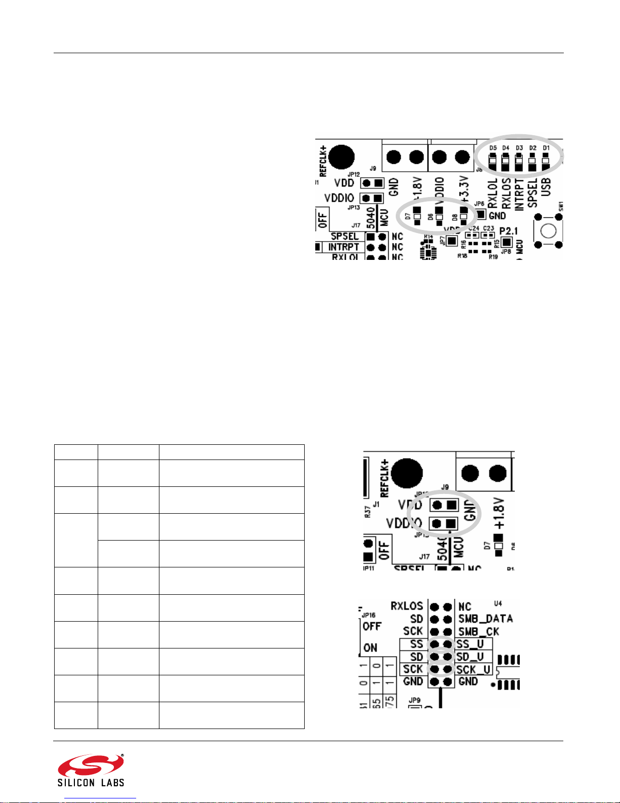
1.1. Input Power
This evaluation board requires three power inputs,
+1.8 V, +3.3 V, and V
ground connection. J8 and J9 are used for connecting
power to the EVB (see Figure 1).
1.2. LEDs
Three LEDs indicate that power has been properly
applied to the EVB. These are +3.3 V, V
+1.8 V. Since these LEDs are driven by the MCU (not
the power itself), the V
function unless +3.3 V is first applied to the EVB (see
Figure 1).
The 3.3 V LED will be on solid when the 3.3 V input is
within the 2.97 to 3.63 V range. The 1.8 V LED will be
on solid when the 1.8 V at the Si5040 V
the 1.62 to 1.89 V range.
The V
is between 1.89 and 3.63 V. The V
and off when this voltage is between 1.62 and 1.8 9 V.
The REF ON LED indicates that the Si534 clock
reference chip is powered up and applying a clock
signal to the Si5040. JP16 must be set to the ON
position in order to power up the Si534.
LED Status Description
3.3 V ON
1.8 V ON
VDDIO
REF
ON
USB ON
SPSEL ON
INTRPT ON
RXLOS ON
RXLOL ON
LED will be on solid when this input voltage
DDIO
Table 1. LED Status and Description
ON
FLASHING
ON
(1.8 V or 3.3 V), as well as a
DDIO
DDIO
and +1.8 V LEDs will not
DDIO
pins is within
DD
LED will flash on
DDIO
When 3.3 V supply is between
2.97 and 3.63 V.
When Si5040 V
pins are
DD
between 1.62 and 1.89 V.
When Si5040 V
DDIO
pin is
between 1.89 and 3.63 V.
When Si5040 V
DDIO
pin is
between 1.62 and 1.89 V.
When the Reference clock
source Si534 is powered up.
Flashes when USB Access is
occurring.
When the Si5040 SPSEL pin is
high.
When the Si5040 INTRPT pin
is high.
When the Si5040 RXLOS pin
is high.
When the Si5040 RXLOL pin is
high.
, and
Since the 1.8 V LED indicates the voltage at the Si5040
V
pins, the jumper, JP12, must be in place for this
DD
LED to function and for the Si5040 to receive its core
supply voltage. However, the V
LED will function
DDIO
without the jumper on JP13.
Figure 1. LED
1.3. Jumpers and Headers
For the EVB to function, there are five jumpers that
must be installed.
There must be jumpers on JP12 and JP13 because
they apply power to the Si5040 (see Figure 2). The next
three required jumpers are three positions on J17,
labeled SS, SD, and SCK on one side and SS_U,
SD_U, and SCK_U on the other side (see Figure 3).
Connecting jumpers between SS to SS_U, SD to SD_U,
and SCK to SCK_U enables the onboard MCU to
communicate with the Si5040 using the 3-wire serial
interface.
Figure 2. JP12 and JP13
Figure 3. J17
Rev. 0.4 3
Si5040-EVB
1.3.1. MCU to Si5040 Serial Communications
(Status and Control)
The microcode within the MCU is designed to
communicate with the Si5040 when SPSEL pin 9 is high
(JP11 no jumper). In this mode, the serial data transfer
from the MCU to the Si5040 is very similar to the SPI
protocol but with a single bidirectional data line rather
than two unidirectional data lines. However, one could
write new microcode for the MCU that uses the SMBus
2
(I
C compatible) to communicate with the Si5040. To
enable SMBus communication between the Si5040 and
the MCU, you must install a jumper on JP11 and on J17
between SD/SMB_DAT, SCK/SMB_CK and SS/SS_U.
See Figure 4. Note that INTRPT on JP17 should be
labeled as INTRPTB because the interrupt from the
Si5040 is an active low signal.
Figure 5. External MCU
1.3.3. Reference Clock
To use the on-chip reference c lock (Si534), JP16 must
be set to the ON position. When this is done, the REF
ON LED will light, indicating that power is applied to the
Si534. The output frequency of the Si534 is controlled
by jumpers JP17 and JP18 (see Figure 6).
Figure 4. SMBus Protocol
1.3.2. External MCU Control
To use an external MCU, make sure that all jumpers are
removed from J17 and that JP11 does not have a
jumper (see Figure 5). Now, the following pins of J17
are available for connection to an external MCU.
SCK
SD
SS
RXLOS
RXLOL
INTRPT
SPSEL
GND
The Silicon Labs MCU that is well-suited for use within
XFP Modules is the C8051F330.
Figure 6. Reference Clock
1.3.4. Synchronous Test Clock
By setting Register 57 to 9Ch, the Tx CMU clock divided
by 64 will be output at J2 and J3. The EVB must have
jumpers on JP2 and JP3 to enable the /64 clock output
(see Figure 7). By setting Register 57 to 1Ch, the Rx
CMU clock divided by 64 will be output at J2 and J3.
When jumpers are placed on JP2 and JP3, the
functionality of RXLOS and RXLOL is lost, and the state
of the LEDs for these two signals becomes invalid. To
return the RXLOL and RXLOS signals to their normal
modes, set Register 57 to 00h, and remove the jumpers
on JP2 and JP3. Register 57 cannot be changed with
the System Programmer GUI, you must use the
Register Programmer GUI (see page 8).
4 Rev. 0.4
Figure 7. Synchronous Test Clock
1.4. Reference Clock Details
The Si5040 can function without a reference clock and
meet all system jitter generation and jitter tolerance
specifications. However, the presence of a reference
clock provides the following capabilities:
Ability to mea su re the freq ue n cy er ro r of th e inp ut
data and generate a Loss-of-Lock indication if the
frequency error exceeds 1000 ppm with respect to
the reference clock.
Only acquire lock if the input data is within 200 ppm.
If the reference clock is synchronous, the Si5040
can operate in the clean, synchronous CMU mode
as defined in section 3.9.1 of the XFP specificatio n.
A reference clock to the Si5040 can be input from an
external source, or it can be generated from the
onboard Si534. Since the clock from the Si534 is
linearly summed with the external reference clock input,
care must be taken to ensure that both clock sources
are not active at the same time. When the Si534 is
enabled (JP16 on), its output will be present at SMAs J1
and J5 for monitoring and/or system usage. When the
Si534 is OFF, a differential clock applied at J1 and J5
will be attenuated by 2.7 dB before it reaches the
REFCLK± inputs of the Si5040.
While an Si534 has the capability of generating any four
frequencies between 10 MHz and 1400 MHz, this Si534
has been programmed to generate four specific
frequencies. Jumpers JP17 and JP18 control the
FS[1:0] inputs to the Si534 (see Figure 6). The four
frequencies are as follows:
155.52000 MHz Set FS[1:0] = 00
This is 1/64 of the SONET OC-192 rate of
9.95328e9 bps
161.13281 MHz Set FS[1:0] = 01
This is 1/64 of the 10 GIGE LAN PHY rate of
10.3125e9 bps
Si5040-EVB
167.33165 MHz Set FS[1:0] = 10
This is 1/64 of the SONET OC-192 rate with 255/237
FEC overhead (10.709225e9 bps)
173.37075 MHz Set FS[1:0] = 11
This is 1/64 of the 10 GIGE LAN Phy rate with 255/
237 FEC overhead (11.095727e9 bps)
The Si534 holds the above frequencies to within
±20 ppm over temperature (–40 to +85 °C) and voltage.
The XFP specification allows for an optional clean
synchronous CMU mode if the reference clock has
sufficiently low phase noise. See Section 3.9.1 and
Table 25 of the XFP specification. For the four
frequencies above, the typical phase noise of the Si534
is shown in Table 2 with the XFP requirements for
reference.
Table 2. Phase Noise
Frequency
Offset
1 kHz –116 dBc/Hz –85 dBc
10 kHz –120 dBc/Hz –108 dBc
100 kHz –128 dBc/Hz –128 dBc
1 M Hz –141 dBc/Hz –138 dBc
10 MHz –144 dBc/Hz –138 dBc
1.5. Crystal Cleaning
There is a crystal, Y1, on the evaluation board that is
located very close to the Si5040 for the purpose of jitter
improvement on the Txdout signal. Y1 is a 114.285 Mhz
third overtone crystal that is enabled by putting the
transmit CMU into crystal cleaning Mode 3. Even when
the Si5040 uses the crystal for transmit jitter
improvement, the transmit CMU is still continuously
agile across the entire operating range of 9.9 to
11.4 GHz. Of course, the transmit CMU may also
operate without the Y1 crystal and still be continuously
rate agile (mode 0). The layout for Y1 is specifically
designed for three different size crystals, 3.5x6 mm,
3.2x5 mm, and 2.5x3.2 mm.
1.6. RD Preemphasis
Even though the output data at the Si5040 RD pins has
very fast transitions, we have found that some
customers prefer some signal shaping of the RD output
signal at the XFI. Therefore, the Si5040 EVB that you
are receiving has a pre-emphasis circuit added to the
RD± outputs. This circuit is composed of a few resistors
and capacitors, all of which can be generic, low-cost
units. Because it is a passive circuit, it slightly
Si534 Nominal
Performance
XFP Clean
Synch CMU
Specification
Rev. 0.4 5
Si5040-EVB
20.5
3.0 pF
5040
RD+
XFI RD+
274
.01 uF
20.5
3.0 pF
5040
RD-
274
.01 µF
XFI RD-
20.5
3.0 pf
5040 RD+
XFI RD+
20.5
3.0 pf
5040 RD-
274
XFI RD-
.01 µ F
274
attenuates the RD signal, which requires that the RD
signal level from the Si5040 be slightly increased.
Please use the Si5040 Register 56 to increase the RD
drive signal from its default value of 600 mV to either
700 or 800 mV. See the Si5040 datasheet for more
information. The circuit that is implemented on the EVB
is shown below:
Figure 8. EVB Pre-Emphasis Circuit
Within an XFP module, the pre-emphasis circuit should
be located as close to the Si5040 RD± pins as is
practical. In an XFP module, the pre-emphasis circuit
above can be modified to remove one component yet
still behave the same electrically. The following circuit
shows this simplification.
1.7. Start Up Script(s)
1.7.1. For Evaluation Boards Populated with the
Rev. A Device
It is necessary to load the scripts included with the
evaluation board software at startup and after any reset
of the Si5040 Rev A. The default name for the initialization
script is "Si5040InitialRegisterMapSettings.txt". This
script will set up the Rev A device in Mode 0, the
Reference-less operation mode.
If you need to set up the Rev A device in Mode 3, the
jitter attenuation mode with external crystal
"Mode3OvtInit.txt" script needs to be loaded after
"Si5040InitialRegisterMapSettings.txt" is first loaded.
Note that these scripts should be loaded by using the
Register Programmer. See "2.5. Si5040 EVB Software
Description" on page 8 for more information on the
Register Programmer.
1.7.2. For Evaluation Boards Populated with the
Rev. B Device
Starting Oct 2006, no initialization script is required for
Mode 0 operation. However, in order for the interrupt pin
to function properly on the evaluation board, Register 2
needs to be set to 18h (default=58h) by using the
Register Programmer. Note that this is to set the
interrupt output driver as CMOS as the evaluation board
does not have an external pullup on the interrupt signal.
If you need to set up the Rev B device in Mode 3,
Register 134 needs to be set to 3h (default=30h) by
using the Register Programmer, or simply go to System
Programmer and click on the TX CDR/CMU Control link
in the block diagram. Then, choose "Mode 3" from the
"cmuMode" pull-down menu.
Figure 9. Recommended XFP Pre-Emphasis Circuit
Should you not like the eye pattern at the RD± pins, this
circuit can be easily optimized for your application. If
you wish assistance in this matter, please contact Siicon
Laboratories.
6 Rev. 0.4

Si5040-EVB
2. EVB Software Installation
The following sections describe how to install the EVB
software.
2.1. PC System Requirements
Microsoft Windows 2000 or Windows XP
USB 2.0
2 MB of hard drive space
1024x768 screen resolution or greater (1280 x 1024
recommended)
Microsoft .NET Framework 1.1
Si5040 EVB Driver
Note: The Si5040 EVB driver is provided with the installation
files.
2.2. Microsoft .NET Framework Installation
The Microsoft .NET Framework is required before
installing and running the Si5040 software. Details and
installation information about the .NET Framework are
available via a shortcut in the NETFramework directory
or at the following web site:
http://www.microsoft.com/downloads/
details.aspx?FamilyId=262D25E3-F589-4842-8157034D1E7CF3A3&displaylang=en
Contact your system administrator for more details.
2.3. Si5040 EVB Driver
The Si5040 evaluation board requires a driver to be
controlled by the software. The following section lists
the steps for installing and uninstalling the driver.
2.3.1. Install
The driver files must be installed before the EVB is
connected to the PC via the USB cable. This installation
usually only needs to be completed once per PC.
1. Navigate to the “Si5040EVBDriver” directory.
2. Double-click on the PreInstaller.exe file to run the
installation program for the driver.
3. Click Install in the dialog box. Be sure to select a
location on the PC’s hard drive for the files, if
necessary.
4. If the PC is running Windows XP, click Continue
Anyway when the wizard warns that the driver does
not pass the Windows Logo verification for XP.
After the above files are installed, the operating system
will be able to identify the EVB’s USB controller when
the EVB is connected to the PC. The following steps
occur when the EVB is connected to the PC for the first
time.
For Windows 2000, when the EVB is connected to the
PC, the operating system will display a dialog box
indicating that it found new hardware. No other action is
required. The driver installation can be verified in the
Device Manager under the USB section; look for
“Si5040EVB” in the list.
For Windows XP:
1. When the EVB is connected to the PC, the Found
New Hardware wizard will appear. Use the default
settings that will tell the PC to look for the driver.
2. Again, ignore the warning about the driver not
passing verification by clicking Continue Anyway.
3. Click Finish to complete the install.
2.3.2. Uninstall
In the Control Panel, select Add/Remove Programs.
Then select “Si5040EVB Driver Set” and click Change/
Remove. The wizard will remove the necessary files.
2.4. Si5040 EVB Software Installation
To install:
1. Navigate to the “Si5040Software” directory.
2. Double-click on the Setup.exe
3. Follow the steps in the wizard to install the program.
Note: Use the default installation location for best results.
4. After the installation is complete, click on Start
ProgramsSilicon LaboratoriesSi5040
Software. Select one of the Si5040 programs to
control the EVB.
5. Refer to the online help in each program by clicking
HelpHelp.
To uninstall:
1. Open Add/Remove Programs in the Control Panel.
2. Select the Si5040 Software, and click Remove.
3. Follow the steps in the wizard to complete the
removal.
Rev. 0.4 7

Si5040-EVB
2.5. Si5040 EVB Software Description
There are three programs to control the Si5040. Each
provides a different kind of access to th e device. Refer
to the online help in each program by clicking
Help
Help in the menu for more inform atio n on how to
use the software.
Program Description
The Register Viewer displays the current data in a table format sorted by
Register
Viewer
Register
Programmer
register address of the Si5040 register
map to provide a quick view of the
Si5040’s state. This program can save
and print the register map.
The Register Programmer provides
low-level register control of the
Si5040. Single and batch operations
are provided to read from and write to
the device. Register map files can be
saved and opened in the batch mode.
System
Programmer
The Si5040 System Programmer provides high-level control of the Si5040.
There are multiple settings for this
chip; so, this program will make it easier to configure these settings. (The
settings this program can control are
documented in the Si5040 data sheet.)
The software can also save and open
the register data in a text file format.
8 Rev. 0.4
 Loading...