

Page 1

AN692
Si4355/Si4455 PROGRAMMING GUIDE
1. Introduction
This document provides an overview of how to configure and control the following EZRadio® chips:
Si4455 transceiver
Si4355 receiver
The following code examples are covered in this programming guide:
How to set up a continuous wave (CW) transmission.
How to set up a pseudo random (PN9) transmission.
How to transmit in TX direct mode.
How to receive in RX direct mode (for BER measurement).
How to transmit a simple packet in Packet Handler mode.
How to receive a simple packet in Packet Handler mode.
How to implement bidirectional variable length packet based communication.
2. Hardware Options
The source code is provided for two different hardware platforms:
RFStick
Wireless Motherboard + RF Pico Board
A separate Silicon Labs IDE workspace is provided for each example on the two platforms.
2.1. The RFStick Platform
Figure 1. RFStick
The RFStick is a basic demo system for the evaluation of the EZRadio chips. The board has two main parts, the
MCU part and the radio part. The MCU part of the board contains a Silicon Labs C8051F930 MCU and basic
human interface devices (four push-buttons, four LEDs, four switches and a buzzer). The radio part contains the
EZRadio chip, the matching circuit, and the antenna. The RF output is selectable via a 0 resistor between a PCB
antenna and an optional (unpopulated) 50 SMA output connector. The MCU is connected to the EZRadio chip
via an SPI bus and some other GPIOs (see Table 1). The RF section of the board can be broken off along a
perforation between the two rows of J3 and installed in the user’s own hardware as a radio module by utilizing the
remaining row of J3.
Table 1 contains the signal connections between the EZRadio chip and the MCU:
Rev 0.4 11/14 Copyright © 2014 by Silicon Laboratories AN692
Page 2

AN692
Table 1. Connections between the EZRadio Chip and the MCU
Si4355, Si4455 RFStick C80C51F930
Pin Number Pin Name Pin Function Connections
across J3
EP, 1, 6, 9 GND Ground 3–4 GND GND
7, 8 VDD Supply Voltage input 1–2 VDD VDD
12 NIRQ
2 SDN
16 NSEL SPI select input 11–12 NSEL P1.3
13 SCLK SPI clock input 17–18 SCLK P1.0
15 SDI SPI data input 13–14 MOSI P1.2
14 SDO SPI data output 15–16 MISO P1.1
10 GPIO_0 General Purpose I/O 23 x 24 GPIO_0/PB1 P0.0
11 GPIO_1 General Purpose I/O 21 x 22 GPIO_1/PB2 P0.1
19 GPIO_2 General Purpose I/O 9 x 10 GPIO_2/PB3 P0.2
20 GPIO_3 General Purpose I/O 7 x 8 GPIO_3/PB4 P0.3
Interrupt output,
active low
Shutdown input,
active high
19–20 NIRQ P1.4
5–6 SDN P1.5
Signal Name Pin Name
The four GPIO signals’ primary function is push button input to the MCU (PB1–PB4), so these signals are not
connected to the EZRadio chip by default (represented by x in Table 1). The user can connect them by soldering in
jumpers across the appropriate pins of J3.
2 Rev 0.4
Page 3

AN692
2.1.1. Setting up and Connecting the RFStick to a PC
The power source of the board can be selected with the power-supply selector switch (S6). If S6 is in the Adapter
position, supply voltage is provided by a Toolstick Base Adapter that is connected to the J1 PCB edge connector. If
S6 is in the Battery position, the supply voltage is provided by two AAA batteries in the battery holder on the bottom
side of the board. Current consumption of the RF part (RFVDD) can be measured on J6. Since J6 is shorted by a
PCB track on the bottom side of the board, the user must cut the track if this feature is used.
Figure 2. How to Connect the RFStick to the PC
Steps for connecting to a PC:
Select the desired power source with S6 power selector switch.
Connect the J1 connector of the RFStick to the Toolstick Base Adapter.
Connect the Toolstick Base Adapter to the USB port of the PC.
Wait for Windows to install the driver of the Toolstick Base Adapter, if necessary.
The RFStick is available in three different frequency band versions from Silicon Labs as part of several EZRadio
kits (i.e., 434, 868, and 915 MHz).
Rev 0.4 3
Page 4

AN692
2.2. The Wireless Motherboard Platform
The Wireless Motherboard (WMB) platform is a demo and development platform for the EZRadio and
EZRadioPRO radio ICs. It consists of a Wireless Motherboard and interchangeable MCU Pico Boards and RF Pico
Boards.
Figure 3. Wireless Motherboard Platform
Table 2. . Kits that Contain the Wireless Motherboard Platform
Part Number Kit Name
EZR-LCDK2W-434 EZRadio Two Way Link Development Kit 434 MHz
EZR-LCDK2W-868 EZRadio Two Way Link Development Kit 868 MHz
EZR-LCDK2W-915 EZRadio Two Way Link Development Kit 915 MHz
4012-LCDK1W-434 Si4012 EZRadio One Way Link Development Kit 434 MHz
4012-LCDK1W-915 Si4012 EZRadio One Way Link Development Kit 915 MHz
4 Rev 0.4
Page 5

2.2.1. The Wireless Motherboard
AN692
Figure 4. Wireless Motherboard
The wireless motherboard contains four pushbuttons, four LEDs, and a buzzer as simple user interfaces. A
graphical LCD displays menu items for range testing purposes and a potentiometer demonstrates analog
capabilities of the MCU. A switch supports the power options of the MCU's built-in dc/dc converter. Using the
current measurement jumpers, current consumption can be measured separately either for the MCU, the radio, or
the peripherals. The motherboard contains test pins for all I/O pins of the MCU and for all digital pins of the radio. In
addition, there are SMA connectors for the GPIOs of the radio for test equipment connection. A USB
communication interface as well as a built-in Silicon Labs USB-to-C2 debug adapter are integrated onto the board
so that the wireless motherboard (WMB) can be directly connected via USB to the PC for downloading and
debugging code on the MCU.
The WMB also contains an interface connection to sensor modules. The RF pico boards can be connected to the
WMB through a connector pair.
Rev 0.4 5
Page 6

AN692
2.2.2. Power Scheme
The power source of the platform can be selected with the power supply selector switch “SUPPLY SELECT” on the
WMB board. If this switch is in the ”USB” position, supply voltage is provided by the PC that is connected to the
”J16” mini USB connector. If this switch is in the ”BAT” position, the supply voltage is provided by two AA batteries
in the battery holder on the bottom side of the board. If the ”SUPPLY SELECT” switch is in the ”EXT” position,
supply voltage is provided by an external power source through the ”TP7” and “TP9” points.
Using the ”MCU dc/dc” switch, the internal dc/dc converter of the C88051F930 MCU on the MCU pico board can
be activated if the connected pico board supports this function. If the switch is in ”OFF” position, the MCU's dc/dc
converter is inactive and the supply voltage is only determined by the state of the “SUPPLY SELECT” switch.
Positioning the switch to either ”LDO (1.25 V)” or ”1 CELL” position will turn on the MCU's dc/dc converter by
connecting 1.25–1.5 V supply voltage to the VBAT pin and removing external power from the VDC pin. The MCU
will provide 1.9 V in default setting on its VDC pin to all the other connected loads. Since this current is limited, it
may be necessary to disconnect or disable some loading part of the board. For further details, see the MCU data
sheet and the board schematic. The board schematic can be found in the EZRadioPRO Development Kit User's
Guide. A complete CAD design pack of the board is also available at www.silabs.com.
2.2.3. RF Pico Board
Figure 5. RF Pico Board
The RF Pico Board is a radio module that contains an EZRadio IC, matching network, and pcb antenna. The RF
output is a 50 SMA output connector. The boards also have a factory loaded board identification memory (EBID)
that contains data that describes the board properties. Via the unified RF pico connector pair on the bottom side of
the board, any RF pico board can be connected to the WMB.
2.2.4. Setting up and Connecting the WMB to the PC
Steps for connecting the platform to the PC:
1. Connect an RF Pico Board to the WMB board through the CON1 and CON2 connectors.
2. Insert a UPPI-930-RF MCU pico board in the connectors J5, J6, J7, J8 on the WMB. The dotted corner of
the C8051F930 MCU has to point to the triangle symbol on the WMB.
3. Connect an antenna to the SMA connector on the RF Pico Board.
4. Select the desired power source with the SUPPLY SELECT switch.
5. Ensure that all the CURRENT MEASUREMENT jumpers are in place.
6. Connect the WMB board to a USB port of the PC.
7. Wait for Windows to install the driver of the debug interface if necessary.
6 Rev 0.4
Page 7

AN692
3. Software Tools
Two software tools are provided by Silicon Labs to help EZRadio software development, the Wireless Development
Suite (WDS) and the Silicon Labs Integrated Development Environment (IDE), both available atwww.silabs.com.
3.1. Wireless Development Suite (WDS)
The recommended starting point for Si4355/4455 development is the WDS. It can be downloaded from
www.silabs.com.and can be installed on a PC. After connecting one of the hardware platforms described in this
document to the PC, WDS is able to identify the connected board by reading the EBID memories.
The Radio Configuration Application GUI is part of the WDS program. This setup interface provides an easy path to
quickly selecting and loading the desired configuration for the Si4355/4455 device. After the desired configuration
is selected, the EZConfig setup automatically creates the configuration data that can be used to configure the
EZRadio chip. The program then gives the option to directly configure the EZRadio chip of the connected
hardware, to modify a selected example code with the configuration and download it to the connected hardware, or
to launch Silicon Labs IDE with the new configuration data preloaded into the selected example project. For more
information on WDS and EZConfig usage, refer to the application notes “AN796: Wireless Development Suite
General Description” and “AN797: WDS User’s Guide for EZRadio Devices”, available at www.silabs.com.
Rev 0.4 7
Page 8

AN692
Figure 6. Device Configuration Options
8 Rev 0.4
Page 9

AN692
3.2. Silicon Labs IDE
The Silicon Laboratories Integrated Development Environment (IDE) is a standard tool for program development
for any Silicon Labs 8-bit MCUs, including the C8051F930 that is used on the hardware platforms described in this
document. The Silicon Laboratories IDE integrates a project manager, a source-code editor, source-level
debugger, and an in-system flash programmer. The IDE interfaces to third party development tool chains to provide
system designers a complete embedded software development environment. The Keil Demonstration Toolset
includes a compiler, linker, and assembler and easily integrates into the IDE.
3.2.1. Downloading and Running the Example Codes
1. Connect the hardware platform to the PC according to the description of the used platform.
2. Start Silicon Labs IDE (IDE 4.40 or higher required) on your computer.
3. Select Project→Open Project... to open a previously saved project.
4. Before connecting to the target device, several connection options may need to be set. Open the
Connection Options window by selecting Options→Connection Options... in the IDE menu.
5. Select USB Debug Adapter in the “Serial Adapter” section.
6. If more than one adapter is connected, choose the appropriate serial number from the drop-down list.
7. Check the “Power target after disconnect” if the target board is currently being powered by the USB Debug
Adapter. The board will remain powered after a software disconnect by the IDE.
8. Next, the correct “Debug Interface” must be selected. Check the C2 Debug Interface.
9. Once all the selections are made, click the OK button to close the window.
10. Click the Connect button in the toolbar or select Debug→Connect from the menu to connect to the
C8051F930 MCU of the platform.
11. Erase the flash of the C8051F930 MCU in the Debug→Download object code→ Erase all code space
menu item.
12. Download the desired example HEX file either by hitting the Download code (Alt+D) toolbar button or from
the Debug →Download object code menu item.
13. Hit the Disconnect toolbar button or invoke the Debug →Disconnect menu item to release the device from
halt and to let it run.
Rev 0.4 9
Page 10

AN692
3.3. ToolStick Terminal
The ToolStick Terminal program provides the standard terminal interface to the target microcontroller's UART.
However, instead of requiring the usual RS-232 and COM port connection, ToolStick Terminal uses the USB
interface of the ToolStick Base Adapter to provide the same functionality. The firmware on the target microcontroller
does not need to be customized to use the UART and communicate with ToolStick Terminal. The firmware on the
microcontroller should write to the UART as it would in any standard application and all of the translation is handled
by the ToolStick Base Adapter.
The ToolStick Base Adapter is integrated on the WMB and is also part of the RFStick platform as a separate
device.
The ToolStick Terminal program is part of the Silicon Labs IDE and is also available as a separate application. Both
can be installed as part of the Silicon Labs 8-bit Microcontroller Studio from:
http://www.silabs.com/products/mcu/Pages/8-bit-microcontroller-software.aspx
The IDE and its built in ToolStick Terminal can communicate with the target MCU simultaneously on the C2
interface and on the UART respectively.
To use the ToolStick Terminal in the IDE (above v4.60.00), follow these steps:
1. Open the Silabs IDE from the Start Programs Silicon Laboratories menu.
2. Go to the OptionsConnection Options menu and select the desired ToolStick Base Adapter from the drop
down list.
3. Click on the Connect button to connect the IDE to the target MCU via the C2 interface.
4. From the Tools menu, start the Toolstick Terminal. In the top left-hand corner of the Terminal application, go
to the ToolStickSettings menu and set the communication parameters. Now the ToolStick Terminal is
ready for use. In the "Receive Data" window, text indicating the received characters will appear.
In addition to the standard two UART pins (TX and RX), there are two GPIO/UART handshaking pins on the
ToolStick Base Adapter. On both the WMB and RFStick platforms GPIO0 is used for the internal purpose of the
WDS to select between the C2 interface of the target MCU and the EBID MCU. GPIO1 is not connected. Although
the separate ToolStick Terminal application provides the functionality to control these GPIOs, default settings for
GPIO0 should not be changed.
10 Rev 0.4
Page 11

AN692
4. Using the Si4355/Si4455 Radios
Si4355 and Si4455 are easy-to-use radio chips that combine plug-and-play simplicity with the flexibility needed to
handle a wide variety of applications. This chapter describes how to operate the Si4355/Si4455 radios.
4.1. Radio Hardware Interface
The Si4355/Si4455 radios have several pins to interface to a host MCU. Four pins, SDI, SDO, SCLK, NSEL, are
used to control the radio over the SPI bus. The user has access to an Application Programming Interface (API) via
the SPI bus, which is described in section “4.2. Application Programming Interface”. The Shutdown (SDN) pin is
used to completely disable the radio (when the pin is pulled high) and put the device into the lowest power
consumption state. After the SDN pin is pulled low, the radio wakes up and performs a Power On Reset. It takes
about 1 ms until the chip is ready to receive commands on the SPI bus (GPIO1 pin goes high when the radio is
ready for receiving SPI commands). When SDN is high and the radio is in shutdown state, the GPIOs are set to
drive an output low level. The radio has an interrupt output pin, NIRQ, which can be used to promptly notify the
host MCU of various events. The NIRQ pin is active low, and goes back to high if the pending interrupt flag was
cleared by reading the appropriate Interrupt Pending registers.
Table 3. Serial Peripheral Interface Signals
Radio Pin Signal Description
SCLK Serial Clock Output From Master
SDI Master Output, Slave Input
SDO Master Input, Slave Output
NSEL Slave Select, Active Low
Figure 7. Connections between the Radio Chip and the Host Microcontroller
Rev 0.4 11
Page 12

AN692
4.2. Application Programming Interface
The programming interface allows the user to do the following:
Send commands to the radio.
Read status information.
Set and get radio parameters.
Handle the Transmit and Receive FIFOs.
The API commands are listed in the following table:
Table 4. List of the Radio API Commands
Command ID Radio API Command Description
0x00 NOP No operation command
0x02 POWER_UP
0x01 PART_INFO Reports basic information about the device
0x10 FUNC_INFO Returns the function revision information of the device
0x11 SET_PROPERTY Sets the value of a property
0x12 GET_PROPERTY Retrieves a property's value
0x13 GPIO_PIN_CFG Configures the GPIO pins
0x15 FIFO_INFO
0x19 EZCONFIG_CHECK Validates the EZConfig array was written correctly
0x20 GET_INT_STATUS Returns the interrupt status byte
0x31 START_TX
0x32 START_RX Switches to RX state
0x33 REQUEST_DEVICE_STATE Request current device state
0x34 CHANGE_STATE Update state machine entries
0x44 READ_CMD_BUFF
0x50 FRR_A_READ
0x51 FRR_B_READ
0x53 FRR_C_READ
0x57 FRR_D_READ
0x66 EZCONFIG_SETUP Configures device using EZConfig array
0x66 WRITE_TX_FIFO Writes TX data buffer (max. 64 bytes, Si4455 only)
0x77 READ_RX_FIFO Reads RX data buffer (max. 64 bytes)
Powerup device and mode selection. Modes include operational function
Provides access to transmit and receive FIFO counts and
reset
Switches to TX state and starts packet transmission
(Si4455only)
Returns Clear to Send (CTS) value and the result of the previous command
Reads the fast response registers (FRR) starting with
FRR_A.
Reads the fast response registers (FRR) starting with
FRR_B.
Reads the fast response registers (FRR) starting with
FRR_C.
Reads the fast response registers (FRR) starting with
FRR_D.
12 Rev 0.4
Page 13

The API properties are listed in Table 5.
Table 5. List of the Radio API Properties
AN692
Property
Group
0x01 0x00 INT_CTL_ENABLE Interrupt enable property 0x04
0x01 0x01 INT_CTL_PH_ENABLE Packet handler interrupt enable property 0x00
0x01 0x02 INT_CTL_MODEM_ENABLE Modem interrupt enable property 0x00
0x01 0x03 INT_CTL_CHIP_ENABLE Chip interrupt enable property 0x04
0x02 0x00 FRR_CTL_A_MODE Fast Response Register A Configuration 0x01
0x02 0x01 FRR_CTL_B_MODE Fast Response Register B Configuration 0x02
0x02 0x02 FRR_CTL_C_MODE Fast Response Register C Configuration 0x09
0x02 0x03 FRR_CTL_D_MODE Fast Response Register D Configuration 0x00
0x22 0x01 PA_PWR_LVL PA Level Configuration 0x7F
0x24 0x03 EZCONFIG_XO_TUNE
0x40 0x00 FREQ_CONTROL_INTE Frac-N PLL integer number 0x3C
0x40 0x01 FREQ_CONTROL_FRAC_2 Byte 2 of Frac-N PLL fraction number 0x08
Number Name Description Default
Configure crystal oscillator frequency tuning
bank
0x40
0x40 0x02 FREQ_CONTROL_FRAC_1 Byte 1 of Frac-N PLL fraction number 0x08
0x40 0x03 FREQ_CONTROL_FRAC_0 Byte 0 of Frac-N PLL fraction number 0x08
0x40 0x04
0x40 0x05
The following sections describe the SPI transactions of sending commands and getting information from the chip.
4.2.1. Sending Commands to a Radio
The behavior of the radio can be changed by sending API commands to the radio (e.g., changing the power states,
start packet transmission, etc.). The radio can be configured through several "properties". The properties represent
radio configuration settings, such as interrupt settings, modem parameters, packet handler settings, etc., and can
be set and read via API commands. For most of the commands, the host MCU does not expect any response from
the radio chip. Other commands are used to read back a property from the chip, such as checking the interrupt
status flags, reading the transmit/receive FIFOs.
After the radio receives a command, it processes the request. During this time, the radio is not capable of receiving
a new command. The host MCU must identify when the next command can be sent. The Clear to Send (CTS)
signal shows the actual status of the command buffer of the radio. It can be monitored over the SPI or on GPIOs, or
the chip can generate an interrupt if it is ready to receive the next command. These three options are detailed
below.
FREQ_CONTROL_CHANNEL_-
STEP_SIZE_1
FREQ_CONTROL_CHANNEL_-
STEP_SIZE_0
Byte 1 of channel step size
Byte 0 of channel step size
0x00
0x00
Rev 0.4 13
Page 14

AN692
4.2.2. Checking that the Radio is Ready to Receive Commands
4.2.2.1. Software Polling Method
To ensure the radio is ready to receive the next command, the host MCU must pull down the NSEL pin to monitor
the status of CTS over the SPI port. The 0x44 command ID has to be sent, and eight clock pulses have to be
generated, on the SCLK pin. During the additional eight clock cycles, the radio clocks out the CTS as a byte on the
SDO pin. When completed, the NSEL should be pulled back to high. If the CTS byte is 0xFF, then the radio
processed the last command successfully and is ready to receive the next command; in any other case, the CTS
read procedure has to be repeated from the beginning as long as the CTS byte is not 0xFF.
Figure 8. Polling the Radio Availability
4.2.2.2. GPIO Checking Method
Any GPIO can be configured for monitoring the CTS. GPIOs can be configured to go either high or low when the
chip completes the command. The function of the GPIOs can be changed by the GPIO_PIN_CFG command. By
default, GPIO1 is set as “High when command completed, low otherwise” after Power On Reset. Therefore, this pin
can be used for monitoring the CTS right after Power On Reset and to identify when the chip is ready to boot up.
4.2.2.3. NIRQ Interrupt Checking Method
The radio asserts the CHIP_READY interrupt flag if a command is completed. The interrupt flag can be monitored
by either the GET_CHIP_STATUS or the GET_INT_STATUS command. Apart from monitoring the interrupt flags,
the radio may pull down the NIRQ pin if this feature is enabled. If a new command is sent while the CTS is
asserted, then the radio ignores the new command. The Si446x can generate an interrupt to communicate this
error to the MCU by the CMD_ERROR interrupt flag in the CHIP_STATUS group. The interrupt flag has to be read
(by issuing a GET_CHIP_STATUS or GET_INTERRUPT_STATUS command) to clear the pending interrupt and
release the NIRQ pin. No other action is needed to reset the command buffer of the radio; however, after a
CMD_ERROR, the host MCU should repeat the new command after the radio has processed the previous one.
All the commands that are sent to the radio have the same structure. After pulling down the NSEL pin of the radio,
the command ID should be sent first. The commands may have up to 15 input parameters.
Figure 9. Host MCU Sends Command to Radio
14 Rev 0.4
Page 15

AN692
4.2.3. Getting a Command Response from Radio
Reading from the radio requires several steps to be followed. The host MCU should send a command with the
address it requests to read. The radio holds the CTS while it retrieves the requested information. Once the CTS is
set (0xFF), the host MCU can read the answer from the radio.
Figure 10. Read Procedure
If the CTS is polled on the GPIOs, or the radio is configured to provide interrupt if the answer is available, then the
response can be read out from the radio with the following SPI transaction:
Figure 11. Read the Response from Radio
If the CTS is polled over the SPI bus, first the host MCU should pull the NSEL pin low. This action should be
followed by sending out the 0x44 Read command ID and providing an additional eight clock pulses on the SCLK
pin. The radio will provide the CTS byte on its SDO pin during the additional clock pulses. If the CTS byte is 0x00,
then the response is not yet ready and the host MCU should pull up the NSEL pin and repeat the procedure from
the beginning as long as the CTS byte is not 0xFF. If CTS is 0xFF, then the host MCU should keep the NSEL pin
low and provide clock cycles on the SCLK pin, as many as the data to be read out requires. The radio will clock out
the requested data on its SDO pin during the additional clock pulses.
Rev 0.4 15
Page 16

AN692
Figure 12. Monitor CTS and Read the Response on the SPI Bus
Reading the response from the radio can be interrupted earlier. For example, if the host MCU asked for five bytes
of response, it may read fewer bytes in one SPI transaction. As long as a new command is not sent, the radio
keeps the response for the last request in the command buffer. The host MCU can re-read the response in a new
SPI transaction. In such a case, the response is always provided from the first byte.
Notes:
Up to 16 bytes of response can be read from the radio in one SPI transaction. If more bytes are read, the
radio will provide the same 16 bytes of response in a circular manner.
If the command has N bytes of response, but the host MCU provides less than N bytes of clock pulses
during the read sequence, it causes no issue for the radio. The response buffer is reset if a new command
is issued.
If the command has N bytes of response, but, during the read sequence, the host MCU provides more than
N bytes of clock pulses, the radio will provide unpredictable bytes after the first N bytes. The host MCU
does not need to reset the SPI interface; it happens automatically if NSEL is pulled low before the next
command is sent.
16 Rev 0.4
Page 17

AN692
4.2.4. Using Fast Response Registers
There are several types of status information that can be read out from the radio faster. The FRR_CTL_x_MODE
(where x can be A, B, C or D) properties define what status information is assigned to a given fast response
register (FRR). The actual value of the registers can be read by pulling down the NSEL pin, issuing the proper
command ID, and providing an additional eight clock pulses on the SCLK pin. During these clock pulses, the radio
provides the value of the addressed FRR. The NSEL pin has to be pulled high after finishing the register read.
Figure 13. Reading a Single Fast Response Register
It is also possible to read out multiple FRRs in a single SPI transaction. The NSEL pin has to be pulled low, and
one of the FRRs has to be addressed with the proper command ID. Providing an additional 8 x N clock cycles will
clock out an additional N number of FRRs. After the fourth byte is read, the radio will provide the value of the
registers in a circular manner. The reading stops by pulling the NSEL pin high.
Figure 14. Reading More Fast Response Registers in a Single SPI Transaction
Note: If the pending interrupt status register is read through the FRR, the NIRQ pin does not go back to high. The pending
interrupt registers have to be read by a Get response to a command sequence in order to release the NIRQ pin.
Rev 0.4 17
Page 18

AN692
4.2.5. Write and Read the FIFOs
There are two 64-byte FIFOs for RX and TX data in the Si4x55.
To fill data into the transmit FIFO, the host MCU should pull the NSEL pin low and send the 0x66 Transmit FIFO
Write command ID followed by the bytes to be filled into the FIFO. Finally, the host MCU should pull the NSEL pin
high. Up to 64 bytes can be filled into the FIFO during one SPI transaction.
Figure 15. Transmit FIFO Write
If the host MCU needs to read the receive FIFO, it has to pull the NSEL pin low and send the 0x77 Receive FIFO
Read command ID. The MCU should provide as many clock pulses on the SCLK pin as necessary for the radio to
clock out the requested amount of bytes from the FIFO on the SDO pin. Finally, the host MCU should pull up the
NSEL pin.
Figure 16. Receive FIFO Read
If more than 64 bytes are written into the Transmit FIFO, then a FIFO overflow occurs. If more bytes are read from
the Receive FIFO than it holds, then FIFO underflow occurs. In either of these cases, the
FIFO_UNDERFLOW_OVERFLOW_ERROR interrupt flag will be set. The radio can also generate an interrupt on
the NIRQ pin if this flag is enabled. The interrupt flag has to be read, by issuing a GET_CHIP_STATUS or
GET_INTERRUPT_STATUS command, to clear the pending interrupt and release the NIRQ pin.
18 Rev 0.4
Page 19

AN692
4.3. State Transitions of the EZRadio Devices
Ready state is designed to give a fast transition time to TX or RX state with reasonable current consumption. In this
mode the crystal oscillator remains enabled reducing the time required to switch to TX or RX mode by eliminating
the crystal start-up time. An automatic sequencer will put the chip into RX or TX from any state. It is not necessary
to manually step through the states. Although it is not shown in the diagram, any of the lower power states can be
returned to automatically after RX or TX.
Figure 17. Operational States and Current Consumption
Rev 0.4 19
Page 20

AN692
State/Mode Response Time to
Table 6. Switching Times between Radio States
TX RX
Shutdown 15 ms 15 ms
Sleep 440 μs 440 μs
SPI Active 340 μs 340 μs
Ready 126 μs 122 μs
TX Tune 58 μs N/A
RX Tune N/A
TX N/A
RX 130 μs 75 μs
Notes:
1. This state change is not possible in the RF chip.
2. While the chip is in sleep state, the NSEL pin has to stay in high state. If the host processor is not able to provide this
during sleep, a pullup resistor can be necessary on the NSEL pin.
1
1
74 μs
138 μs
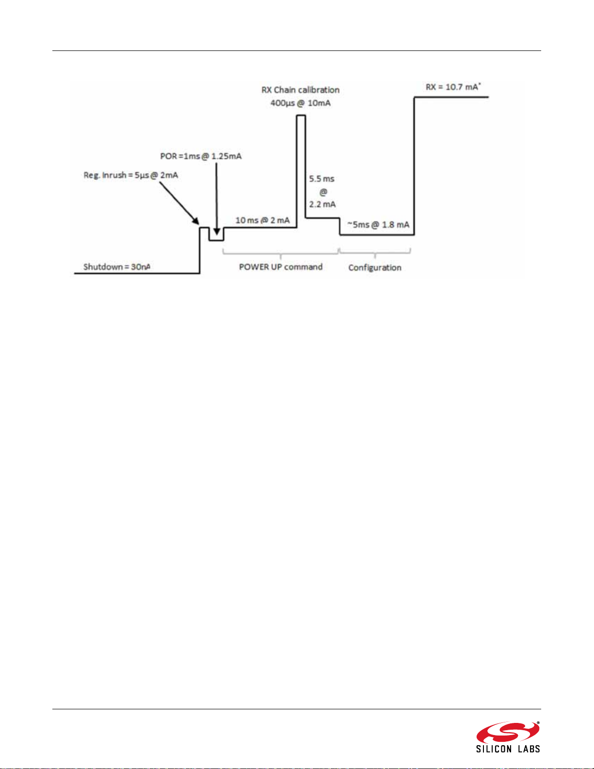
Figure 18. Supply Current versus Time Diagram from Shutdown to RF initialized Ready State
20 Rev 0.4
Page 21

AN692
Figure 19. Supply Current versus Time Diagram from Shutdown to Standby State
Figure 20. Supply Current versus Time Diagram from Shutdown to TX State
Rev 0.4 21
Page 22
AN692
Figure 21. Supply Current versus Time Diagram from Shutdown to RX State
22 Rev 0.4
Page 23
4.4. Radio Chip Waking Up
AN692
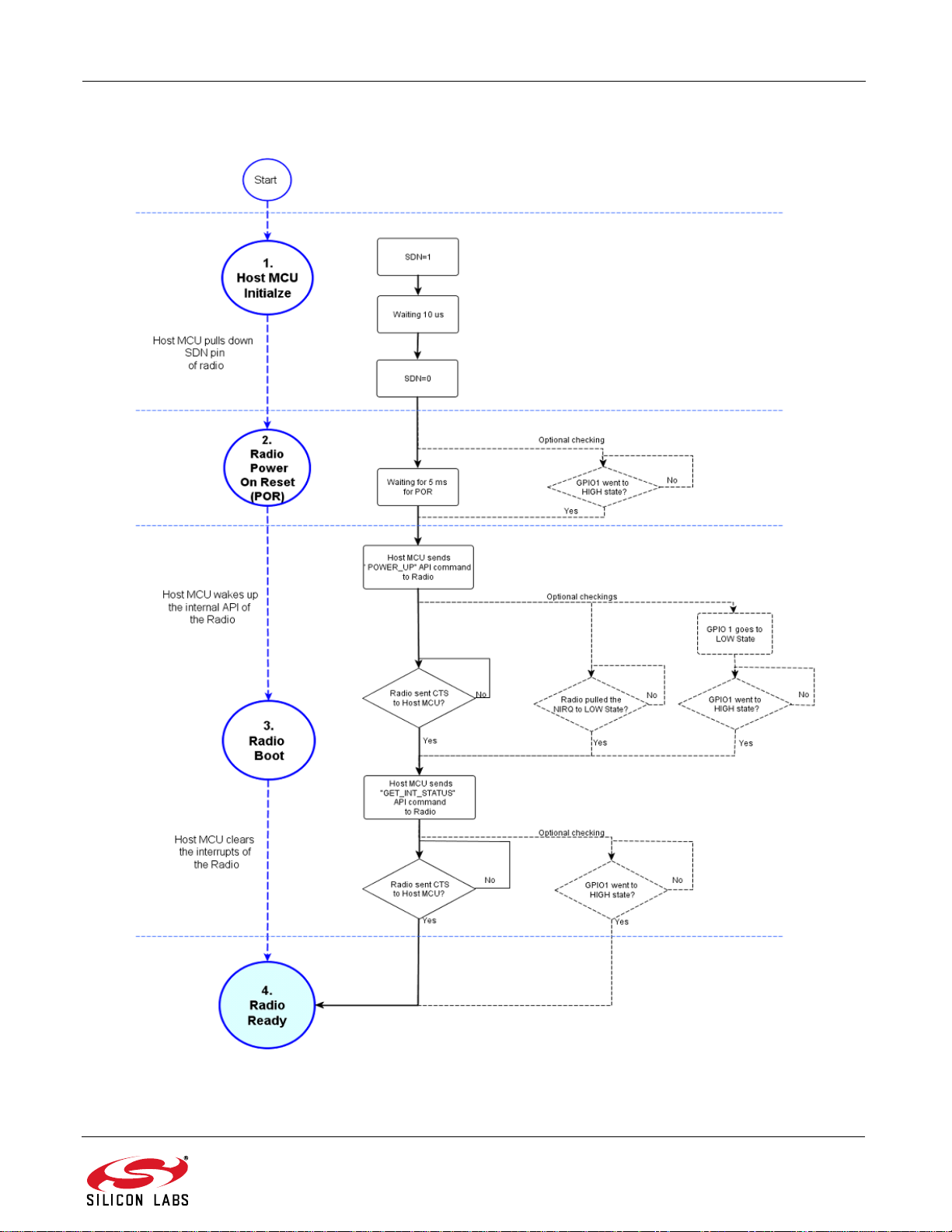
Figure 22. Radio Wake Up Process
Rev 0.4 23
Page 24

AN692
First the radio is in off state. After the SDN pin is pulled low, the radio wakes up and performs a Power on Reset,
which takes a maximum of 5 ms until the chip is ready to receive commands on the SPI bus. GPIO1 pin goes high
when the radio is ready for receiving SPI commands. During the reset period, the radio cannot accept any SPI
command.
There are two ways to determine if the chip is ready to receive SPI commands after a reset event: 1) Use a timer
in the host microcontroller to wait for this period or 2) Connect the GPIO1 pin of the radio to the host MCU and poll
the status of this pin. During the power on reset, the GPIO1 remains in low state. Once the reset is finished, the
radio sets GPIO1 to high state. Next, the radio device has to be sent to active mode by issuing a "POWER_UP"
command via the SPI interface, which takes approximately 5 ms to be completed. This process can be monitored
in three ways: The first option is to poll the CTS over the SPI; the second option is to detect that the radio pulled
down the NIRQ pin, and the third option is to detect that the radio pulled up the GPIO1 pin. Once the device is in
active mode, the host MCU must clear the interrupt flags from the radio.
24 Rev 0.4
Page 25
4.5. EZConfig and Configuration Options
AN692
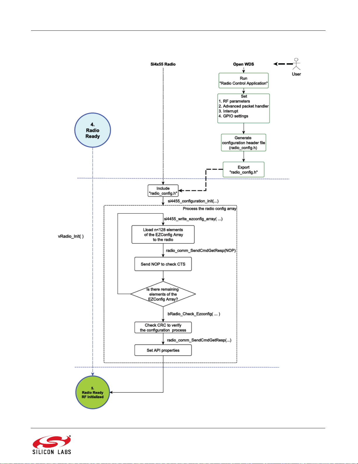
Figure 23. Radio RF Initialization Process
Rev 0.4 25
Page 26

AN692
EZConfig is a feature of Si4355/4455 that enables the customer to easily configure the radio by writing a single
configuration array into the chip upon power up, using the EZCONFIG_SETUP command of the API. Generation of
the configuration array content is automated with the Wireless Development Suite (WDS) that is provided free of
charge by Silicon Labs. The WDS saves the user from modifying hundreds of different parameters, which makes
the configuration process easy and straightforward. Based on the parameters entered into the radio configuration
application, the WDS creates the configuration data. If the Launch IDE option is selected, the WDS generates a
radio_config.h header file that contains the configuration data. This header file contains all the information needed
by the application to configure the radio properly. These are the parameters of the RF link such as the modulation
type, channel bandwidth, data rate, center frequency, crystal tolerance, crystal capacitor bank value, modulation
source, CRC calculation and sync word setting. For more information on WDS and EZConfig usage, refer to the
application notes “AN796: Wireless Development Suite General Description” and “AN797: WDS User’s Guide for
EZRadio Devices.”
After the radio chip has been woken up according to the description in the previous chapter, it needs to be
configured with the RF parameters. Using the Radio Control Application, all of the radio related parameters can be
set. On the RF parameters tab, the center carrier frequency, tolerance and frequency of the used crystal, channel
spacing, and the level of the power amplifier can be configured. On the advanced packet handler tab, the length of
the preamble and the pattern of the synchron word can be configured. Manchester coding and the CRC calculation
can be enabled or disabled. The used packet length also can be customized. In addition, the radio can provide a
clock signal through its GPIOs. On the interrupt tab, the interrupt sources of the internal modem of the chip and the
packet handler can be enabled. On the GPIO settings, the four GPIOs, the NIRQ, and the SDO pin can be
configured to one of the 19 available functions including valid preamble output or sync word detect output. Having
configured all the radio parameters, the generated "radio_config.h" header file can be exported from WDS.
Numerous built-in example projects can be opened in Silabs IDE including the newly created header file. All the
example codes can initialize the radio chip by the vRadio_Init( ) function. The header file contains a configuration
array called EZConfig Array and the initialized API properties. The radio chip cannot be used before the EZConfig
array is written into it. Note that using the same radio settings for generating the EZConfig Array does not provide
the same array contents due to the internal encryption method. These values are sent to the radio chip through the
SPI bus by the si4455_write_ezconfig_array( ) function. Since the array is bigger than the total size of the TX and
RX FIFOs, it is divided into parts. Since the EZCONFIG_SETUP command has no any reply, not even CTS, it is
necessary to send a NOP command after each EZCONFIG_SETUP command to be able to check CTS to know
that the chip is ready to receive the next command. The command defined as RF_EZCONFIG_CHECK verifies if
the EZConfig Array was downloaded correctly. The array is secured by a 16-bit CRC to avoid errors during
download. In the event of a CRC mismatch, the radio will drop the configuration array and remains in the
configuration state. The API properties are then configured one by one by the si4455_set_property( ) function.
Finally, the radio gets into ready state and the example code can start to run.
4.6. Radio Configuration File
The configuration file contains API commands to configure the radio and other settings of an example project. It is
interpreted as a C header file called "radio_config.h" that is generated by the "Radio Control Application" of the
WDS for the selected example project. The file consists of several sections.
The head section contains file and copyright info.
The "INPUT DATA" section contains as comments the RF parameter values to be set by the commands defined in
this config file. These RF parameters are derived from the requirements entered by the user in the WDS.
The "CONFIGURATION PARAMETERS" section contains value definitions to be used to set some variables of the
demo project.
The "CONFIGURATION COMMANDS" section contains the definitions of the API commands that will configure the
radio. Also, comments are added that describe the API command in detail.
Next, the "RADIO_CONFIGURATION_DATA_ARRAY" is composed from the previously defined commands
prefixed with command length bytes. Finally, a "RADIO_CONFIGURATION_DATA" structure is composed from the
"RADIO_CONFIGURATION_DATA_ARRAY" and the "CONFIGURATION PARAMETERS". This final structure will
hold all configuration information necessary for the example project.
It is recommended to change the parameters through WDS and not to edit the radio_config.h file directly.
26 Rev 0.4
Page 27

AN692
5. Example Projects
Several complete example projects are provided by Silicon Labs and can be configured and exported from the
WDS.
5.1. General Project Structure
All the example projects have a unified structure and common driver set. This section provides a brief introduction
of the structure of the example projects.
5.1.1. Prerequisites for Code Development
All the example projects have a unified structure and common driver set. This section provides a brief introduction
of the structure of the example software projects. The settings in the example project files assume that some
Silicon Labs or third party software tools are already installed on the PC where the example project is going to be
compiled. The tools that need to be installed depends on the functionality to be used. The following list contains a
complete set of such programs:
Silicon Laboratories IDE
Used to open the preconfigured project files and manage the build process.
Keil C51 v9.51+ compiler to use with the Silicon Laboratories IDE to manage build process.
Silicon Labs Flash Programming Utility (optional)
Needed only if programming outside the Silicon Labs IDE is necessary.
Make (optional)
This tool is needed if any other compiler is used or the build process takes place outside of the SiLabs IDE.
"Makefile" can be generated with the wsp2make.exe utility. This utility is only recommended for advanced
users, since it may require manual editing.
5.1.2. Supported Compilers
The example projects come with SiLabs IDE project files configured for compiling with Keil's C51 tool chain. An
evaluation version of the Keil tool chain can be downloaded from the Keil website, http://www.keil.com/. This free
version has 2 kB code limitation and starts the code at 0x0800 address. The Keil free evaluation version can be
unlocked to become a full version with no code placement limitation by following the directions given in application
note "AN104: Integrating Keil 8051 Tools into the Silicon Labs IDE", which covers Keil tool chain integration and
license management. Some example projects' sizes exceed the 2k limit and require the full version of the compiler.
The unlock code can be requested at http://pages.silabs.com/lp-keil-pk51.html. The project files in the examples
assume that the Keil tool chain is installed to: C:\Keil directory. The location of the Keil tool chain can be easily
changed in the Silabs IDE in the Project-Tool Chain Integration menu. However, the example projects can be
compiled not only with the two mentioned compilers, but with almost any ANSI C compiler for 8051 architecture
with little or no modifications. Each project already contains a "Makefile" in order to provide an easy and convenient
way to compile the code outside the Silicon Labs' IDE with the toolchain of choice. Each example project described
in this document contains a compiled version of the source code in Intel hex format that is widely supported by a
variety of programming and debugging tools. The compiled file in the projects has been generated using the
SiLabs IDE and the Keil C51 tool chain.
Rev 0.4 27
Page 28
AN692
5.1.3. Software Layers
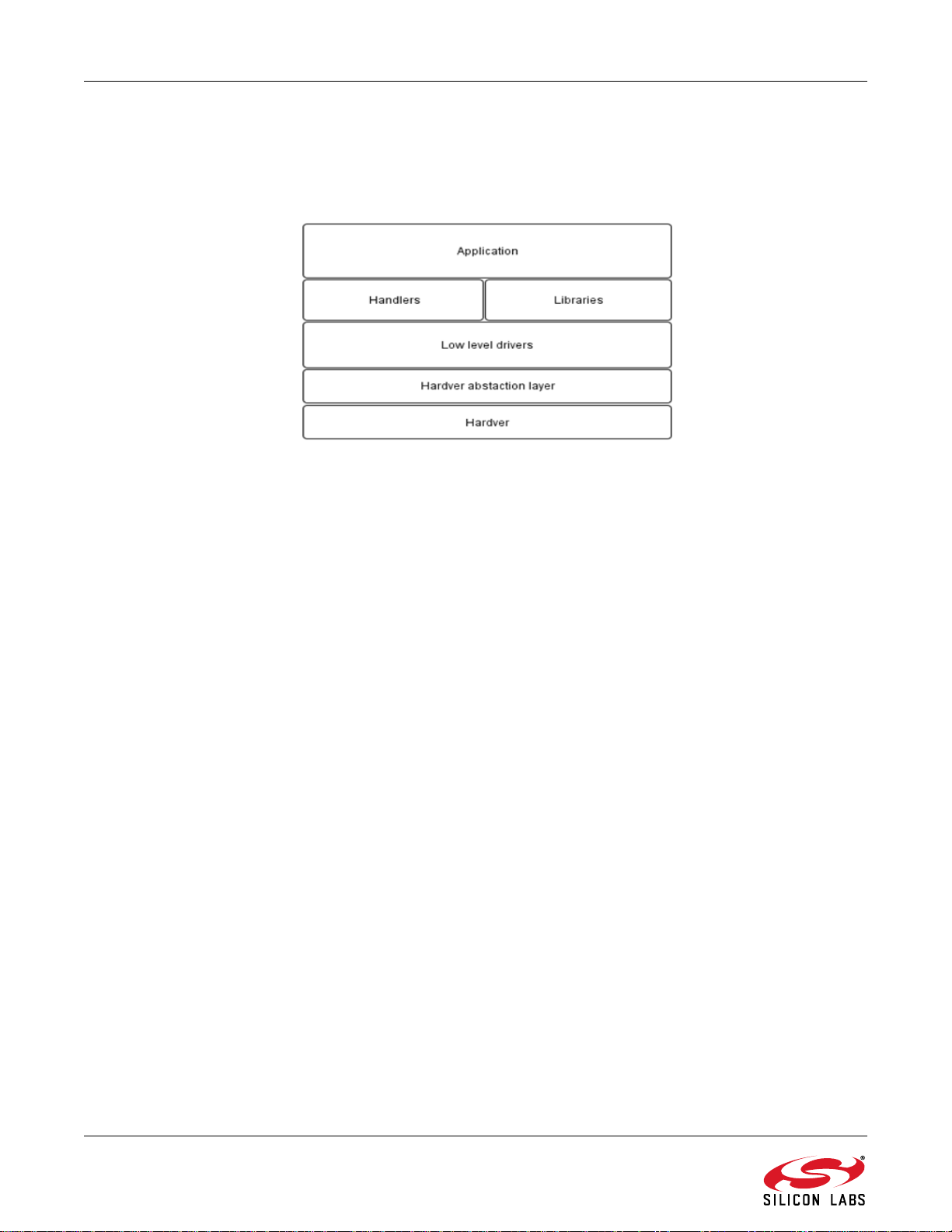
In all of the sample projects, the layered software approach is followed. There is a distinct scope for each software
module, and all modules can communicate through each other's API functions. The software modules are
separated and focused to cover one specific task. Figure 24 shows the software layers and its relations.
Figure 24. Software Layers of the Example Codes
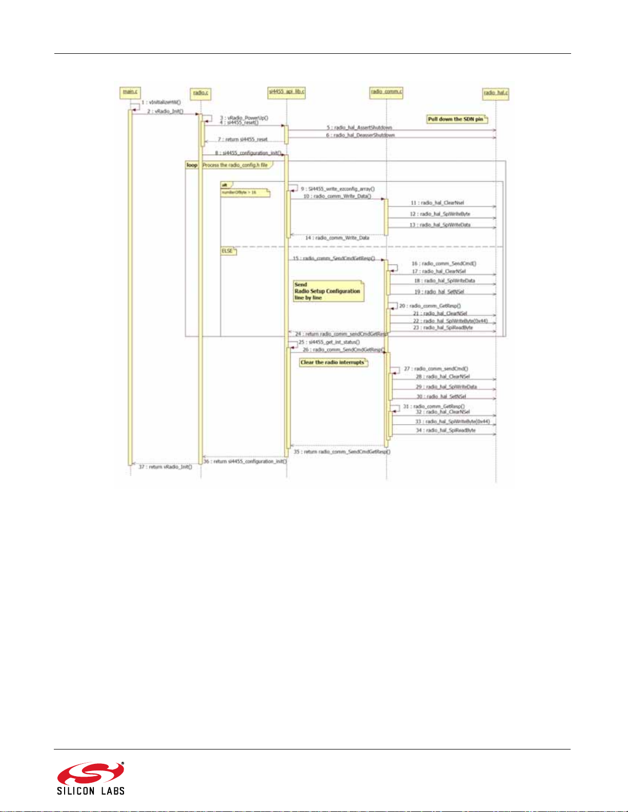
5.1.4. Radio Initialization in the Software Layers Perspective
Using the software layer approach, the example project can be understood easily. Each and every layer has its
own responsibility. If the upper layer, e.g. the "Application", wants to configure the hardware platform including the
host microcontroller and also the radio chip, it simply calls the hardware initial routine. The radio chip initialization is
started with a power on reset. The radio module sends a request to the si446x radio driver to reset the chip.
Thereafter, the driver forwards the request to the hardware abstraction layer that pulls down the SDN pin to
perform the power on reset. After the POR, the host MCU needs to send all the API properties to the radio via SPI
interface that means the "radio setup configuration" of the radio_config.h header file needs to be processed line by
line. The whole process of sending one API property and checking whether the radio is ready to receive the next
property is a repetitive task and is represented by a configuration loop. Finally, host MCU clears all the pending
interrupts of the radio.
28 Rev 0.4
Page 29
AN692
Figure 25. Function Calls During the Radio Initialization
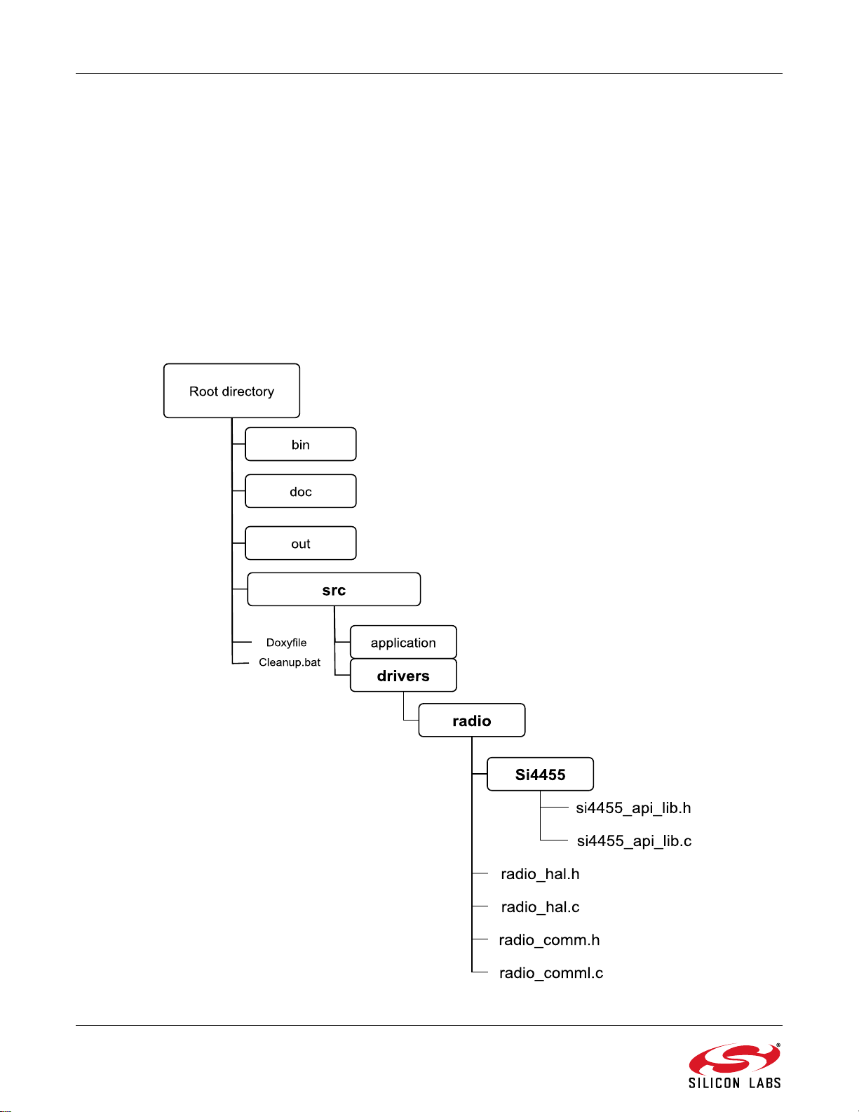
5.1.5. Directory Structure of the Example Project
All sample source code has a common directory structure with separated source and project files to ease the
understanding of the individual modules. For every sample project, the following directories and files can be found
in the main directory:
bin—Contains the SiLabs project files for Keil and SDCC compilers and the Makefile if the make tool is
used instead.
doc—Doxygen-generated documentation based on comments inside the source files in html format.
out—The outputs of the compilation process are sent to this folder. After successful compilation, this
directory contains files such as the hex file, the linker output, and the OMF file.
src—Directories containing the source files.
1. application
2. drivers
Doxyfile—This file contains the Doxygen documentation generator settings.
Cleanup.bat—Batch file used to delete all files generated during build process
Rev 0.4 29
Page 30
AN692
5.2. Example Projects Description
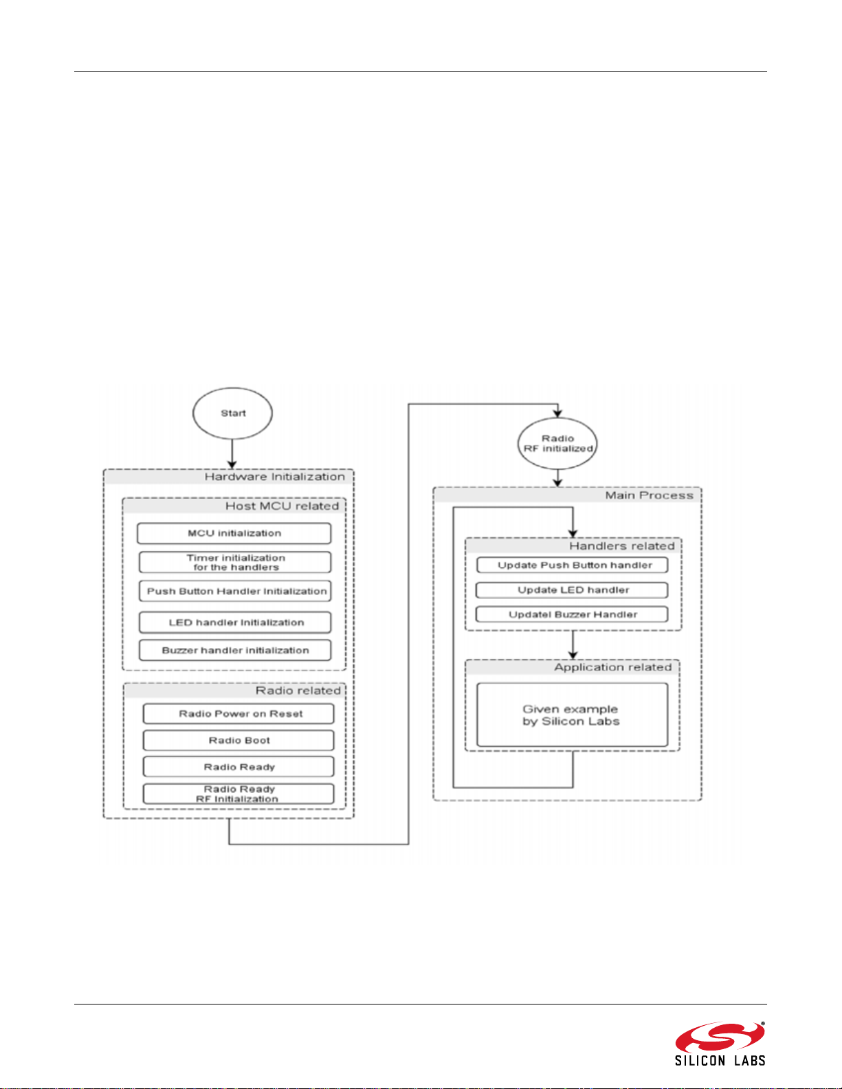
The general structure of an example project is shown in Figure 26. All the tasks are separated into two groups: the
"Hardware Initialization" part and the "Main Process" part. The Host MCU related tasks initialize the physical
interface between the radio and the controller unit, including the SPI lines (SCLK, SDI, SDO, NSEL) and general
I/O ports (SDN, NIRQ). After the interface has been initialized, the internal timer module is initialized to provide
precise timing for the handlers. Some example projects, such as the un-modulated carrier or the pseudo random
transmission projects, don't use handlers due to their simplicity. Handlers are for monitoring and changing the state
of the WMB peripherals. It is necessary to initialize the required handlers before using them. The radio related
tasks prepare the radio for the communication. The shutdown state may be entered by driving the SDN pin high.
When coming out of the shutdown state, a power on reset will be initiated along with the internal calibrations. After
the "POR" and the "BOOT" process, it is necessary to initialize the radio with the RF settings. It is highly
recommended to use the configuration header file (radio_config.h) generated by the Wireless Development Suite.
Manual editing in the header file can cause discrepancies and prevent the radio from working correctly. After the
radio is initialized, the Main Process has to continuously update the peripheral handlers and process the user
application code. The radio can be controlled from a high level due to the layered, customizable, user friendly radio
driver module.
Figure 26. General Structure of an Example Project
The example codes can be exported from the Wireless Development Suite software. Since the "radio_config.h"
configuration header file is highly customizable by the WDS software tool, there are no dedicated default
parameters for the example projects.
30 Rev 0.4
Page 31
AN692
5.2.1. Continuous Wave (CW) and Pseudo Random (PN9) Transmission
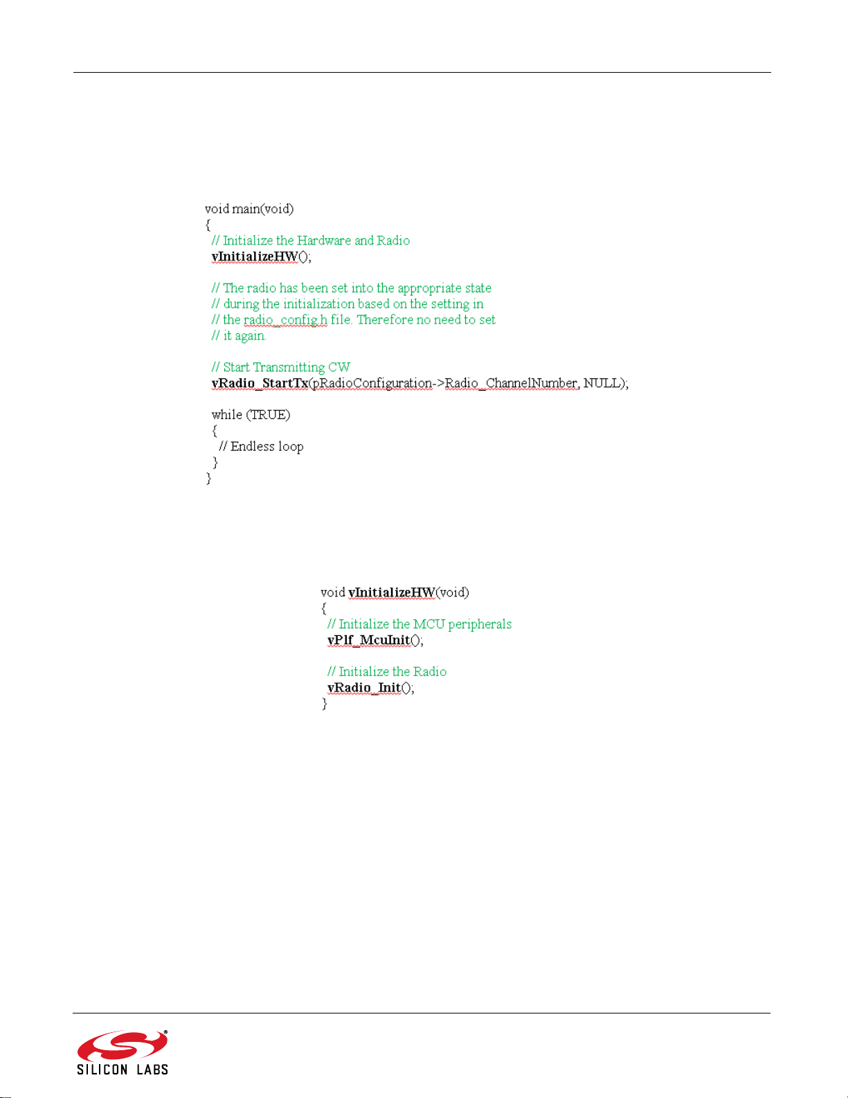
This example project demonstrates the EZConfig method for setting up the radio chip. In the main() function, there
is only a function call to the vInitializeHW(). After the hardware and radio initialization, CW transmission starts.
Since the MCU has no more tasks once the radio has been initialized, an empty infinite loop keeps running while in
the cycle.
The vInitializeHW() invokes initialize functions for the MCU IOs and peripherals and for the radio chip itself. The
vPlf_Mcuinit() should be called before the vRadio_Init() function because the radio initializer assumes that the
radio related IOs are already configured as well as the SPI peripheral in order to communicate with the radio chip.
The vRadio_Init() function, already discussed in the Radio Configuration chapter, is responsible for loading the
EZConfig array and setting the radio registers according to the configuration specified in radio_config.h. Depending
on which radio configuration was compiled into, the same project can set the radio to produce Carrier Wave, to
transmit Pseudo Random (PN9) sequence with the specified modulation on the desired frequency, or even to
handle direct mode transmission and reception. The above mentioned operating modes of the radio requires no
intervention from the MCU except the configuration process, therefore, the same project can be used for all of
them. The only modification needed to change the radio operating mode is to replace the radio_config.h file with
the one generated by the Wireless Development Suite for the required operation.
Rev 0.4 31
Page 32
AN692
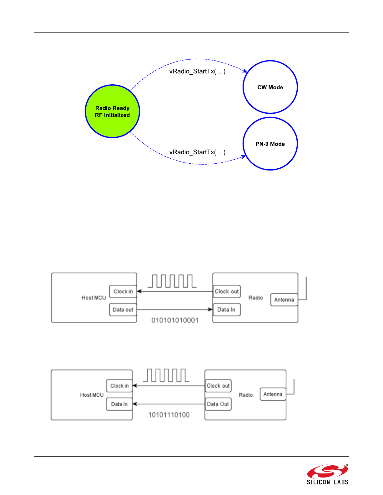
Figure 27. Activate CW/ PN9 Mode
5.2.2. Direct Mode Transmission and Reception
The source code for this operating mode is the same as the one used for Continuous Wave or PN9, except the
radio configuration properties have been changed to direct mode RX/TX.
The radio in direct mode can be used if an external MCU is connected to its RX/TX GPIOs in order to receive or
transmit arbitrary data. The radio interrupt sources in this mode can still be used; for example, the Preamble Detect
or Sync Word Detect interrupt will work in this mode too.
The direct mode is useful when already existing proprietary communication protocol has to be implemented using
Silicon Laboratories radio transceivers.
Figure 28. GPIO Connections between the Radio and the Host MCU (Direct TX)
Figure 29. GPIO Connections between the Radio and the Host MCU (Direct RX)
32 Rev 0.4
Page 33
AN692
5.2.2.1. Direct Mode RX
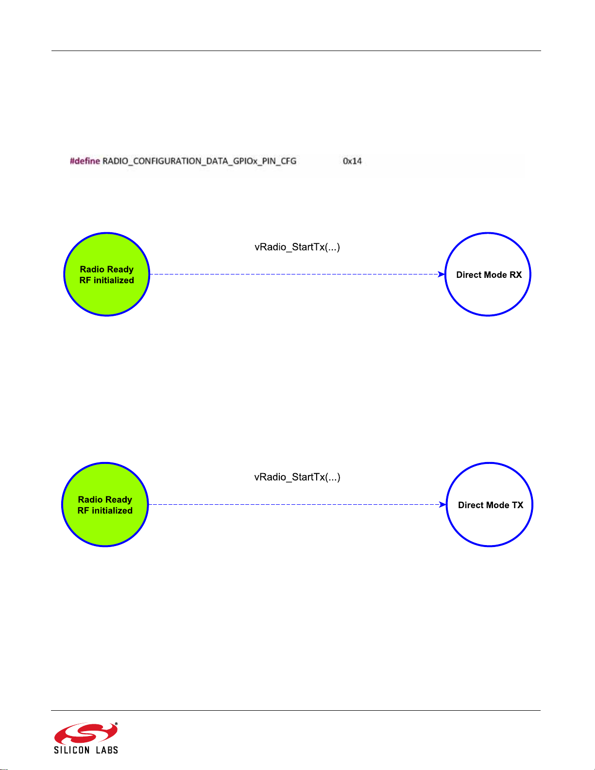
In RX direct mode, the RX Data and RX Clock can be programmed for direct (real-time) output to GPIO pins. The
microcontroller may then process the RX data without using the FIFO or packet handler functions of the RFIC.
The GPIOs of the radio used for the RX_DATA and RX_DATA_CLK output can be changed without generating a
new configuration file again. In the radio_config.h file, insert or modify the definition for the given GPIO as shown
below.
Replace the value with the corresponding property value. For the GPIO configuration options and values, refer to
the API documentation.
Figure 30. Activate Direct RX Mode
5.2.2.2. Direct Mode TX
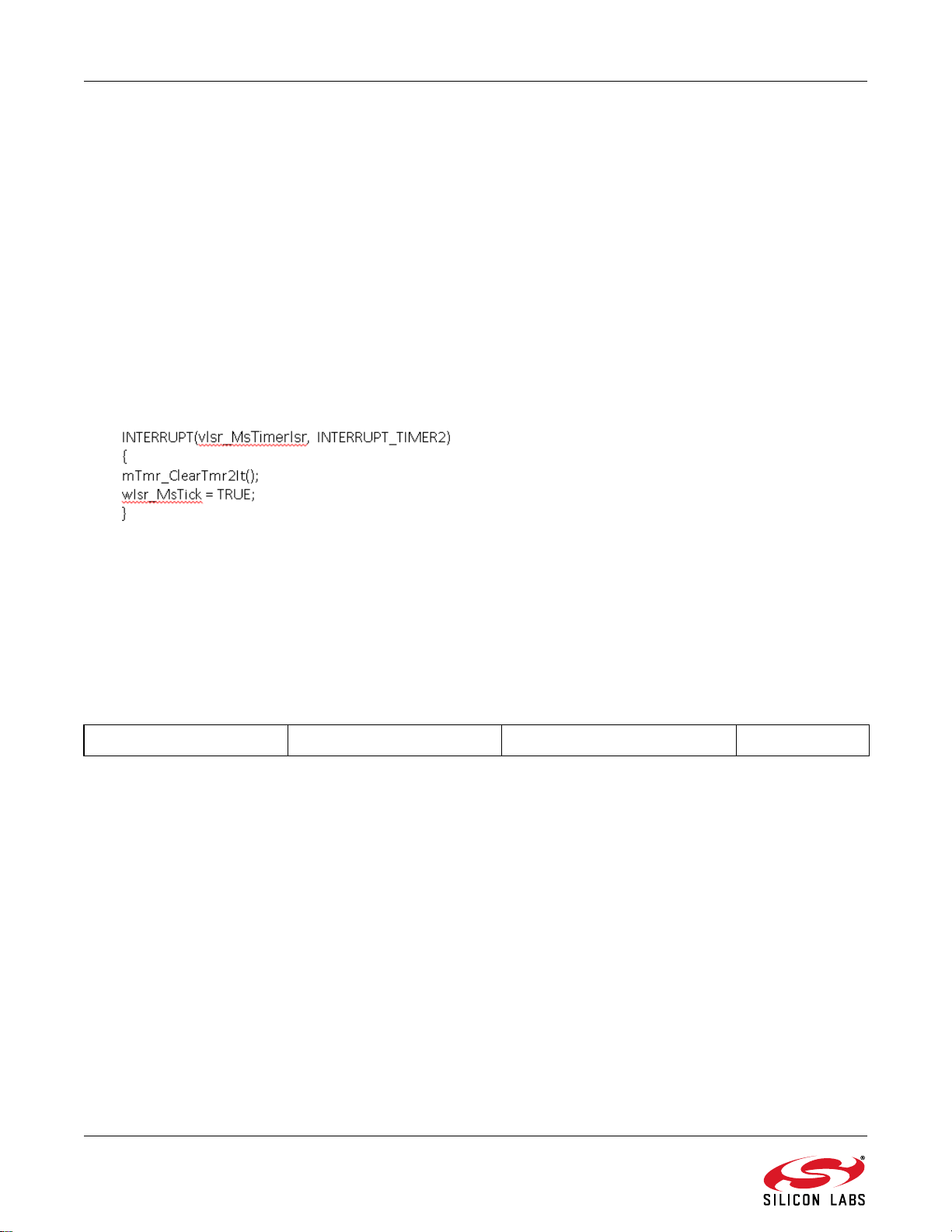
The radio can be used in direct transmission mode. In this mode the data to be sent should be fed externally to the
radio chip using one of its GPIOs. The GPIO used to input TX_DATA is configured by the EZConfig array, which
means that a new EZConfig array will be generated each time this pin is changed. Optionally, the TX_DATA_CLK
output can be changed via replacing the desired GPIO define value with the corresponding TX_DATA_CLK value.
This modification doesn’t require new EZConfig Array generation. For the GPIO configuration options and values,
refer to the API documentation.
Figure 31. Activate Direct TX Mode
Rev 0.4 33
Page 34
AN692
5.2.3. Transmission of a Simple Packet in Packet Handler Mode
This example project demonstrates the usage of the radio chip in fixed packet length mode and utilizes the
advantages of the Packet Handler feature.
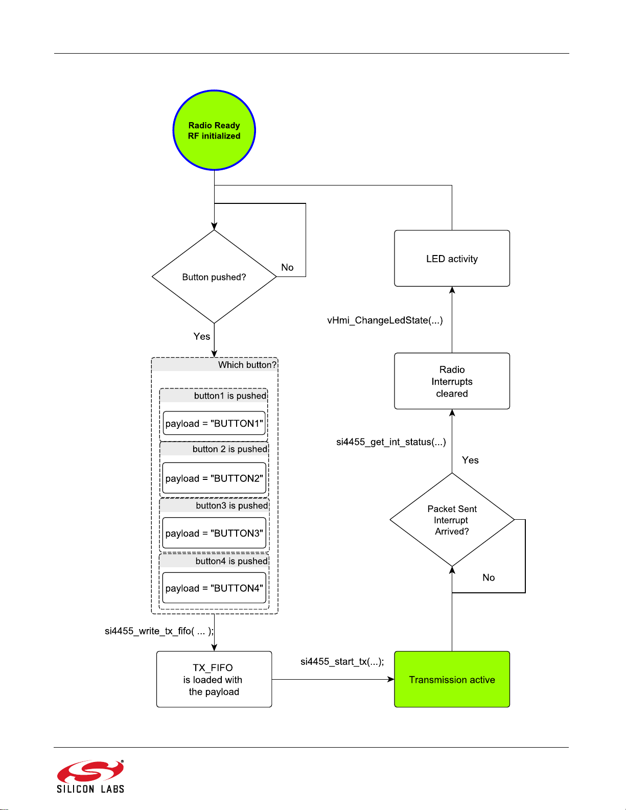
This example project uses the radio to transmit the “BUTTONx” packets, where “x” value can be “1–4” depending
on which button was pressed. Once the packet is sent to the radio, it blinks the corresponding LED on the board.
The transmitter part of this example project configures the radio parameters such as frequency, data rate, and
modulation using the EZConfig Array generated by WDS. It also sets the Packet Handler properties to use fixed
packet length with CRC check.
These custom properties enable the Packet Handler interrupts and the packet sent interrupt source.
The application code uses the Human Machine Interface software module in order to handle the push button
events and blink LEDs. Both handler functions are scheduled to run once in every 1 ms.
The Demo_App_Pollhandler() function is outside of the scheduled tasks to guarantee the fast response if a radio
interrupt occurs. These timing intervals are generated by the Timer2 peripheral overflow interrupt. The Interrupt
Service Routine (ISR) for this interrupt can be found in isr.c source file.
The DemoApp_Pollhandler() function continuously checks if the packet has been sent by checking the Packet
Handler interrupt of the radio. When a packet is successfully sent, the function blinks the LED corresponding to the
pressed button.
In order to limit the packet resending frequency, there is a PACKET_SEND_INTERVAL macro defined. After a
packet starts to transmit, the next packet transmission can be started only after the defined time interval elapsed.
The return value of the vSampleCode_SendFixPacket() function is TRUE when a button pressed event has
occurred. This also means that a packet has been written to the radio FIFO and is waiting for transmission. The
used packet structure is shown in the following table:
Preamble Sync Word Payload CRC
32–40 bits 2 byte 7 byte byte
34 Rev 0.4
Page 35
AN692
Figure 32. Transmission Flowchart
Rev 0.4 35
Page 36
AN692
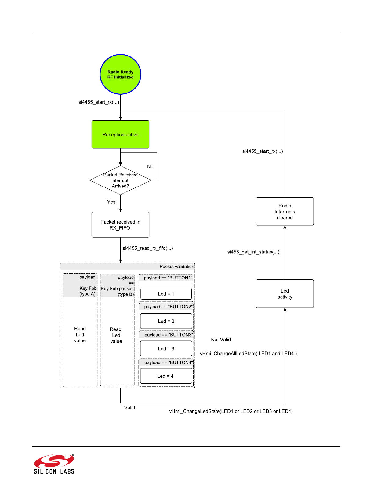
5.2.4. Reception of a Simple Packet in Packet Handler Mode
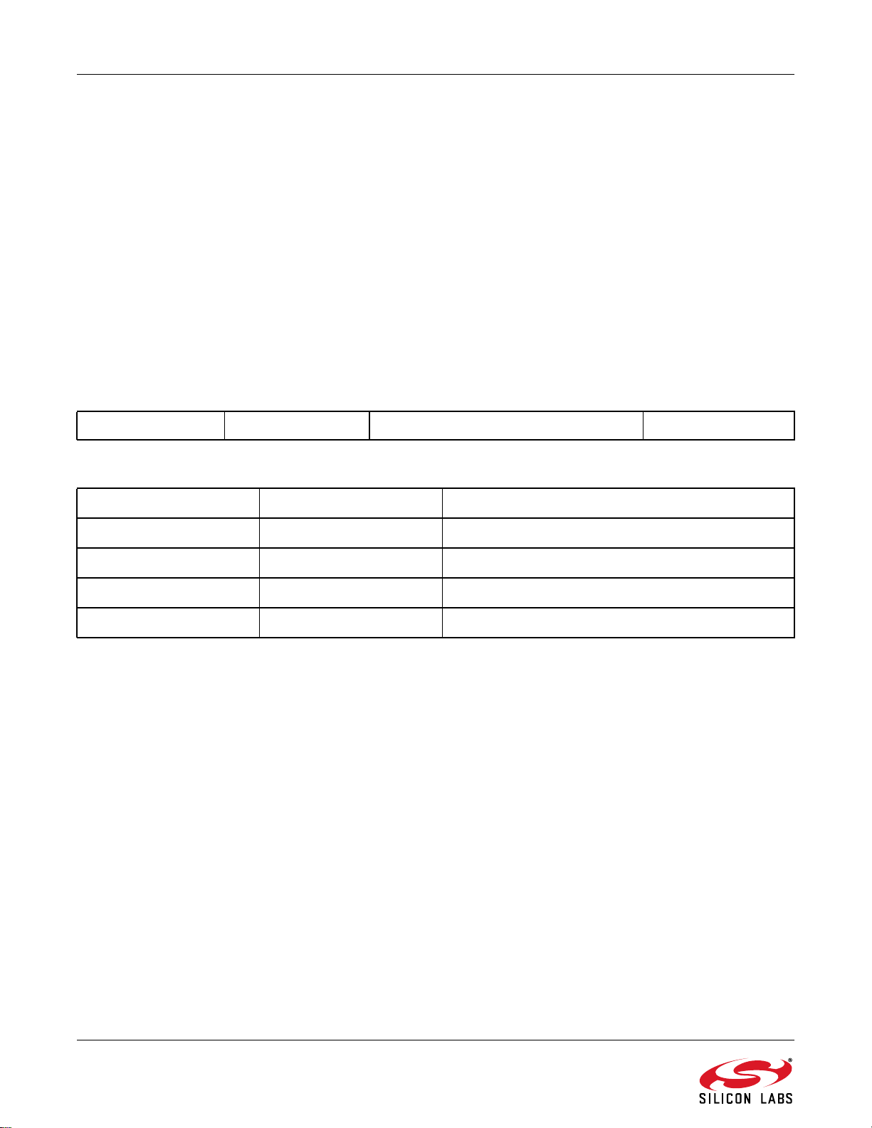
This example project demonstrates the usage of the radio chip for reception in fixed packet length mode and
utilizes the advantages of the Packet Handler feature. This project uses the Human Machine Interface software
module that is used in the transmitter side project as well. The handler functions for the push buttons, LEDs, and
buzzer are also scheduled on a 1 ms time base.
The DemoApp_Pollhandler() function also runs outside the scheduled tasks in order to provide fast response if a
radio interrupt occurs. The difference between the transmitter and receiver project scheduled tasks is that the
receiver project uses the Buzzer handler function. This is required as the receiver side beeps when a valid packet
is received. The packet validity has been already verified by the Packet Handler as the CRC calculation is enabled
on the packet payload. The radio interrupt occurs only when a packet with valid CRC is received. The radio won’t
generate interrupt on a packet with a CRC error because this interrupt source is disabled. According to the StartRX
condition in vRadio_StartRX() function, the chip remains in RX state in these cases.
The DemoApp_Pollhandler() function checks if a valid packet has been received and if it contains the expected
information regarding which button was pressed on the transmitter side. If the information is correct, it blinks the
same LED. The payload has its pre-defined content, namely "BUTTONx" where x can be 1, 2, 3, or 4.
This packet is generally used in different example codes for EZRadio transceivers.
Preamble Sync Word Payload CRC
32-40 bits 2 byte 7+N byte byte
Number of Bytes Field Name Description
4-5 Preamble 0xAA
2 Sync 0x2D, 0xD4
7 Payload “BUTTONx”
2 CRC-16 Generator X16+X15+X2+1, start value 0xFFFF
36 Rev 0.4
Page 37
AN692
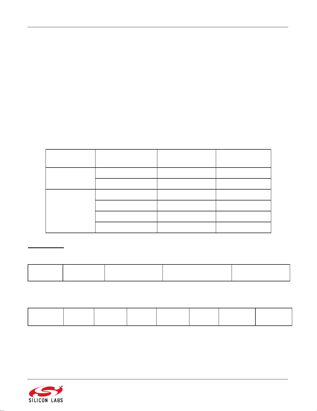
5.2.4.1. Key Fob Compatibility with the Si4x55 RF Receiver
This section is intended to describe the compatibility between the Si4x55 RF IC working as a receiver and different
key fobs working as transmitters. Silicon Labs provides two types of demo kits containing key fobs with different
packet structures.
1. Demo kits with the key fob packet type #1 (obsolete).
These kits contain a key fob transmitter with Si4010 that is preprogrammed with the "rke_demo" example
code. These keyfobs transmit packet type #1
a. Si4010 Key Fob Demo Kit with AES Capability XXXMHz (P/N: 4010-DAAKF_XXX)
b. Si4010 Simplified Key Fob Demo Kit XXXMHz (P/N: 4010-DASKF_XXX)
2. Demo and Development kits with the key fob packet type #2:
These kits contain a key fob transmitter with Si4010 that is preprogrammed with the "rke_demo_2"
example code. These keyfobs transmit packet type #2
a. Si4010 Remote Keyless Entry Demo Kit with AES Encryption (P/N: 4010-AESK1W-XXX)
b. EZRadio Remote Control Demo Kit XXXMHz (P/N: EZR-LEDK1W-XXX)
Table 7. Keyfob Used Frequencies
Project Name Modulation Type Center Frequency
[MHz]
FSK 433.39 60
“rke_demo”
FSK 868.96 50
FSK 316.66 43
FSK 433.92 59
“rke_demo_2”
FSK 868.30 119
FSK 917.00 120
Packet type #1 (obsolete)
The structure of the packet:
Preamble Sync Word Function Control Byte One’s complement of
4 byte 2 byte 1 byte 1 byte 1 byte
The structure of the Function Control Byte:
Function Byte
Deviation
[kHz]
Function Control Byte
OUT3
F1
OUT0–OUT3 represent the four LED outputs of the receiver. Output functions are controlled by the F0–F1 function
bits.
Function bits operations:
OUT3
F0
OUT2
F1
OUT2
F0
Rev 0.4 37
OUT1
F1
OUT1
F0
OUT0
F1
OUT0
F0
Page 38
AN692
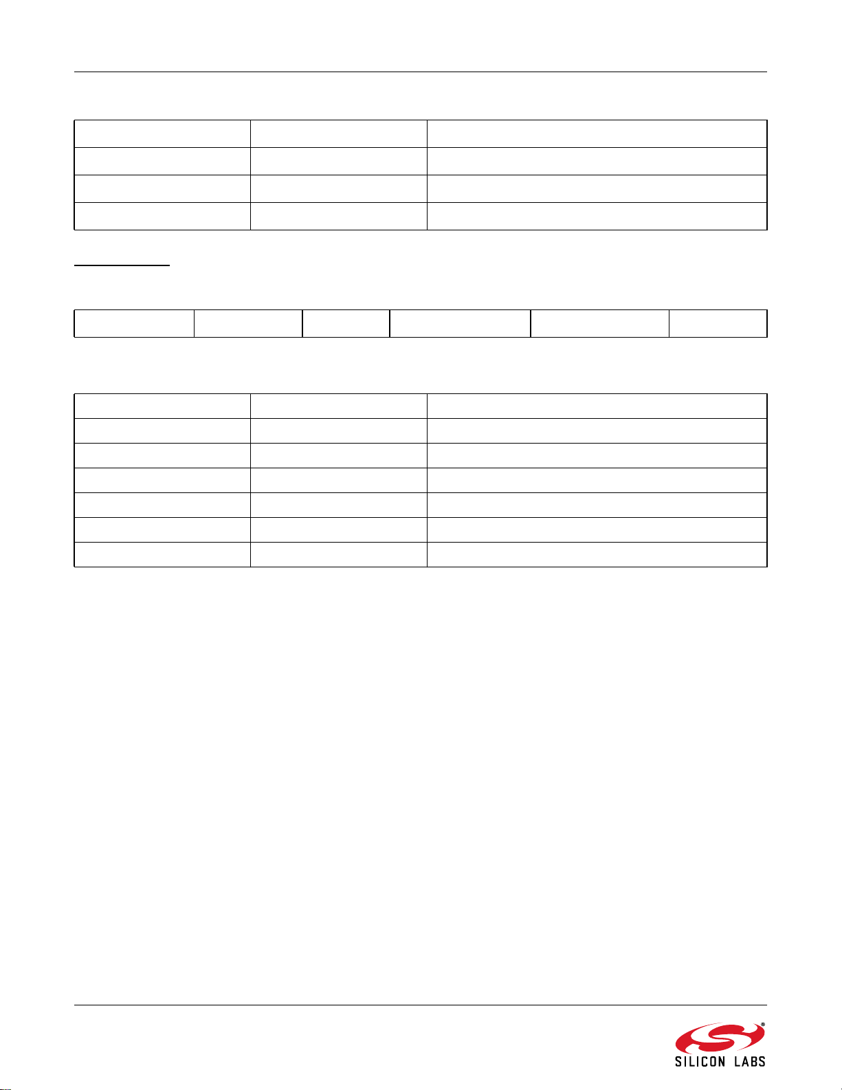
F1 F0 Function
0 0 No change
0 1 Sets output logical low (LED is OFF)
1 0 Sets output logical high (LED is ON)
Packet type #2
The structure of the packet:
Preamble Sync Word Chip Id Status Packet Count Crc
13 byte 2 byte 4 byte 1 byte 2 byte 2 byte
Number of Bytes Field Name Description
13 Preamble 0xAA
2 Sync 0x2D, 0xD4
4 Chip Id Unique, factory-burned chip ID
1 Status Lower 5 bits are the button information
2 Packet Count Rolling counter
2 CRC-16 Generator X16+X15+X2+1, start value 0xFFFF
38 Rev 0.4
Page 39
AN692
Figure 33. Reception Flowchart
Rev 0.4 39
Page 40

AN692
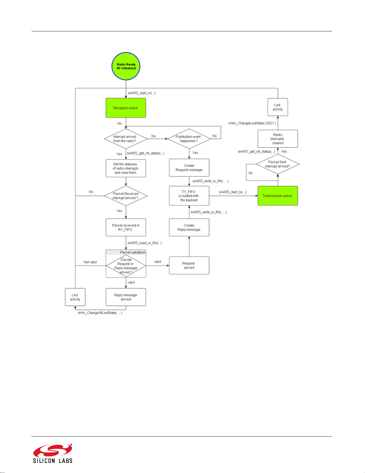
5.2.5. Bidirectional Variable Length Packet Based Communication
This example project uses the radio both in receive and transmit mode in order to establish a two-way link between
two demo boards. At startup, the radio is initialized according to the settings in radio_config.h file. The Packet
Handler in the radio is configured to receive variable length packets from the transmitter. The following table shows
the packet structure used in this example project.
Preamble Sync Word Length Payload CRC
32–40 bit 16 bit 8 bit N bit 16 bit
The LENGTH field contains the information on how many byte the PAYLOAD size is. Following the PAYLOAD field,
there is a CRC field calculated over the LENGTH and PAYLOAD field to ensure error-free packet reception. The
radio is configured to produce interrupt signal the packet is successfully received or transmitted. This is done by
custom interrupt property setting in radio_config.h
Once the radio and the MCU peripherals and IOs are initialized, a start RX command is issued to the radio.
The Human Machine Interface handler functions are scheduled in the 1 ms tasks.
The radio is in continuous RX state until a packet has been received or a button pressed event occurs.
If a button is pressed, a specific message is loaded to the radio’s TX FIFO and the radio changes its state to TX.
Depending on which button has been pressed, the PAYLOAD length will vary. After the transmission has been
done, the radio switches back to RX state and waits for acknowledge message from the other board. A certain LED
on the board blinks according to the pressed button.
When a packet is received while the radio is in RX state, the PAYLOAD field will be analyzed. If it contains a valid
message, the board sends back an acknowledge message and blinks its appropriate LED according to the button
pressed. If an acknowledge message was received by the transmitter node, it beeps its buzzer and blinks all LEDs
on the board. The bRadio_Check_TX_RX() function is used to check the radio interrupt status and read which
interrupt occurred.
The DemoApp_Pollhandler() is located outside the scheduled tasks in order to be able to respond quickly to the
radio interrupts. It checks if the radio has any pending interrupt.
A state machine has been implemented to handle the interrupts.
The type of the message received is determined from the LENGTH field information. When sending a variable
length packet, the length of the PAYLOAD must be written to the TX FIFO first, then the message to be sent. When
a packet received interrupt is pending, the bRadio_Check_TX_RX() function has already loaded the message
content in the variableRadioPacket array.
The validity of the packet has already been verified by the Packet Handler as the CRC verification enabled so it
guarantees the payload is error-free.
40 Rev 0.4
Page 41
AN692
Figure 34. Bidirectional Variable Packet Example Project Flowchart
Rev 0.4 41
Page 42
AN692
5.2.6. Continuous Transmission of Custom Amount of Standard Packets
The purpose of the standard packet transmission example code is to demonstrate how the radio can send packets
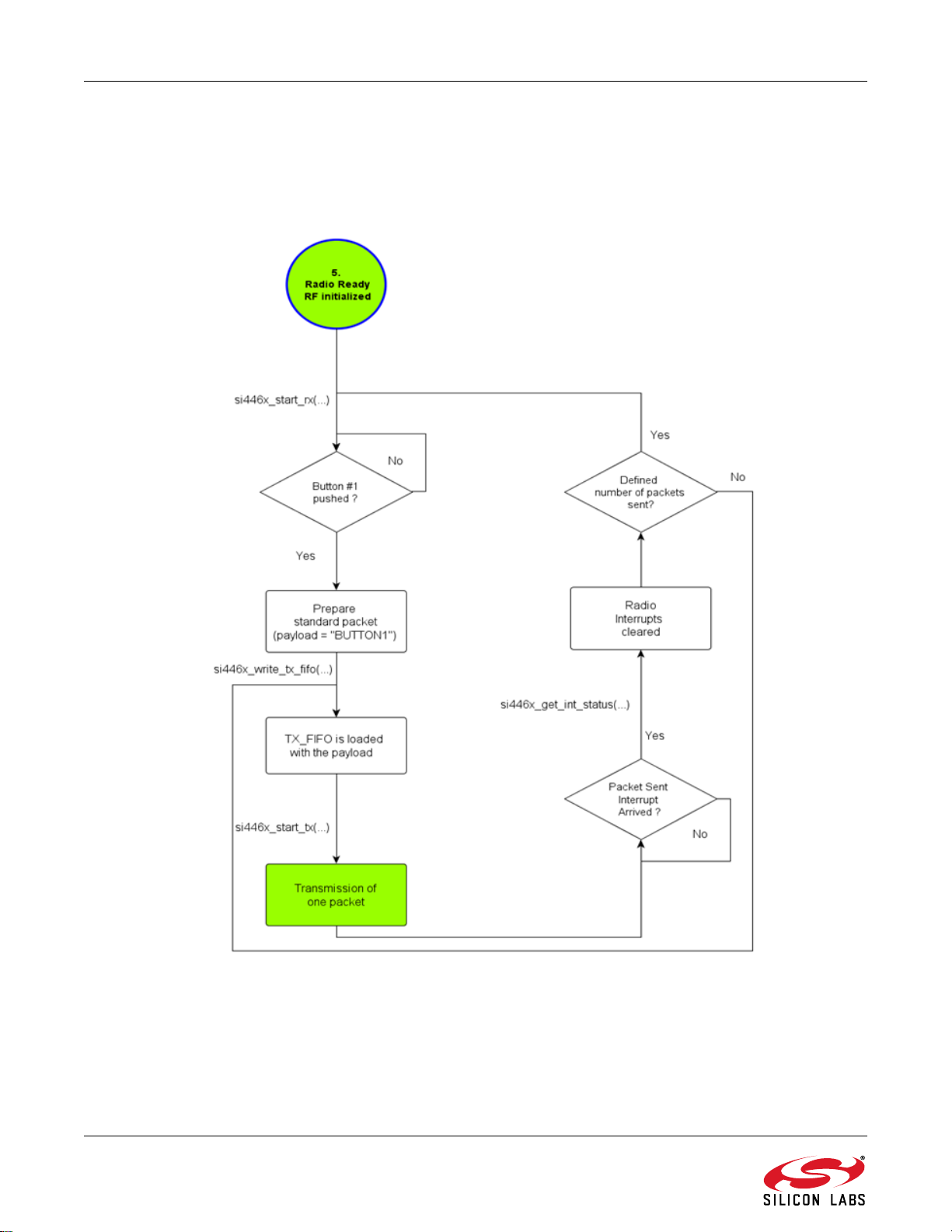
in FIFO mode continuously. If the first button is pressed on the Wireless Motherboard then the host MCU will load
the pre-defined content, namely “BUTTON1” in TX_FIFO and after that will send it. Pressing the button once
prompts the radio to send the specified number of the same packets sequentially.
Figure 35. Continuous Transmission Flowchart
This project is the transmitter side of the low duty cycle receiver project. It can send a custom amount of packets in
order to satisfy the needs of the receiver side namely to determine the minimum number of packets to be
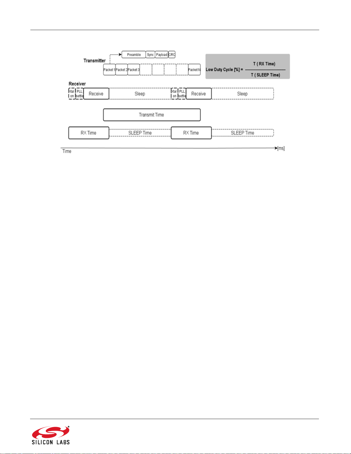
transmitted so that the receiver working in low duty cycle mode can certainly receive the packet. In the LDC mode
the radio sleeps a certain amount of time called “Sleep time” then wakes up and listens for the signal in the “RX
time”.
42 Rev 0.4
Page 43
AN692
Figure 36. General Usage of the Continuous Transmission
In order to calculate the minimum number of packets to be transmitted, it is necessary to know how the different
time periods, such as the “Transmit Time”, the “RX Time” and “Sleep Time” relate to one another in the worst case
scenario. If the transmitter starts to transmit just after the receiver entered sleep mode, the transmitter needs to
transmit while the receiver is in sleep mode plus the receiver wakes up and still a packet needs to be transmitted.
mi n Tr an s mi t TimeT SL E EP TimeT X Ta l on PL L settle+T on e packet++=
Rev 0.4 43
Page 44
AN692
5.2.7. Host MCU Implemented Low Duty Cycle
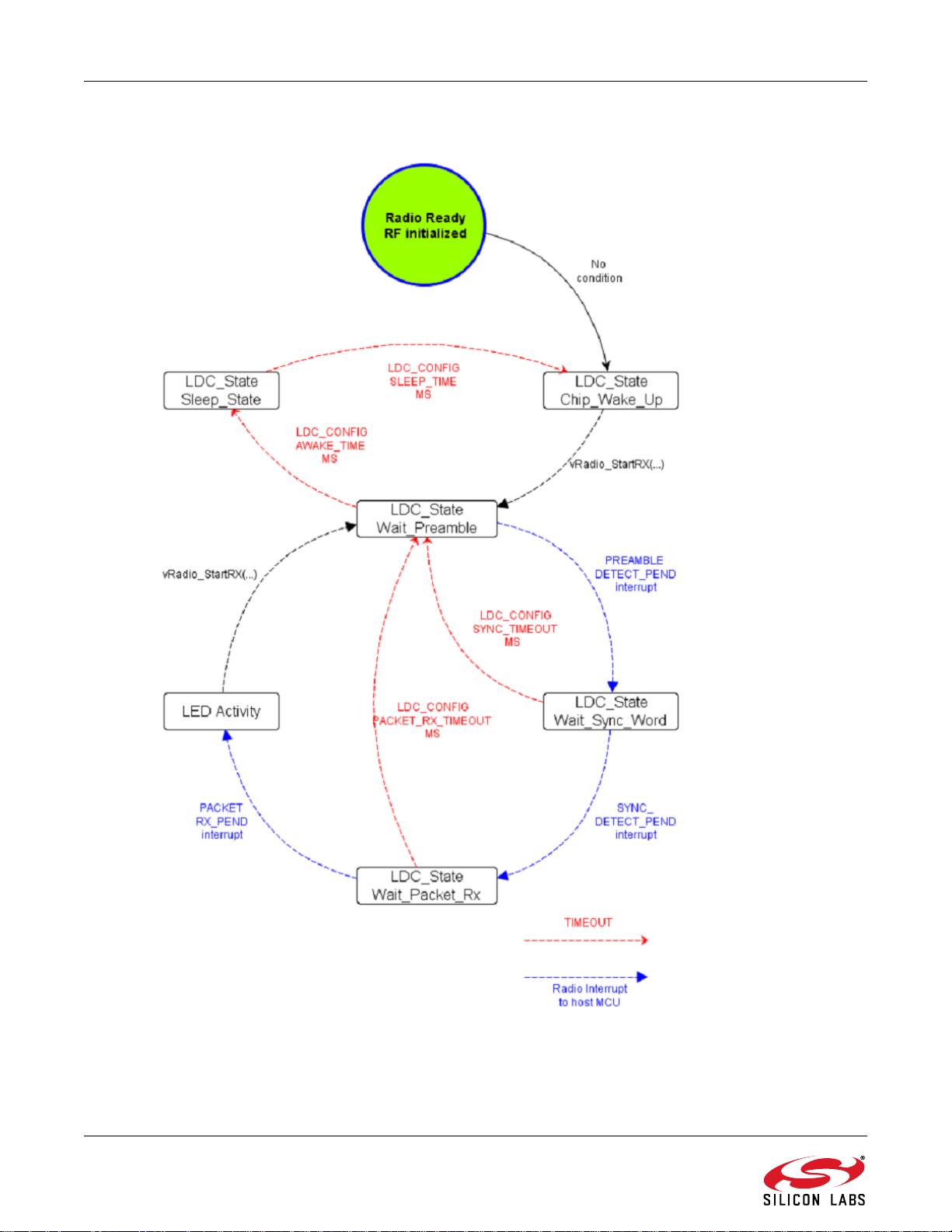
Figure 37. Host MCU Implemented Low Duty Cycle Flowchart
44 Rev 0.4
Page 45
AN692
The basic operation of low duty cycle mode is shown in Figure 37. The host MCU periodically wakes up the radio
chip to work in reception mode. If a valid preamble is not detected within the "LDC_CONFIG_AWAKE_TIME_MS"
time, the host MCU forces the receiver to "LDC_State_Sleep State" state and it remains in that mode until the
"LDC_CONFIG_SLEEP_TIME_MS" time elapses. If a valid preamble is detected, signed by
"PREAMBLE_DETECT_PEND" interrupt, the receiver gets into "LDC_State_Wait_Sync_Word" state. If a valid
sync word is not detected within the "LDC_CONFIG_SYNC_TIMEOUT_MS" time, the host MCU forces the
receiver to "LDC_State_Wait_Preamble" state. If a valid sync word is detected and signed by
"SYNC_DETECT_PEND" interrupt, the receiver gets into "LDC_State_Wait_Packet_Rx" state. If the whole packet
is not received within "LDC_CONFIG_PACKET_RX_TIMEOUT_MS" time, the host MCU forces the receiver to
"LDC_State_Wait_Preamble" state. If the packet is received successfully and signed by "PACKET_RX_PEND"
interrupt, the host MCU reads the RX FIFO's content and flashes the appropriate LED(s). After finishing the LED
activity, host MCU starts the reception by vRadio_StartRX( )function. The example code is capable of receiving
three types of packets previously described in the "Reception of a Simple Packet in Packet Handler Mode". The
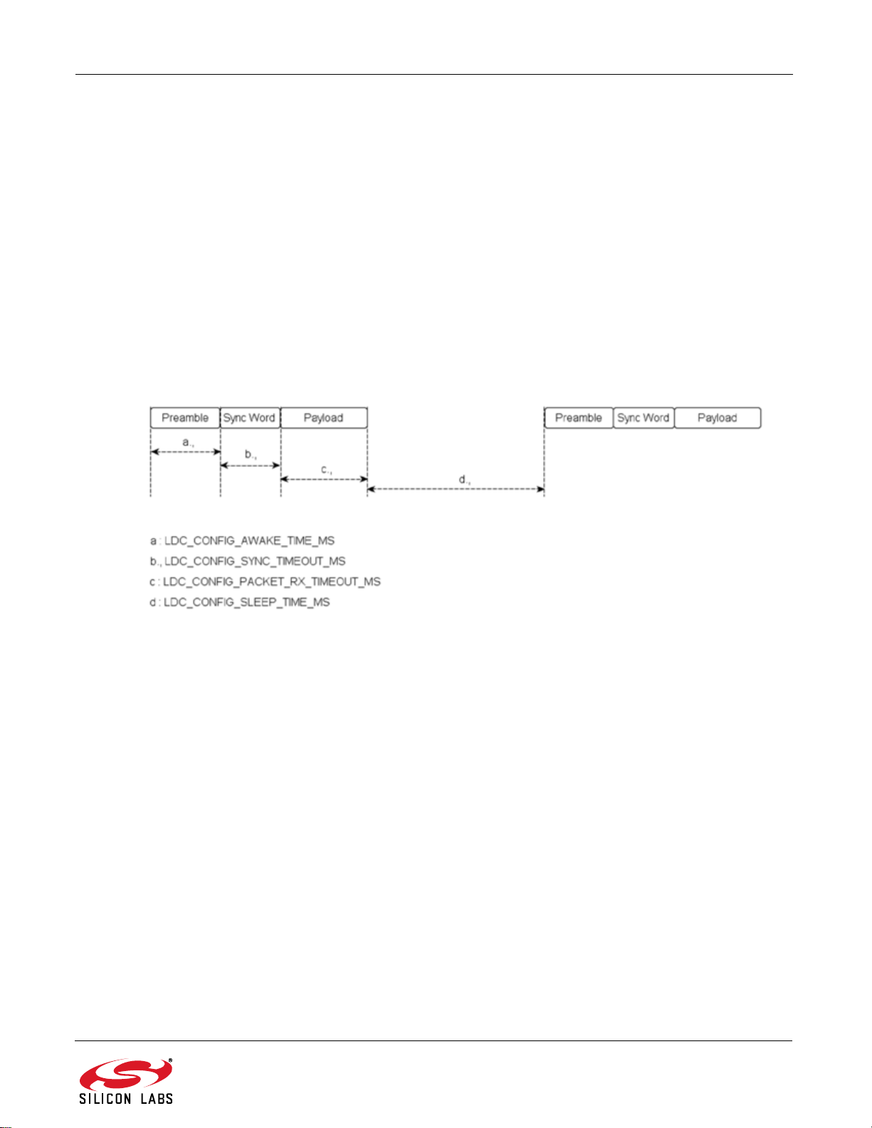
timeout periods can be configured in the "ldc_config.h" header file in ms unit. Note that the low duty cycle feature is
not implemented internally in the radio chip, but the host MCU controls the internal state of the radio.
Figure 38. Configurable Packet Related Time Intervals in the Host MCU
Rev 0.4 45
Page 46
AN692
5.2.8. Long Packet Transmission
Applications requiring transmission of packets longer than the TX FIFO size (64 bytes) may use the long packet
feature of the radio. In this case, TX FIFO Almost Empty Interrupt should be monitored for proper timing to fill the
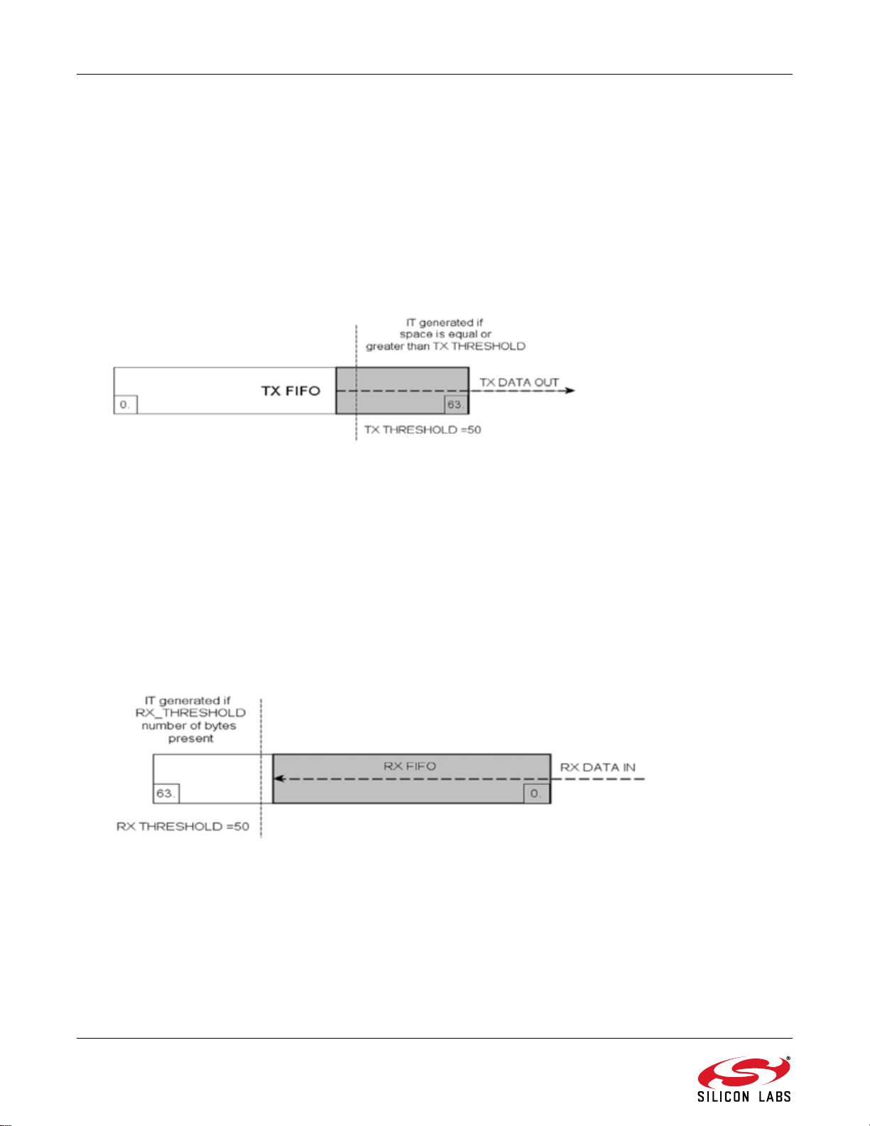
TX FIFO. To control when the Almost Empty Interrupt should actually occur, a threshold level can be set. For the
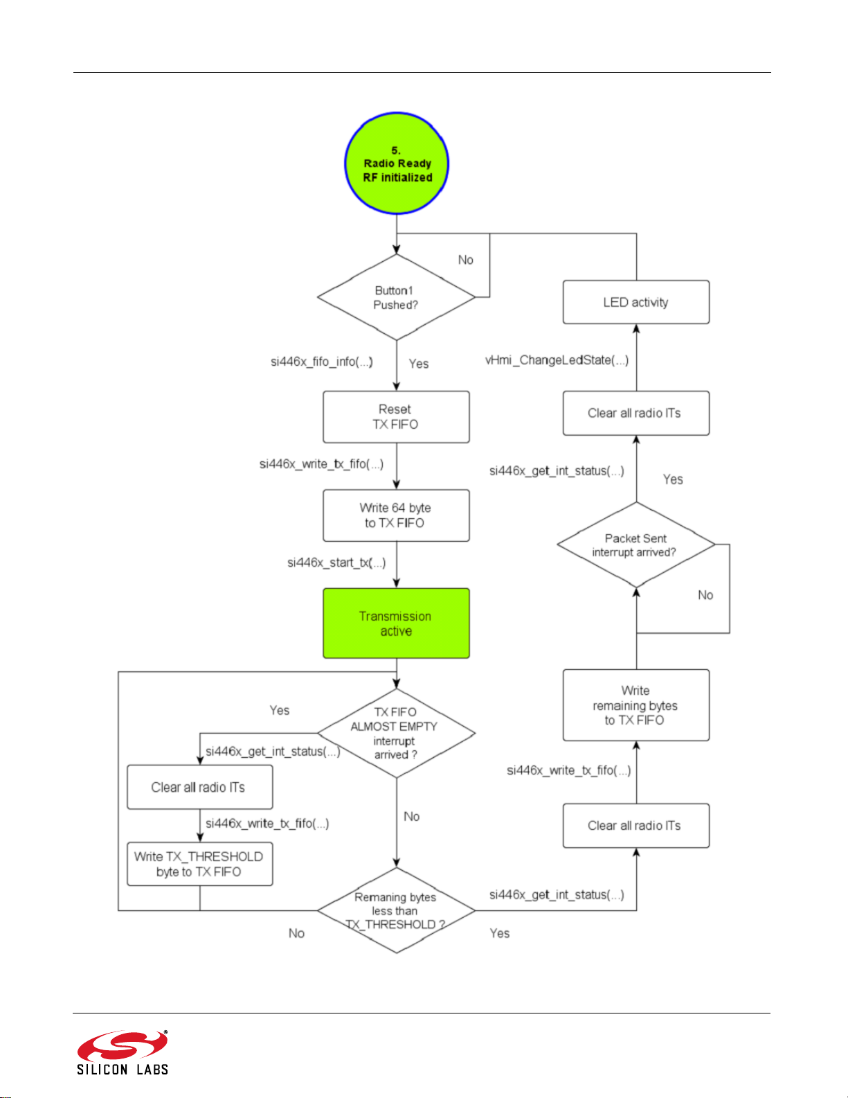
TX side of the link, the TX FIFO Almost Empty and Packet Sent interrupts have to be enabled during initialization.
Upon a button push, the first 64 bytes are filled into the TX FIFO and the host MCU starts waiting for a TX FIFO
Almost Empty interrupt. When the interrupt arrives, the host MCU fills TX_THRESHOLD number of bytes into the
FIFO, and then goes back to the state in which it is waiting for the next TX FIFO Almost Empty IT, and so on. If
there are fewer bytes left to transmit than the TX_THRESHOLD, they are put into the FIFO and the host MCU waits
for the packet sent interrupts.
Figure 39. Occurrence of TX FIFO Almost Empty Interrupt
5.2.9. Long Packet Reception
Applications requiring reception of packets longer than the RX FIFO size (64 bytes) may use the long packet
feature of the radio. In this case, RX FIFO Almost Full Interrupt should be monitored for proper timing to read the
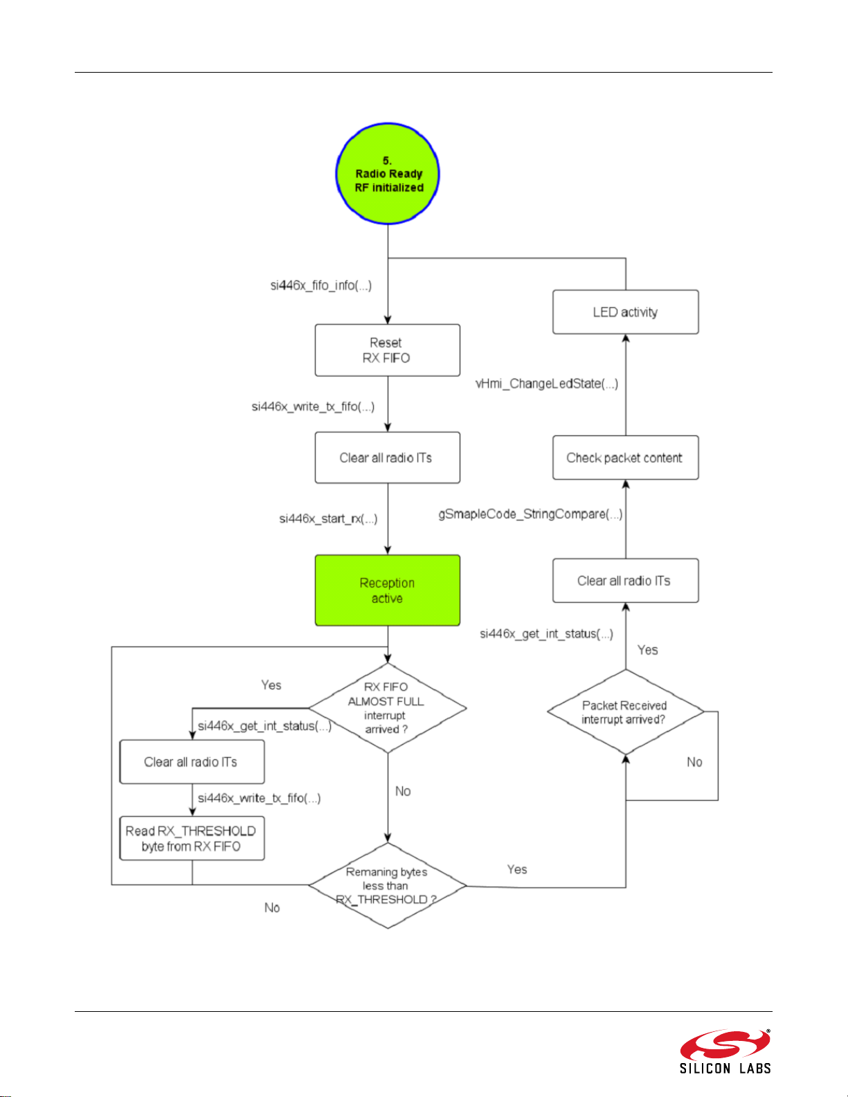
RX FIFO. To control when the Almost Full Interrupt should actually occur, a threshold level can be set. For the RX
side of the link, the RX FIFO Almost Full and Packet Sent interrupts have to be enabled during initialization. After
sending a START_RX command, the host MCU begins waiting for the RX FIFO Almost Full IT. When it arrives, it
reads out RX_THRESHOLD number of bytes from the RX FIFO and continues waiting for the next RX FIFO Almost
Full Interrupt, etc. If there are fewer bytes left to receive than RX_THRESOLD, the host MCU should wait for the
packet received interrupt.
Figure 40. Occurrence of the RX FIFO Almost Full Interrupt
46 Rev 0.4
Page 47
AN692
Figure 41. Long Packet Transmission Flowchart
Rev 0.4 47
Page 48
AN692
Figure 42. Long Packet RX Flowchart
48 Rev 0.4
Page 49
AN692
5.2.10. Empty Project
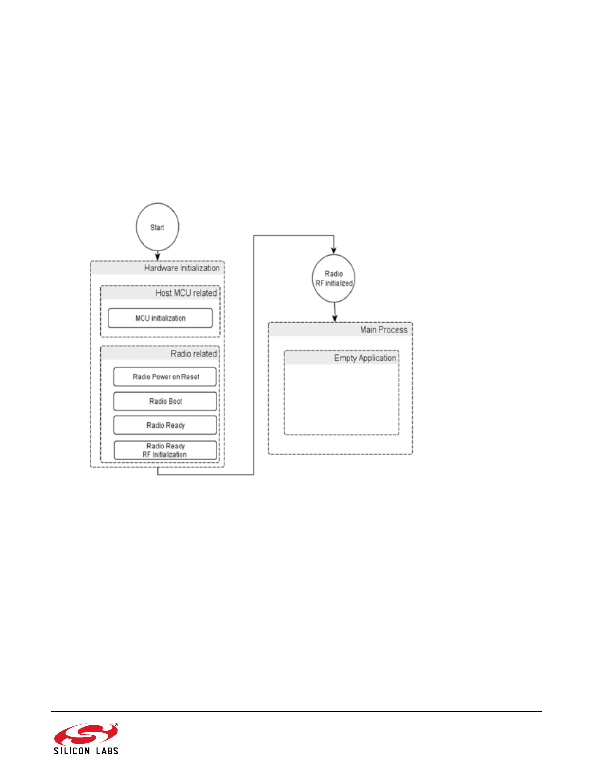
The empty project is created to help users start writing their custom firmware. The project follows the convention
for directory structure introduced in the example projects. It contains driver modules for the radio and MCU
peripherals as well as a default MCU initialization procedure. The porting of an example project to an MCU of
choice can be done easily thanks to the layered approach of the project structure. This approach reduces the effort
required to compile the code for other architecture, as only the low-level functions must be modified. The general
structure of the project can be seen in Figure 43. All the tasks are separated into two groups, such as "Hardware
Initialization" part and the "Main Process" part. Host MCU related tasks initialize the physical interface between the
radio and the controller unit, including the SPI lines (SCLK, SDI, SDO, NSEL) and general I/O ports (SDN, NIRQ).
The radio related tasks prepares the radio for the communication and puts the radio in ready state.
Figure 43. Structure of the Empty Project
The following drivers shall be modified:
compiler_defs.h, hardware_defs.h, platform_defs.h, application_defs.h
These header files contain definitions for the 8051 architecture and the SiLabs hardware platform. These
files can be modified according to the new architecture and hardware.
spi.c, spi.h
The SPI driver module shall be supplied to enable the communication with the radio.
radio_hal.c, radio_hal.h
The radio hardware abstraction layer may be adjusted as the GPIOs, nIRQ, and SDN pins are defined in
this file.
The above mentioned files may not cover all requirements for porting the project to other MCUs, as it depends on
what is to be ported and which other drivers are used by the project. The compiler tool chain setup, the appropriate
startup codes, and linker scripts are out of the scope of this chapter; the user is responsible for providing them as
appropriate for the given architecture.
Rev 0.4 49
Page 50
AN692
5.3. Radio Driver
The radio driver module resides in a low-level driver software layer. It is intended to provide a more user-friendly
and easy-to-use API to the radio functionality. The radio driver contains API functions and macro definitions for all
radio commands and constants can be found in the EZRadio API documentation. Including this driver module into
the software project makes the radio chip easier to control than ever before through its comprehensive, public API
functions. The driver handles all the SPI communication with the chip, including the check for the CTS signal, and
automatically reads the response from the chip. Due to the layered approach, the radio driver can be easily ported
to other architectures and platforms, as it depends only on the Hardware Application Layer. This means that the
HAL needs only to be ported to a given architecture for the radio driver to work. As introduced in the other drivers,
the radio driver also can be compiled with different support types (Minimal, Extended or Full). Depending on the
type of support defined, the radio driver provides different levels of API coverage. This means that the radio driver
provides convenient managing of the compile firmware size, depending on the API functions usage, and excludes
the unused and unnecessary functions.
5.3.1. Radio Driver Location
Figure 44. Radio Driver Location
50 Rev 0.4
Page 51
AN692
5.3.2. Size Optimization of the Radio Driver
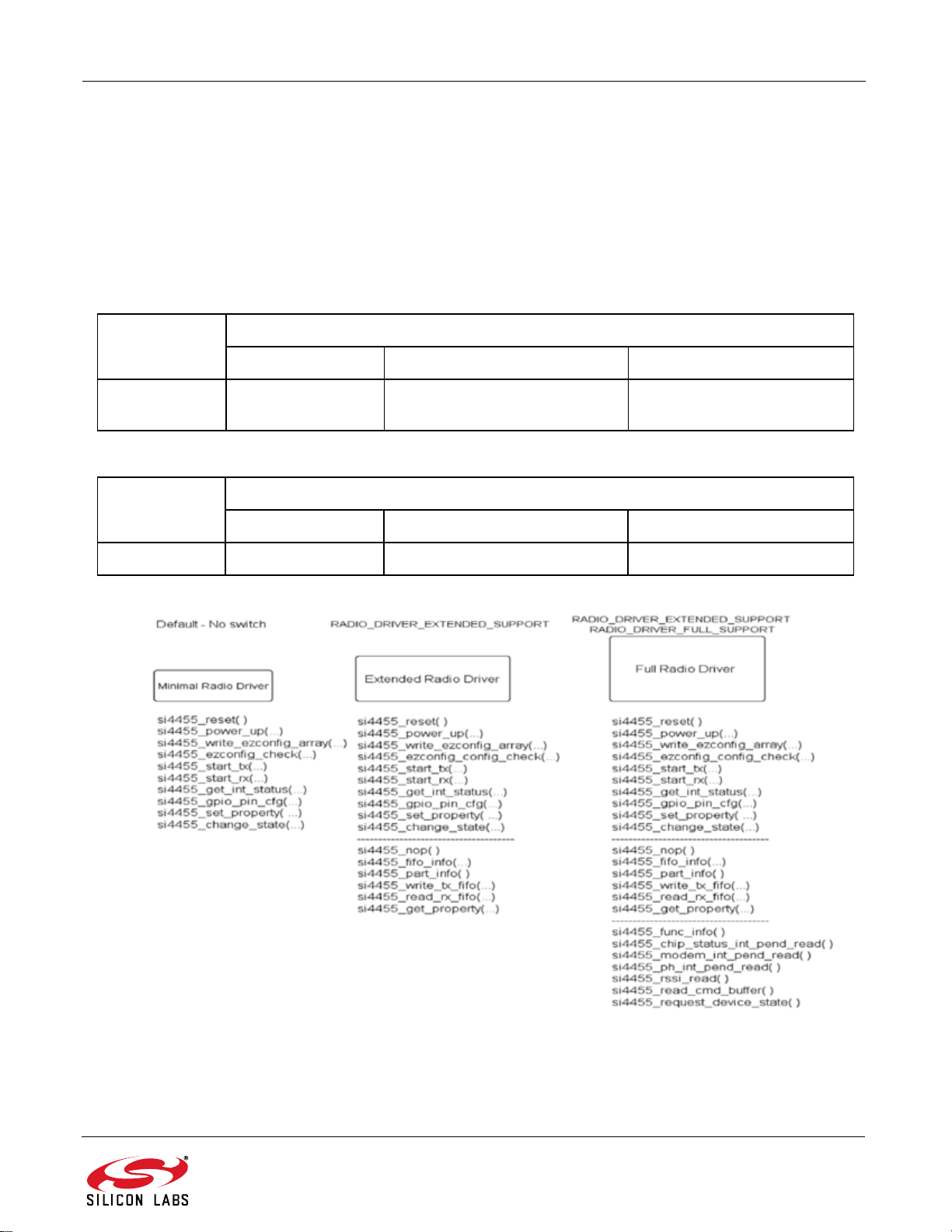
To optimize the code size of the common software modules and the example project, software switches are
introduced in the radio driver. By activating the switches, new functions can be added to the radio driver. If none of
the radio driver switches are defined at the beginning of the 'bsp.h' header file, then only the basic features are
used; however, this is a sufficient amount of features for all example projects to work. The rest of the features can
be added to the driver in two levels with the following switches:
RADIO_DRIVER_EXTENDED_SUPPORT
RADIO_DRIVER_FULL_SUPPORT
Table 8. Size Optimization Possibilities for Radio Driver
Driver Software Switch
Minimal Driver Extended Driver Full Driver
Radio default
Table 9. Size Comparison of Radio Driver
Driver Module size [byte]
Minimal Driver Extended Driver Full Driver
Radio 676 900 1042
RADIO_DRIVER_
EXTENDED_SUPPORT
RADIO_DRIVER_
FULL_SUPPORT
Figure 45. Usage of Radio Driver Switches
Rev 0.4 51
Page 52
AN692
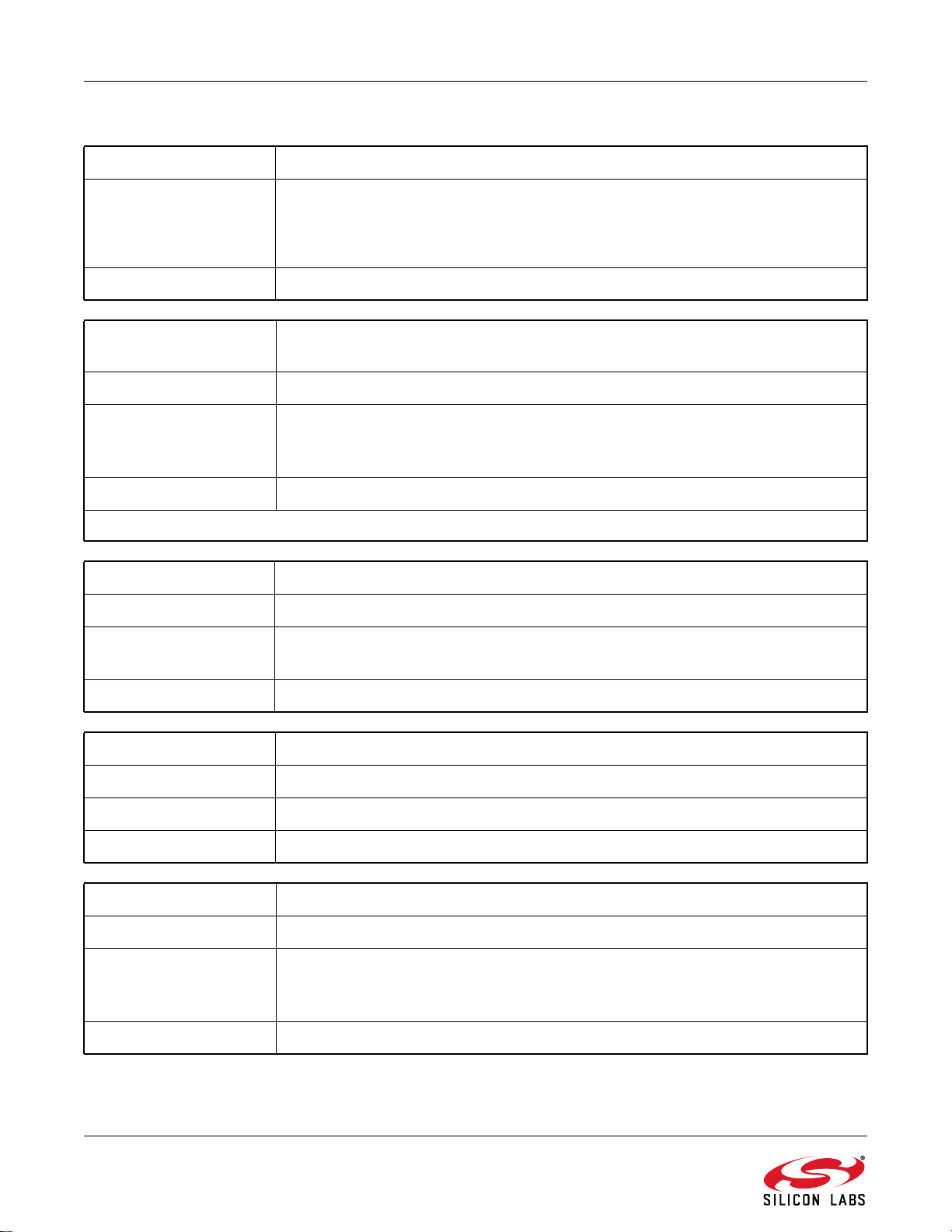
5.3.3. Minimal Radio Driver
Function Name: void si4455_reset(void);
Description: This functions is used to reset the si4455 radio by applying shutdown and releasing it.
After this function, si4455_boot should be called. You can check if POR has completed by waiting 5 ms or by polling GPIO 0, 2, or 3. When these GPIOs are high, it is
safe to call si4455_boot.
Return Value: None
Function Name: void si4455_power_up(U8 BOOT_OPTIONS, U8 XTAL_OPTIONS, U32 XO_-
FREQ);
Description: This function is used to initialize after powering up the radio chip.
Input Parameter(s): BOOT_OPTIONS : Patch mode selector
XTAL_OPTIONS : Select if TCXO is in use
XO_FREQ :Frequency of TCXO or external crystal oscillator in Hz
Return Value: None
Note: Before using this function, si4455_reset should be called.
Function Name: void si4455_write_ezconfig_array(U8 numBytes, U8* pEzConfigArray);
Description: This function can be used to configure the chip.
Input Parameter(s): numBytes : Data length to be loaded.
pEZConfigArray : Pointer to the data (U8*).
Return Value: None
Function Name: void si4455_ezconfig_check(U16 CHECKSUM);
Description: Check if the EZConfig array is sent correctly to the radio
Input Parameter(s): CHECKSUM : Checksum of the EZConfig array
Return Value: None
Function Name: void si4455_start_tx(U8 CHANNEL, U8 CONDITION, U16 TX_LEN);
Description: Sends START_TX command to the radio.
Input Parameter(s): CHANNEL : Channel number.
CONDITION : Start TX condition.
TX_LEN : Payload length (exclude the PH generated CRC).
Return Value: None
52 Rev 0.4
Page 53
AN692
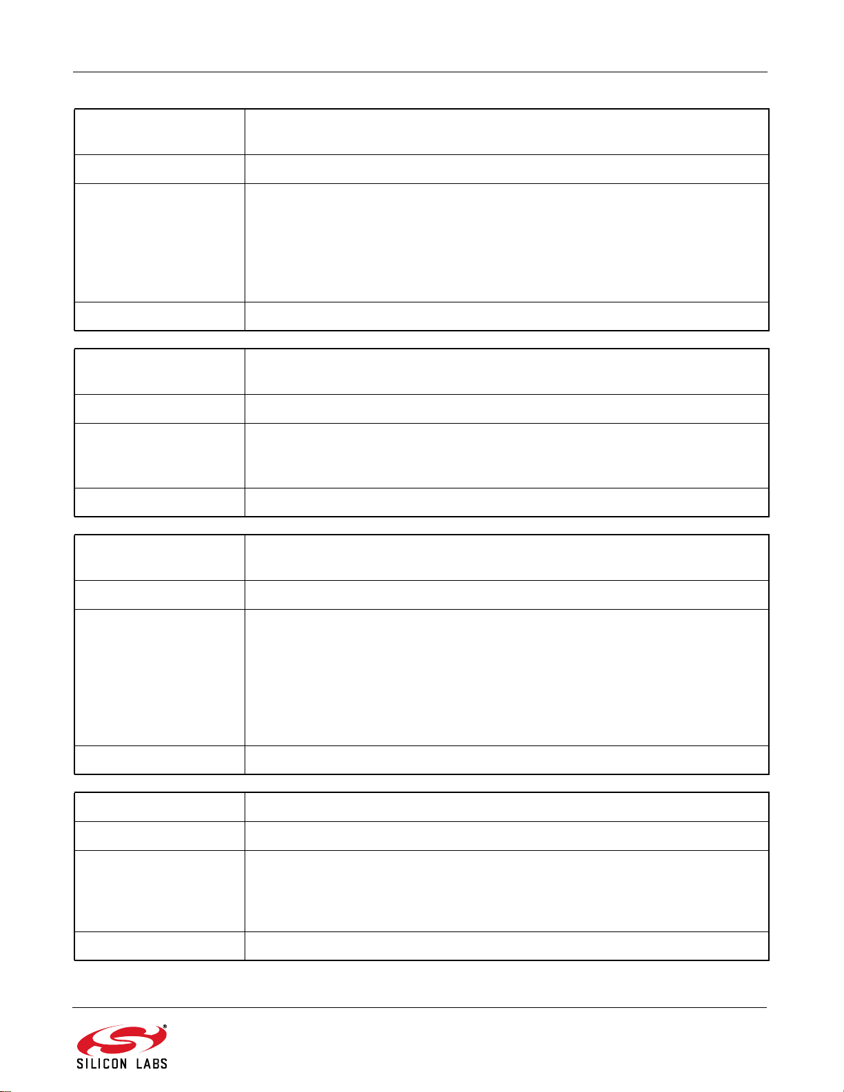
Function Name: void si4455_start_rx(U8 CHANNEL, U8 CONDITION, U16 RX_LEN, U8 NEX-
T_STATE1, U8 NEXT_STATE2, U8 NEXT_STATE3);
Description: Sends START_RX command to the radio.
Input Parameter(s): CHANNEL : Channel number.
CONDITION : Start RX condition.
RX_LEN : Payload length (exclude the PH generated CRC).
NEXT_STATE1 : Next state when Preamble Timeout occurs.
NEXT_STATE2 : Next state when a valid packet received.
NEXT_STATE3 : Next state when invalid packet received (e.g. CRC error).
Return Value: None
Function Name: void si4455_get_int_status(U8 PH_CLR_PEND,U8 MODEM_CLR_PEND, U8
CHIP_CLR_PEND);
Description: Get the Interrupt status/pending flags form the radio and clear flags if requested.
Input Parameter(s): PH_CLR_PEND : Packet Handler pending flags clear.
MODEM_CLR_PEND : Modem Status pending flags clear.
CHIP_CLR_PEND : Chip State pending flags clear.
Return Value: None
Function Name: void si4455_gpio_pin_cfg(U8 GPIO0, U8 GPIO1, U8 GPIO2, U8 GPIO3, U8 NIRQ,
U8 SDO, U8 GEN_CONFIG)
Description: Send GPIO pin config command to the radio and reads answer to Si446xCmd union.
Input Parameter(s): GPIO0 : GPIO0 configuration.
GPIO1 : GPIO1 configuration.
GPIO2 : GPIO2 configuration.
GPIO3 : GPIO3 configuration.
NIRQ : NIRQ configuration.
SDO : SDO configuration.
GEN_CONFIG : General pin configuration.
Return Value: None
Function Name: void si4455_set_property( U8 GROUP, U8 NUM_PROPS, U8 START_PROP, ... )
Description: Send SET_PROPERTY command to the radio.
Input Parameter(s): GROUP : Property group.
NUM_PROPS : Number of property to be set. The properties must be in ascending
order in their sub-property aspect. Max. 12 properties can be set in one command.
START_PROP : Start sub-property address.
Return Value: None
Rev 0.4 53
Page 54
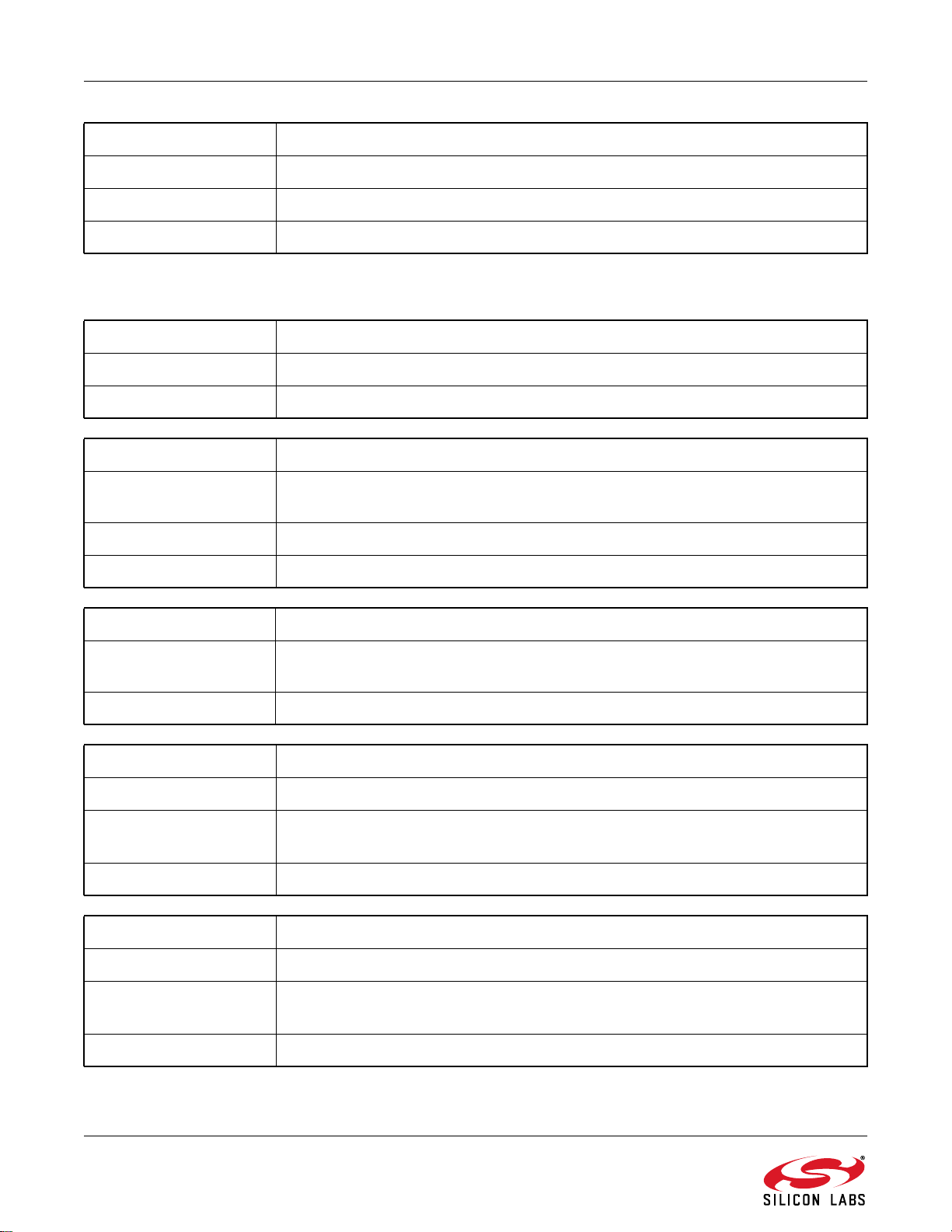
AN692
Function Name: void si4455_change_state(U8 NEXT_STATE1);
Description: Issue a change state command to the radio.
Input Parameter(s): NEXT_STATE1 : Next state
Return Value: None
5.3.4. Extended Radio Driver
Function Name: void si4455_nop(void)
Description: Sends NOP command to the radio. Can be used to maintain SPI communication.
Return Value: None
Function Name: void si4455_fifo_info(U8 FIFO)
Description: Send the FIFO_INFO command to the radio. Optionally resets the TX/RX FIFO.
Reads the radio response back Si4455Cmd union.
Input Parameter(s): FIFO : RX/TX FIFO reset flags.
Return Value: None
Function Name: void si4455_part_info(void)
Description: This function sends the PART_INFO command to the radio and receives the answer
Si4455Cmd union.
Return value: None
Function Name: void si4455_write_tx_fifo(U8 numBytes, U8* pTxData)
Description: The function can be used to load data into TX FIFO.
Input Parameter(s): numBytes : Data length to be load.
pTxData : Pointer to the data (U8*).
Return Value: None
Function Name: void si4455_read_rx_fifo(U8 numBytes, U8* pRxData)
Description: Reads the RX FIFO content from the radio.
Input Parameter(s): numBytes : Data length to be read.
pRxData : Pointer to the buffer location.
Return Value: None
54 Rev 0.4
Page 55
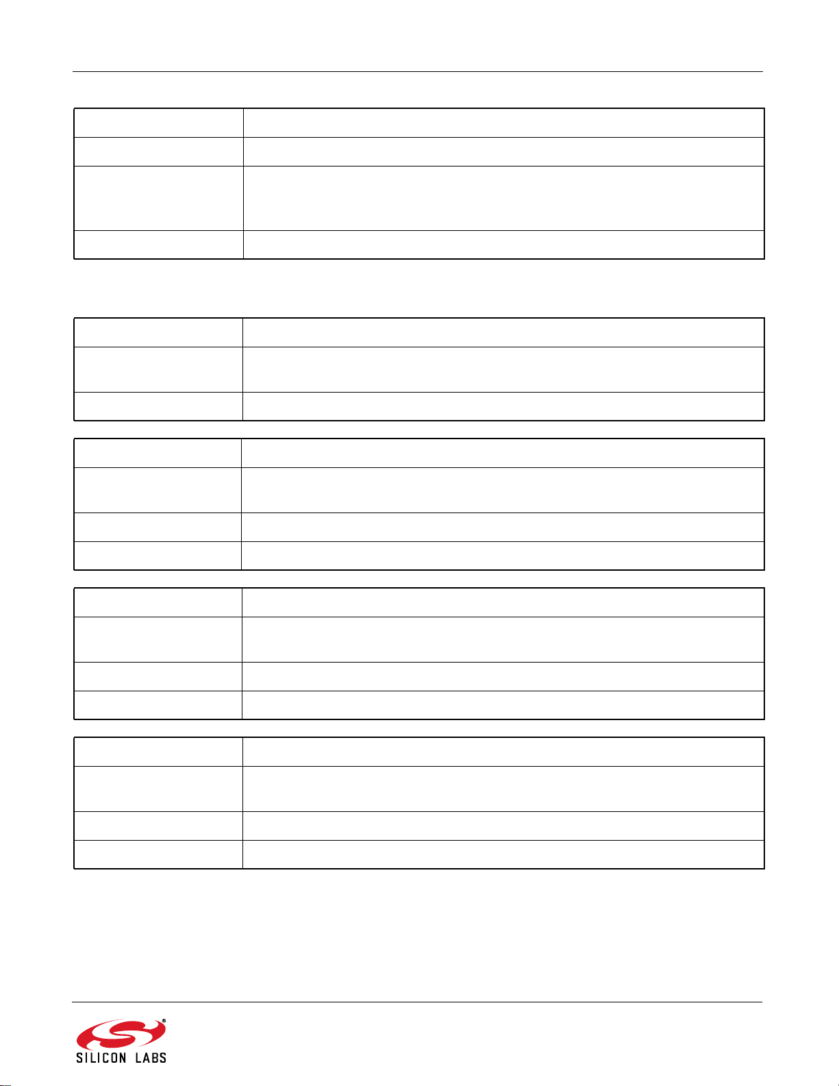
AN692
Function Name: void si4455_get_property(U8 GROUP, U8 NUM_PROPS, U8 START_PROP)
Description: Get property values from the radio. Reads them into Si4455Cmd union.
Input Parameter(s): GROUP : Property group number.
NUM_PROPS : Number of properties to be read.
START_PROP : Starting sub-property number.
Return Value: None
5.3.5. Full Radio Driver
Function Name: void si4455_func_info(void)
Description: Sends the FUNC_INFO command to the radio, then reads the response into
Si4455Cmd union.
Return Value: None
Function Name: void si4455_frr_a_read(U8 respByteCount)
Description: Returns the fast response registers (FRR) starting with FRR_A into Si4455Cmd
union.
Input Parameter(s): respByteCount : Data length to be read.
Return Value: None
Function Name: void si4455_frr_b_read(U8 respByteCount)
Description: Returns the fast response registers (FRR) starting with FRR_B into Si4455Cmd
union.
Input Parameter(s): respByteCount : Data length to be read.
Return Value: None
Function Name: void si4455_frr_c_read(U8 respByteCount)
Description: Returns the fast response registers (FRR) starting with FRR_C into Si4455Cmd
union.
Input Parameter(s): respByteCount : Data length to be read.
Return Value: None
Rev 0.4 55
Page 56
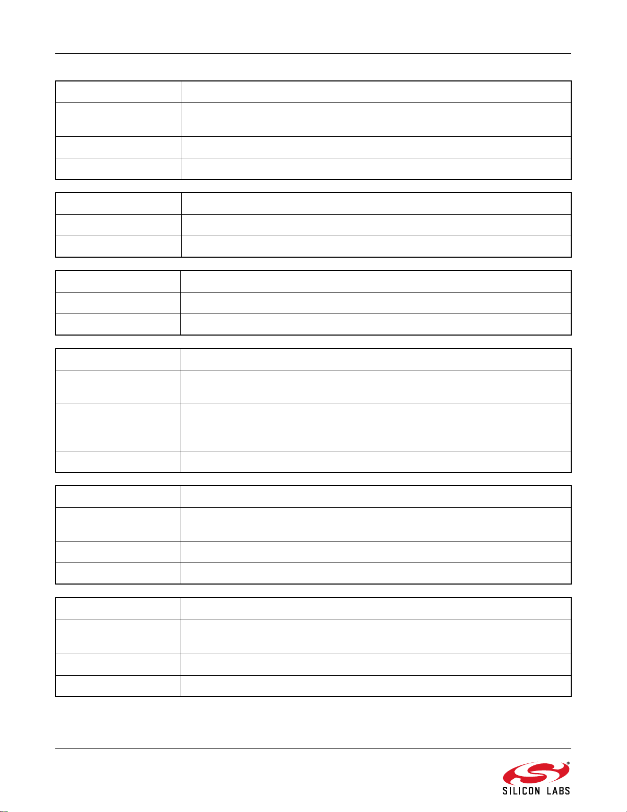
AN692
Function Name: void si4455_frr_d_read(U8 respByteCount)
Description: Returns the fast response registers (FRR) starting with FRR_D into Si4455Cmd
union.
Input Parameter(s): respByteCount : Data length to be read.
Return Value: None
Function Name: void si4455_read_cmd_buffer(void);
Description: Returns Clear to Send (CTS) value and the result of the previous command.
Return Value: None
Function Name: void si4455_request_device_state(void)
Description: Requests the current state of the device and lists pending TX and RX requests
Return Value: None
Function Name: void si4455_get_adc_reading(U8 ADC_EN, U8 ADC_CFG )
Description: Performs conversions using the Auxiliary ADC and returns the results of those con-
versions into Si4455Cmd union.
Input Parameter(s): ADC_EN : Defines sources to be converted.
ADC_CFG : Selects the rate of ADC conversion and attenuation factor to be internally
applied to the voltage on the GPIO pin.
Return Value: None
Function Name: void si4455_get_ph_status(U8 PH_CLR_PEND);
Description: Returns the interrupt status of the Packet Handler Interrupt Group into Si4455Cmd
union. Optionally clears pending flags.
Input Parameter(s): PH_CLR_PEND : Packet Handler pending flags to clear.
Return Value: None
Function Name: void si4455_get_modem_status( U8 MODEM_CLR_PEND );
Description: Returns the interrupt status of the Modem Interrupt Group into Si4455Cmd union.
Optionally clears pending flags.
Input Parameter(s): MODEM_CLR_PEND : Modem Status pending flags to clear.
Return Value: None
56 Rev 0.4
Page 57

AN692
Function Name: void si4455_get_chip_status( U8 CHIP_CLR_PEND );
Description: Returns the interrupt status of the Chip Interrupt Group into Si4455Cmd union.
Optionally clears pending flags.
Input Parameter(s): CHIP_CLR_PEND : Chip State pending flags to clear.
Return Value: None
Rev 0.4 57
Page 58
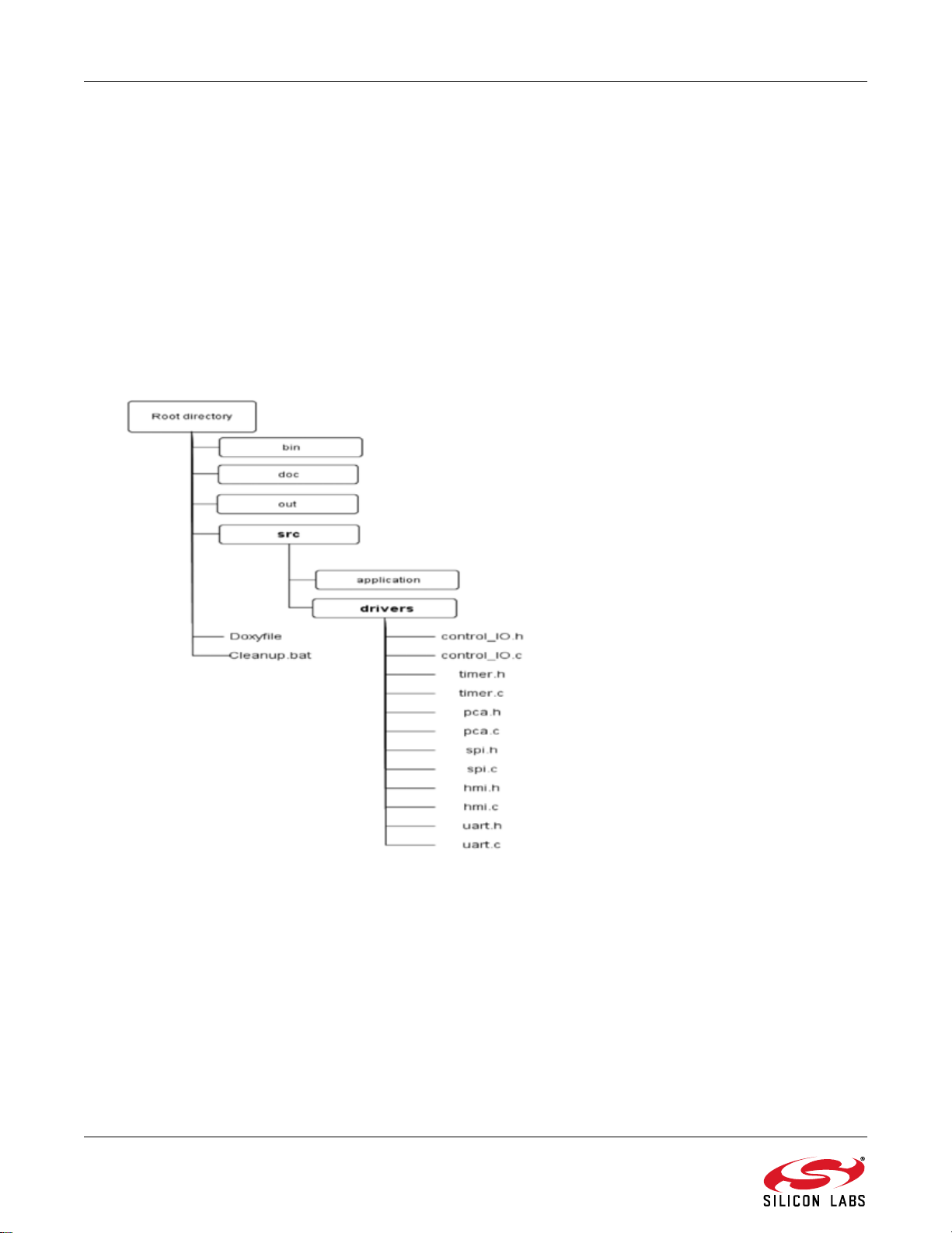
AN692
5.4. Common Software Modules
In the modules hierarchy, the common software modules (CSM) are located between the application and the
hardware layers.The CSM are a set of interfaces that enable control of various peripherals on modular HW
platforms. Registers can be initialized with pre-configured settings and peripherals can be enabled to start/stop
their own processing. The major tasks of these software modules are to initialize the hardware elements and
control its behaviors. The principle of their installation is to provide a façade for the upper layers. Functionally, the
User Application, at the top of the hierarchy, can be independent of the hardware and its logical operation can
remain unchanged even if the hardware has been modified later. It also can be adapted to any device without
encountering difficulties. All the modules in the following subsections except the human-machine interface module
are mainly responsible for handling the dedicated internal peripherals such as the IO, the timers, the SPI and the
PCA. The HMI holds them together so it gives a higher abstraction level to the User Application in the form of
handlers.
5.4.1. Common Software Modules Location
Figure 46. Location of the Common Software Modules
58 Rev 0.4
Page 59
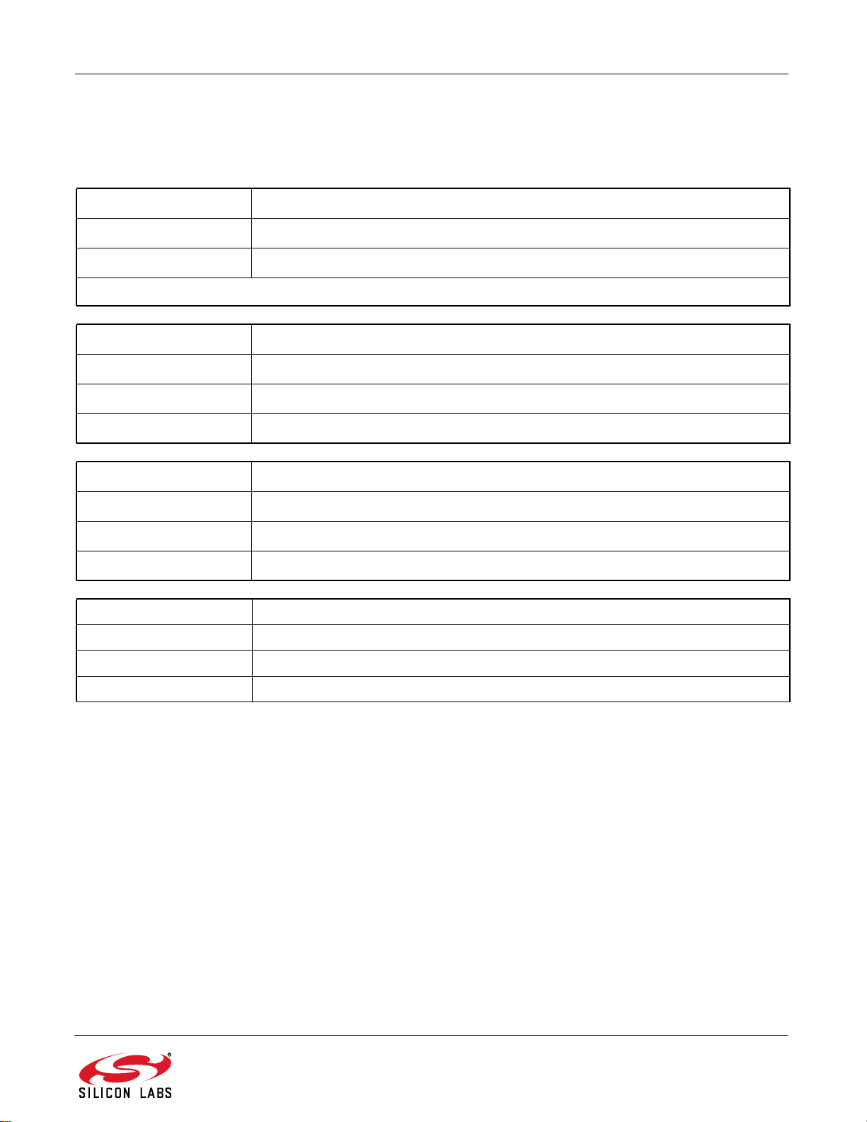
AN692
5.4.2. Input Output Control Module
The IO control-related source files, called 'control_IO.h' and 'control_IO.c', can be found in the /src/drivers/ folder.
The module handles the port initializations for the physical HW platform, e.g., LEDs, push-buttons, buzzer. It can
set the state of the LEDs and read the status of the selected push-buttons.
Function Name: void vCio_InitIO(void)
Description: This function is used to initialize specific IO port for LED & PB.
Return Value: None
Note: It has to be called from the initialization section.
Function Name:
Description:
Input Parameter(s):
Return Value:
Function Name: void vCio_ClearLed(U8 biLedNum)
Description: This function is used to switch the selected LED off.
Input Parameter(s): biLedNum : Number of the LED to be switched off (1 ... 4).
Return Value: None
Function Name: BIT gCio_GetPB(U8 biPbNum)
Description: This function is used to read the status of the selected push-button.
Input Parameter(s): biPbNum : Number of the push-button to be switched on (1 ... 4).
Return Value: State of the selected PB.
void vCio_SetLed(U8 biLedNum)
This function is used to switch the selected LED on.
biLedNum : Number of the LED to be switched on (1 ... 4).
None
Rev 0.4 59
Page 60
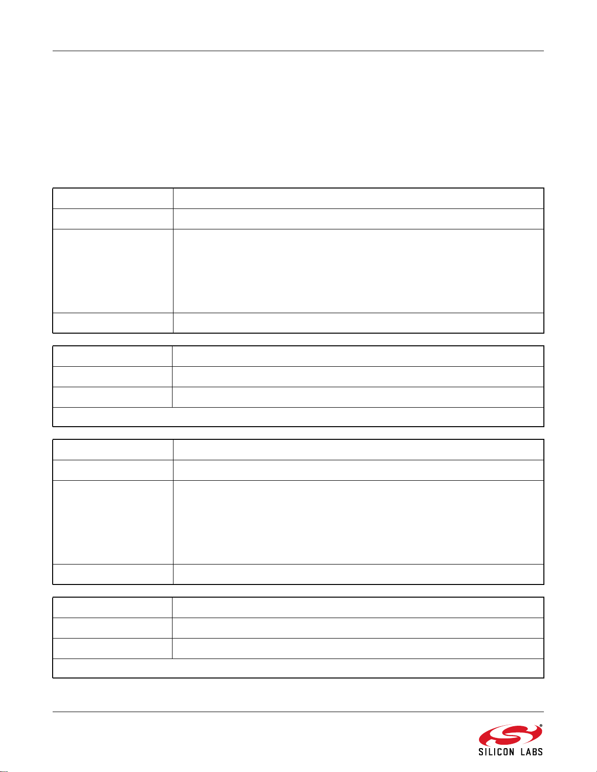
AN692
5.4.3. Timer Peripheral Module
The timer related source files, called ' timer.h' and 'timer.c', can be found in the /src/drivers/ folder. The module
handles two 16-bit timers, timer2 and timer3. The most accurate timing interval can be calculated from the
frequency of the system clock which is generally 24.5 MHz. External clock sources can be selected as timer input
and the required timing frequency can be adjusted thoroughly with several different prescalers. In general, the
timer settings belonging to the “heart-beat frequency” of 1 kHz (1 ms) are prepared. Using the timer with the 1 ms
settings, timeouts multiple of 1 ms can be easily implemented. Timer related operations can give possibilities to
start or stop counting. Additionally, interrupts can be generated when the low byte of the timer overflows. Timers
can also be checked whether get expired or not.
Function Name: void vTmr_StartTmr2(U8 biPrescaler, U16 wiPeriod, U8 biItEnable, U8 biExtClkSel)
Description: This function is used to start Timer 2 in the specified mode.
Input Parameter(s): biPrescaler : Prescaler value of timer
(use predefined constants: bTmr_Tmr2One_c, bTmr_Tmr2Both_c)
wwiPeriod : The duration of the timing
biItEnable : Enables timer IT if TRUE, disables it if FALSE
biExtClkSel External clock select
(use predefined constants: bTmr_TxXCLK_00_c etc.)
Return Value: None.
Function Name: BIT gTmr_Tmr2Expired(void)
Description: This function is used to check if Timer 2 is expired.
Return Value: True if timer is expired (also stops the timer).
Note: Function clears the IT status flag as well.
Function Name: void vTmr_StartTmr3(U8 biPrescaler, U16 wiPeriod, U8 biItEnable, U8 biExtClkSel)
Description: This function is used to start Timer 3 in the specified mode.
Input Parameter(s): biPrescaler : Prescaler value of timer
(use predefined constants: bTmr_Tmr3One_c, bTmr_Tmr3Both_c)
wwiPeriod : The duration of the timing
biItEnable : Enables timer IT if TRUE, disables it if FALSE
biExtClkSel : External clock select
(use predefined constants: bTmr_TxXCLK_00_c etc.)
Return Value: None
Function Name: BIT gTmr_Tmr3Expired(void)
Description: This function is used to check if Timer 3 is expired.
Return Value: True if timer is expired (also stops the timer).
Note: Function clears the IT status flag as well.
60 Rev 0.4
Page 61
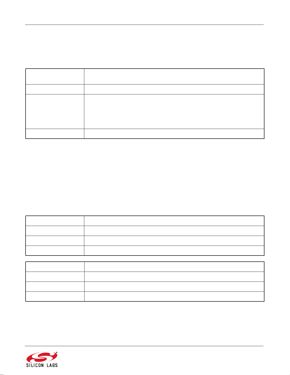
AN692
5.4.4. Programmable Counter Array Module
The PCA related source files, called 'pca.h' and 'pca.c', can be found in the /src/driver/ folder. The module initializes
the PCA to create beeping sounds on the buzzer. The time-base source of the PCA counter can be selected.
Interrupts can be generated when the lower byte of the counter overflows. PWM-mod cycle length can be also
selected to modify the frequency of the tweeting sound.
Function Name: void vPca_InitPcaTmr(U8 biPulseSelect, U8 biPcaTmrItEnable, U8 biCy-
cleLengthSelect)
Description: This function is used to start Timer 2 in the specified mode.
Input Parameter(s): biPulseSelect : Selects time-base source of PCA counter
(use predefined constants: bPca_PcaCps_000_c etc.)
biPcaTmrItEnable : Enables PCA timer IT if TRUE, disables it if FALSE
biCycleLengthSelect:PWM-mode cycle length select
(use predefined constants : bPca_PwmClsel_00_c etc.)
Return Value None
5.4.5. Serial Peripheral Interface Module
The SPI related source files, called 'spi.h' and 'spi.c', can be found in the /src/driver/ folder. This module is the most
essential, because it makes it possible to connect to the radio via the SPI bus. The radio can be controlled by its
built-in application programming interface. This control is based on sending commands towards the API and
receiving responses from the API. To enable the SPI interface, the SPI port must be enabled and associated to the
crossbar. The directions of the SCK, MISO, and MOSI ports have to be configured properly on the IO port. Finally,
the default states of the pins have to be set correctly. Since several devices can be connected to the same SPI bus,
the NSEL pin of the selected device is activated during communication. Since the commands to be sent to the API
are sequences of bytes, the module has to be able to send and receive continuous byte streams. There are some
cases when either reading a single byte directly from the MISO or writing specified number of bits directly to the
MOSI is necessary. In order to cover these kinds of cases, bitbang read/write methods have been also
implemented.
Function Name: U8 bSpi_ReadWriteSpi0(U8 biDataIn)
Description: This function is used to read/write one byte from/to SPI0.
Input Parameter(s): biDataIn : Data to be sent.
Return Value: Read value of the SPI port after writing on it.
Function Name: U8 bSpi_ReadWriteSpi1(U8 biDataIn)
Description: This function is used to read/write one byte from/to SPI1.
Input parameter(s): biDataIn : Data to be sent.
Return Value: Read value of the SPI port after writing on it.
Rev 0.4 61
Page 62
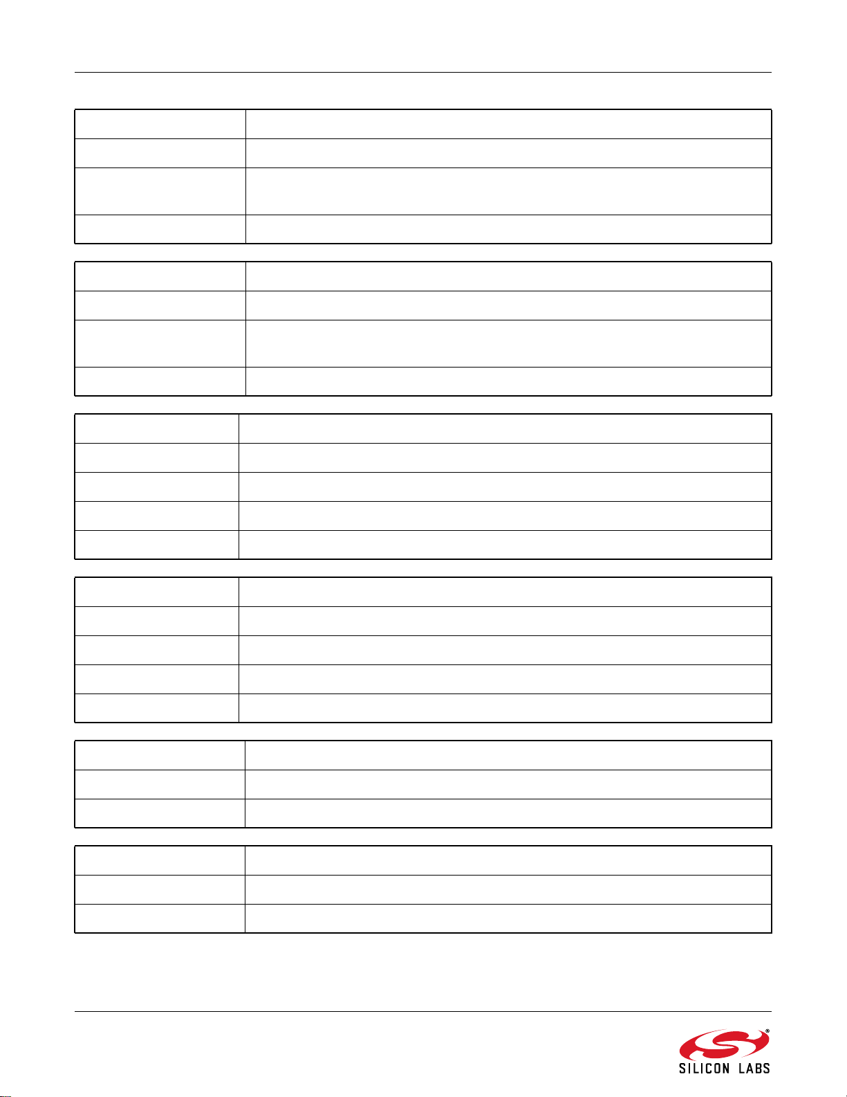
AN692
Function Name: void vSpi_WriteDataSpi0(U8 biDataInLength, U8 *pabiDataIn)
Description: This function is used to send data over SPI0 no response expected.
Input Parameter(s): biDataInLength : The length of the data.
*pabiDataIn : Pointer to the first element of the data.
Return Value: None
Function Name: void vSpi_WriteDataSpi1(U8 biDataInLength, U8 *pabiDataIn)
Description: This function is used to send data over SPI1 no response expected.
Input Parameter(s): biDataInLength : The length of the data.
*pabiDataIn : Pointer to the first element of the data.
Return Value: None
Function Name: void vSpi_ReadDataSpi0(U8 biDataOutLength, U8 *paboDataOut)
Description: This function is used to read data from SPI0.
Input Parameter(s): biDataOutLength :The length of the data.
Output Parameters(s): *paboDataOut : Pointer to the first element of the response.
Return Value: None
Function Name: void vSpi_ReadDataSpi1(U8 biDataOutLength, U8 *paboDataOut)
Description: This function is used to read data from SPI1.
Input Parameter(s): biDataOutLength : The length of the data.
Output Parameters(s): *paboDataOut : Pointer to the first element of the response.
Return Value: None
Function Name: void vSpi_EnableSpi0(void)
Description: This function is used to enable SPI0 and associate to XBAR.
Return Value: None
Function Name: void vSpi_EnableSpi1(void)
Description: This function is used to enable SPI1 and associate to XBAR.
Return Value: None
62 Rev 0.4
Page 63
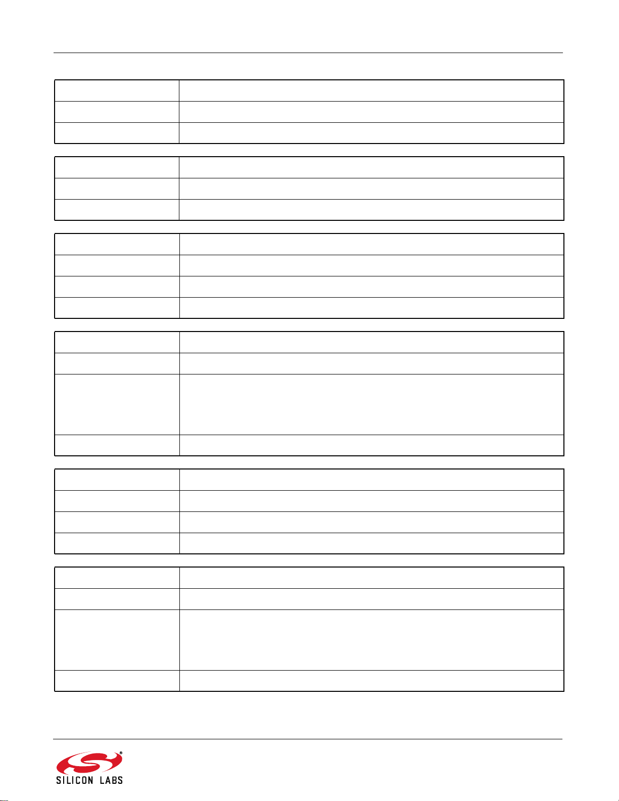
Function Name: void vSpi_DisableSpi0(void)
Description: This function is used to disable SPI0 and disconnect from XBAR.
Return Value: None
Function Name: void vSpi_DisableSpi1(void)
Description: This function is used to disable SPI1 and disconnect from XBAR.
Return Value: None
Function Name: void vSpi_ClearNselSpi0(U8 biSelectDevice)
Description: This function is used to pull down nSEL of the selected device on SPI0.
Input Parameter(s): biSelectDevice Selected device
Return Value: None
AN692
Function Name: void vSpi_ClearNselSpi1(U8 biSelectDevice)
Description: This function is used to pull down nSEL of the selected device on SPI1.
Input Parameter(s): biSelectDevice Selected device
0 - DUT
2 - EEPROM
3 - MCU2
Return Value: None
Function Name: void vSpi_SetNselSpi0(U8 biSelectDevice)
Description: This function is used to pull up nSEL of the selected device on SPI0.
Input Parameter(s): biSelectDevice : Selected device
Return Value: None
Function Name: void vSpi_SetNselSpi1(U8 biSelectDevice)
Description: This function is used to pull up nSEL of the selected device on SPI1.
Input Parameter(s): biSelectDevice: Selected device
0 - DUT
2 - EEPROM
3 - MCU2
Return Value: None
Rev 0.4 63
Page 64
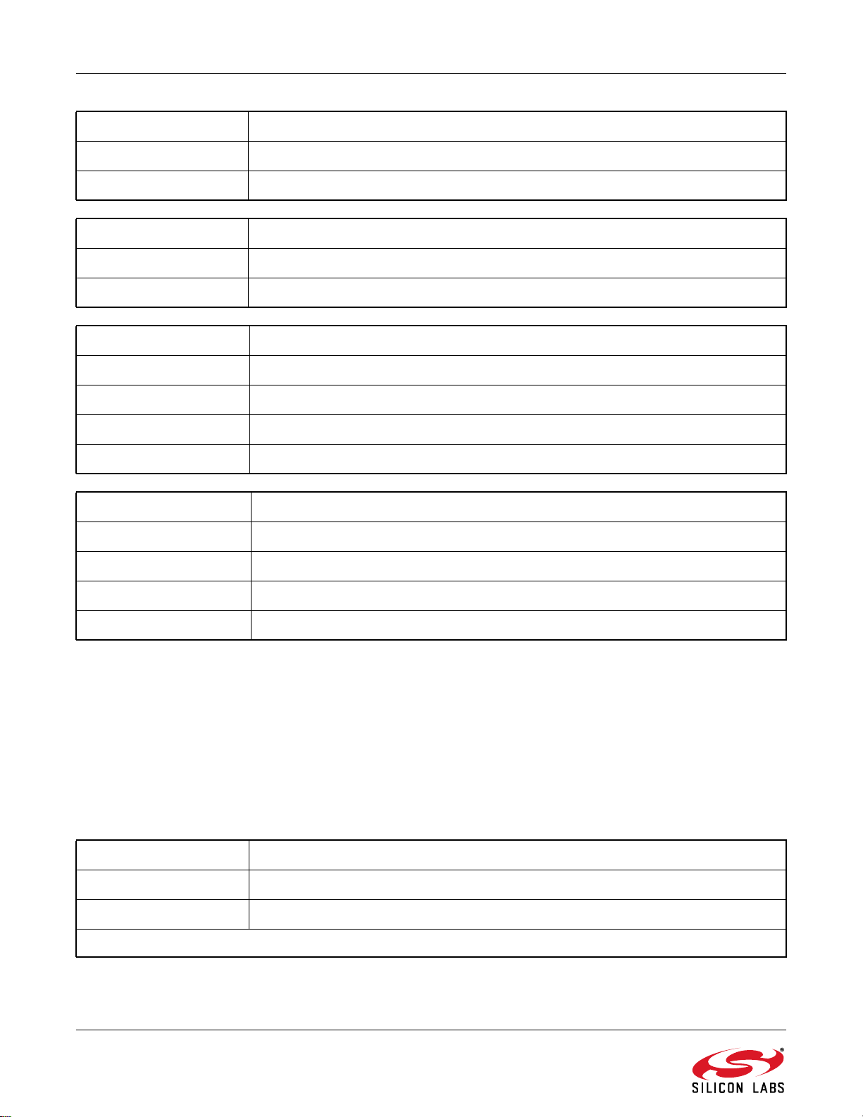
AN692
Function Name: U8 bSpi_ReadByteBitbangSpi0(void)
Description: This function is used to read one byte from SPI0 using bitbang method.
Return Value: Read byte
Function Name: U8 bSpi_ReadByteBitbangSpi1(void)
Description: This function is used to read one byte from SPI1 using bitbang method.
Return Value: Read byte
Function Name: void vSpi_WriteBitsBitbangSpi0(U8 biDataIn, U8 biNumOfBits)
Description: This function is used to write specified number of bits to SPI0 using bitbang method.
Input Parameter(s): biDataIn : Input byte of data bits
Output Parameters(s): biNumOfBits : Number of bits to be written to SPI
Return Value: None
Function Name: void vSpi_WriteBitsBitbangSpi1(U8 biDataIn, U8 biNumOfBits)
Description: This function is used to write specified number of bits to SPI1 using bitbang method.
Input Parameter(s): biDataIn : Input byte of data bits
Output Parameters(s): biNumOfBits : Number of bits to be written to SPI
Return Value: None
5.4.6. Human Machine Interface Module
The HMI related source files, called 'hmi.h' and 'hmi.c', can be found in the /src/driver/ folder. In order to use this
module, the required handlers need to be initialized at the very beginning of the program. Checking the status of
the various hardware components require a common cyclic mechanism. A 1 ms interrupt based cycle must be
running in the background to serve the different handlers. Using the LED handler, states of LEDs can be set and
cleared either separately or together.
The status of the push-buttons can be read by using the button handler. Even if more button events have happened
simultaneously, they can be stored to be handled later. The last pushed button event is always available first
amongst the unhandled events. Using the buzzer related sub-interface, the state of the buzzer can be changed to
the required one.
Function Name: void vHmi_InitLedHandler(void)
Description: This function is used to initialize the LED handler.
Return Value: None
Note: It has to be called from the initialization section. Re-initialization of LED Handler supported by the extended HMI driver
64 Rev 0.4
Page 65
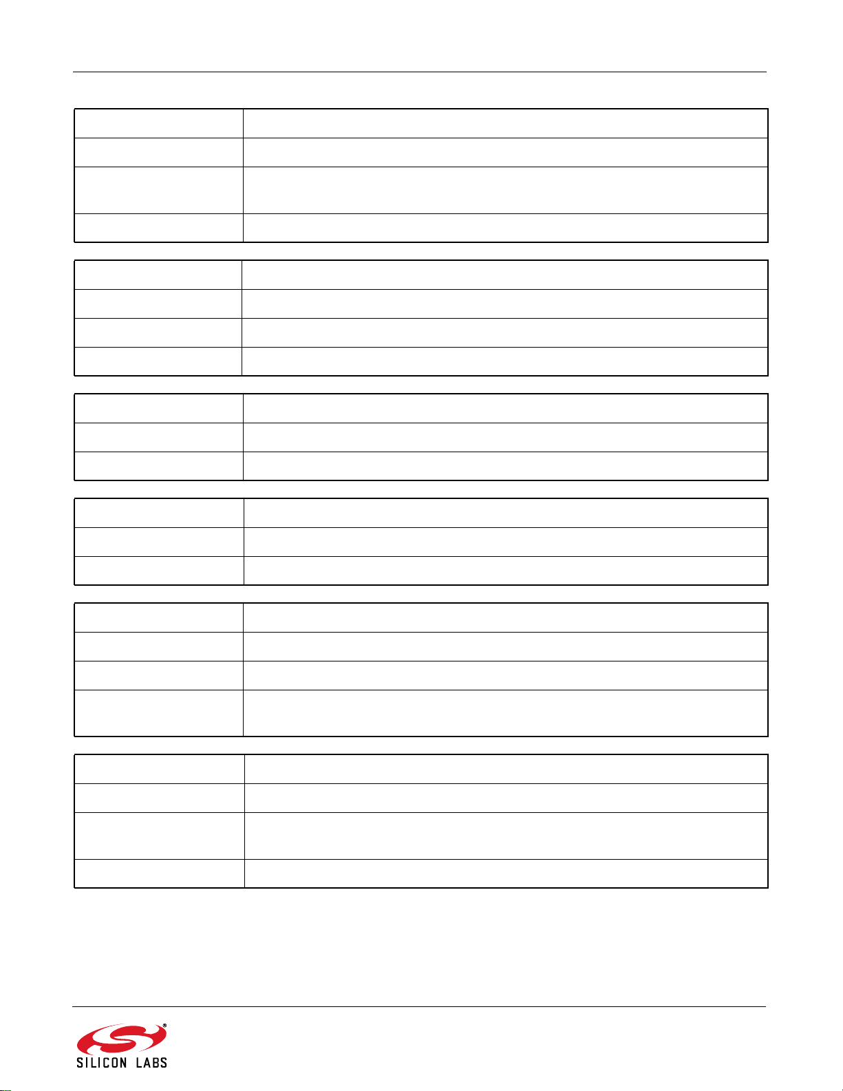
AN692
Function Name: void vHmi_ChangeLedState(eHmi_Leds qiLed, eHmi_LedStates qiLedState)
Description: This function is used to change state of selected LED.
Input Parameter(s): qiLed : LED to change its state
qiLedState : New state of qiLed
Return Value: None
Function Name: void vHmi_ChangeAllLedState(eHmi_LedStates qiLedState)
Description: This function is used to change state of all LEDs.
Input Parameter(s): qiLedState : New state of all the LEDs
Return Value: None
Function Name: void vHmi_ClearAllLeds(void)
Description: This function is used to force all LEDs to off immediately.
Return Value: None
Function Name: void vHmi_LedHandler(void)
Description: This function is used to handle LED management.
Return Value: None
Function Name: void vHmi_InitPbHandler(void)
Description: This function is used to initialize push-button handler.
Return Value: None
Note: It has to be called from the initialization section
Re-initialization of LED Handler supported by the extended HMI driver.
Function Name: BIT gHmi_PbIsPushed(U8 *boPbPushTrack, U16 *woPbPushTime)
Description: This function is used to check if any of the push-buttons are pushed.
Output Parameter(s): *boPbPushTrack : Read value of pushed button.
*woPbPushTime : Push time of pushed button.
Return Value: Pushed state of push-buttons
Rev 0.4 65
Page 66
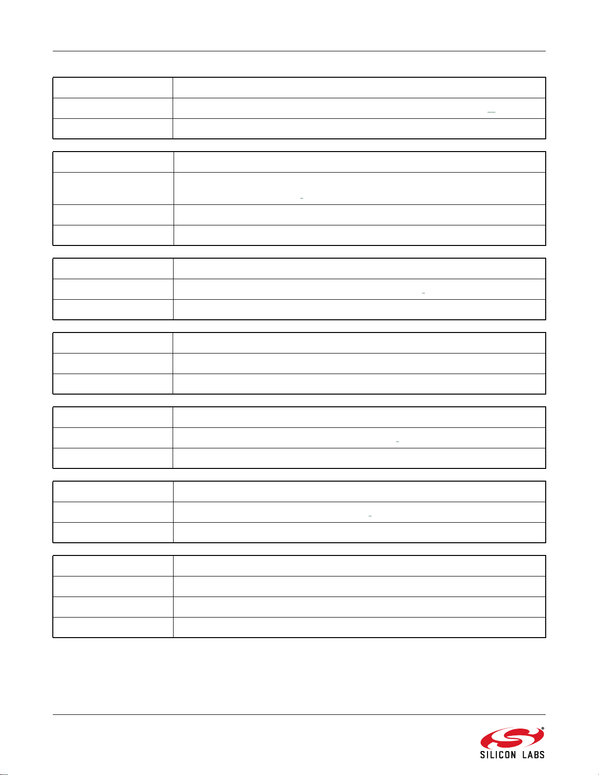
AN692
Function Name: BIT gHmi_IsPbUnHandled(void)
Description: This function is used to check if there are unhandled push-buttons events.
Return Value: True if there is unhandled push-button event.
Function Name: U8 bHmi_PbGetLastButton(U16 *woPbPushTime)
Description: This function is used to read last pushed button(s), push track holder is erased if but-
ton(s) were already released
Output Parameter(s): *woPbPushTime : Push time of pushed button
Return Value: Push track holder of last pushed button(s)
Function Name: void vHmi_PbHandler(void)
Description: This function is used to handle push-button management.
Return Value: None
.
Function Name: void vHmi_ShowPbOnLeds(void)
Description: This function is used to show the actual state of the push-buttons on the LEDs.
Return Value: None
Function Name: BIT gHmi_SwStateHandler(void)
Description: This function is used to handle switch state change.
Return Value: True if state of switches has changed
Function Name: U8 bHmi_GetSwState(void)
Description: This function is used to handle give the state.
Return Value: State
Function Name: void vHmi_InitBuzzer(void)
Description: This function is used to initialize the buzzer operation.
Return Value: None
Note: It has to be called from the initialization section
66 Rev 0.4
Page 67
AN692
Function Name: void vHmi_ChangeBuzzState(eHmi_BuzzStates qiBuzzState)
Description: This function is used to change the state of the buzzer.
Input Parameter(s): qiBuzzState : New state of the buzzer
Return Value: None
Function Name: void vHmi_BuzzHandler(void)
Description: This function is used to handle buzzer management.
Return Value: None
5.4.7. UART Interface Module
The UART related source files, called 'uart.h' and 'uart.c', can be found in the /src/driver/ folder. In order to use this
module, the functionality needs to be initialized at the very beginning of the program.
Bytes can be sent and received as well and the functionality uses the uart interrupt service routine.
Function Name: U8 Comm_IF_RecvUART(U8 * byte)
Description: This function is used to receive bytes from UART.
Output Parameter(s): *byte Pointer to the first element of the incoming data
Return Value: True if there is an incoming data otherwise FALSE
Function Name: U8 Comm_IF_SendUART(U8 byte)
Description: This function is used to send bytes through UART.
Input Parameter(s): byte : data to be sent
Return Value: True if sending data completed successfully otherwise FALSE
Function Name: void Comm_IF_EnableUART(void)
Description: Enable and set the UART0 peripheral
Return Value: None
Rev 0.4 67
Page 68
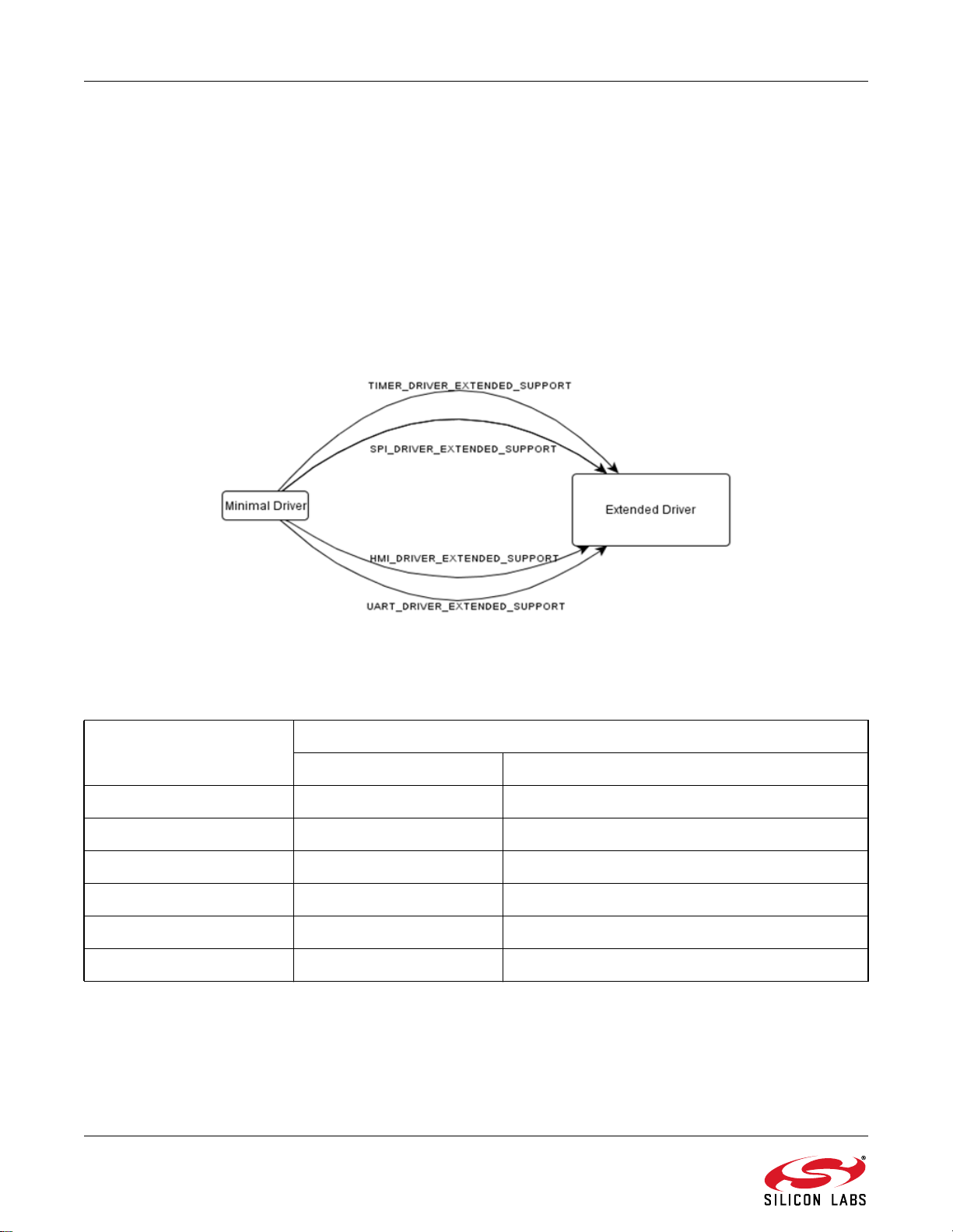
AN692
5.4.8. Size Optimization of the Common Software Modules
To optimize the code size of the common software modules as well as the example source codes, software
switches must be introduced in almost every module. By enabling these switches, new functions can be added to
the whole project to compile. If the switch is not defined at the beginning of the 'bsp.h' header file, then only the
basic features can be used. It is barely sufficient for most of the example codes.
The rest of the module's features can be added to the project by defining the following switches:
TIMER_DRIVER_EXTENDED_SUPPORT
SPI_DRIVER_EXTENDED_SUPPORT
HMI_DRIVER_EXTENDED_SUPPORT
UART_DRIVER_EXTENDED_SUPPORT
The control_IO and PCA modules are quite simple, so there is no need to use driver extension in these cases.
Figure 47. Usage of Software Switches
Table 10 shows which module can support the driver expansion feature:
Table 10. Size Optimization Possibilities for Common Software Module
Common Software Module Software Switch
Minimal Driver Extended Driver
Control IO default Not supported
Timer default TIMER_DRIVER_EXTENDED_SUPPORT
PCA default Not supported
SPI default SPI_DRIVER_EXTENDED_SUPPORT
HMI default HMI_DRIVER_EXTENDED_SUPPORT
UART default UART_DRIVER_EXTENDED_SUPPORT
68 Rev 0.4
Page 69
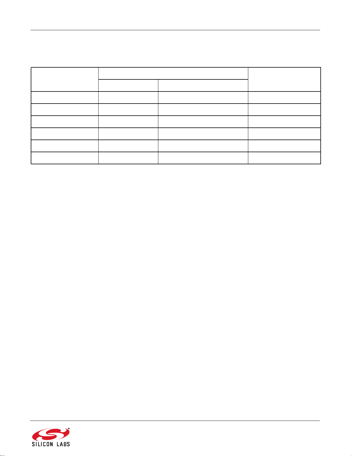
Table 11 shows the comparison between the modules' sizes:
Table 11. Size Comparison of Common Software Module
AN692
Common Software
Module
Minimal Driver Extended Driver
Control IO 60 Not supported -
Timer 60 146 58
PCA 29 Not supported -
SPI 127 252 49
HMI 698 1295 46
UART 49 246 80
Module Code Size [Byte] Size Optimization
[%]
Rev 0.4 69
Page 70
Simplicity Studio
One-click access to MCU tools,
documentation, software, source
code libraries & more. Available
for Windows, Mac and Linux!
www.silabs.com/simplicity
MCU Portfolio
www.silabs.com/mcu
Disclaimer
Silicon Laboratories intends to provide customers with the latest, accurate, and in-depth documentation of all peripherals and modules available for system and software implementers
using or intending to use the Silicon Laboratories products. Characterization data, available modules and peripherals, memory sizes and memory addresses refer to each specific
device, and "Typical" parameters provided can and do vary in different applications. Application examples described herein are for illustrative purposes only. Silicon Laboratories
reserves the right to make changes without further notice and limitation to product information, specifications, and descriptions herein, and does not give warranties as to the accuracy
or completeness of the included information. Silicon Laboratories shall have no liability for the consequences of use of the information supplied herein. This document does not imply
or express copyright licenses granted hereunder to design or fabricate any integrated circuits. The products must not be used within any Life Support System without the specific
written consent of Silicon Laboratories. A "Life Support System" is any product or system intended to support or sustain life and/or health, which, if it fails, can be reasonably expected
to result in significant personal injury or death. Silicon Laboratories products are generally not intended for military applications. Silicon Laboratories products shall under no
circumstances be used in weapons of mass destruction including (but not limited to) nuclear, biological or chemical weapons, or missiles capable of delivering such weapons.
Trademark Information
Silicon Laboratories Inc., Silicon Laboratories, Silicon Labs, SiLabs and the Silicon Labs logo, CMEMS®, EFM, EFM32, EFR, Energy Micro, Energy Micro logo and combinations
thereof, "the world’s most energy friendly microcontrollers", Ember®, EZLink®, EZMac®, EZRadio®, EZRadioPRO®, DSPLL®, ISOmodem ®, Precision32®, ProSLIC®, SiPHY®,
USBXpress® and others are trademarks or registered trademarks of Silicon Laboratories Inc. ARM, CORTEX, Cortex-M3 and THUMB are trademarks or registered trademarks of
ARM Holdings. Keil is a registered trademark of ARM Limited. All other products or brand names mentioned herein are trademarks of their respective holders.
Silicon Laboratories Inc.
400 West Cesar Chavez
Austin, TX 78701
USA
SW/HW
www.silabs.com/simplicity
Quality
www.silabs.com/quality
Support and Community
community.silabs.com
http://www.silabs.com
 Loading...