

MODEM-DK
EMBEDDED MODEM DEVELOPMENT KIT USER’S GUIDE
1. Kit Contents
The Embedded Modem Development Kit contains the following items:
• C8051F120 Target Board
• AB3 Modem Adapter Board
• Si2457FT18-EVB Modem Board
• Silicon Laboratories Evaluation Kit IDE and Product Information CD-ROM. CD content includes the following:
• Silicon Laboratories Integrated Development Environment (IDE)
• Keil Software 8051 Development Tools (evaluation assembler, linker and ‘C’ compiler)
• Source code examples and register definition files
• Documentation
• TCP/IP Configuration Wizard
• Embedded Modem Development Kit User’s Guide (this document)
• AC to DC Power Adapter
• USB Debug Adapter (USB to Debug Interface)
• USB Cable
2. Kit Overview
This Embedded Modem Development kit provides a means to develop real-world embedded modem applications
based on the CMX Micronet™ protocol stack running on Silicon Laboratories MCU devices. See application note
“AN237: TCP/IP Library Programmer’s Guide” for detailed information about the TCP/IP stack. The kit includes
three development boards along with the Silicon Laboratories TCP/IP Configuration Wizard and Integrated
Development Environment (IDE) to expedite embedded modem designs. Section 3 takes the designer through an
example illustrating each of the steps to create an application using the included software.
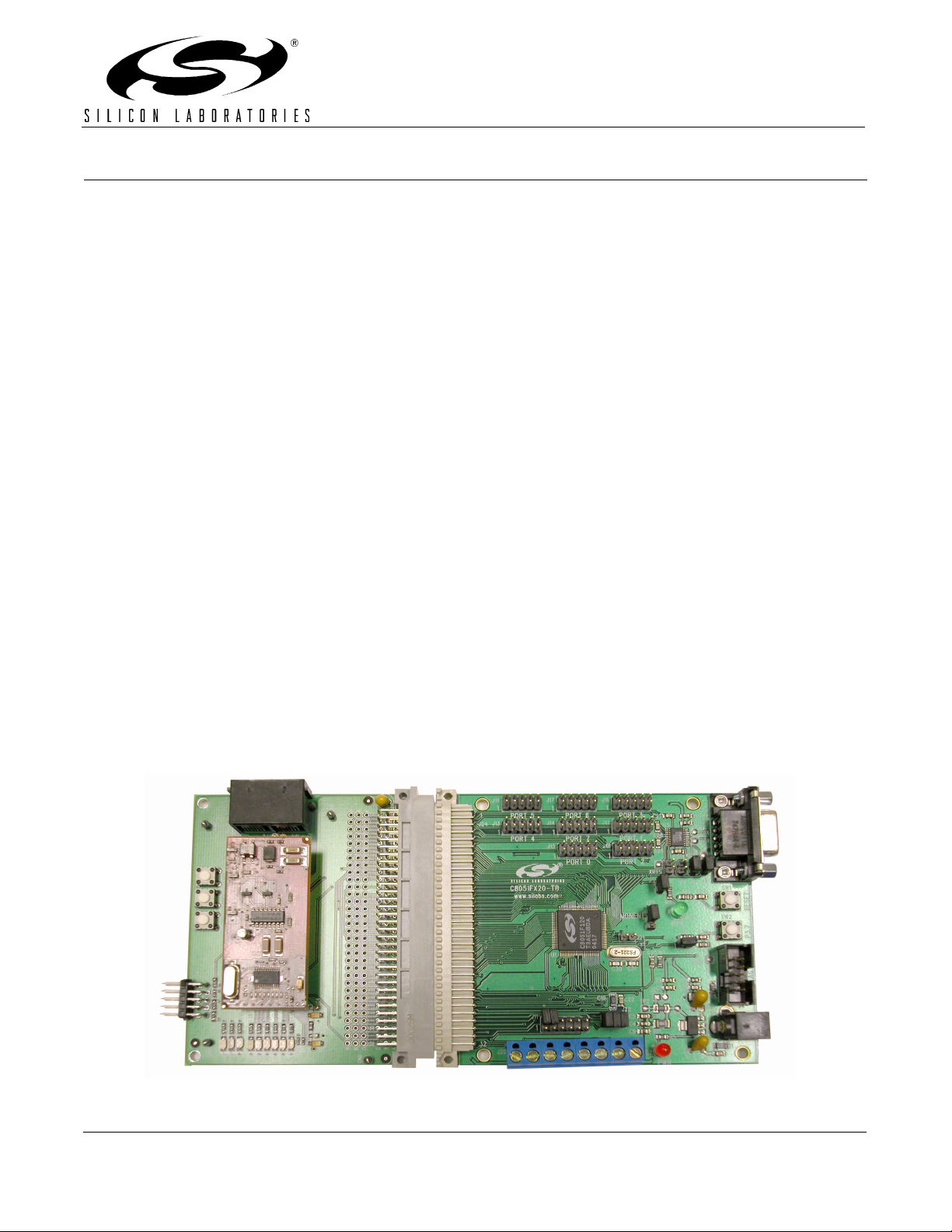
A C8051F120 Target Board, an AB3 Modem Adapter board, and a Si2457FT18-EVB Modem Board are included in
the Embedded Modem Development kit. These boards are shown in Figure 1. The C8051F120 Target Board is a
Silicon Laboratories standard development board featuring the 100 MIPs, 8051-based C8051F120 MCU. The AB3
Modem Adaptor Board connects the C8051F120 board to the Si2457 modem chipset board, the Si2457FT18-EVB.
Figure 1. Embedded Modem Development Kit Hardware Overview
Rev. 0.2 9/06 Copyright © 2006 by Silicon Laboratories MODEM-DK
MODEM-DK
3. Development Kit Embedded Modem Demonstration
The example detailed below describes the steps necessary to run a simple demonstration. This example steps
through hardware setup and code configuration using the TCP/IP Configuration Wizard and the Silicon
Laboratories IDE to create and debug an example ping application.
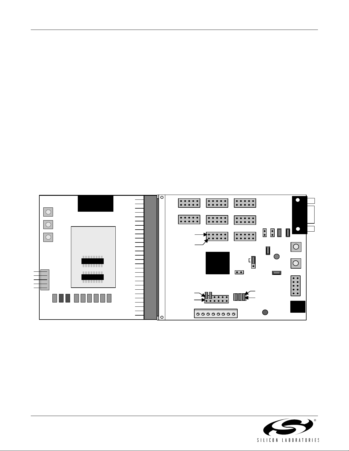
3.1. Hardware Setup
Connect the hardware included with the kit according to the instructions listed below. Diagrams of the hardware
setup are shown in Figure 2 and Figure 3.
1. Connect the Si2457FT18-EVB Modem Board to the AB3 Modem Adapter Board at JP1 and JP2.
2. Connect the AB3 Modem Adapter Board to the C8051F120 Target Board at J24.
3. Using the ribbon cable, connect the USB Debug Adapter to the C8051F120 Target Board at the JTAG
header.
4. Connect one end of the provided USB cable to any available USB port on the PC.
5. Connect the other end of the USB cable into the USB connector on the USB Debug Adapter.
6. Connect the ac/dc Power Adapter to the C8051F120 Target Board at P1. This connection should power
the boards. Power is indicated by the "PWR" LED.
J8J10 J6
P1.6
J1
J5
J9
J4
P1
RESET
P3.7
JTAG
J24
Port 3Port 6Port 5
RJ11
Si2457FT1-EVB
SW1 SW2 SW3
JP2
Modem Board
JP4
JP1
AB3 Modem Adapter Board
RTS
ESC
LED1
LED2
RXD
DCD
RI
TXD
CTS
Port 4
Pin 2
Pin 1
C8051F120
Target Board
Pin 2
Pin 1
J20
Port 7
Port 0 Port 2
C8051F12x
J11
MONEN
J21
J22
Port 1
J3
J23
Pin 2
Pin 1
PWR
Figure 2. Embedded Modem Demo Board Connections
2 Rev. 0.2
MODEM-DK
Si2457FT1
-EVB
Modem
Board
C8051F120
Target Board
AB3 Modem Adapter Board
JTAG
Ribbon
Cable
AC / DC
Adapter
USB
Debug
Adapter
PC
USB
Cable
USB Port
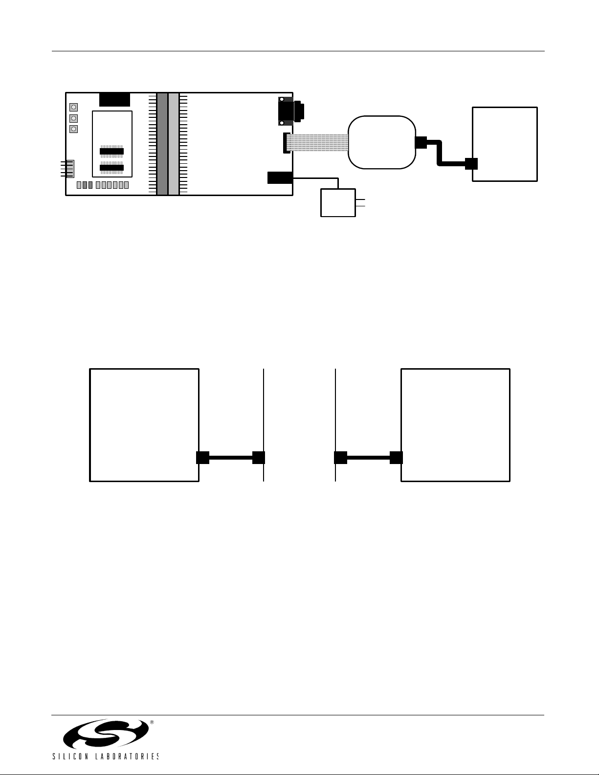
Figure 3. Embedded Modem Demo Debug Connections
3.2. Phone Line Hardware Setup
Connect the phone lines and modems according to the instructions listed below. A diagram of the phone line setup
is shown in Figure 4.
1. Connect a phone cable from the target PC and modem to a phone line simulator or a phone line outlet.
2. Connect a phone cable from the AB3 Modem Adapter Board at the RJ11 connector to the phone line
simulator or a phone line outlet.
PC
+
Modem
Connector
Modem
Phone
Cable
Phone Line
Simulator
Or
Phone Line
Outlets
Phone
Cable
Embedded Modem
Development Kit
including
Si2457 ISOModem
Modem
Connector
®
Figure 4. Embedded Modem Demo Phone Line Connections
3.3. Software Installation
Install the software included with the Embedded Modem Development kit according to the instructions below.
1. Place the Embedded Modem Development Kit CD-ROM into the PC for application install.
2. An installation dialogue box will appear. Click the Install Development Tools button.
3. Follow the installation prompts to install the development tools. The Silicon Laboratories IDE will be
installed by default in the “C:\SiLabs\MCU” directory, the Embedded Modem examples will be installed by
default in the “C:\SiLabs\MCU\Examples\Modem” directory, and the TCP/IP Configuration Wizard will be
installed by default in the “C:\SiLabs\MCU\TCP-IP Config” directory. In addition, shortcuts to the applications will be placed in the Start→Programs menu.
Rev. 0.2 3

MODEM-DK
3.4. Configuring PC Modem Settings
The target PC and modem must be configured to receive communications from the Si2457 in the Embedded
Modem Development Kit. Follow the steps below to configure the PC.
1. Open the Network Connections window. Links can be found in the Start menu or the Control Panel.
2. Select Create a New Connection from the File menu in the Network Connections window.
3. The New Connection Wizard will open. Click the Next button.
4. Select the Set up an advanced connection option. Click the Next button. (This window might appear with
all operating systems.)
5. Select the Accept incoming connections option. Click the Next button.
6. The next window should show all of the available devices on the PC. Check the modem that will be used
for the demo.
7. The Incoming Virtual Private Network (VPN) Connection window does not require any selections. Click
the Next button.
8. Check the User that will be allowed to connect. Take note of the User name and Password that are
required for this connection. These will be needed in Section 3.6 (Step 6). Click the Next button.
9. Check the Internet Protocol (TCP/IP) option. Click the Next button.
10. Click the Finish button.
3.5. Creating Initialization Firmware with the TCP/IP Configuration Wizard
The next step is to create TCP/IP initialization firmware for the C8051F120 device. This is done using the TCP/IP
Configuration Wizard included with the Embedded Modem Development Kit.
1. To run the program, select TCP/IP Configuration Wizard from the Start→Silicon Laboratories menu or
run TCPIP_Config.exe located by default in the “C:\SiLabs\MCU\TCP-IP Config” directory.
2. In the Hardware Settings section in the left window, check Si245x.
3. In the Settings section in the right window, select your country from the Country Codes list.
4. In the Settings section in the right window, enter the phone number of the target modem in the Outgoing
phone number text box.
5. In the Protocol Settings→Link/Physical Layer section in the left window, check PPP and PAP. No PPP
or PAP setting changes are required for this demonstration.
6. In the Protocol Settings→Transport Layer section in the left window, check UDP.
7. Next, to create the firmware and project select Generate Project from the File menu.
8. When prompted for a folder to save the project, browse to the “C:\SiLabs\MCU\Examples\Modem\Demo”
directory. Click the OK button.
9. Click the OK button when the the “Project generated successfully” message appears.
10. Close the TCP/IP Configuration Wizard.
4 Rev. 0.2

MODEM-DK
3.6. Configuring the Firmware with the IDE
The next step is to customize the firmware created by the TCP/IP Configuration Wizard. This is done using the
Silicon Laboratories IDE included with the Embedded Modem Development Kit.
1. To run the IDE, select Silicon Laboratories IDE from the Start→Silicon Laboratories menu or run
IDE.exe located by default in the “C:\SiLabs\MCU” directory.
2. Select Project→Open Project to open the Open Workspace window. Browse to the project file created in
Section 3.5 located in the “C:\SiLabs\MCU\Examples\Modem\Demo” directory. Select TCPIP_Project.wsp,
and click the Open button.
3. Next, the file containing the Demo function must be added to the project. Right click on the Source Files
file group in the Project Workspace window, and select Add file to group Source Files. Browse to the
“C:\SiLabs\MCU\Examples\Modem\Demo” directory. Select demo.c and click the Open button.
4. In the Project Workspace window, right click on demo.c, and select Add demo.c to build.
5. Next, the main() function needs to be edited to call the function in demo.c. Open main.c and add
DEMO(); to the line above the final while(1); statement. After making the edit, Save and close main.c.
The main function is listed below.
//-----------------------------------------------------------------------------// Main Routine
//-----------------------------------------------------------------------------void main (void) {
PSOCKET_INFO socket_ptr;
// Disable watchdog timer
WDTCN = 0xde;
WDTCN = 0xad;
// Initialize the MCU
PORT_Init ();
SYSCLK_Init();
// Initialize the TCP/IP stack
if (mn_init() < 0)
{
// If code execution enters this while(1) loop, the stack failed to initialize.
// Verify that all boards are connected and powered properly.
while(1);
}
DEMO();
while(1);
}
6. Next, the DEMO() function needs to be edited to include the correct connection information for the target
modem. Open demo.c and edit the following lines using the User name and Password from Section 3.4,
Step 8.
char pap_user[] = "user";
char pap_pwd[] = "password";
Rev. 0.2 5

MODEM-DK
3.7. Running the Embedded Modem Demo
Once all the changes have been made to the firmware, the project must be built, downloaded to the C8051F120
device, and then run. Follow the instructions below to perform these steps.
1. Build the project by clicking on the Build/Make Project button in the toolbar or selecting Project→
Build/Make Project from the menu.
2. Click the
3. Download the project to the target by clicking the Download Code button in the toolbar.
4. Run the demo by clicking the Go button in the toolbar
5. To test the connection, the IP Address assigned to the Embedded Modem kit must be retrieved.
a. Open the Network Connections window from the Control Panel.
b. Wait for the connection to be established. When the connection is complete a Network status icon will appear in
c. Double click on the User name connection to open the Connection Status window.
d. Select the Details tab and take note of the Client IP Address shown.
6. Open a Windows Command Prompt window to perform a ping test to verify that the Si2457 modem was
successfully able to connect to the target modem
7. Using the IP Address from step 5, type the following in the Command Prompt window: ping IP Address
8. If the communication was successful “Reply” messages will appear. If the communication was NOT successful “Request Timed Out” messages will appear.
Connect
the system tray. Additionally, the connection, titled with the User name, will appear in the Network Connections
window.
button in the toolbar or select
Debug→Connect
or selecting
from the menu to connect to the device.
Debug→Go
from the menu.
3.8. Troubleshooting
If the modems are unable to establish a connection, verify the following:
1. The pap_user and pap_pwd variables in demo.c correspond to the User name and Password of one of
the users who is allowed to connect to the incoming connection.
2. It is possible that there is no DHCP server to allocate an IP address. From the Network Connections window, open up the connection and go to the Networking tab. Highlight Internet Protocol (TCP/IP) and
click the Properties button. Under "TCP/IP address assignment," select "Specifiy TCP/IP addresses" and
specify a range of IP addresses that is valid on your network in the "From:" and "To:" dialog boxes.
6 Rev. 0.2

MODEM-DK
4. Software Setup
The included CD-ROM contains the Silicon Laboratories IDE, Keil software 8051 tools, and additional
documentation. Insert the CD-ROM into your PC’s CD-ROM drive. An installer will automatically launch, allowing
you to install the IDE software or read documentation by clicking buttons on the Installation Panel. If the installer
does not automatically start when you insert the CD-ROM, run autorun.exe found in the root directory of the CDROM. Refer to the readme.txt file on the CD-ROM for the latest information regarding known IDE problems and
restrictions.
5. Silicon Laboratories IDE (Integrated Development Environment)
The Silicon Laboratories IDE integrates a source-code editor, source-level debugger and in-system Flash
programmer. The use of third-party compilers and assemblers is also supported. This development kit includes the
Keil Software A51 macro assembler, BL51 linker and evaluation version C51 ‘C’ compiler. These tools can be used
from within the Silicon Laboratories IDE.
5.1. System Requirements
The Silicon Laboratories IDE requirements:
• Pentium-class host PC running Microsoft Windows 95 or later, or Microsoft Windows NT or later.
• One available USB port.
• 64 MB RAM and 40 MB free HD space recommended.
5.2. Assembler and Linker
A full-version Keil A51 macro assembler and BL51 banking linker are included with the development kit and are
installed during IDE installation. The complete assembler and linker reference manual can be found on-line under
the Help menu in the IDE or in the “SiLabs\MCU\hlp” directory (A51.pdf).
5.3. Evaluation C51 ‘C’ Compiler
An evaluation version of the Keil C51 ‘C’ compiler is included with the development kit and is installed during IDE
installation. The evaluation version of the C51 compiler is the same as the full professional version except code
size is limited to 4 kB and the floating point library is not included. Additionally, support is included for importing
TCP/IP Library object code. The C51 compiler reference manual can be found under the Help menu in the IDE or
in the “SiLabs\MCU\hlp” directory (C51.pdf).
5.4. Using the Keil Software 8051 Tools with the Silicon Laboratories IDE
To perform source-level debugging with the IDE, you must configure the Keil 8051 tools to generate an absolute
object file in the OMF-51 format with object extensions and debug records enabled. You may build the OMF-51
absolute object file by calling the Keil 8051 tools at the command line (e.g., batch file or make file) or by using the
project manager built into the IDE. The default configuration when using the Silicon Laboratories IDE project
manager enables object extension and debug record generation.
8051 Tools Into the Silicon Labs IDE”
additional information on using the Keil 8051 tools with the Silicon Laboratories IDE.
To build an absolute object file using the Silicon Laboratories IDE project manager, you must first create a project.
A project consists of a set of files, IDE configuration, debug views, and a target build configuration (list of files and
tool configurations used as input to the assembler, compiler, and linker when building an output object file).
The following sections illustrate the steps necessary to manually create a project with one or more source files,
build a program and download the program to the target in preparation for debugging. (The IDE will automatically
create a single-file project using the currently open and active source file if you select Build/Make Project before a
project is defined.)
in the “SiLabs\MCU\Documentation\Appnotes” directory on the CD-ROM for
Refer to application note “AN104:
Integrating Keil
Rev. 0.2 7

MODEM-DK
5.4.1. Creating a New Project
1. Select Project→New Project to open a new project and reset all configuration settings to default.
2. Select File→New File to open an editor window. Create your source file(s) and save the file(s) with a recognized extension, such as .c, .h, or .asm, to enable color syntax highlighting.
3. Right-click on “New Project” in the Project Window. Select Add files to project. Select files in the file
browser and click Open. Continue adding files until all project files have been added.
4. For each of the files in the
build, right-click on the file name and select
appropriate (based on file extension) and linked into the build of the absolute object file.
Note:
If a project contains a large number of files, the “Group” feature of the IDE can be used to organize.
Right-click on “New Project” in the
groups or add customized groups. Right-click on the group name and choose
to be added. Continue adding files until all project files have been added.
5.4.2. Building and Downloading the Program for Debugging
1. Once all source files have been added to the target build, build the project by clicking on the Build/Make
Project button in the toolbar or selecting Project→Build/Make Project from the menu.
Note: After the project has been built the first time, the Build/Make Project command will only build the
files that have been changed since the previous build. To rebuild all files and project dependencies, click
on the Rebuild All button in the toolbar or select Project→Rebuild All from the menu.
2.
Before connecting to the target device, several connection options may need to be set.
Connection Options
the appropriate adapter in the “Serial Adapter” section. Next, the correct “Debug Interface” must be selected.
C8051F12x
button to close the window.
3. Click the
4. Download the project to the target by clicking the Download Code button in the toolbar.
Note: To enable automatic downloading if the program build is successful select Enable automatic con-
nect/download after build in the Project→Target Build Configuration dialog. If errors occur during the
build process, the IDE will not attempt the download.
family devices use the JTAG debug interface. Once all the selections are made, click the
Connect
button in the toolbar or select
Project Window
Project Window
window by selecting
that you want assembled, compiled, and linked into the target
Add file to build
. Select
Options→Connection Options...
Debug→Connect
. Each file will be assembled or compiled as
Add Groups to project
from the menu to connect to the device.
. Add pre-defined
Add file to group
in the IDE menu. First, select
. Select files
Open the
OK
5. Save the project when finished with the debug session to preserve the current target build configuration,
editor settings and the location of all open debug views. To save the project, select Project→Save Project
As... from the menu. Create a new name for the project and click on Save.
8 Rev. 0.2

MODEM-DK
6. Example Source Code
Example source code, libraries, and register definition files are provided in the “SiLabs\MCU\Examples\Modem”
directory during IDE installation. These files may be used as a template for code development. Example
applications include an HTTP web server, SMTP mail client, TCP echo client/server, and UDP echo client/server.
See "Appendix A—Protocols Supported by the TCP/IP Configuration Wizard" on page 24 for a short description of
each protocol supported by the TCP/IP Configuration Wizard. Each of these examples were created using the
TCP/IP Configuration Wizard.
6.1. HTTP Web Server
The example project HTTP.wsp, located by default in the “SiLabs\MCU\Examples\Modem\HTTP” directory,
configures the embedded modem to act as an HTTP web server. The modem places an outgoing call and
establishes a PPP connection with the PC. The number that the modem dials is defined as MODEM_DIAL in
mn_userconst.h. The number must be in the format “ATDT#\r” (where ‘#’ is the phone number of the PC’s modem
with no spaces or dashes). The PC must be configured to accept incoming connections (See "Appendix B—
Connecting the Embedded Modem to a PC" on page 25). The user can specify the modem’s IP address
(IP_SRC_ADDR in mn_userconst.h) or the PC can be configured to assign an IP address to the modem. To
establish a PPP connection, the variables pap_user and pap_pwd in main.c must match the username and
password of one of the user profiles on the PC. Once the PPP connection has been established, the user can type
“http:\\XXX.XXX.XXX.XXX” (where XXX.XXX.XXX.XXX is the IP address of the modem) into a web browser to
view a “Hello World” HTML document served by the embedded modem.
Note: HTML files can be converted to C files using the HTML2C.exe utility located by default in the
“SiLabs\MCU\Utilities\HTML2C” directory.
6.2. SMTP Mail Client
The example project SMTP.wsp, located by default in the “SiLabs\MCU\Examples\Modem\SMTP” directory,
configures the embedded modem to act as an SMTP mail client. The modem places an outgoing call and
establishes a PPP connection with the PC. The number that the modem dials is defined as MODEM_DIAL in
mn_userconst.h. The number must be in the format “ATDT#\r” (where ‘#’ is the phone number of the PC’s modem
with no spaces or dashes). The PC must be configured to accept incoming connections (See "Appendix B—
Connecting the Embedded Modem to a PC" on page 25). The user can specify the modem’s IP address
(IP_SRC_ADDR in mn_userconst.h) or the PC can be configured to assign an IP address to the modem. To
establish a PPP connection, the variables pap_user and pap_pwd in main.c must match the username and
password of one of the user profiles on the PC. Once the PPP connection is established, the modem will send two
emails to the SMTP server at the address defined by IP_SMTP_ADDR in mn_userconst.h. The SMTP server will
then forward those emails to the email address defined by the variable to[] in main.c. One email has a text file
attached, and the other has no attachments.
6.3. TCP Echo Client/Server
The example project TCP.wsp, located by default in the “SiLabs\MCU\Examples\Modem\TCP\firmware” directory,
configures the embedded modem to act as either a TCP echo client or a TCP echo server. To place the modem in
server mode, change the value of variable SERVER_MODE to 1 in main.c. To place it in client mode, change
SERVER_MODE to 0. The user can specify the modem’s IP address (IP_SRC_ADDR in mn_userconst.h) or the PC
can be configured to assign an IP address to the modem. To establish a PPP connection, the variables pap_user
and pap_pwd in main.c must match the username and password of one of the user profiles on the PC.
Rev. 0.2 9

MODEM-DK
In client mode, the modem places an outgoing call and establishes a PPP connection with the PC. The number
that the modem dials is defined as MODEM_DIAL in mn_userconst.h. The number must be in the format “ATDT#\r”
(where ‘#’ is the phone number of the PC’s modem with no spaces or dashes). The PC must be configured to
accept incoming connections (See "Appendix B—Connecting the Embedded Modem to a PC" on page 25). To run
the example, first run the TCP Echo Server application (“..\Modem\TCP\Application\TCP_SVR.exe”) on the PC
and then start running code on the C8051F120. Once the PPP connection is established, TCP_SVR will wait for
the embedded modem to send a string, then echo the received string back to the embedded modem. The
embedded modem will then take the string from TCP_SVR and send it back and so forth.
In server mode, the modem waits for an incoming call from the PC before establishing a PPP connection. The PC
must be configured to make an outgoing call to the modem (See "Appendix B—Connecting the Embedded Modem
to a PC" on page 25). To run the example, first run code on the C8051F120 and then initiate a call from the PC.
Once a PPP connection has been established, run the TCP Echo Client application
(“..\Modem\TCP\Application\TCP_CLI.exe”) on the PC. By default, TCP_CLI will send data to 216.233.5.26. If the
embedded modem is using a different IP address, execute TCP_CLI from the command line using this syntax:
TCP_CLI XXX.XXX.XXX.XXX
where XXX.XXX.XXX.XXX is the IP address of the embedded modem.
TCP_CLI will send out a string and wait for the embedded modem to echo it back. TCP_CLI will then take the
received string and send it to the embedded modem and so forth.
6.4. UDP Echo Client/Server
The example project UDP.wsp, located by default in the “SiLabs\MCU\Examples\Modem\UDP\Firmware” directory,
configures the embedded modem to act as either a UDP echo client or a UDP echo server. To place the modem in
server mode, change the value of variable SERVER_MODE to 1 in main.c. To place it in client mode, change
SERVER_MODE to 0. The user can specify the modem’s IP address (IP_SRC_ADDR in mn_userconst.h) or the PC
can be configured to assign an IP address to the modem. To establish a PPP connection, the variables pap_user
and pap_pwd in main.c must match the username and password of one of the user profiles on the PC.
In client mode, the modem places an outgoing call and establishes a PPP connection with the PC. The number
that the modem dials is defined as MODEM_DIAL in mn_userconst.h. The number must be in the format “ATDT#\r”
(where ‘#’ is the phone number of the PC’s modem with no spaces or dashes). The PC must be configured to
accept incoming connections (See "Appendix B—Connecting the Embedded Modem to a PC" on page 25). To run
the example, first run the UDP Echo Server application (“..\Modem\UDP\Application\UDP_SVR.exe”) on the PC
and then start running code on the C8051F120. Once the PPP connection is established, UDP_SVR will wait for
the embedded modem to send a string, then echo the received string back to the embedded modem. The
embedded modem will then take the string from UDP_SVR and send it back and so forth.
In server mode, the modem waits for an incoming call from the PC before establishing a PPP connection. The PC
must be configured to make an outgoing call to the modem (See "Appendix B—Connecting the Embedded Modem
to a PC" on page 25). To run the example, first run code on the C8051F120 and then initiate a call from the PC.
Once a PPP connection has been established, run the UDP Echo Client application
(“..\Modem\UDP\Application\UDP_CLI.exe”) on the PC. By default, UDP_CLI will send data to 216.233.5.26. If the
embedded modem is using a different IP address, execute UDP_CLI from the command line using this syntax:
UDP_CLI XXX.XXX.XXX.XXX
where XXX.XXX.XXX.XXX is the IP address of the embedded modem.
UDP_CLI will send out a string and wait for the embedded modem to echo it back. UDP_CLI will then take the
received string and send it to the embedded modem and so forth.
10 Rev. 0.2

MODEM-DK
7. TCP/IP Configuration Wizard
The TCP/IP Configuration Wizard, shown in Figure 5, generates supporting directory structure and framework
code required to start a new TCP/IP project. The wizard generates a custom library that describes the selected
protocol configuration. To start using the code generated by the wizard, open the TCPIP_Project.wsp file using the
Project→Open command from the Silicon Laboratories IDE. See application note “AN237: TCP/IP Library
Programmer’s Guide” for detailed information about the TCP/IP stack.
Note: The CMX Micronet™ protocol stack is only licensed for use on Silicon Laboratories, Inc. MCU devices.
Contact the Silicon Laboratories MCU support team at www.silabs.com for any questions or problems using the
TCP/IP Library.
Figure 5. TCP/IP Configuration Wizard
Rev. 0.2 11

MODEM-DK
8. C8051F120 Target Board
The Embedded Modem Development Kit includes a target board with a C8051F120 device pre-installed for
evaluation and preliminary software development. Numerous input/output (I/O) connections are provided to
facilitate prototyping using the target board. Refer to Figure 6 for the locations of the various I/O connectors. For
further details, see the “C8051F12x Development Kit User’s Guide” located on the kit CD or installed by default in
the “C:\SiLabs\MCU\Documentation\Users Guides” directory.
P1 Power connector (accepts input from 7 to 15 VDC unregulated power adapter)
J1 Connects SW2 to P3.7 pin
J3 Connects LED D3 to P1.6 pin
J4 JTAG connector for Debug Adapter interface
J5 DB-9 connector for UART0 RS232 interface
J6 Connector for UART0 TX (P0.0)
J8 Connector for UART0 RTS (P4.0)
J9 Connector for UART0 RX (P0.1)
J10 Connector for UART0 CTS (P4.1)
J11 Analog loopback connector
J12–J19 Port 0–7 connectors
J20 Analog I/O terminal block
J22 VREF connector
J23 VDD Monitor Disable
J24 96-pin Expansion I/O connector
J24
Port 4
Pin 2
Pin 1
Pin 2
Pin 1
J20
Port 7
Port 0 Port 2
C8051
F12X
J11
Pin 1
J22
Pin 1
Port 3Port 6Port 5
Port 1
J23
Pin 1
Pin 2
PWR
J3
J8J10
P1.6
J1
J9J6
J5
P1
J4
RESET
P3.7
JTAG
Pin 1
Figure 6. C8051F120 Target Board
12 Rev. 0.2

MODEM-DK
9. AB3 Modem Adapter Board
The Embedded Modem Development Kit includes an adapter board designed to enable the C8051F120 device on
the target board to communicate with the Si2457 modem device on the Si2457FT18-EVB Modem Board. This
adapter board provides several LEDs and switches for use in modem communications. Refer to Figure 7 for the
locations of the various I/O connectors.
J1 96-pin Expansion I/O connector
JP1 Connector for Si2457FT18-EVB Modem Board, modem signals
JP2 Connector for Si2457FT18-EVB Modem Board, phone line signals
JP4 PCM Interface connector
RJ11 Dual telephone jack
JP4
LED1
LED2
ESC
DCD
RTS
RXD
TXD
CTS
RI
SW1 SW2 SW3
JP1
RJ11
JP2
Figure 7. AB3 Modem Adapter Board
Rev. 0.2 13

MODEM-DK
9.1. Switches and LEDs
Three switches are provided on the AB3 Modem Adapter Board. They are connected to C8051F120 GPIO (general
purpose I/O) pins through the J1 96-pin connector. Pressing SW1, SW2, or SW3 generates a logic low signal on
the port pin. See Table 1 for the port pins corresponding to each switch.
Nine LEDs are also provided on the adapter board. Two LEDS, one red and one green, are provided as general
purpose indicators. These LEDs are connected to C8051F120 GPIO pins through the J1 96-pin connector. Seven
LEDS, one red and six green, are provided as modem signal indicators. These LEDs are connected to C8051F120
GPIO pins that are used for modem signals to the Si2457 on the modem board. See Table 1 for the port pins
corresponding to each LED.
Table 1. Target Board I/O Descriptions
Description I/O
SW1 P3.4
SW2 P3.5
SW3 P3.6
LED1 (green) P3.2
LED2 (red) P3.3
ESC (red) P3.1
DCD (green) P1.1
RTS (green) P2.7
RXD (green) P0.7
TXD (green) P0.6
CTS (green) P1.0
RI (green) P1.2
9.2. PCM Interface (JP4)
The Si2457 PCM interface is available on JP4. Table 2 lists the pin connections for JP4 designed to connect
directly to the Si3000SSI-EVB JP6.
Table 2. JP4 Connector Pin Descriptions
JP4 Pin AB3 Board Signal Si2457 Pin Si2457 Signal
1CLKOUT 3CLKOUT
2 TXCLK 4 FSYNC
3 GND 6, 20 GND
4 GND 6, 20 GND
5 RXCLK 24 SDO
6 EESD 18 SDI
7 RESET 12 RESET
8 3.3 V 5, 21 VD3.3
9 GND 6, 20 GND
10 3.3 V 5, 21 VD3.3
14 Rev. 0.2

MODEM-DK
9.3. Modem Board Connectors (JP1, JP2)
The AB3 Modem Adapter Board motherboard connects to the Si2457FT18-EVB Modem Board through two
connectors, JP1 and JP2. JP1 is an 8x2 socket providing connection to all Si2457 digital signals and regulated
3.3 V power for the Si2457. The Si2457 digital signals appearing at JP1 (modem board interface) are LVCMOS
and TTL compatible. JP2 is a 4x1 socket providing connection between the modem board and the RJ11 phone
jack. See Table 3 and Table 4 for JP1 and JP2 pin descriptions.
Table 3. JP2 Connector Pin Descriptions
Pin # Description
1TIP
2RING
3, 4 NC
Table 4. JP1 Connector Pin Descriptions
Si2457 Pin
JP1
Pin #
1 CLKOUT EECS P1.4 (CEX4) P2.0 (SYSCLK) P6.0 (A0) P0.5 (NSS)
2 RXCLK EECLK P1.5 (CEX5) P7.5 (Data Bus) P0.2 (SCK)
3 TXCLK P1.3 (CEX3) P2.6 (TXCLK) P7.6 (Data Bus)
4 DCD P1.1 (CEX1) P7.4 (Data Bus)
5 RTS P2.7 (RTS) P7.7 (Data Bus)
6GND
7 RXD P0.7 (RXD) P4.6 (RD)
8 ESC P3.1 (GPO) P7.3 (Data Bus)
9 TXD P0.6 (TXD) P4.7 (WR)
10 EESD P7.2 (Data Bus) P0.4 (MOSI),
11 CTS P1.0 (CEX0) P6.7 (CS)
12 RI P1.2 (CEX2) P7.1 (Data Bus)
13 RESET P3.7 (Reset)
14 INT P1.7 (/INT1) P7.0 (Data Bus)
15 VD
16 AOUT AIN0.0 (AIN0.0),
Descriptions
Serial
Interface
EEPROM
Interface
PCA
Interface
C8051F120 Pin Descriptions
Serial
Interface
P3.0 (GPIO)
Parallel
Interface
P1.6 (/INT0)
EEPROM
Interface
P0.3 (MISO)
9.4. Dual Telephone Jack (RJ11)
The RJ11 dual telephone jack connector provides an interface from the Si2457 modem to a phone line. Refer to
Table 5 for pin definitions.
Table 5. RJ11 Connector Pin Descriptions
Pin # Description
1, 2, 5, 6, 7, 8, 11, 12 NC
3, 9 TIP
4, 10 RING
Rev. 0.2 15

MODEM-DK
9.5. Expansion I/O Connector (J1)
The 96-pin expansion I/O connector J1 is used to connect the AB3 Modem Adapter Board to the C8051F120
Target Board. J1 provides access to many C8051F120 signal pins. Pins for +3 V, digital ground, analog ground and
the unregulated power supply (VUNREG) are also available. The VUNREG pin is connected directly to the
unregulated +V pin of the P1 power connector. See Table 6 for a complete list of pins available at J1.
Table 6. J1 Pin Descriptions
Pin # Description Pin # Description Pin # Description
A-1 +3 VD2 (+3.3 VDC) B-1 DGND (Digital Gnd) C-1 XTAL1
A-2 MONEN B-2 P1.7 C-2 P1.6
A-3 P1.5 B-3 P1.4 C-3 P1.3
A-4 P1.2 B-4 P1.1 C-4 P1.0
A-5 P2.7 B-5 P2.6 C-5 P2.5
A-6 P2.4 B-6 P2.3 C-6 P2.2
A-7 P2.1 B-7 P2.0 C-7 P3.7
A-8 P3.6 B-8 P3.5 C-8 P3.4
A-9 P3.3 B-9 P3.2 C-9 P3.1
A-10 P3.0 B-10 P0.7 C-10 P0.6
A-11 P0.5 B-11 P0.4 C-11 P0.3
A-12 P0.2 B-12 P0.1 C-12 P0.0
A-13 P7.7 B-13 P7.6 C-13 P7.5
A-14 P7.4 B-14 P7.3 C-14 P7.2
A-15 P7.1 B-15 P7.0 C-15 P6.7
A-16 P6.6 B-16 P6.5 C-16 P6.4
A-17 P6.3 B-17 P6.2 C-17 P6.1
A-18 P6.0 B-18 P5.7 C-18 P5.6
A-19 P5.5 B-19 P5.4 C-19 P5.3
A-20 P5.2 B-20 P5.1 C-20 P5.0
A-21 P4.7 B-21 P4.6 C-21 P4.5
A-22 P4.4 B-22 P4.3 C-22 P4.2
A-23 P4.1 B-23 P4.0 C-23 TMS
A-24 TCK B-24 TDI C-24 TDO
A-25 /RST B-25 DGND (Digital Gnd) C-25 VUNREG
A-26 AGND (Analog Gnd) B-26 DAC1 C-26 DAC0
A-27 CP1- B-27 CP1+ C-27 CP0-
A-28 CP0+ B-28 VREF C-28 VREFD
A-29 VREF0 B-29 VREF1 C-29 AIN0.7
A-30 AIN0.6 B-30 AIN0.5 C-30 AIN0.4
A-31 AIN0.3 B-31 AIN0.2 C-31 AIN0.1
A-32 AIN0.0 B-32 AGND (Analog Gnd) C-32 AV+ (+3.3 VDC Analog)
16 Rev. 0.2

MODEM-DK
10. Si2457FT18-EVB Modem Board
The
Si2457FT18-EVB
programmable direct access arrangement (DAA) that meets global telephone line requirements. This board is a
complete modem solution suited for use in an embedded system. The modem board requires a 3.3 V supply
capable of providing at least 35 mA and communicates with the system via LVCMOS/TTL-compatible digital
signals on JP1. When using the Embedded Modem Development Kit, the power supply and communication signals
are provided by the C8051F120 Target Board through the AB3 Modem Adapter Board. The RJ-11 jack is
connected via JP2. See Section 9.3 for JP1 and JP2 pin descriptions.
JP1 Connector for AB3 Modem Adapter Board, modem signals
JP2 Connector for AB3 Modem Adapter Board, phone line signals
Modem Board includes a complete controller-based modem chipset with an integrated and
JP2
Si3018
Si2457
Figure 8. Si2457FT18-EVB Modem Board
JP1
Rev. 0.2 17

MODEM-DK
11. Schematics
18 Rev. 0.2
Figure 9. C8051F120 Target Board Schematic

MODEM-DK
1234567891011
RJ11RJ11
"RING"
TP8TP8
"TIP"
TP7TP7
TIP
Daughter Card Socket
VD
R6 0R6 0
R7 0R7 0
B5
RXD_H
CTS_H
RESET_H
CLKOUT_H
TXCLK_H
TXD_H
RTS_H
RXCLK_H
DCD_H
ESC_H
12
RING
R271kR27
1k
EESD_H
EECLK_H
EECS_H
P0.5
P0.4
P0.2
P0.3
RI_H
AOUT_H
INT_H
EESD_H
SCK
NSS
EEPROM interface
MOSI
MISO
Right angle connector on board edge
1 2
3 4
JP4
JP4
R2R2
"PCM"
5 6
7 8
9 10
HEADER 5X2
HEADER 5X2
P3.0
GPIO
interface
Parallel
P1.6
/INT0
P6.7
P6.0
CSA0RD
Figure 10. AB3 Modem Adapter Board Page 1
P7.7
P7.6
P7.5
P7.4
P7.3
P7.2
P7.1
P4.7
P4.6
WR
P7.0
Data bus
P2.0
P1.4
CEX4
TXCLK
SYSCLK
Typical
Serial interface
P2.6
P1.3
CEX3
P2.7
RTS
P0.7
RXD
P0.6
TXD
P1.0
CEX0
P3.7
Reset
P1.5
CEX5
P1.1
CEX1
P3.1
GPO
P1.2
CEX2
P1.7
AIN0.0
AIN0.0
/INT1
R3
47kR347k
C6
820 pFC6820 pF
Rev. 0.2 19

MODEM-DK
ySe
D9D9
D8D8
R36
R36
R35
R35
470
470
P1.0P0.6P0.7P2.7P1.2P1.1P3.2 P3.3 P3.1
470
470
TP37TP37
T
TP40TP40
TP41TP41
TP44TP44
TP13TP13
TP29TP29
TP28TP28
TP48TP48
TP17TP17
TP50TP50
TP56TP56
TP20TP20
TP54TP54
TP23TP23
TP32TP32
TP34TP34
TP60TP60
TP63TP63
TP69TP69
TP65TP65
TP71TP71
TP76TP76
TP77TP77
TP80TP80
TP83TP83
TP85TP85
TP90TP90
TP91TP91
TP98TP98
TP97TP97
TP102TP102
TP106TP106
"GND""GND"
TP105TP105
TP101TP101
S3S3
"SW3"
S2S2
"SW2""SW1"
S1S1
TP104TP104
"GND" "GND"
TP103TP103
Figure 11. AB3 Modem Adapter Board Page 2
R34
470
R34
"ESC""LED1" "LED2" "CTS""TXD""RXD""RTS""RI""DCD"
R33
R33
R32
R32
R28
R28
R31
R31
R30
R30
R29
R29
470
470
470
470
470
470
470
470
470
470
470
VD
470
470
XTAL1
C1C2C3C4C5C6C7C8C9
J1C
J1C
TP1TP1
+
+
C5
C5
10.0 uF
10.0 uF
B1B2B3B4B5B6B7B8B9
J1B
J1B
"VD"
TP9TP9
A1A2A3A4A5A6A7A8A9
J1A
J1A
P1.6
P1.7
MONEN
TP39TP39
TP25TP25
P1.3
P1.4
P1.5
TP10TP10
TP38TP38
P1.0
P1.1
P1.2
TP11TP11
TP43TP43
P2.5
P2.6
P2.7
P2.2
TP26TP26
P2.3
TP42TP42
P2.4
TP45TP45
TP12TP12
P3.7
P2.0
P2.1
TP47TP47
TP27TP27
P3.4
P3.5
P3.6
TP15TP15
TP46TP46
P3.1
P3.2
P3.3
TP30TP30
TP14TP14
P0.6
P0.7
P3.0
C10
TP16TP16
B10
TP49TP49
A10
P0.3
P0.4
P0.5
C11
TP19TP19
B11
TP55TP55
A11
P0.0
P0.1
P0.2
C12
TP51TP51
B12
TP18TP18
A12
P7.5
TP31TP31
P7.6
TP57TP57
P7.7
C13
B13
A13
P7.2
P7.3
P7.4
C14
TP53TP53
B14
TP21TP21
A14
P6.7
P7.0
P7.1
P6.4
C15
TP22TP22
P6.5
B15
TP52TP52
P6.6
A15
C16
TP59TP59
B16
TP24TP24
A16
P6.1
TP33TP33
P6.2
TP58TP58
P6.3
C17
B17
A17
P5.6
P5.7
P6.0
P5.3
C18
TP36TP36
P5.4
B18
TP62TP62
P5.5
A18
P5.0
C19
TP35TP35
P5.1
B19
TP61TP61
P5.2
A19
C20
TP68TP68
B20
TP67TP67
A20
P4.5
P4.6
P4.7
C21
TP64TP64
B21
TP66TP66
A21
P4.2
P4.3
P4.4
C22
TP75TP75
B22
TP70TP70
A22
TMS
TP74TP74
P4.0
TP72TP72
P4.1
C23
B23
A23
TDO
TDI
TCK
C24
TP79TP79
B24
TP73TP73
A24
VUNREG
/RST
DAC0
C25
TP2TP2
DAC1
B25
TP78TP78
AGND
A25
C26
TP82TP82
B26
TP81TP81
A26
CP0-
CP1+
CP1-
VREFD
C27
TP84TP84
VREF
B27
TP87TP87
CP0+
A27
C28
TP89TP89
B28
TP86TP86
A28
AIN0.7
VREF1
VREF0
C29
TP95TP95
B29
TP88TP88
A29
AIN0.4
AIN0.5
AIN0.6
C30
TP94TP94
B30
TP92TP92
A30
AIN0.1
TP96TP96
AIN0.2
TP93TP93
AIN0.3
C31
B31
A31
AV+
TP100TP100
AGND
TP99TP99
AIN0.0
C32
B32
A32
3x32 Connector
3x32 Connector
P3.6P3.5P3.4
3x32 Connector
3x32 Connector
3x32 Connector
3x32 Connector
D7D7
D6D6
D5D5
D4D4
VD VD VD VD VD VDVD VD VD
D3D3
D2D2
D1D1
20 Rev. 0.2

TIP and RING minimum 20 mils wide and as far as possible from ground.
MODEM-DK
TIP
RING
JP2
JP2
VD
R26
R26
R17
R17
1.3k
1.3k
10k
10k
Place White Dot
Connectors for ISOModem module.
RXCLK_H
DCD_H
2
1
TXCLK_H
CLKOUT_H
ESC_H
EESD_H
INT_H
AOUT_H
RI_H
GND
GPIO5
NC
NC
Si2401
GPIO2
GPIO1
8
6
4
5
3
RTS_H
RXD_H
16
14
12
10
15
13
11
9
7
SOCKET 8X2
SOCKET 8X2
C4
470 pF
C4
470 pF
+
+
C3
C3
1.0 uF
1.0 uF
FB2
FB2
C2
470 pF
C2
470 pF
TXD_H
CTS_H
RESET_H
+
+
Net names correspond to
Si24xx. See table for
CLKOUT/A0/EECS
Si24xx
Si24001NC
Table NOT on silkscreen
JP1/3
Si2400 equivalents
DCD/D4
EECLK/D5/RXCLK
alt_RIb/TXCLK/D6
NC
NCNCCLKOUT
345
2
TXD
GPIO3
RXDNCCTSNCRESET
RTS/D7
TXD/WR
ESC/D3
RXD/RD
GND
RXD
GND
TXD
GPIO1
910786
EESD/D2
CTS/CS
RI/D1
GPIO2
CTS
GPIO3
11
12
NCVDGPIO4
RESET
INT/D0VDAOUT/INT
RESET
GPIO4VDAOUT
15
16
13
14
Figure 12. AB3 Modem Adapter Board Page 3
EECLK_H
JP1
JP1
Silkscreen Near Pin 1
EECS_H
VD
C1
C1
1.0 uF
1.0 uF
Rev. 0.2 21

MODEM-DK
These components
for internal
Silabs use only.
C1A
C2A
R19
TIP
RING
JP2
R20
R23
R21
R22
RIb
AOUT
EESD
0
DCDb
INTb
C41
C40
Y1
12
C52
C50
VDD
U1
4
XTALI
1
CLKIN/XTALI
VD3.3
GPIO2/CD
GPIO1/EOFR/RXCLK
16
15
RXCLK
DCDb
XTALO
2
XTALO
GPIO4/INT/AOUT
GPIO3/ESC
14
11
ESC
AOUT
"Si24xx2G-DC Rev. 1.0 ISOmodem TM"
C1A
10
C1A
GPIO5/RI/TXCLK
RXD5TXD6CTS7RESET
3
RXD
TXD
TXCLK
CTSb
C1A
14
C1A
RTS/D7
CTS/CS/ALE
RXD/RD9TXD/WR10RESET
8
11
C2A
13
C2A
VDB
19
VDA
7
GND
20
GND
6
12
C2A
C51
9
C2A
VA
VDA
13
GND
12
Si2401
8
VDD
Overlap the 16-pin SOIC and 24-pin TSSOP
XTALI
XTALO
2
1
U3
VD 3.3
21
VD3.3
5
XTALO
CLKIN/XTALI
alt_RI/D6/TXCLK
ESC/D322DCD/D4
EECLK/D5/RXCLK
AOUT/INT15INT/D0
4
24
23
16
CLKOUT/A0/EECS
RI/D117EEIO/D2
3
18
C53
VDA
These components
for internal
Silabs use only.
Figure 13. Si2457FT18-EVB Modem Board Page 1
RIb
ESC
RESETb
RIb
ESC
INTb
EESD
DCDb
246
8
101214
135791113
RXD
TXCLK
RTSb
TXD
CTSb
R18
1.3 k
VDD
AOUT
16
HEADER 8X2
15
C56
RESETb
FB5
C55
+
C54
RXCLK
JP1
CLKOUT
DCDb
RXCLK
AOUT
INTb
TXCLK
RXD
RTSb
CLKOUT
TXD
EESD
GPIO5/RIb/TXCLK-RXD
Si2401
Pin
135791113248101214
JP1 Function
CTSb
-
RESETb
TXD
CTSb
GPIO3/ESC
GPIO2/DCDb
RESETb-GPIO1/EOFR/RXCLK
GPIO4/INTb/AOUT
-
-
16
22 Rev. 0.2

MODEM-DK
RING
R16
No Ground Plane In DAA Section
TIP
RV1
C8
C9
R6
C10
FB1
C3
R3 R15
Q3
R30, R31, R32, R33, C30 and C31
Z1
are an optional CID population
Q2
FB2
-+
D1
Hookswitch
Q1
R5
R4
C7
R10
R11
DC Term
+
C4
3
RX
U2
Q5
R1
2
DCT
14
DCT3
C1B5C2B
C1
R12
R2
C2
R13
Q4
12
1
13
16
QE
QB
QE2
DCT2
6
Bias
R8
R7
Ring Detect/CID
8
9
Si3010/18
SC
11
RNG1
RNG2
IGND
IB
VREG
VREG2
4
7
10
15
C6
C5
R9
Figure 14. Si2457FT18-EVB Modem Board Page 2
C1A
C2A
Rev. 0.2 23

MODEM-DK
APPENDIX A—PROTOCOLS SUPPORTED BY THE TCP/IP CONFIGURATION
WIZARD
Link/Physical Layer:
SLIP (Serial Line Internet Protocol)—SLIP is a simple
protocol for sending TCP/IP packages along a serial
line. It provides no error-correction and requires that the
device on each end of the connection know the identity
of the device on the other end. SLIP is typically used on
low noise RS232 links between two fixed processors.
PPP (Point to Point Protocol)—PPP is a more robust
protocol for sending TCP/IP packages serially. PPP
provides error correction and provides multiple options
for configuring and connecting across a line. PPP is
commonly used to send TCP/IP packages across
modem lines.
PAP (Password Authentication Protocol)—PAP is a
sub-protocol of PPP which requires that the device
establishing the PPP connection supply a valid
username and password.
Internet Layer:
IP (Internet Protocol)—IP specifies the format of
packets and manages the addressing of all devices on
the network. IP is included in all builds of the TCP/IP
stack.
PING (Packet Internet Groper)—PING is a basic
network program which verifies that a particular IP
address exists and can respond to requests. PING is
included in all builds of the TCP/IP stack.
ARP (Address Resolution Protocol)—ARP converts
higher-level IP addresses to lower-level MAC
addresses. It is not available with SLIP or PPP.
HTTP (HyperText Transfer Protocol)—HTTP sends
and requests files (typically HTML files) across a
network. It is commonly used to transfer files across the
World Wide Web. HTTP requires the TCP transport
layer. The HTTP module in the TCP/IP stack configures
the device to operate as an HTTP server only. It cannot
act as an HTTP client or browser.
SMTP (Simple Mail Transfer Protocol)—SMTP sends
and receives e-mails. It requires the TCP transport
layer. The SMTP module in the TCP/IP stack can only
act as an SMTP client. An SMTP server must be
available on the network to forward emails from the
MODEM-DK to the specified e-mail address.
TFTP (Trivial File Transfer Protocol)—TFTP is a
simplified version of FTP. It requires the UDP transport
layer. The TFTP module in the TCP/IP stack can only
act as a TFTP client. It cannot act as a TFTP server.
Transport Layer:
TCP (Transmission Control Protocol)—TCP is a
connection-oriented transport protocol. It offers a
reliable, full-duplex data stream that may be written to
and read from by devices on the network.
UDP (User Datagram Protocol)—UDP is a
connectionless, unreliable transport protocol. It formats
data into units called datagrams and sends them across
the network; however, it provides no guarantee that the
data will arrive or that it will be error-free.
Application Layer:
FTP (File Transfer Protocol)—FTP transfers a
complete file from one network device to another. FTP
requires the TCP transport layer. The FTP module in the
TCP/IP stack configures the device to operate as an
FTP server only. It cannot act as an FTP client.
24 Rev. 0.2

MODEM-DK
APPENDIX B—CONNECTING THE EMBEDDED MODEM TO A PC
The TCP/IP stack allows the embedded modem to be
configured as a client or server. The embedded modem
can communicate with any other modem through a
standard telephone line (POTS) or telephone simulator.
Any PC running Windows 2000 or Windows XP that has
a modem can be configured to accept calls or dial into
the embedded modem.
Configuring the PC to Accept Calls (Server
Mode)
1. Go to the “Network Connections” dialog in the
Control Panel.
2. Click on “Create New Connection”. The New
Connection Wizard should appear.
3. If using Windows XP, select “Setup an
Advanced Connection” and click “Next”.
4. Select “Accept Incoming Connections” and click
“Next”.
5. Place a check mark next to the modem name.
6. Select “Do not allow virtual private connections”.
7. Place a check mark next to all user’s who will
be allowed to use the modem.
Configuring the PC to Dial the Embedded
Modem (Client Mode)
1. Go to the “Network Connections” dialog in the
Control Panel.
2. Click on “Create new connection”. The New
Connection Wizard should appear.
3. Select “Connect to the Internet” and click
“Next”.
4. Select “Setup my connection manually” and
click “Next”.
5. Select “Connect using a dial-up modem” and
click “Next”.
6. Specify a name for the connection and click
“Next”.
7. Specify the phone number of the embedded
modem.
8. Select the user’s allowed to dial the connection.
9. Specify the user name and password used to
log into the embedded modem.
10. Click “Finish” to complete the connection.
8. Select Internet Protocol (TCP/IP) and click
“Properties”. From this dialog, you can specify
the IP address configuration and provide or
restrict access to the local area network (LAN).
Providing the embedded modem access to the
LAN allows the embedded system to send email using the SMTP mail server on a corporate
network.
9. Click “Finish” to complete the connection.
Rev. 0.2 25

MODEM-DK
DOCUMENT CHANGE LIST
Revision 0.1 to Revision 0.2
Removed Section 9. USB Debug Adapter. See USB Debug Adapter User's Guide.
26 Rev. 0.2

NOTES:
MODEM-DK
Rev. 0.2 27

MODEM-DK
CONTACT INFORMATION
Silicon Laboratories Inc.
4635 Boston Lane
Austin, TX 78735
Tel: 1+(512) 416-8500
Fax: 1+(512) 416-9669
Toll Free: 1+(877) 444-3032
Email: MCUinfo@silabs.com
Internet: www.silabs.com
The information in this document is believed to be accurate in all respects at the time of publication but is subject to change without notice.
Silicon Laboratories assumes no responsibility for errors and omissions, and disclaims responsibility for any consequences resulting from
the use of information included herein. Additionally, Silicon Laboratories assumes no responsibility for the functioning of undescribed features
or parameters. Silicon Laboratories reserves the right to make changes without further notice. Silicon Laboratories makes no warranty, representation or guarantee regarding the suitability of its products for any particular purpose, nor does Silicon Laboratories assume any liability
arising out of the application or use of any product or circuit, and specifically disclaims any and all liability, including without limitation consequential or incidental damages. Silicon Laboratories products are not designed, intended, or authorized for use in applications intended to
support or sustain life, or for any other application in which the failure of the Silicon Laboratories product could create a situation where personal injury or death may occur. Should Buyer purchase or use Silicon Laboratories products for any such unintended or unauthorized application, Buyer shall indemnify and hold Silicon Laboratories harmless against all claims and damages.
Silicon Laboratories and Silicon Labs are trademarks of Silicon Laboratories Inc.
Other products or brandnames mentioned herein are trademarks or registered trademarks of their respective holders.
28 Rev. 0.2
 Loading...