

Page 1

MON35W42
Hardware Monitoring IC with Thermal Diode
Interface
FEATURES
Monitoring Items
!"
- 3 Thermal Inputs From Remote
Thermistors or 2N3904 NPN-type
Transistors or Pentium
Thermal Diode Output
- 9 Voltage Inputs - Typical for Vcore,
+3.3V, +12V, -12V, +5V, -5V, +5V Vsb,
Vbat, and One Reserved
- 3 Fan Speed Monitoring Inputs
- Case Open Detection Input
- WATCHDOG Comparison of all
Monitored Values
- Programmable Hysteresis and Setting
Points (Alarm Thresholds) for all
Monitored Items
Action Enabling
!"
- Beep Tone Warning
- 4 PWM (Pulse Width Modulation)
Outputs for Fan Speed Control (3 are
MUX Optional); Up to 3 sets of fan
Speed Monitoring and Control.
- Issue nSMI, nOVT, nGPO Signals to
Activate System Protection
- Warning Signal Pop-Up for Application
Software
®
II (Deschutes)
General
!"
- ISA and I
- 5 VID Input Pins for CPU Vcore
Identification (for Pentium® II)
- Initial Power Fault Beep (for +3.3V,
Vcore)
- Master Reset Input to MON35W42
- Independent Power Plane of Digital Vcc
and Analog Vcc (Inputs to IC)
- 3 Pins (IA0, IA1, IA2) to Provide
Selectable Address Setting for
Application of Multiple Devices (up to 8
Devices) Wired Through I
- Intel
- Acer ADM (DMI Driver 2.0) Support
- SMSC Hardware Monitoring Application
Software (Hardware Doctor) Support,
for Both Windows 95/98 and Windows
NT 4.0/5.0
- Input Clock Rate Optional for 24, 48,
14.318 MHz
- 5V Vcc Operation
Package
!"
- 48 Pin TQFP
2
C Serial Bus Interface
®
LDCM (DMI Driver 2.0) Support
2
C Interface
Page 2

GENERAL DESCRIPTION
The MON35W42 is an enhanced version of the
MON35W41 hardware status monitoring IC. The
MON35W42 can be used to monitor several
critical hardware parameters of the system,
including power supply voltages, fan speeds,
and temperatures, which are very important for
the stability and proper operation of high-end
computer systems. MON35W42 provides both
ISA and I
An 8-bit analog-to-digital converter (ADC) is
contained within the MON35W42. The
MON35W42 can simultaneously monitor 9
analog voltage inputs, 2 fan tachometer inputs, 3
remote temperature and 1 case-open detection
signal. The remote temperature sensing can be
performed by thermistors, or 2N3904 NPN-type
transistors, or directly from Intel
CPU thermal diode output. The MON35W42
provides: 4 PWM (pulse width modulation)
outputs for the fan speed control; beep tone
output for audio warning and nSMI, nOVT, and
nGPO signals for system protection events.
2
C serial bus interface.
®
Deschutes
With application software such as the Intel
®
LDCM (LANDesk Client Managemet software,
the user can read all the monitored parameters
of system from time to time. And a pop-up
warning can also be activated when the
monitored item drifts out of the proper/preset
range. Also the user can set the upper and lower
limits (alarm thresholds) of these monitored
parameters and activate programmable and
maskable interrupts. An optional beep tone can
be used as a warning signal when the monitored
parameter is out of the preset range.
Additionally, 5 VID inputs are provided to read
the VID of CPU (i.e. Pentium
®
II) if applicable.
This provides automatic correction of the Vcore
voltage. The MON35W42 uniquely provides an
optional feature: early stage (before BIOS is
loaded) beep warning. This is to detect if a fatal
condition is present --- Vcore or +3.3V voltage
fail, and the system can not boot up. There are
3 specific pins to provide selectable address
settings for applications using multiple devices
(up to 8 devices) wired through the I
2
C interface.
2
Page 3

TABLE OF CONTENTS
FEATURES............................................................................................................................................ 1
GENERAL DESCRIPTION....................................................................................................................2
TABLE OF CONTENTS.........................................................................................................................3
Key Specifications...............................................................................................................................5
PIN CONFIGURATION.......................................................................................................................... 5
PIN DESCRIPTION................................................................................................................................ 6
DESCRIPTION OF PIN FUNCTIONS....................................................................................................6
Functional Description........................................................................................................................9
General Description ........................................................................................................................... 9
Access Interface ................................................................................................................................ 9
Analog Inputs................................................................................................................................... 16
FAN Speed Count and FAN Speed Control..................................................................................... 19
Temperature Measurement Machine............................................................................................... 21
REGISTERS AND RAM....................................................................................................................... 25
Address Register (Port x5h)............................................................................................................. 25
Data Register (Port x6h) .................................................................................................................. 26
Configuration Register ! Index 40h................................................................................................ 27
Interrupt Status Register 1! Index 41h........................................................................................... 28
Interrupt Status Register 2 ! Index 42h.......................................................................................... 28
nSMI Mask Register 1 ! Index 43h................................................................................................. 29
nSMI Mask Register 2 ! Index 44h................................................................................................. 29
Reserved Register ! Index 45h...................................................................................................... 30
Chassis Clear Register -- Index 46h................................................................................................ 30
VID/Fan Divisor Register ! Index 47h............................................................................................ 30
Serial Bus Address Register ! Index 48h....................................................................................... 31
Value RAM ! Index 20h- 3Fh or 60h - 7Fh (auto-increment)......................................................... 31
Voltage ID (VID4) & Device ID -- Index 49h..................................................................................... 32
Temperature 2 and Temperature 3 Serial Bus Address Register--Index 4Ah.................................. 33
Pin Control Register -- Index4Bh ..................................................................................................... 33
nIRQ/nOVT Property Select -- Index 4Ch........................................................................................ 34
FAN IN/OUT and BEEP/nGPO Control Register -- Index 4Dh......................................................... 35
Register 50h ~ 5Fh Bank Select -- Index 4Eh.................................................................................. 36
SMSC Vendor ID -- Index 4Fh......................................................................................................... 36
SMSC Test Register -- Index 50h - 55h (Bank 0)............................................................................ 37
BEEP Control Register 1-- Index 56h (Bank 0)................................................................................ 37
BEEP Control Register 2-- Index 57h (Bank 0)................................................................................ 38
Chip ID -- Index 58h (Bank 0) .......................................................................................................... 38
Reserved Register -- Index 59h (Bank 0)........................................................................................ 39
PWMOUT2 Control -- Index 5Ah (Bank 0)....................................................................................... 39
PWMOUT1 Control -- Index 5Bh (Bank 0)....................................................................................... 40
PWMOUT1/2 Clock Select -- Index 5Ch (Bank 0)............................................................................ 41
VBAT Monitor Control Register -- Index 5Dh (Bank 0)..................................................................... 41
PWMOUT3 Control -- Index 5Eh (Bank 0)....................................................................................... 42
PWMOUT4 Control -- Index 5Fh (Bank 0)....................................................................................... 42
Temperature Sensor 2 Temperature (High Byte) Register - Index 50h (Bank 1)............................. 43
3
Page 4

Temperature Sensor 2 Temperature (Low Byte) Register - Index 51h (Bank 1).............................. 43
Temperature Sensor 2 Configuration Register - index 52h (Bank 1)............................................... 44
Temperature Sensor 2 Hysteresis (High Byte) Register - Index 53h (Bank 1).................................44
Temperature Sensor 2 Hysteresis (Low Byte) Register - Index 54h (Bank 1).................................. 45
Temperature Sensor 2 Over-temperature (High Byte) Register - Index 55h (Bank 1)..................... 45
Temperature Sensor 2 Over-temperature (Low Byte) Register - Index 56h(Bank 1)....................... 46
Temperature Sensor 3 Temperature (High Byte) Register - Index 50h (Bank 2)............................. 46
Temperature Sensor 3 Temperature (Low Byte) Register - Index 51h (Bank 2).............................. 46
Temperature Sensor 3 Configuration Register - Index 52h (Bank 2)............................................... 47
Temperature Sensor 3 Hysteresis (High Byte) Register - Index 53h (Bank 2).................................47
Temperature Sensor 3 Hysteresis (Low Byte) Register - Index 54h (Bank 2).................................. 48
Temperature Sensor 3 Over-temperature (High Byte) Register - Index 55h (Bank 2)..................... 48
Temperature Sensor 3 Over-temperature (Low Byte) Register - Index 56h(Bank 2)....................... 49
Interrupt Status Register 3 -- Index 50h (BANK4)............................................................................ 49
nSMI Mask Register 3 -- Index 51h (BANK 4)................................................................................. 50
BEEP Control Register 3-- Index 53h (Bank 4)................................................................................ 50
Reserved Register -- Index 54h--58h............................................................................................... 51
Real Time Hardware Status Register I -- Index 59h (Bank 4).......................................................... 51
Real Time Hardware Status Register II -- Index 5Ah (Bank 4)......................................................... 52
Real Time Hardware Status Register III -- Index 5Bh (Bank 4)........................................................ 52
PWMOUT3/4 Clock Select -- Index 5Ch (Bank 4)............................................................................ 53
Value RAM 2! Index 50h - 5Ah (auto-increment) (BANK 5).......................................................... 53
SMSC Test Register - Index 50h (Bank 6)....................................................................................... 53
SPECIFICATIONS............................................................................................................................... 54
Absolute Maximum Ratings ............................................................................................................. 54
DC Characteristics........................................................................................................................... 54
AC CHARACTERISTICS..................................................................................................................56
ISA Read/Write Interface Timing ..................................................................................................... 56
PACKAGE DIMENSIONS.................................................................................................................... 58
4
Page 5
KEY SPECIFICATIONS
"# Voltage monitoring accuracy $1% (Max)
"# Monitoring Temperature Range and Accuracy
- 40%C to +120%C $ 3%C (Max)
"# Supply Voltage 5V
"# Operating Supply Current 5 mA typ.
"# ADC Resolution 8 Bits
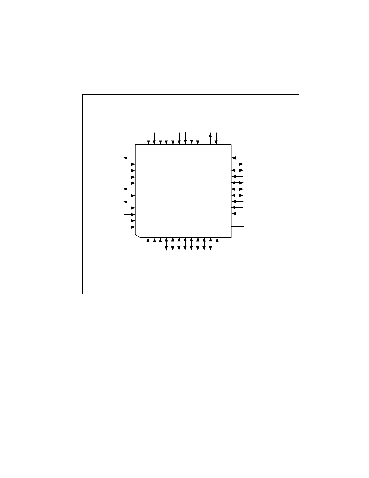
PIN CONFIGURATION
VCOREA
VINR0
+3.3VIN
+5VIN
+12VIN
-12VIN
VBAT
5VSB
-5VIN
GNDA
BEEP/nGPO
VID3
VREF
VTIN3/PIITD3
VTIN2PIITD2
VTIN1PIITD1
VID0
nOVT
ARDMSEL
nSMI
SA2/IA2
SA1/IA1
SA0/IA0
nCS
3635343332313029282726
37
38
39
40
41
42
MON35W42
43
44
45
46
47
48
1234567891011
nIOR
D7D6D5D4D3
nIOW
CLKIN
D2
25
24
23
22
21
20
19
18
17
16
15
14
13
12
VID1
D1/PWMOUT4
D0/PWMOUT3
VID2
PWMTOUT1
SDA
SCL
FAN1IO
FAN2IO
FAN3I0/PWMOUT2
VID4
CASEOPEN
MR
GNDD
VCC
5
Page 6

PIN DESCRIPTION
I/O
- TTL level bi-directional pin with 12 mA source-sink capability
12t
I/O
- TTL level and schmitt trigger
12ts
OUT
- Output pin with 12 mA source-sink capability
12
AOUT - Output pin (Analog)
OD
- Open-drain output pin with 12 mA sink capability
12
IN
- TTL level input pin
t
IN
- TTL level input pin and schmitt trigger
ts
AIN - Input pin (Analog)
DESCRIPTION OF PIN FUNCTIONS
PIN NAME PIN NO. TYPE DESCRIPTION
nIOR 1 INts An active low standard ISA bus I/O Read
Control.
nIOW 2 INts An active low standard ISA bus I/O Write
Control.
CLKIN 3 INt System clock input. Can select 48MHz or 24MHz
or 14.318MHz. The default is 24MHz.
D7~D2 4-9 I/O
D1/
10 I/O
PWMOUT4
D0/
11 I/O
PWMOUT3
VID1 12 INt Voltage Supply readouts from P6. This value is
VCC (+5V) 13 POWER +5V VCC power. Bypass with the parallel
GNDD 14 DGROUND Internally connected to all digital circuitry.
MR 15 INts Master reset input.
nCASEOPEN 16 INt CASE OPEN detection. An active low input from
VID4 17 INt Voltage Supply readouts from P6. This value is
FAN3IO/
18 I/O
PWMOUT2
Bi-directional ISA bus Data lines. D0
12t
corresponds to the low order bit, with D7 the
high order bit. These pins are activated if pin
ADRMSEL=0.
Bi-directional ISA bus Data lines. This pin is
activated if pin ADRMSEL=0. /Fan speed control
PWM output. This pin is activated if pin
ADRMSEL=1.
Bi-directional ISA bus Data lines. This pin is
activated if pin ADRMSEL=0. /Fan speed control
PWM output. This pin is activated if pin
ADRMSEL=1.
OUT
OUT
12t
12t
12t
12t
read in the VID/Fan Divisor Register.
combination of 10&F (electrolytic or tantalum)
and 0.1&F (ceramic) bypass capacitors.
an external device when the case is opened.
This signal can be latched if VBAT is connect to
a battery, even if the MON35W42 is power off.
read in the bit <0> of Device ID Register.
0V to +5V amplitude fan tachometer input. /
12t
Fan speed control PWM output.
6
Page 7

PIN NAME PIN NO. TYPE DESCRIPTION
FAN2IO-FAN1IO
19-20 I/O
0V to +5V amplitude fan tachometer input /
12t
Fan on-off control output. These multi-functional
pins can be programmable input or output.
SCL 21 INts Serial Bus Clock.
SDA 22 I/O
PWMOUT1 23 OUT
Serial Bus bi-directional Data.
12ts
Fan speed control PWM output.
12t
VID2 24 INt Voltage Supply readouts from P6. This value is
read in the VID/Fan Divisor Register.
VID3 25 INt Voltage Supply readouts from P6. This value is
read in the VID/Fan Divisor Register.
BEEP/nGPO 26 OD48 Beep (Default) / General purpose output
This multi-functional pin is programmable.
GNDA 27 AGROUND Internally connected to all analog circuitry. The
ground reference for all analog inputs.
-5VIN 28 AIN 0V to 4.096V FSR Analog Inputs.
5VSB 29 AIN 0V to 4.096V FSR Analog Inputs.
VBAT 30 AIN 0V to 4.096V FSR Analog Inputs. (This pin
should be connected to a 3V BATTERY.)
-12VIN 31 AIN 0V to 4.096V FSR Analog Inputs.
+12VIN 32 AIN 0V to 4.096V FSR Analog Inputs.
+5VIN 33 AIN This pin is Analog Vcc and connects internal
monitor channel IN3 with fixed scale.
+3.3VIN 34 AIN 0V to 4.096V FSR Analog Inputs.
VINR0 35 AIN 0V to 4.096V FSR Analog Inputs.
VCOREA 36 AIN 0V to 4.096V FSR Analog Inputs.
VREF 37 AOUT Reference Voltage.
VTIN3 /
PIITD3
38 AIN Thermistor 3 terminal input.(Default) /
Pentium
®
II diode 3 input.
This multi-functional pin is programmable.
VTIN2 /
PIITD2
39 AIN Thermistor 2 terminal input. (Default)/
Pentium
®
II diode 2 input.
This multi-functional pin is programmable.
VTIN1 /
PIITD1
40 AIN Thermistor 1 terminal input. (Default)/
Pentium
®
II diode 1 input.
This multi-functional pin is programmable.
VID0 41 INt Voltage Supply readouts from P6. This value is
read in the VID/Fan Divisor Register.
nOVT 42 OD
Over temperature Shutdown Output.
12t
ADRMSEL 43 INt Pin 45--47 mode selection.
0 = The 3 lowest order bits of ISA Address
Bus.(Default, internal pull-down 47K ohm)
1 = 7 bit I
2
C address setting pin.(bit2 - bit0)
7
Page 8

PIN NAME PIN NO. TYPE DESCRIPTION
nSMI 44 OD12 System Management Interrupt (open drain). This
output is enabled when Bit 1 in the Configuration
Register is set to 1. The default state is disabled.
SA2-SA0
IA2,IA1,IA0
45-47 IN
IN
t
t
The three lowest order bits of the 16-bit ISA
Address Bus. A0 corresponds to the lowest
order bit.
(Default, when ARDMSEL =0 or left open )
The hardware setting pin of 7 bit I2C serial
address bit2, bit1 and bit0. (When ARDMSEL
=1)
nCS 48 INt Chip Select input from an external decoder,
which decodes high order address bits on the
ISA Address Bus. This is an active low input.
8
Page 9

FUNCTIONAL DESCRIPTION
General Description
The MON35W42 provides 7 analog positive
inputs, 3 fan speed monitors, up to 4 sets of fan
PWM (Pulse Width Modulation) control, 3
thermal inputs from remote thermistors or
2N3904 transistors or Pentium
thermal diode outputs, case open detection and
beep function output. When the monitored value
exceed the set limit value for voltage,
temperature, or fan counter, the beep output can
be generated. Once the monitor function on the
chip is enabled, the watch dog machine monitors
each function and stores the values. If the
monitored value exceeds the limit value, the
interrupt status is set to 1and an interrupt can be
generated.
®
II (Deschutes)
Access Interface
The MON35W42 provides two interfaces for the
microprocessor to read/write internal registers.
ISA interface
The ISA Bus can be used to access the internal
registers of the MON35W42. This uses an Index
register and Data register to access the internal
registers. The upper address bits of the ISA bus
(bits15:3) must be externally decoded for the
Chip Select (nCS), the recommended address is
290h-297h. The Chip then uses the lower three
ISA address bits (bits 2:0) to decode the Index
and Data Registers. These two I/O registers are
described as following:
Port 295h: Index register.
Port 296h: Data register
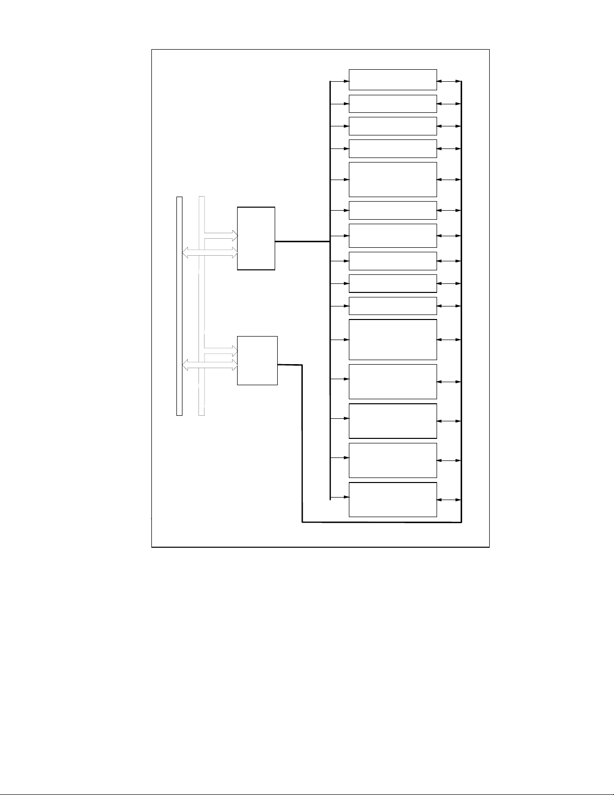
The register structure is shown in Figure 1.
9
Page 10
ISA
ISA
Data
Address
Bus
Bus
Port 5h
Index
Register
Port 6h
Data
Register
2
I
C Interface
The second interface uses the I
FIGURE 1 – ISA INTERFACE ACCESS
2
C Serial Bus.
The MON35W42 uses three serial bus
addresses. The first address defined at CR[48h]
Configuration Register
40h
nSMI Status/Mask Registers
41h, 42h, 44h, 45h
VID<3:0>/Fan Divisor Register
Temperature 2, 3 Serial
Bus Address
Select Bank for 50h~5Fh Reg.
Temperature 2 Control/Staus
Registers
Temperature 3 Control/Staus
Registers
47h
Serial Bus Address
48h
Monitor Value Registers
20h~3Fh
and
60h~7Fh (auto-increment)
VID<4>/Device ID
49h
4Ah
Control Register
4Bh~4Dh
4Eh
Winbond Vendor ID
4Fh
BANK 0
R-T Table Value
BEEP Control Register
Winbond Test Register
50h~58h
BANK 1
50h~56h
BANK 2
50h~56h
can read/write all registers excluding Bank 1 and
Bank 2 temperature sensor 2/3 registers. The
second address defined at CR[4Ah] bit2-0 can
BANK 4
Additional Control/Staus
Registers
50h~5Ch
BANK 5
Additional Limit Value &
Value RAM
50h~57h
only be used to read/write temperature sensor 2
registers, and the third address defined at
10
Page 11
CR[4Ah] bit6-4 can only be used to access
(read/write) temperature sensor 3 registers.
The first serial bus address, CR[48h],
uses 3 hardware setting bits. When pin 43 is set
high, pins 47-45 are used to set the I
for register CR[48h]. The selected address is
00101[pin45][pin46][pin47]. If pin45=1, pin46=1,
pin47=0, the content of CR[48h] is 00101110.
CR[4Ah] is used to set the other two I
addresses. If CR[4Ah] bit 2-0 is XXX , the
temperature sensor 2 serial address is
1001XXXG, in which G is the read/write bit. If
CR[4Ah ] bi t 6- 4 is YYY , the tem per atu re se nso r
3 serial address is 1001YYYG, in wh ich G is the
read/write bit.
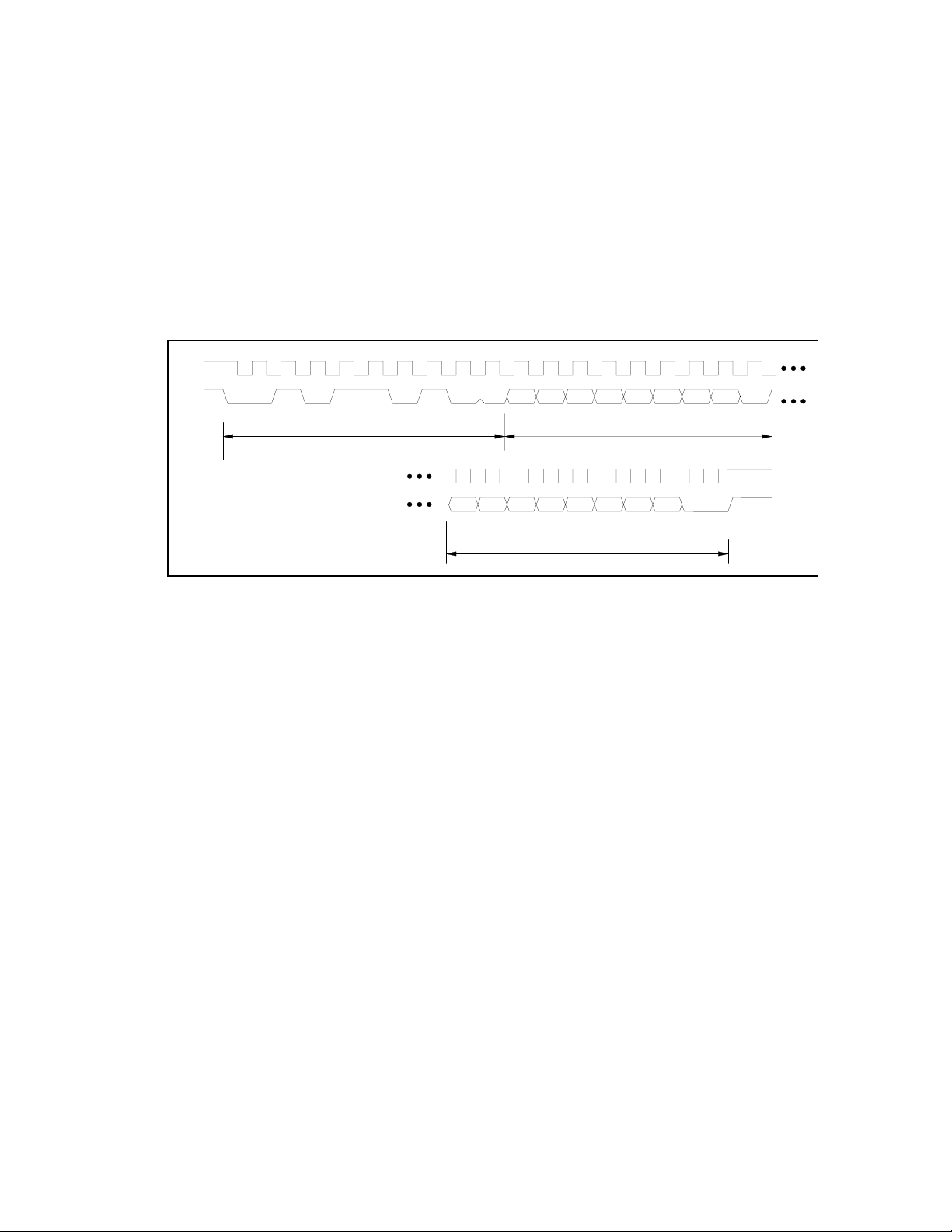
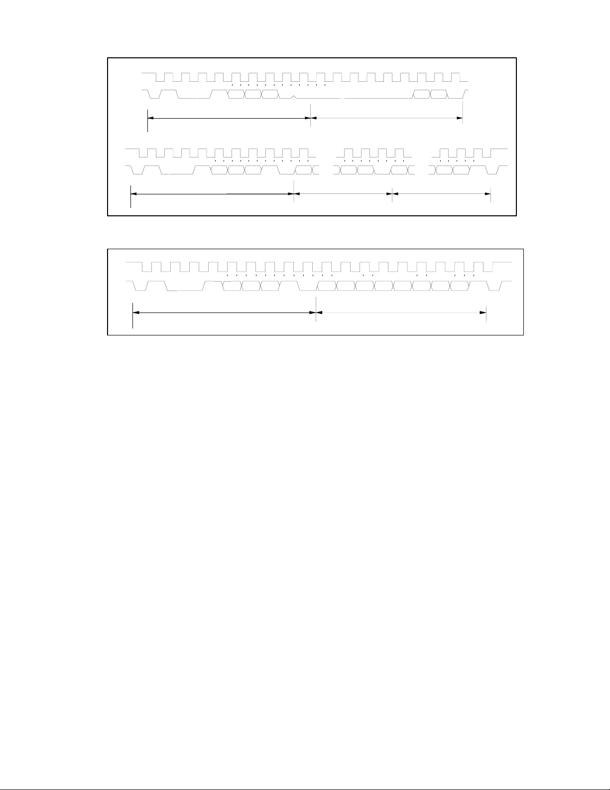
The first serial bus access timing are shown
as follows:
(a)
Serial bus write to internal address register followed by the data byte
SCL
SDA
0
0 1 0 1 1 0 1 D7 D6 D5 D4 D3 D2 D1 D0
Start By
Master
Frame 1
Serial Bus Address Byte
SCL
(Continued)
780 78
R/nW
Ack
by
MON35W42
0
Internal Index Register Byte
SDA (Continued)
D7 D6 D5 D4 D3 D2 D1 D0
Frame 3
Data Byte
FIGURE 2 – SERIAL BUS WRITE TO INTERNAL ADDRESS REGISTER
FOLLOWED BY THE DATA BYTE
Frame 2
78
Ack
by
MON35W42
2
C address
Ack
by
MON35W42
Stop
by
Master
2
C
11
Page 12
(b)
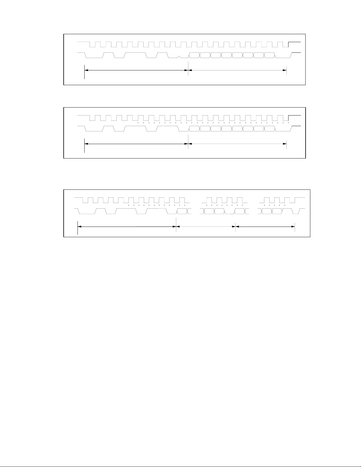
Serial bus write to internal address register only
SCL
SDA
0
0 1 0 1 1 0 1 D7 D6 D5 D4 D3 D2 D1 D0
Start By
Master
Frame 1
Serial Bus Ad dr e ss By te
780 78
R/nW
Ack
MON35W42
0
by
Internal Index Register Byte
Frame 2
MON35W42
FIGURE 3 – SERIAL BUS WRITE TO INTERNAL ADDRESS REGISTER ONLY
(c)
Serial bus read from a register with the internal address register preset to desired location
SCL
0
780 78
SDA
0101101 D7D6D5D4D3D2D1D0
Start By
Master
Frame 1
Serial Bus Address Byte
R/nW
MON35W42
0
Ack
by
Internal Index Register Byte
Frame 2
FIGURE 4 – SERIAL BUS WRITE TO INTERNAL ADDRESS REGISTER
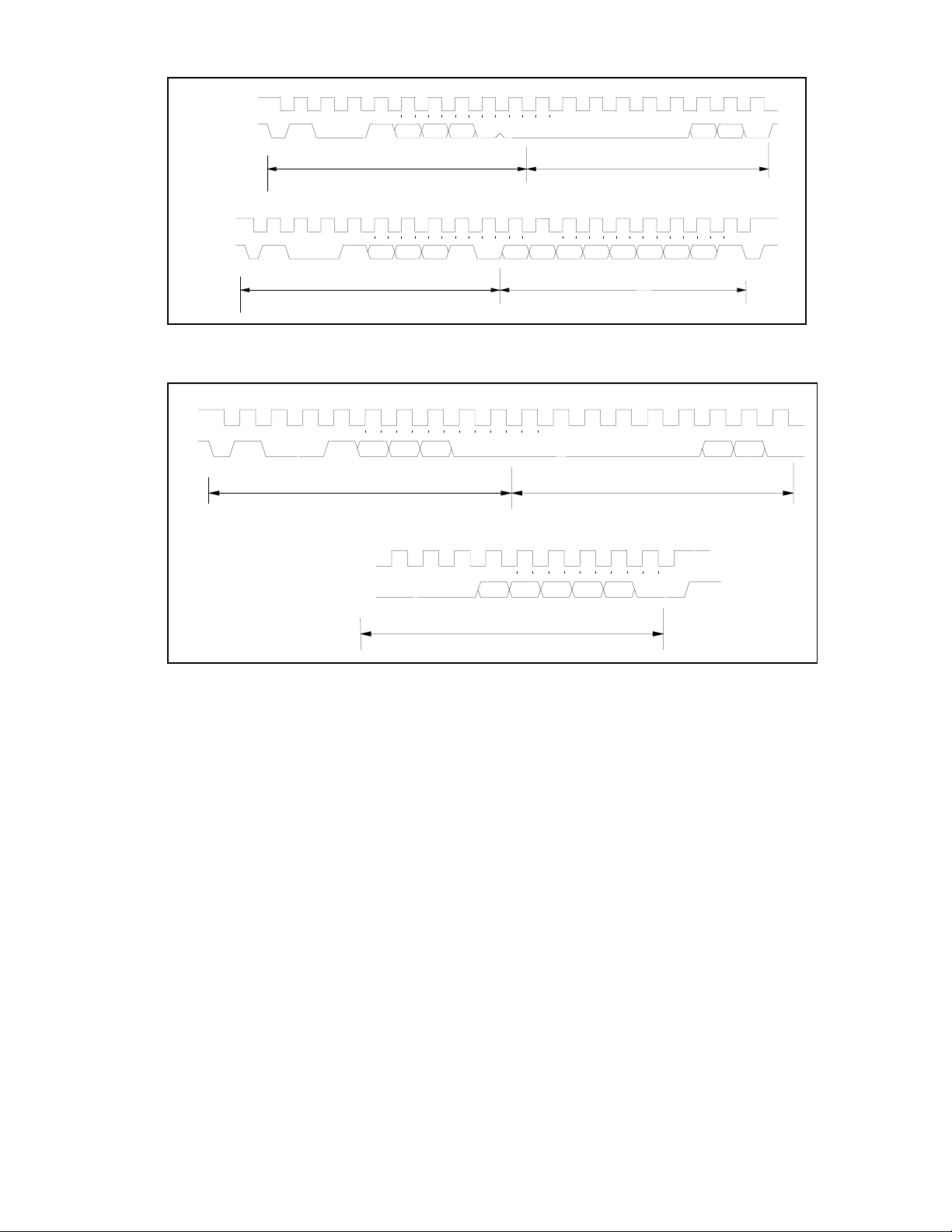
The serial bus timing of the temperature 2 and 3 is shown as follow:
(a) Typical 2-byte read from preset pointer location (Temp, T
OS
, T
HYST
)
SCL
SDA
0
0101101 D7 D1D0
Start By
Master
Frame 1
Serial Bus Address Byte
780 78
R/nW
MON35W42
... ...
...
Ack
by
Frame 2
MSB Data Byte
07
D7 D1 D0
Ack
by
Master
...
LSB Data By te
Frame 3
FIGURE 5 – TYPICAL 2-BYTE READ FROM PRESENT POINTER LOCATION
Ack
by
Ack
by
Master
Ack
by
Master
Stop by
Master
Stop by
Master
Stop by
Master
12
Page 13
Typical pointer set followed by immediate read for 2-byte register (Temp, TOS, T
(b)
HYST
)
SCL
SDA
0
1001A2A1A0
Start By
Master
Frame 1
Serial Bus Address Byte
780
MON35W42
Ack
by
R/nW
000000
Frame 2
Pointer Byte
4
D1 D0
MON35W42
Ack
by
... ...
...
D7 D1 D0
Ack
by
Frame 4
MSB Data Byte
07
...
D7 D1 D0
Ack
by
Master
Frame 5
LSB Data Byte
No Ack
by
Master
Stop by
Master
SCL
SDA
0
1001A2A1A0
Start By
Master
Frame 3
Serial Bus Address Byte
780 78
R/nW
MON35W42
0
FIGURE 6 – TYPICAL POINTER SET FOLLOWED BY IMMEDIATE READ FOR 2-BYTE REGISTER
(c)
Typical read 1-byte from configuration register with preset pointer
SCL
SDA
0
1001
Start By
Master
A2 A1 A0
Frame 1
Serial Bus Addr ess Byte
780
R/nW
MON35W42
D7 D2
Ack
by
Frame 2
Data Byte
7
8
D0
D1D5 D4 D3D6
No Ack
by
Master
Stop by
Master
FIGURE 7 – TYPICAL 1-BYTE READ FROM CONFIGURATION WITH RESET
13
Page 14
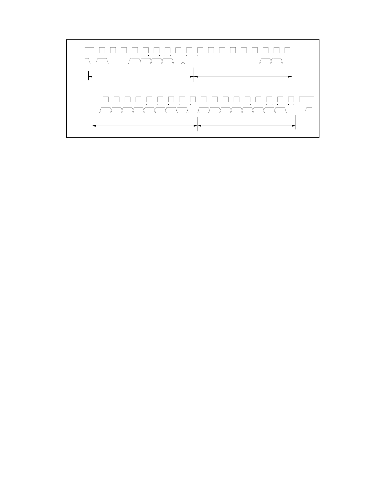
(d) Typical pointer set followed by immediate read from configuration register
780
R/nW
Ack
by
MON35W42
4
000000
Frame 2
Pointer Byte
D1 D0
SCL
SDA
0
1001A2A1A0
Start By
Master
Frame 1
Serial Bus Address Byte
SCL (Cont..)
SDA (Cont..)
0
1001
Repea
Start
By Master
A2 A1 A0
Frame 3
Serial Bus Address Byte
780
MON35W42
Ack
by
D7 D5 D4
R/nW
D6 D3
Frame 4
MSB Data Byte
7
D2 D1 D0
FIGURE 8 – TYPICAL POINTER SET FOLLOWED BY IMMEDIATE READ FROM TEMP 2/3
CONFIGURATION REGISTER
(e) Temperature 2/3 configuration register Write
4
SCL
0
780
R/nW
SDA
1 0 0 1 A2 A1 A0
Start By
Master
Frame 1
Serial Bus Address Byte
0000000
Ack
MON35W42
by
Frame 2
Pointer Byte
0
SCL (Cont...)
SDA (Cont...)
0 0 D4 D 3 D2 D10D0
FIGURE 9 – CONFIGURATION REGISTER WRITE
Frame 3
Configuration Data Byte
78
Ack
by
MON35W42
Stop
by
Master
78
MON35W42
8
No Ack
by
Master
D1 D0
...
...
Ack
by
Stop by
Master
78
Ack
by
MON35W42
14
Page 15
(f)
Temperature 2/3 TOS and T
SCL
SDA
SCL (Cont...)
SDA (Cont...)
0
1001A2A1A0
Start By
Master
0
D6 D5 D4 D3 D2 D1D7 D0
write
HYST
780
0
0
0000
Frame 2
Pointer Byte
Frame 1
Serial Bus Address Byte
R/nW
Ack
by
78
0
D6 D5 D4 D3 D2 D1D7 D0
Frame 4
LSB Data Byte
Frame 3
MSB Data Byte
MON35W42
Ack
by
FIGURE 10 – CONFIGURATION REGISTER WRITE
D1 D0
78
Ack
by
MON35W42MON35W42
78
Ack
by
MON35W42
Stop
Master
by
4
15
Page 16

Analog Inputs
The maximum input voltage of the analog pin is
4.096V, the 8-bit ADC has a 16mv LSB. For
most PC applications, the analog inputs are
connected to the power suppliers. The CPU V-
Positive Inputs
R1
V1
Positive Input
Negative Input
Typical Thermister Connection
V3
V4
R7
R2
R
10K, 25 C
THM
FIGURE 11
core voltage,+3.3V and battery voltage can
directly connected to these analog inputs. The
5VSB and +12V inputs should be reduced using
external resistors to obtain the proper input
range. Refer to Figure 11.
12VIN
V2
+2.5VINA
+2.5VINB
+3.3VIN
VDD(+5V)
VBAT
R3
R4
Pin 36
Pin 35
Pin 34
Pin 33
Pin 30
Pin 32
5VSB Pin 29
8-bit ADC
with
16mV LSB
R5
N12VIN
N5VIN
Pin 31
Pin 28
R
10K, 1%
R8
VREF Pin 37
VTIN3
VTIN2
VTIN1
Pin 38
Pin 39
Pin 40
R6
**The Connections of VTIN1 and VTIN2
are same as VTIN3
16
Page 17

Monitor over 4.096V voltage:
The input voltage +12VIN can be expressed using the following equation.
R
2
12
VINV
'(
1
RR
12
The value of R1 and R2 can be selected as 28K Ohms and 10K Ohms, respectively, when the input
voltage V1 is 12V. The node voltage of +12VIN will be subject to less than 4.096V for the maximum
input range of the 8-bit ADC. Similarly, the node voltage of 5VSB (measured standby power VSB for
ATX power supply) also can be monitored by using two series resistors R3 and R4 which can be 5.1K
ohms and 7.5K ohms so as to obtain the 5VSB as lim ited to less than 4.096V. Pin 33 is connected to
the power supply VCC at +5V. This pin supports two functions. The first function is to supply internal
analog power in the MON35W42 and the second function is to monitor the 5V input through internal
series resistors. The values of the two series resistors are 34K ohms and 50K ohms so that input
voltage to ADC is 2.98V which is less than 4.096V of the ADC maximum input voltage. The voltage
equation can be represent as follows.
K
50
VVCC
'(
in
Monitor negative voltage:
The negative voltage should be connected to series resistors and a positive voltage VREF (equal to
3.6V). In Figure 11, the voltage V3 and V4 are two negative voltages, -12V and -5V respectively. The
voltage V3 is connected to two series resistors and is then connected to VREF which is a positive
voltage. The voltage at node N12VIN must be a positive voltage and will if the values of the two series
resistors are carefully selected. If the value of two series resistors are R5=232K ohms and R6=56K
ohm. The input voltage of node N12VIN can be calculated by the following equation.
NVIN VREF V
If V
is equal to -12V then the voltage is equal to 0.567V and the converted hexdecimal data is set to
5
35h by the 8-bit ADC with 16mV-LSB. This monitored value should be converted to the real negative
voltage and the voltage is calculated by the following equation.
Where
-
is 232K/(232K+56K). If the N2VIN is 0.567 then the V5 is approximately equal to -12V.
')(
V
5
50 34
where VCC is set to 5V.
where VREF is equal 3.6V.
NVIN VREF
12
'
+
KK
)
++
55
232 56
,(
-
1
,
)
298
K
)
-
+
V
.
*
232
KK
++
V12
)()( )
17
Page 18

The other negative voltage input V6 (approximate -5V) also can be evaluated by a similar method and
the series resistors can be selected as R7=120K ohms and R8=56K ohms. The equation for a V6 of 5V voltage is as follows.
NVIN VREF
5
V
'
6
Where
VREF=3.6V and the parameter . is 0.6818 then the negative voltage of V6 can be -5V.
Monitor temperature from thermistor:
The MON35W42 can connect to three thermistors to measure three different environment
temperatures. The specification of thermistor is: (1) - value is 3435K, (2) resistor value is 10K ohms at
25%C. In Figure 11, the themistor is connected by a series resistor to a 10K Ohms resistor, then to
VREF (Pin 37).
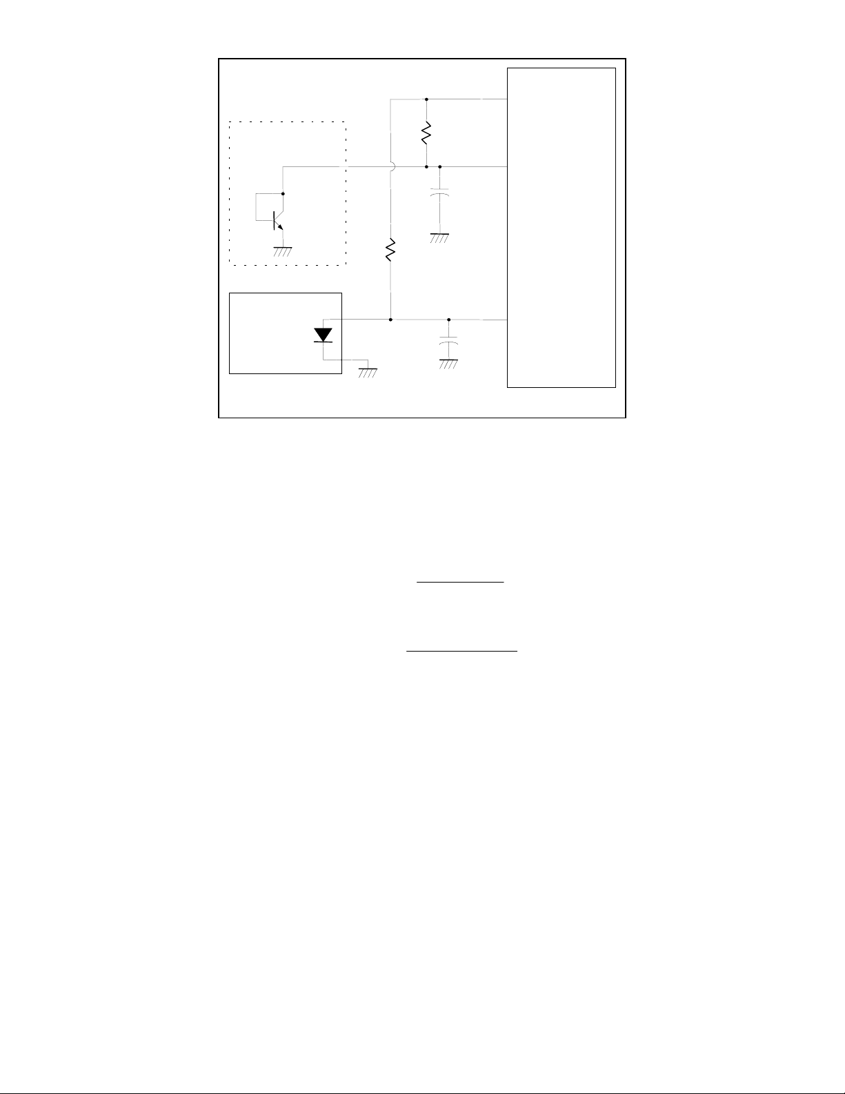
Monitor temperature from Pentium
The MON35W42 can monitor the temperature from the Pentium
or a 2N3904 transistor. The circuit is shown in Figure 12. The Pentium
supply ground (GND) and the D+ pin is connected to pin PIITDx in the MON35W42. The resistor
R=30K ohms is connected to VREF to supply the diode bias current and the bypass capacitor
C=3300pF is used to filter the high frequency noise. The transistor 2N3904 is to a form a diode, the
Base (B) and Collector (C) in the 2N3904 are tied together to act as a thermal diode.
.
is 120K/(120K+56K). If the monitored ADC value in the N5VIN channel is 0.8635,
®
II thermal diode or bipolar transistor 2N3904
,(
.
1
,
.
®
II (Deschutes) thermal diode interface
®
II D- pin is connected to power
18
Page 19
r
Bipolar Transistor
Temperature Sens or
R=30K, 1%
VREF
PIITDx
C
B
2N3904
E
OR
Pentium II
CPU
Therminal
Diode
R=30K, 1%
D+
D-
C=3300pF
MON35W82
PIITDx
C=3300pF
FIGURE 12
FAN Speed Count and FAN Speed Control
Fan speed count
Fan speed count inputs provide for signals from fans equipped with tachometer outputs. These signals
must be TTL level, and the maximum input voltage can not be over Vcc. If the input signals from the
tachometer outputs are above VCC, the external voltage must be reduced using external components
to obtain the proper input voltage. The normal circuit and trimming circuits are shown in Figure 13.
Determine the fan counter according to:
Count
.
'
(
RPM Divisor
6
(
135 10
In other words, once the fan speed counter has been read from register CR28 or CR29 or CR2A, the
fan speed can be evaluated by the following equation.
RPM
'
.
Count D ivi so
(
6
(
135 10
The default divisor is 2 and defined in CR47.bit7~4, CR4B.bit7~6, and Bank0 CR5D.bit5~7 which
contain the three bits for the divisor. This provides very low speed fan counter support for fans such as
power supply fan. The followed table is an example for the relation of divisor, RPM, and count.
19
Page 20
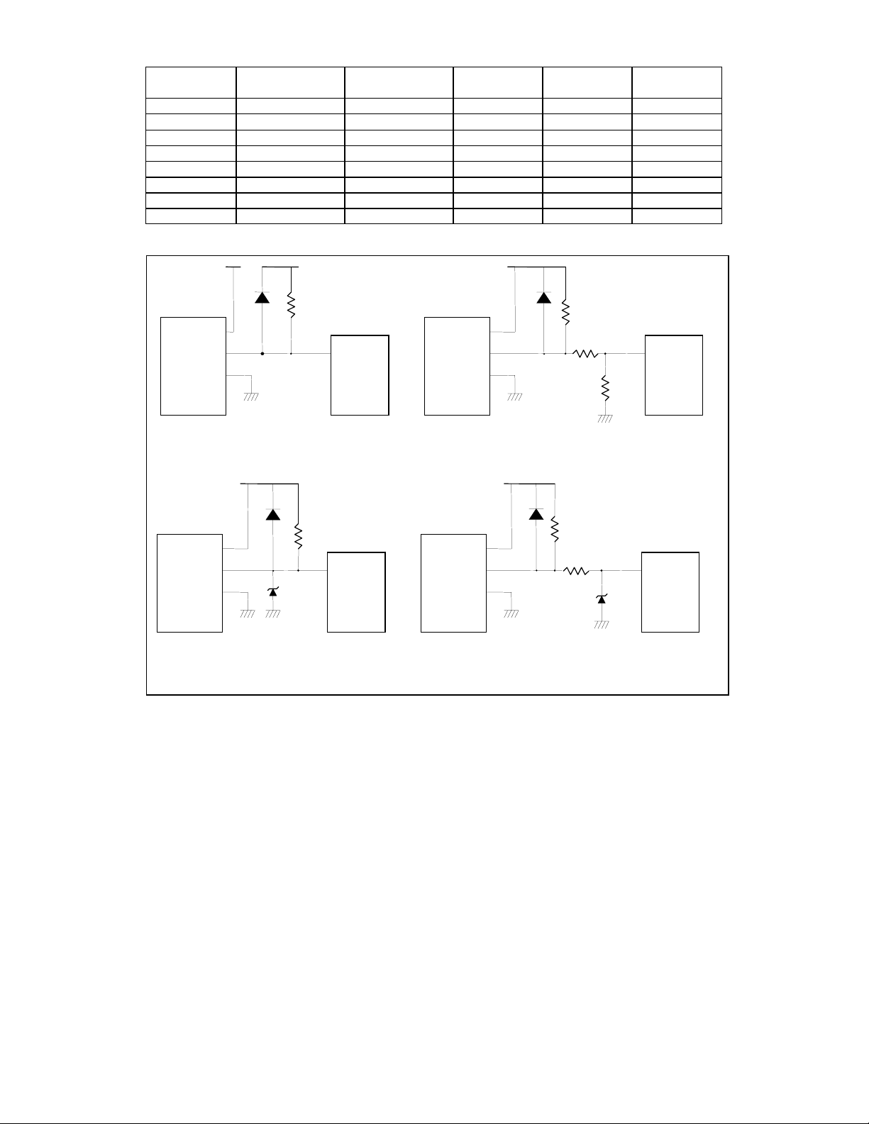
Table 1
DIVISOR
NOMINAL
RPM
TIME PER
REVOLUTION COUNTS
1 8800 6.82 ms
2 (default)
4400 13.64 ms
4 2200 27.27 ms
8 1100 54.54 ms
16 550 109.08 ms
32 275 218.16 ms
64 137 436.32 ms
128 68 872.64 ms
Connector
diode diode
+12V
FAN Out
GND
FAN
+5V+12V
Pull-up resister
4.7K Ohms
Fan Input
Pin 18/19/20
MON35W82
Connector
FAN Out
FAN
+12V
GND
153
153
153
153
153
153
153
153
+12V
70% RPM
TIME FOR
70%
6160 9.74 ms
3080 19.48 ms
1540 38.96 ms
770 77.92 ms
385 155.84 ms
192 311.68 ms
96 623.36 ms
48 1246.72 ms
Pull-up resister
4.7K Ohms
14K~39K
Fan Input
10K
Pin 18/19/20
MON35W82
Figure 13A - Fan with Tach Pull-Up to
+5V
+12V
FAN Out
FAN
Connector
diode
+12V
GND
Pull-up resister
Fan Input
3.9V Zener
> 1K
Pin 18/19/20
MON35W82
Figure 13C - Fan with Tach Pull-Up to
+12V and
Zener Clamp
Figure 13B - Fan with Tach Pull-U p to +12V, or
Totem-Pole
FAN Out
FAN
Connector
Output and Register Attenuator
+12V
3.9V
> 1K
Zener
Pull-up resister < 1K
or totem-pole output
diode
+12V
GND
Fan Input
Pin 18/19/20
MON35W82
Figure 13D - Fan with Tach Pull-Up to +12V, or
Totem-Pole Putpu t and Zener Clam p
20
Page 21
Fan speed control
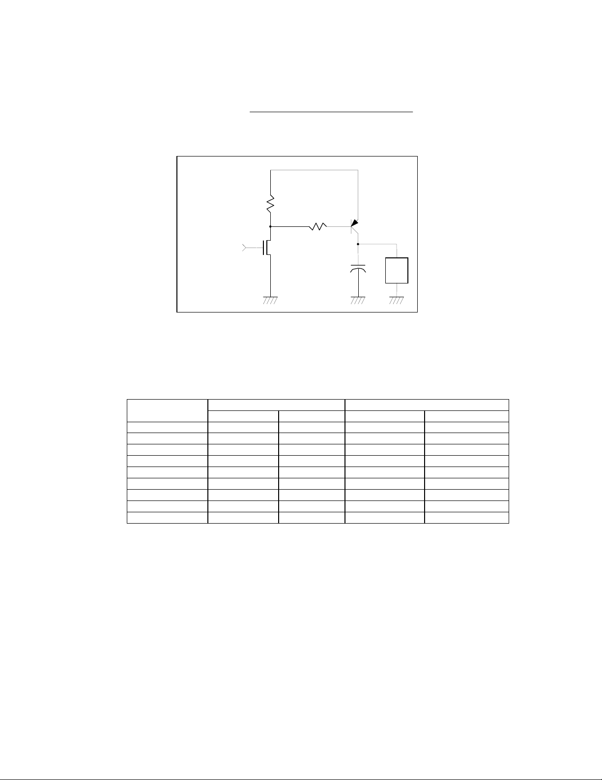
The MON35W42 provides four sets of controls for fan PWM speed control. The duty cycle of the PWM
can be programmed by a 8-bit registers which are defined in the Bank0 CR5A, CR5B, CR5E, and
CR5F. The default duty cycle is set to 100%, the default 8-bit registers is set to FFh. The duty cycle can
be calculated as follows.
(%)cycleDuty
ValueRegister bit -8 Programmed
%100
('
255
The PWM clock frequency also can be program and defined in the Bank0.CR5C and Bank4.CR5C.
The application circuit is shown in figure 14.
+12V
R1
D
PWM Clock Input
G
NMOS
S
Temperature Measurement Machine
The temperature data format is 8-bit two’s-complement for sensor 1 and 9-bit two’s-complement for
sensors 2/3. The 8-bit temperature data can be obtained by reading the CR[27h]. The 9-bit temperature
data can be obtained by reading the 8 MSBs from the Bank1/2 CR[50h] and the LSB from the Bank1/2
CR[51h] bit 7. The format of the temperature data is show in Table 1.
8-Bit Digital Output 9-Bit Digital Output
Temperature
8-Bit Binary 8-Bit Hex 9-Bit Binary 9-Bit Hex
+125°C 0111,1101 7Dh 0,1111,1010 0FAh
+25°C 0001,1001 19h 0,0011,0010 032h
+1°C 0000,0001 01h 0,0000,0010 002h
+0.5°C - - 0,0000,0001 001h
+0°C 0000,0000 00h 0,0000,0000 000h
-0.5°C - - 1,1111,1111 1FFh
-1°C 1111,1111 FFh 1,1111,1110 1FFh
-25°C 1110,0111 E7h 1,1100,1110 1CEh
-55°C 1100,1001 C9h 1,1001,0010 192h
R2
FIGURE 14
Table 2
PNP Transistor
+
C
-
FAN
21
Page 22
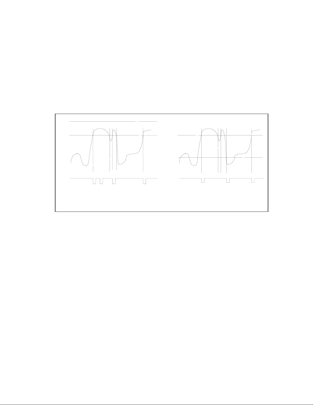
Temperature sensor 1 nSMI interrupt modes:
(1) Comparator Interrupt Mode
Setting the T
(Temperature Hysteresis) limit to 127°C will set temperature sensor 1 nSMI to the
HYST
Comparator Interrupt Mode. Temperatures which exceed TO (Over Temperature) Limit cause an
interrupt. This interrupt is reset by reading the Interrupt Status Register. Once an interrupt event has
occurred by exceeding T
, and then reset, if the temperature remains above the TO, the interrupt will
O
occur again when the next conversion has completed. If an interrupt event has occurred by exceeding
T
and is not reset, the interrupts will not occur again. The interrupts will continue to occur in this
O
manner until the temperature goes below T
. (Figure 16-1)
O
(2) Two-Times Interrupt Mode
Setting the T
The Temperature exceeding T
lower than TO will set temperature sensor 1 nSMI to the Two-Times Interrupt Mode.
HYST
causes an interrupt and then the temperature going below T
O
HYST
also
causes an interrupt if the previous interrupt has been reset by reading the interrupt Status Register.
Once an interrupt event has occurred by exceeding T
the T
, additional interrupts will not occur. (Figure 15-2)
HYST
, then reset, if the temperature remains above
O
T
HYST
127'C
T
OI
nSMI
FIGURE 15-1 - COMPARATOR INTERRUPT MODE
*
*
*
*Interrupt Reset when Interrupt St atus Register s are read
T
OI
T
HYST
nSMI
*
*
*
*
FIGURE 15-2 - TWO-TIMES INTERRUPT MODE
22
Page 23
Temperature sensor 2 and sensor 3 nSMI interrupt
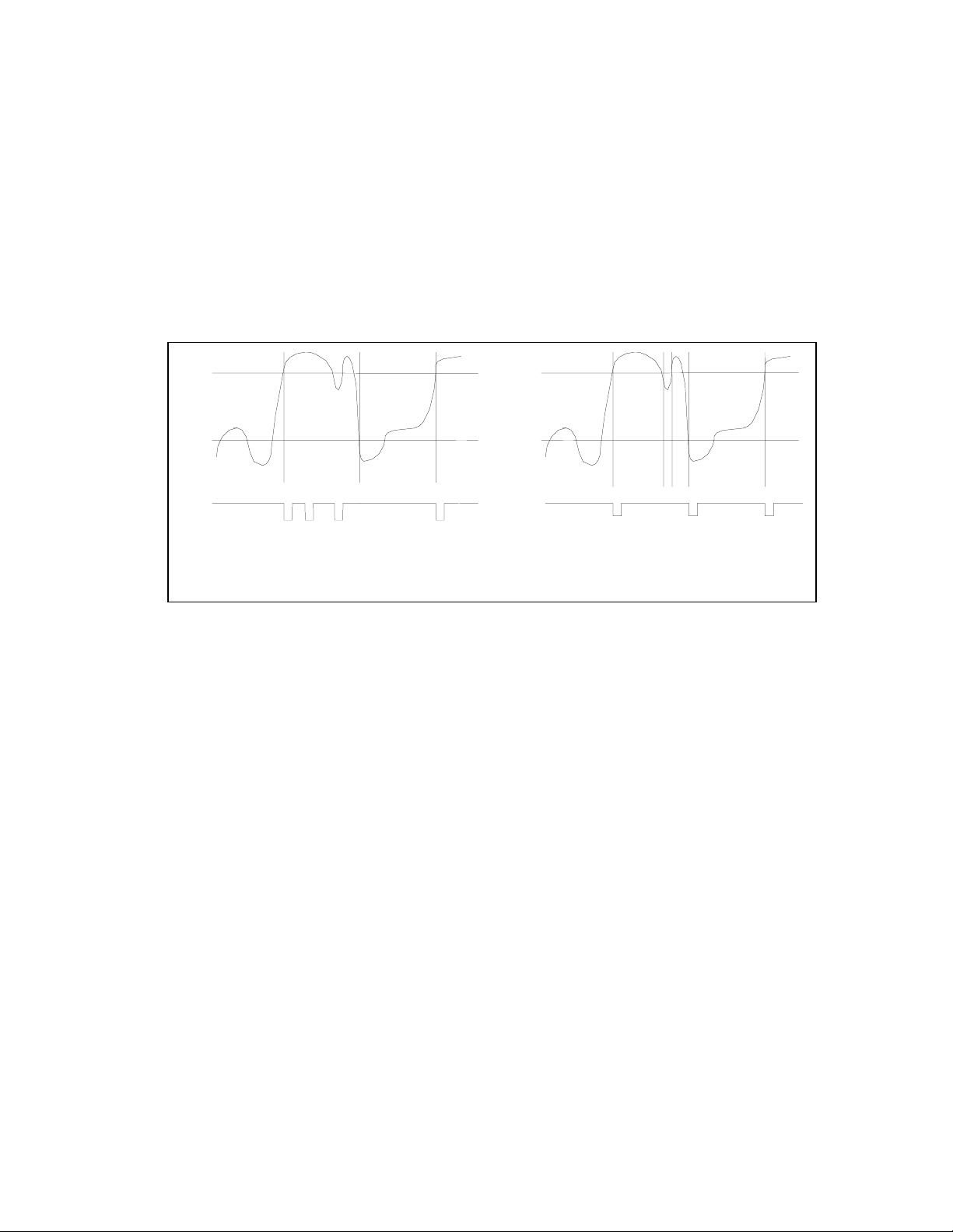
Temperature sensor 2 and sensor 3 nSMI interrupt have two modes of operation and are programmed
at CR[4Ch] bit 6.
(1) Comparator Interrupt Mode
Temperatures exceeding T
Register. Once an interrupt event has occurred by exceeding T
remains above the T
interrupt event has occurred by exceeding T
interrupt continues to occur in this manner until the temperature goes below T
cause an interrupt. This interrupt is reset by reading the Interrupt Status
O
, the interrupt occurs again when the next conversion has completed. If an
HYST
and is not reset, the interrupt will not occur again. The
O
, and then reset, if the temperature
O
. (Figure 16-1)
HYST
(2) Two-Times Interrupt Mode
Temperatures exceeding T
cause an interrupt and then when the temperature going below T
O
HYST
it will
also cause an interrupt if the previous interrupt has been reset by reading the interrupt Status Register.
Once an interrupt event has occurred by exceeding T
above the T
, the interrupt will not re-occur. (Figure 16-2)
HYST
, and then reset, if the temperature remains
O
T
OI
T
OI
T
HYST
nSMI
FIGURE 16-1 - COMPARATOR INTERRUPT MODE FIGURE 16-2 - TWO-TIMES INTERRUPT MODE
*
*
*
*
*Interrupt Reset when Interrupt St atus Register s are read
*
T
HYST
nSMI
*
*
23
*
Page 24
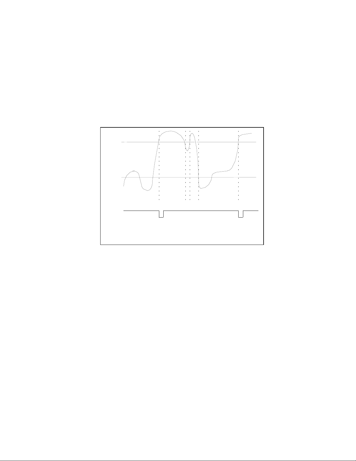
Temperature sensors 2 and 3 Over-Temperature (nOVT)
Temperature sensors 2 and 3 Over-Temparature (nOVT) have two modes of operation. They are
programmed at Bank1 and Bank2 CR[52h] bit1 . These two bits needs to be programmed to the same
value.
(1) Comparator Mode :
Temperatures exceeding T
T
. (Figure 17)
HYST
cause the nOVT output to go active until the temperature is less than
O
(2) Interrupt Mode:
Temperatures exceeding T
temperature sensor 2 or sensor 3 registers. If the temperature exceeds T
and then the temperature going below T
temperature sensor2 or sensor 3 registers. Once the nOVT is activated by exceeding T
the temperature remains above T
causes the nOVT output to go active indefinitely until reset by reading
O
causes the nOVT to go active until reset by reading
HYST
, the nOVT is not be activated again. (Figure 17).
HYST
, and then nOVT is reset,
O
, then reset, if
O
T
OI
T
HYST
nSMI
**
*Interrupt Reset when Interrupt Status Registers are read
FIGURE 17 – OVER TEMPERATURE RESPONSE DIAGRAM
24
Page 25
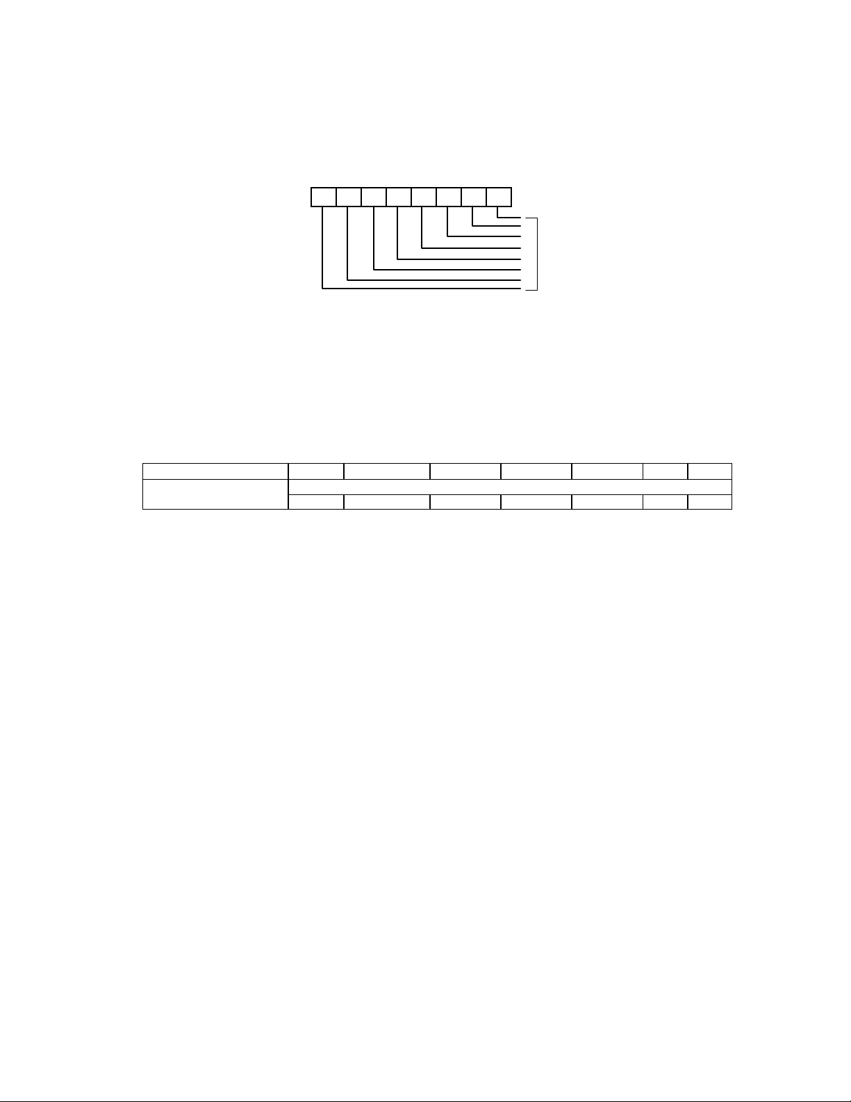
REGISTERS AND RAM
Address Register (Port x5h)
Data Port: Port x5h
Power on Default Value 00h
Attribute: Bit 6:0 Read/write , Bit 7: Read Only
Size: 8 bits
7 6 5 4 3 2 1 0
Data
Bit7: Read Only
The logical 1 indicates the device is busy due to a Serial Bus transaction or another ISA bus
transaction. By checking this bit, multiple ISA drivers can use the MON35W42 without interfering with
each other or a Serial Bus driver. It is the user's responsibility not to have a Serial Bus and ISA bus
operations at the same time.
This bit is:
Set:
with a write to Port x5h or when a Serial Bus transaction is in progress.
Reset:
with a write or read from Port x6h if it is set by a write to Port x5h, or when the Serial Bus
transaction is finished.
Bit 6-0: Read/Write
Bit 7 Bit 6 Bit 5 Bit 4 Bit 3 Bit 2 Bit 1 Bit 0
Busy Address Pointer (Power On default 00h)
(Power On default 0) A6 A5 A4 A3 A2 A1 A0
25
Page 26
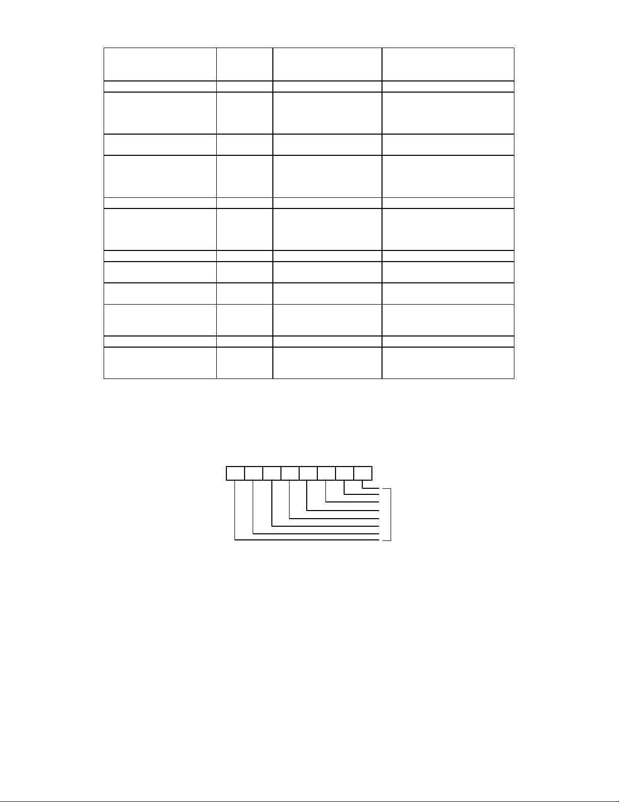
Address Pointer Index (A6-A0)
REGISTERS AND RAM
A6-A0 IN
HEX
POWER ON VALUE
OF REGISTERS:
<k7:0>IN BINARY
NOTES
Configuration Register 40h 00001000
Interrupt Status Register
1
41h 00000000 Auto-increment to the
address of Interrupt Status
Register 2 after a read or
write to Port x6h.
Interrupt Status Register
42h 00000000
2
nSMIÝ Mask Register 1 43h 00000000 Auto-increment to the
address of SMIÝ Mask
Register 2 after a read or
write to Port x6h.
SMIÝ Mask Register 2 44h 00000000
NMI Mask Register 1 45h 00000000 Auto-increment to the
address of NMI Mask
Register 2 after a read or
write to Port x6h
NMI Mask Register 2 46h 01000000
VID/Fan Divisor Register 47h <7:4> = 0101;
<3:0> = VID3-ID0
Serial Bus Address
48h <6:0> = 0101101; <7> = 0
Register
POST RAM 00-1Fh Auto-increment to the next
location after a read or write
to Port x6h and stop at 1Fh.
Value RAM 20-3Fh
Value RAM 60-7Fh Auto-increment to the next
location after a read or write
to Port x6h and stop at 7Fh.
Data Register (Port x6h)
Data Port: Port x6h
Power on Default Value 00h
Attribute: Read/write
Size: 8 bits
7 6 5 4 3 2 1 0
Bit 7-0: Data to be read from or to be written to RAM and Register.
26
Data
Page 27

Configuration Register
Register Location: 40h
Power on Default Value 00000001 binary
Attribute: Read/write
Size: 8 bits
Bit 7: A one restores power-on default values to all registers except the Serial Bus Address register.
This bit clears itself since the power on default is zero.
Bit 6: A logical 1 in this bit drives a zero on BEEP/nGPO pin.
Bit 5: Reserved
Bit 4: Reserved
Bit 3: A one disables the nSMI output without affecting the contents of Interrupt Status Registers. The
device will stop monitoring. It will resume monitoring upon the clearing of this bit.
Bit 2: Reserved
Bit 1: A one enables the nSMI Interrupt output.
Bit 0: A one enables startup of monitoring operations, a zero puts the part in standby mode.
Note:
The outputs of Interrupt pins will not be cleared if the user writes a zero to this location after an
interrupt has occurred unlike "INT_Clear'' bit.
Index 40h
!!!!
7 6 5 4 3 2 1 0
START
nSMIEnable
RESERVED
INT_Clear
RESERVED
RESERVED
BEEP/nGPO
INITIALIZATION
27
Page 28
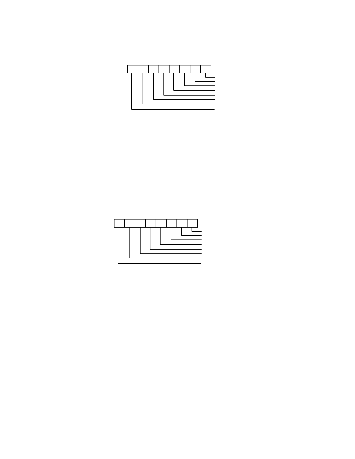
Interrupt Status Register 1
Index 41h
!!!!
Register Location: 41h
Power on Default Value 00h
Attribute: Read Only
Size: 8 bits
7 6 5 4 3 2 1 0
VCOREA
VINRO
+3.3VIN
+5VIN
TEMP1
TEMP2
FAN1
FAN2
Bit 7: A one indicates the fan count limit of FAN2 has been exceeded.
Bit 6: A one indicates the fan count limit of FAN1 has been exceeded.
Bit 5: A one indicates a High limit of VTIN2 has been exceeded from temperature sensor 2.
Bit 4: A one indicates a High limit of VTIN1 has been exceeded from temperature sensor 1.
Bit 3: A one indicates a High or Low limit of +5VIN has been exceeded.
Bit 2: A one indicates a High or Low limit of +3.3VIN has been exceeded.
Bit 1: A one indicates a High or Low limit of VINR0 has been exceeded.
Bit 0: A one indicates a High or Low limit of VCOREA has been exceeded.
Interrupt Status Register 2
Index 42h
!!!!
Register Location: 42h
Power on Default Value 00h
Attribute: Read Only
Size: 8 bits
7 6 5 4 3 2 1 0
+12VIN
-12VIN
-5VIN
FAN3
Chassis Intrusion
Temp3
Reserved
Reserved
Bit 7-6:Reserved.This bit should be set to 0.
Bit 5: A one indicates a High limit of VTIN3 has been exceeded from temperature sensor 3.
Bit 4: A one indicates Chassis Intrusion has gone high.
Bit 3: A one indicates the fan count limit of FAN3 has been exceeded.
Bit 2: A one indicates a High or Low limit of -5VIN has been exceeded.
Bit 1: A one indicates a High or Low limit of -12VIN has been exceeded.
Bit 0: A one indicates a High or Low limit of +12VIN has been exceeded.
28
Page 29
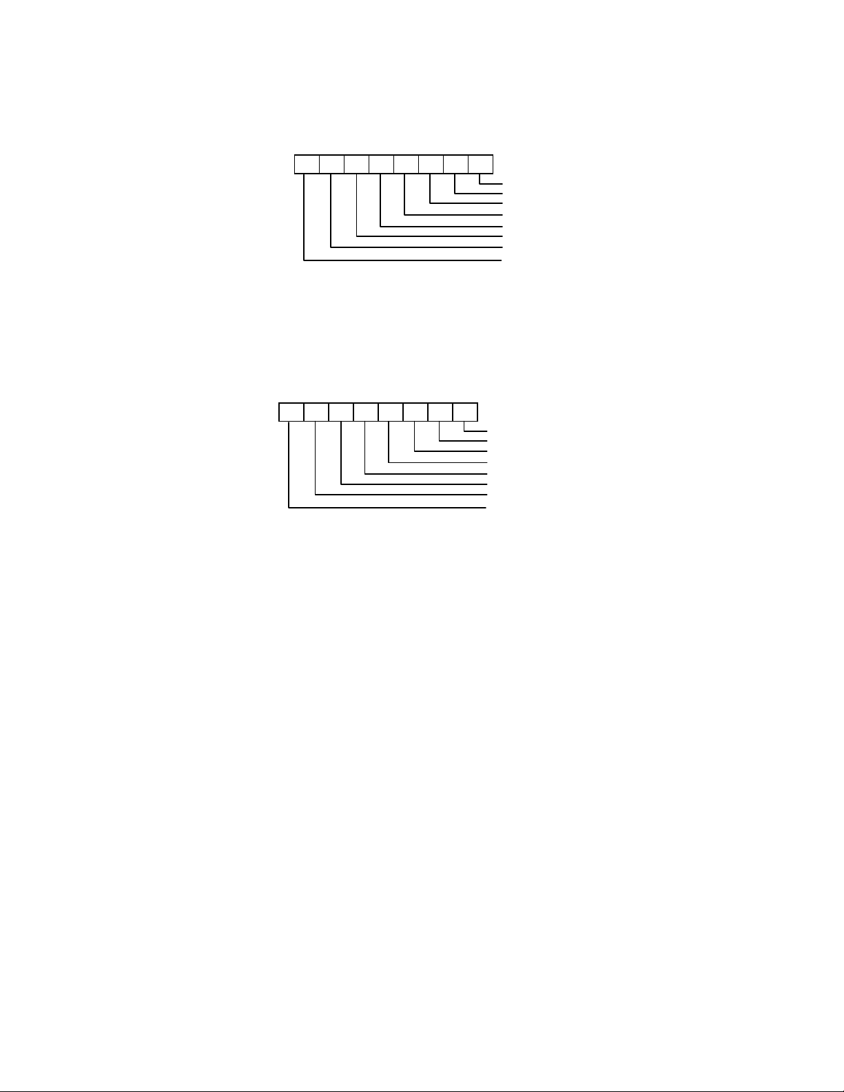
nSMI Mask Register 1
Index 43h
!!!!
Register Location: 43h
Power on Default Value 00h
Attribute: Read/Write
Size: 8 bits
7 6 5 4 3 2 1 0
VCOREA
VINRO
+3.3VIN
+5VIN
TEMP1
TEMP2
FAN1
FAN2
Bit 7-0: A one disables the corresponding interrupt status bit for nSMI interrupt.
nSMI Mask Register 2
Index 44h
!!!!
Register Location: 44h
Power on Default Value 00h
Attribute: Read/Write
Size: 8 bits
7 6 5 4 3 2 1 0
+12VIN
-12VIN
-5VIN
FAN3
Chassis Intrusion
TEMP3
Reserved
Reserved
Bit 7-6: Reserved. This bit should be set to 0.
Bit 5-0: A one disables the corresponding interrupt status bit for nSMI interrupt.
29
Page 30
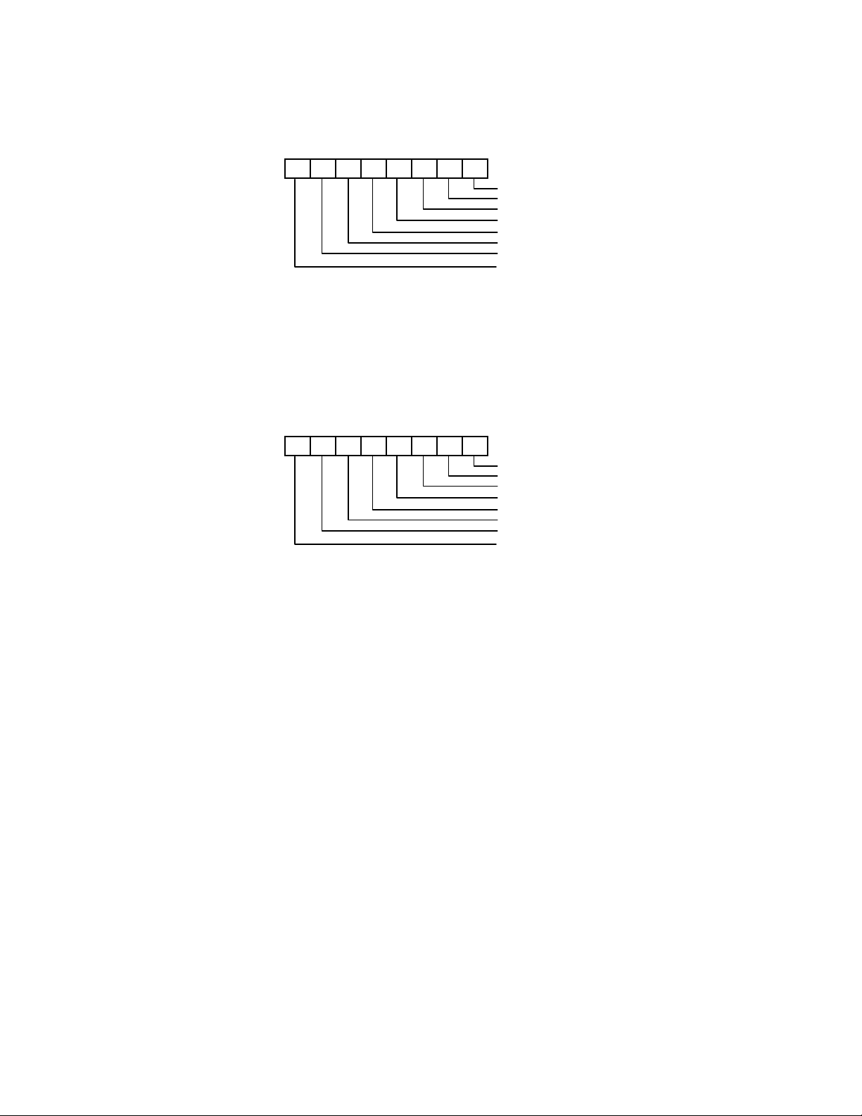
Reserved Register
Index 45h
!!!!
Chassis Clear Register -- Index 46h
Register Location: 46h
Power on Default Value <7:0> = 00000000 binary
Attribute: Read/Write
Size: 8 bits
7 6 5 4 3 2 1 0
Reserved
Reserved
Reserved
Reserved
Reserved
Reserved
Reserved
Chassis Clear
Bit 7: Set to 1, clear Chassis Intrusion event. This bit self clears after clearing Chassis Intrusion event.
Bit 6-0:Reserved. This bit should be set to 0.
VID/Fan Divisor Register
Index 47h
!!!!
Register Location: 47h
Power on Default Value <7:4> is 0101, <3:0> is mapped to VID<3:0>
Attribute: Read/Write
Size: 8 bits
7 6 5 4 3 2 1 0
VID0
VID1
VID2
VID3
FAN1DIV_B0
FAN1DIV_B1
FAN2DIV_B0
FAN2DIV_B1
Bit 7-6: FAN2 Speed Control.
Bit 5-4: FAN1 Speed Control.
Bit 3-0: The VID <3:0> inputs
Note: Please refer to Bank0 CR[5Dh] , Fan divisor table.
30
Page 31
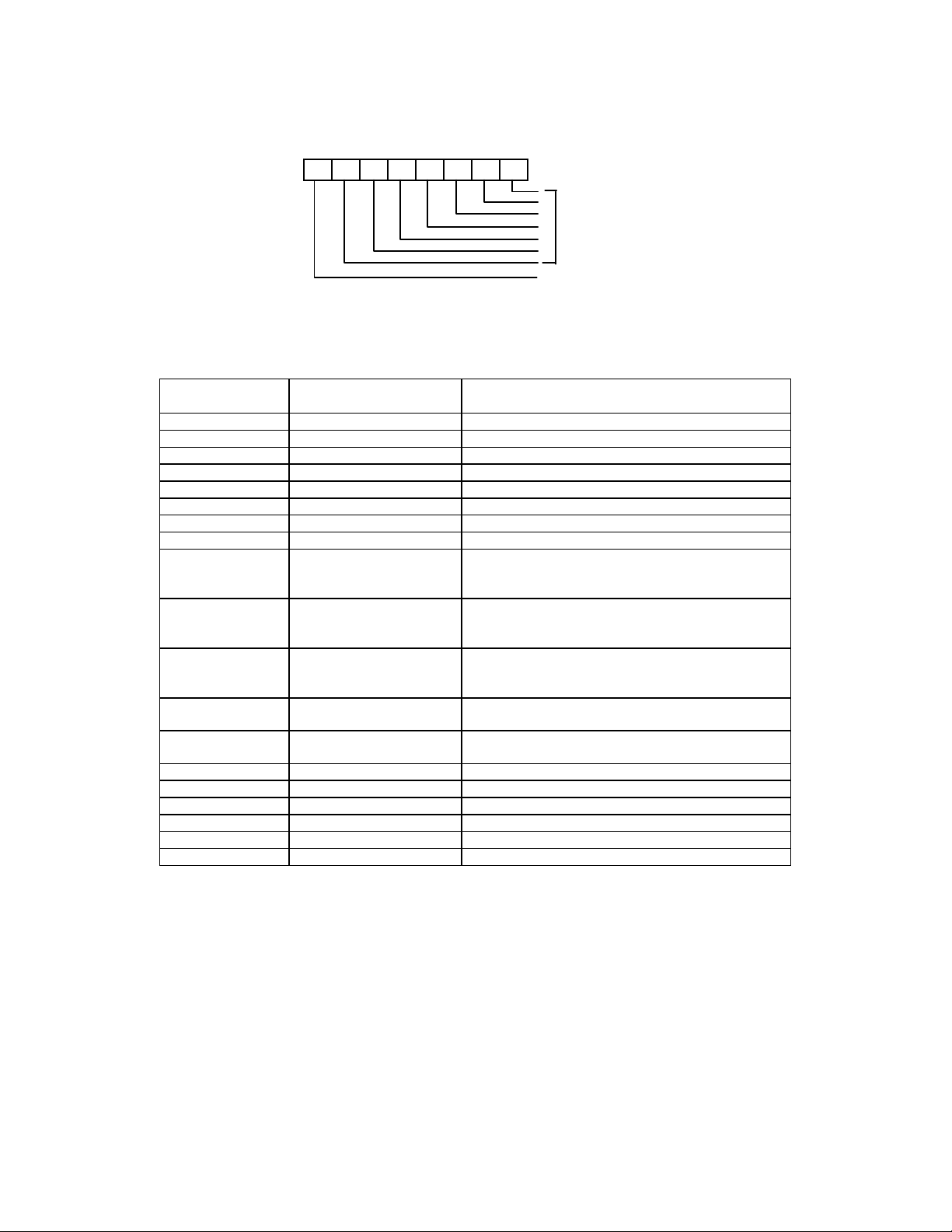
Serial Bus Address Register
Index 48h
!!!!
Register Location: 48h
Power on Default Value Serial Bus address <6:0> = 0101101 and <7> = 0 binary
Size: 8 bits
7 6 5 4 3 2 1 0
Serial Bus Address
Reserved
Bit 7: Read Only - Reserved.
Bit 6-0: Read/Write - Serial Bus address <6:0>
Value RAM
ADDRESS A6-A0
Index 20h- 3Fh or 60h - 7Fh (auto-increment)
!!!!
ADDRESS A6-A0 WITH
AUTO-INCREMENT
20h
21h
60h
61h
VCOREA reading
VINR0 reading
DESCRIPTION
22h 62h +3.3VIN reading
23h 63h +5VIN reading
24h 64h +12VIN reading
25h 65h -12VIN reading
26h 66h -5VIN reading
27h 67h Temperature reading
28h 68h FAN1 reading
Note:
This location stores the number of counts
of the internal clock per revolution.
29h 69h FAN2 reading
Note:
This location stores the number of counts
of the internal clock per revolution.
2Ah 6Ah FAN3 reading
Note:
This location stores the number of counts
of the internal clock per revolution.
2Bh 6Bh VCOREA High Limit, default value is defined by
Vcore Voltage +0.2v.
2Ch 6Ch VCOREA Low Limit, default value is defined by
Vcore Voltage -0.2v.
2Dh 6Dh VINR0 High Limit.
2Eh 6Eh VINR0 Low Limit.
2Fh 6Fh +3.3VIN High Limit
30h 70h +3.3VIN Low Limit
31h 71h +5VIN High Limit
32h 72h +5VIN Low Limit
31
Page 32
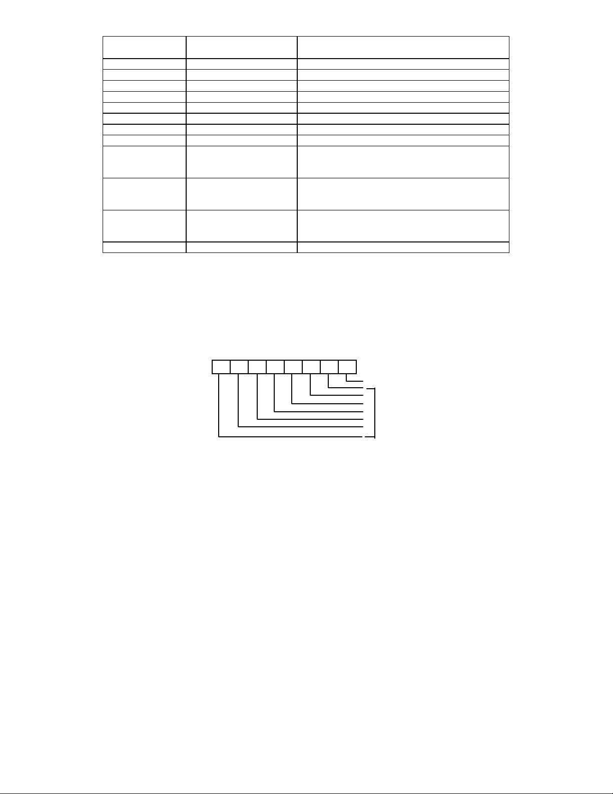
ADDRESS A6-A0
ADDRESS A6-A0 WITH
AUTO-INCREMENT
DESCRIPTION
33h 73h +12VIN High Limit
34h 74h +12VIN Low Limit
35h 75h -12VIN High Limit
36h 76h -12VIN Low Limit
37h 77h -5VIN High Limit
38h 78h -5VIN Low Limit
39h 79h Temperature sensor 1 (VTIN1) High Limit
3Ah 7Ah Temperature sensor 1 (VTIN1) Hysteresis Limit
3Bh 7Bh FAN1 Fan Count Limit
Note:
It is the number of counts of the internal
clock for the Low Limit of the fan speed.
3Ch
3Dh
7Ch
7Dh
FAN2 Fan Count Limit
Note:
It is the number of counts of the internal
clock for the Low Limit of the fan speed.
FAN3 Fan Count Limit
Note:
It is the number of counts of the internal
clock for the Low Limit of the fan speed.
3E- 3Fh 7E- 7Fh Reserved
Setting all ones to the high limits for voltages and fans (0111 1111 binary for temperature) means
interrupts will never be generated except the case when voltages go below the low limits.
Voltage ID (VID4) & Device ID -- Index 49h
Register Location: 49h
Power on Default Value <7:1> is 000,0001b
<0> is mapped to VID <4>
Size: 8 bits
7 6 5 4 3 2 1 0
Bit 7-1: Read Only - Device ID<6:0>
Bit 0 : Read/Write - The VID4 inputs.
VID4
DID<6:0>
32
Page 33
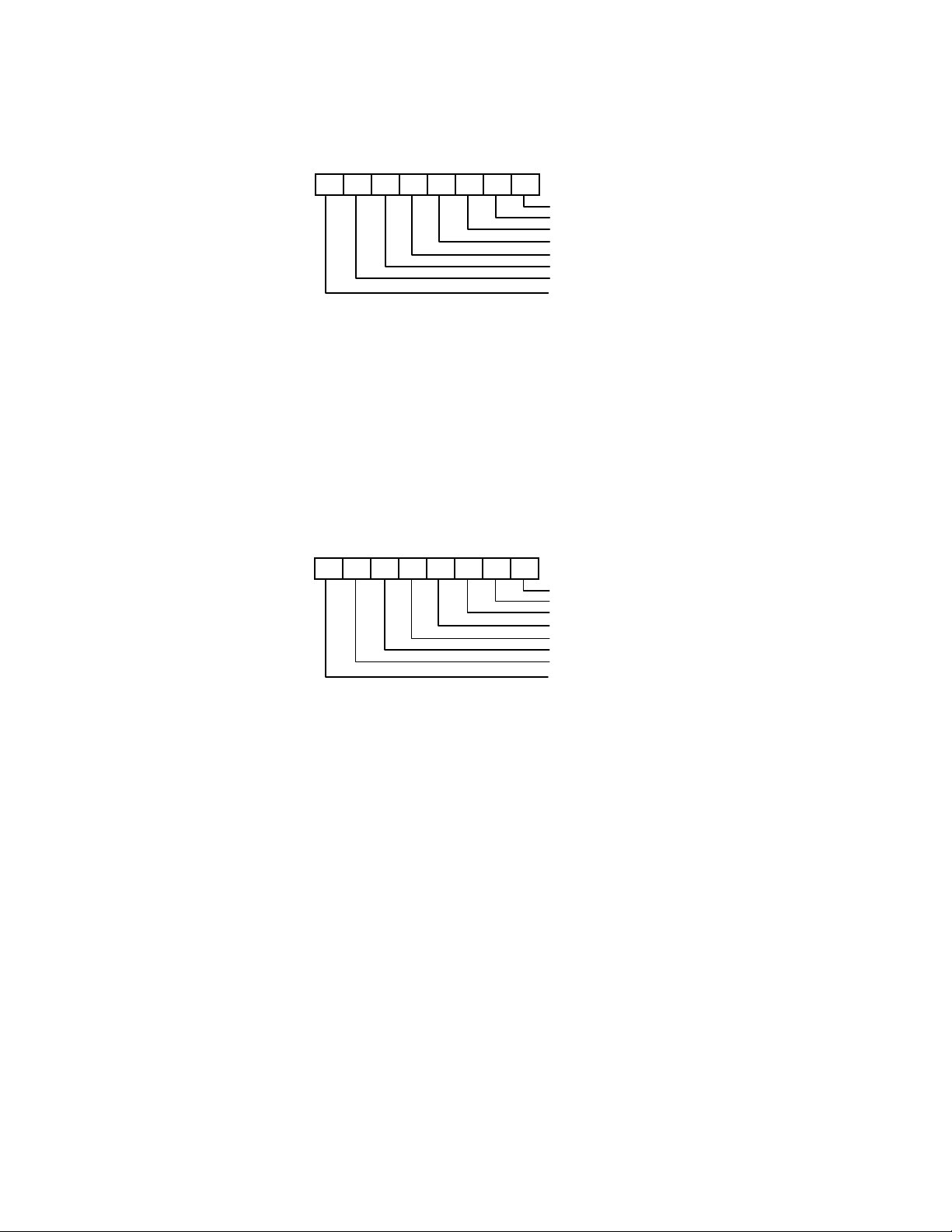
Temperature 2 and Temperature 3 Serial Bus Address Register--Index 4Ah
Register Location: 4Ah
Power on Default Value <7:0> = 0000,0001 binary. Reset by MR
Attribute: Read/Write
Size: 8 bits
7 6 5 4 3 2 1 0
I2CADDR2
I2CADDR2
I2CADDR2
DIS_T2
I2CADDR3
I2CADDR3
I2CADDR3
DIS_T3
Bit 7: Set to 1, disable temperature sensor 3 and can not access any data from Temperature Sensor 3.
Bit 6-4: Temperature 3 Serial Bus Address. The serial bus address is 1001xxx. W her e xxx are defi ned in
these bits.
Bit 3: Set to 1, disable temperature Sensor 2 and can not access any data from T emperature Sensor 2.
Bit 2-0: Temperature 2 Serial Bus Address. The serial bus address is 1001xxx. Wh ere xxx are d efi ned in
these bits.
Pin Control Register -- Index4Bh
Register Location: 4Bh
Power on Default Value <7:0> 44h. Reset by MR.
Attribute: Read/Write
Size: 8 bits
7 6 5 4 3 2 1 0
Reserved
Reserved
CLKINSEL
CLKINSEL
ADCOVSEL
ADCOVSEL
FAN3DIV_B0
FAN3DIV_B1
Bit 7-6:Fan3 speed divisor.
Please refer to Bank0 CR[5Dh] , Fan divisor table.
Bit 5-4: Select A/D Converter Clock Input.
<5:4> = 00 - default. ADC clock select 22.5 kHz.
<5:4> = 01- ADC clock select 5.6 kHz. (22.5K/4)
<5:4> = 10 - ADC clock select 1.4kHz. (22.5K/16)
<5:4> = 11 - ADC clock select 0.35 kHz. (22.5K/64)
Bit 3-2: Clock Input Select.
33
Page 34

<3:2> = 00 - Pin 3 (CLKIN) select 14.318MHz clock.
<3:2> = 01 - Default. Pin 3 (CLKIN) select 24MHz clock.
<3:2> = 10 - Pin 3 (CLKIN) select 48MHz clock .
<3:2> = 11 - Reserved. Pin 3 no clock input.
Bit 1-0: Reserved. User defined.
nIRQ/nOVT Property Select -- Index 4Ch
Register Location: 4Ch
Power on Default Value <7:0> --0000,0001. Reset by MR.
Attribute: Read/Write
Size: 8 bits
7 6 5 4 3 2 1 0
Reserved
Reserved
OVTPOL
DIS_OVT1
DIS_OVT2
Reserved
T23_INTMode
Reserved
Bit 7: Reserved. User Defined.
Bit6: Set to 1, the nSMI output type of Temperature 2 and 3 is set to Comparator Interrupt mode. Set
to 0, the nSMI output type is set to Two-Times Interrupt mode. (default 0)
Bit5: Reserved. User Defined.
Bit 4: Disable temperature sensor 3 over-temperature (OVT) output if set to 1. Default 0, enable OVT2
output through pin nOVT.
Bit 3: Disable temperature sensor 2 over-temperature (OVT) output if set to 1. Default 0, enable
OVT1 output through pin nOVT.
Bit 2: Over-temperature polarity. If this bit is 1, nOVT active high. If this bit is 0, nOVT active low.
Default 0.
Bit 1: Reserved. User Defined.
Bit 0: Reserved. User Defined.
34
Page 35

FAN IN/OUT and BEEP/nGPO Control Register -- Index 4Dh
Register Location: 4Dh
Power on Default Value <7:0> 0001,0101. Reset by MR.
Attribute: Read/Write
Size: 8 bits
7 6 5 4 3 2 1 0
FANINC1
FANOPV1
FANINC2
FANOPV2
FANINC3
FANOPV3
GPOSEL
DIS_ABN
Bit 7: Disable power-on abnormal voltage monitoring including V-Core A and +3.3V. If these voltages
exceed the limit value, the BEEP pin (Open Drain) will drive a 300Hz or 600Hz frequency signal.
If this bit is 1, the frequency will be disable. Default 0. After power on, the system should set 1
to this bit to 1 in order to disable BEEP.
Bit 6: BEEP/nGPO Pin Function Select. If this bit is 1 Select nGPO function. Set 0, select BEEP
function. This bit defaults to 0.
Bit 5: FAN 3 output value if FANINC3 is set to 0. If this bit is 1, then pin 18 always generate logic high
signal. If this bit is 0, pin 18 always generates logic low signal. This bit default 0.
Bit 4: FAN 3 Input Control. Set to 1, pin 18 acts as FAN clock input, which is default value. Set to 0,
this pin 18 acts as FAN control signal and the output value of FAN control is set by this register
bit 5. This output pin can connect to power PMOS gate to control FAN ON/OFF.
Bit 3: FAN 2 output value if FANINC2 sets to 0. If this bit is 1, then pin 19 always generate logic high
signal. If this bit is 0, pin 19 always generates logic low signal. This bit default 0.
Bit 2: FAN 2 Input Control. Set to 1, pin 19 acts as FAN clock input, which is default value. Set to 0,
this pin 19 acts as FAN control signal and the output value of FAN control is set by this register
bit 3. This output pin can connect to power NMOS gate to control FAN ON/OFF.
Bit 1: FAN 1 output value if FANINC1 sets to 0. If this bit is 1, then pin 20 always generate logic high
signal. If this bit is 0, pin 20 always generates logic low signal. This bit default 0.
Bit 0: FAN 1 Input Control. Set to 1, pin 20 acts as FAN clock input, which is default value. Set to 0,
this pin 20 acts as FAN control signal and the output value of FAN control is set by this register t
1. This output pin can connect to power PMOS gate to control FAN ON/OFF.
35
Page 36
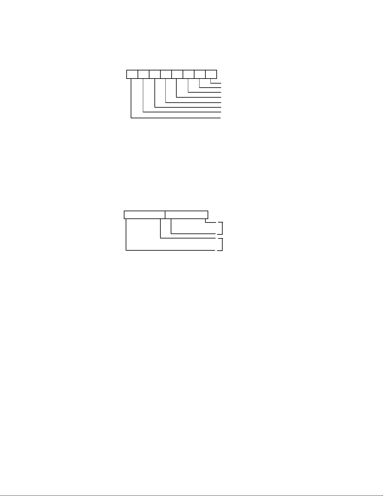
Register 50h ~ 5Fh Bank Select -- Index 4Eh
Register Location: 4Eh
Power on Default Value <6:3> = Reserved, <7> = 1, <2:0> = 0. Reset by MR
Attribute: Read/Write
Size: 8 bits
7 6 5 4 3 2 1 0
BANKSEL0
BANKSEL1
BANKSEL2
Reserved
Reserved
Reserved
Reserved
HBACS
Bit 7: HBACS- High byte access. Set to 1, access Register 4Fh high byte register.
Set to 0, access Register 4Fh low byte register. Default 1.
Bit 6-3: Reserved. This bit should be set to 0.
Bit 2-0: Index ports 0x50~0x5F Bank select.
SMSC Vendor ID -- Index 4Fh
Register Location: 4Fh
Power on Default Value <15:0> = 5CA3h
Attribute: Read Only
Size: 16 bits
15 8 7 0
VIDH
VIDL
Bit 15-8: Vendor ID High Byte if CR4E.bit7=1.Default 5Ch.
Bit 7-0: Vendor ID Low Byte if CR4E.bit7=0. Default A3h.
36
Page 37

SMSC Test Register -- Index 50h - 55h (Bank 0)
BEEP Control Register 1-- Index 56h (
Bank 0
)
Register Location: 56h
Power on Default Value <7:0> 0000,0000. Reset by MR.
Attribute: Read/Write
Size: 8 bits
7 6 5 4 3 2 1 0
EN_VCA_BP
EN_Vr0_BP
EN_V33_BP
EN_V5_BP
EN_T1_BP
EN_T2_BP
EN_FAN1_BP
EN_FAN2_BP
Bit 7: Enable BEEP Output from FAN 2 if the monitor value exceed the limit value. If this bit is 1
(default), enable BEEP output.
Bit 6: Enable BEEP Output from FAN 1 if the monitor value exceed the limit value. If this bit is 1
(default),, enable BEEP output.
Bit 5: Enable BEEP Output from Temperature Sensor 2 if the monitor value exceed the limit value.
If this bit is 1, enable BEEP output. Default 0
Bit 4: Enable BEEP output for Temperature Sensor 1 if the monitor value exceed the limit value. If
this bit is 1, enable BEEP output. Default 0
Bit 3: Enable BEEP output from VDD (+5V), If this bit is 1, enable BEEP output if the monitor value
exceed the limits value. Default 0, disable BEEP output.
Bit 2: Enable BEEP output from +3.3V. If this bit is 1, enable BEEP output. Default 1.
Bit 1: Enable BEEP output from VINR0. If this bit is 1, enable BEEP output. Default 1.
Bit 0: Enable BEEP Output from VCOREA if the monitor value exceeds the limits value. If this bit is 1,
enable BEEP output. Default 1.
37
Page 38
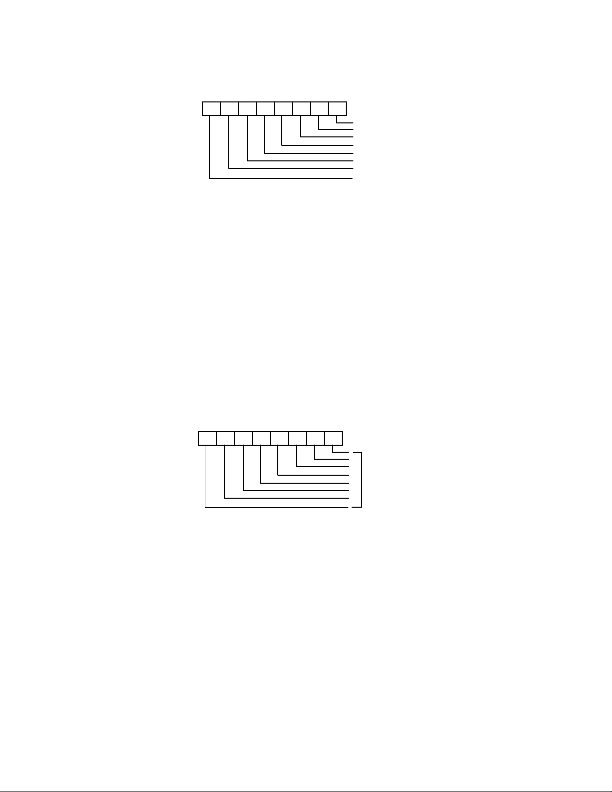
BEEP Control Register 2-- Index 57h (
Bank 0
)
Register Location: 57h
Power on Default Value <7:0> 1000-0000. Reset by MR.
Attribute: Read/Write
Size: 8 bits
7 6 5 4 3 2 1 0
EN_V12_BP
EN_NV12_BP
EN_NV5_BP
EN_FAN3_BP
EN_CASO_BP
EN_T3_BP
Reserved
EN_GBP
Bit 7: Enable Global BEEP. If this bit is 1, enable global BEEP output. Default 1. If this bit is 0, disable
all BEEP outputs.
Bit 6: Reserved. This bit should be set to 0.
Bit 5: Enable BEEP Output from Temperature Sensor 3 if the monitor value exceed the limit value.
If this bit is 1, enable BEEP output. Default 0
Bit 4: Enable BEEP output for case open if the monitor value exceed the limit value. If this bit is 1,
enable BEEP output. Default 0.
Bit 3: Enable BEEP Output from FAN 3 if the monitor value exceed the limit value. If this bit is 1,
enable BEEP output. Default 0.
Bit 2: Enable BEEP output from -5V, If this bit is 1, enable BEEP output if the monitor value exceed
the limits value. Default 0, disable BEEP output.
Bit 1: Enable BEEP output from -12V, If this bit is 1, enable BEEP output if the monitor value exceed
the limits value. Default 0, disable BEEP output.
Bit 0: Enable BEEP output from +12V, If this bit is 1, enable BEEP output if the monitor value exceed
the limits value. Default 0, disable BEEP output.
Chip ID -- Index 58h (
Bank 0
)
Register Location: 58h
Power on Default Value <7:0> 0011-0000. Reset by MR.
Attribute: Read Only
Size: 8 bits
7 6 5 4 3 2 1 0
CHIPID
Bit 7: SMSC Chip ID number. Read this register will return 30h.
38
Page 39
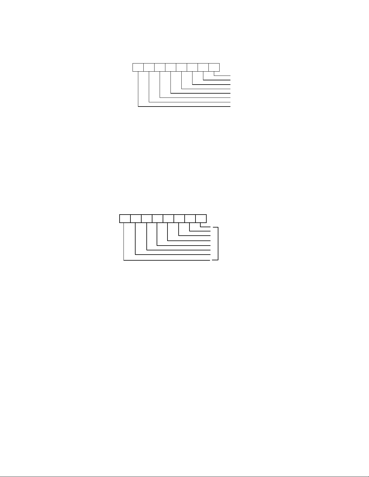
Diode Selection Register -- Index 59h (Bank 0)
Register Location: 59h
Power on Default Value <7>=0 and <6:4> = 111 and <3:0> = 0000
Attribute: Read/Write
Size: 8 bits
7 6 5 4 3 2 1 0
Reserved
Reserved
Reserved
Reserved
SELPIIV1
SELPIIV2
SELPIIV3
Reserved
Bit 7: Reserved
Bit 6: Temperature sensor diode 3. Set to 1, select Pentium II compatible Diode. Set to 0 to
select 2N3904 Bipolar mode.
Bit 5: Temperature sensor diode 2. Set to 1, select Pentium II compatible Diode. Set to 0 to
select 2N3904 Bipolar mode.
Bit 4: Temperature sensor diode 1. Set to 1, select Pentium II compatible Diode. Set to 0 to
select 2N3904 Bipolar mode.
Bit 3-0: Reserved
PWMOUT2 Control -- Index 5Ah (Bank 0)
Register Location: 5Ah
Power on default value: <7:0> 1111-1111. Reset by MR.
Attribute: Read/Write
Size: 8 bits
7 6 5 4 3 2 1 0
Bit 7: PWMOUT2 duty cycle control
If this is FF, Duty cycle is 100%, If this is 00, Duty cycle is 0%.
39
PWM2_DUTY
Page 40

PWMOUT1 Control -- Index 5Bh (
Bank 0
)
Register Location: 5Bh
Power on default value: <7:0> 1111-1111. Reset by MR.
Attribute: Read/Write
Size: 8 bits
7 6 5 4 3 2 1 0
PWM1_DUTY
Bit 7: PWMOUT1 duty cycle control
If this is FF, Duty cycle is 100%,
If this is 00, Duty cycle is 0%.
40
Page 41
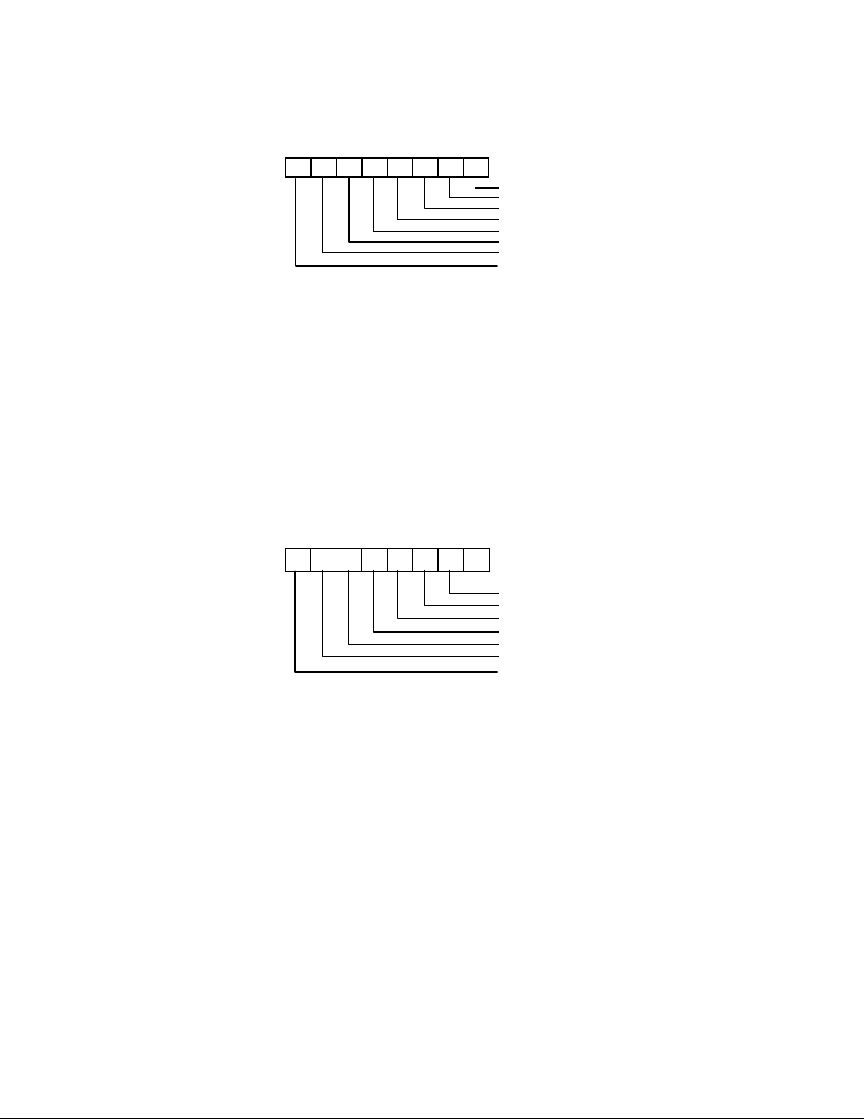
PWMOUT1/2 Clock Select -- Index 5Ch (
Bank 0
)
Register Location: 5Ch
Power on Default Value <7:0> 0001-0001. Reset by MR.
Attribute: Read/Write
Size: 8 bits
7 6 5 4 3 2 1 0
PWM2CLKSEL
PWM2CLKSEL
PWM2CLKSEL
EN_FANPWM2
PWM1CLKSEL
PWM1CLKSEL
PWM1CLKSEL
Reserved
Bit 7: Reserved
Bit 6-4: PWMOUT1 clock selection.
The clock frequency definition is the same as PWMOUT2 clock selection.
Bit 3: Set to 1. Enable PWMOUT2 PWM Control
Bit 2-0: PWMOUT2 clock Selection.
<2:0> = 000: 46.87KHz
<2:0> = 001: 23.43KHz (Default)
<2:0> = 010: 11.72KHz
<2:0> = 011: 5.85KHz
<2:0> = 100: 2.93KHz
VBAT Monitor Control Register -- Index 5Dh (
Bank 0
)
Register Location: 5Dh
Power on Default Value <7:0> 0000-0000. Reset by MR.
Attribute: Read/Write
Size: 8 bits
7 6 5 4 3 2 1 0
EN_VBAT_M NT
DIODES1
DIODES2
DIOD E S 3
Reserved
FANDIV1_B2
FANDIV2_B2
FANDIV3_B2
Bit 7: Fan3 divisor Bit 2.
Bit 6: Fan2 divisor Bit 2.
Bit 5: Fan1 divisor Bit 2.
Bit 4: Reserved.
Bit 3: Temperature sensor 3 select into thermal diode such as Pentium II CPU supported. Set to 1,
select bipolar sensor. Set to 0, select thermistor sensor.
Bit 2: Sensor 2 type selection. Defined as DIODES3 described in the bit 3.
41
Page 42
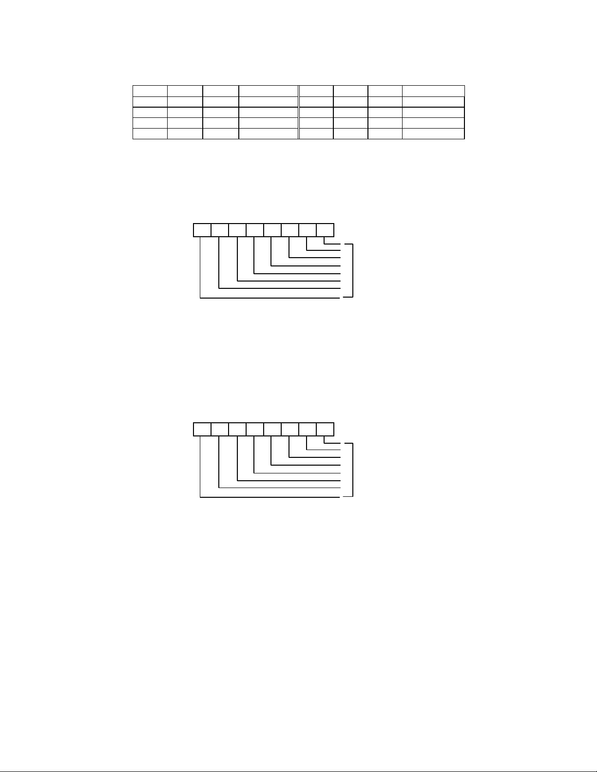
Bit 1: Sensor 1 type selection. Defined as DIODES2 described in the bit 3.Bit 0: Set to 1, enable
battery voltage monitor. Set to 0, disable battery voltage monitor. If enabled, the monitor value is
after one monitor cycle. Note that the monitor cycle time is at least 300ms for MON35W42.
FAN DIVISOR TABLE
Bit 2 Bit 1 Bit 0 Fan Divisor Bit 2 Bit 1 Bit 0 Fan Divisor
0 0 0 1 1 0 0 16
0 0 1 2 1 0 1 32
0 1 0 4 1 1 0 64
0 1 1 8 1 1 1 128
PWMOUT3 Control -- Index 5Eh (
Bank 0
)
Register Location: 5Eh
Power on Default Value <7:0> 1111-1111. Reset by MR.
Attribute: Read/Write
Size: 8 bits
7 6 5 4 3 2 1 0
PWM3_DUTY
Bit 7: PWMOUT3 duty cycle control
If this is FF, Duty cycle is 100%,
If this is 00, Duty cycle is 0%.
PWMOUT4 Control -- Index 5Fh (
Bank 0
)
Register Location: 5Fh
Power on Default Value <7:0> 1111-1111. Reset by MR.
Attribute: Read Only
Size: 8 bits
7 6 5 4 3 2 1 0
PWM4_DUTY
Bit 7: PWMOUT4 duty cycle control
If this is FF, Duty cycle is 100%,
If this is 00, Duty cycle is 0%.
42
Page 43

Temperature Sensor 2 Temperature (High Byte) Register - Index 50h (
Register Location: 50h
Attribute: Read Only
Size: 8 bits
7 6 5 4 3 2 1 0
TEMP2<8:1>
Bank 1
)
Bit 7: Temperature <8:1> of sensor 2, which is high byte.
Temperature Sensor 2 Temperature (Low Byte) Register - Index 51h (
Register Location: 51h
Attribute: Read Only
Size: 8 bits
7 6 5 4 3 2 1 0
Reserved
TEMP2<0>
Bit 7: Temperature <0> of sensor2, which is low byte.
Bit 6-0: Reserved. This bit should be set to 0.
Bank 1
)
43
Page 44
Temperature Sensor 2 Configuration Register - index 52h (
Register Location: 52h
Power on Default Value <7:0> = 0x00
Size: 8 bits
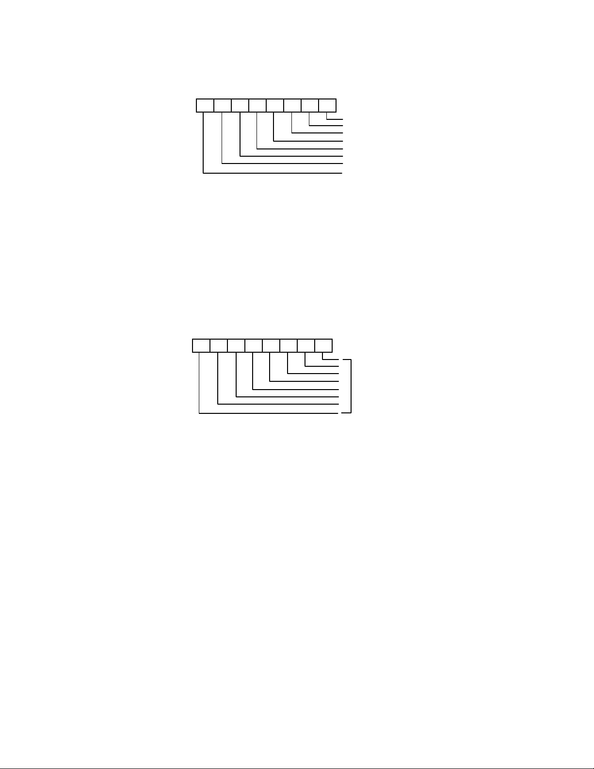
7 6 5 4 3 2 1 0
Bank 1
STOP2
INTMOD
Reserved
FAULT
FAULT
Reserved
Reserved
Reserved
)
Bit 7-5: Read - Reserved. This bit should be set to 0.
Bit 4-3: Read/Write - Number of faults to detect before setting nOVT output to avoid false tripping
due to noise.
Bit 2: Read - Reserved. This bit should be set to 0.
Bit 1: Read/Write - nOVT Interrupt mode select. This bit default is set to 0, which is compared
mode. When set to 1, interrupt mode will be selected.
Bit 0: Read/Write - When set to 1 the sensor will stop monitoring.
Temperature Sensor 2 Hysteresis (High Byte) Register - Index 53h (
Bank 1
)
Register Location: 53h
Power on Default Value <7:0> = 0x4B
Attribute: Read/Write
Size: 8 bits
7 6 5 4 3 2 1 0
THYST2<8:1>
Bit 7-0: Temperature hysteresis bit 8-1, which is High Byte. The temperature default 75 degree C.
44
Page 45
Temperature Sensor 2 Hysteresis (Low Byte) Register - Index 54h (
Register Location: 54h
Power on Default Value <7:0> = 0x0
Attribute: Read Only
Size: 8 bits
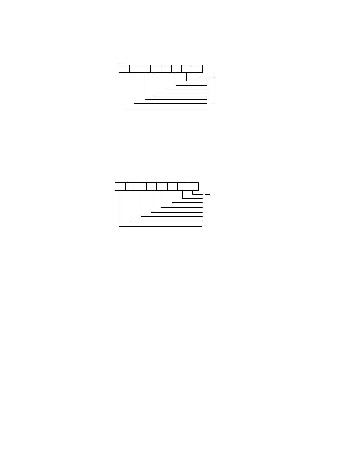
7 6 5 4 3 2 1 0
Reserved
Bank 1
)
THYST2<0>
Bit 7: Temperature hysteresis bit 0, which is low Byte.
Bit 6-0: Reserved. This bit should be set to 0.
Temperature Sensor 2 Over-temperature (High Byte) Register - Index 55h (
Bank 1
)
Register Location: 55h
Power on Default Value <7:0> = 0x50
Attribute: Read/Write
Size: 8 bits
7 6 5 4 3 2 1 0
TOVF2<8:1>
Bit 7-0: Over-temperature bit 8-1, which is High Byte. The temperature default 80 degree C.
45
Page 46
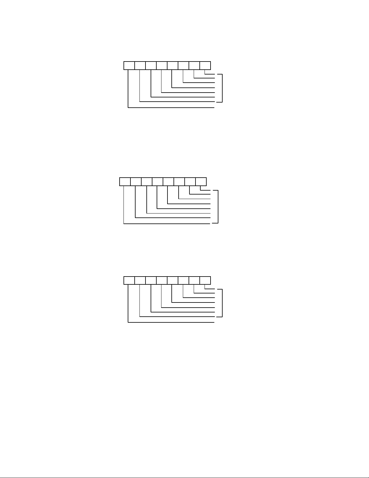
Temperature Sensor 2 Over-temperature (Low Byte) Register - Index 56h(
Register Location: 56h
Power on Default Value <7:0> = 0x0
Size: 8 bits
7 6 5 4 3 2 1 0
Reserved
Bank 1
)
TOVF2<0>
Bit 7: Read/Write - Over-temperature bit 0, which is low Byte.
Bit 6-0: Read Only - Reserved. This bit should be set to 0.
Temperature Sensor 3 Temperature (High Byte) Register - Index 50h (
Register Location: 50h
Attribute: Read Only
Size: 8 bits
7 6 5 4 3 2 1 0
TEMP2<8:1>
Bit 7-0: Temperature <8:1> of sensor 2, which is high byte.
Temperature Sensor 3 Temperature (Low Byte) Register - Index 51h (
Register Location: 51h
Attribute: Read Only
Size: 8 bits
7 6 5 4 3 2 1 0
Bank 2
Bank 2
)
)
Bit 7: Temperature <0> of sensor2, which is low byte.
Bit 6-0: Reserved. This bit should be set to 0.
46
Reserved
TEMP2<0>
Page 47
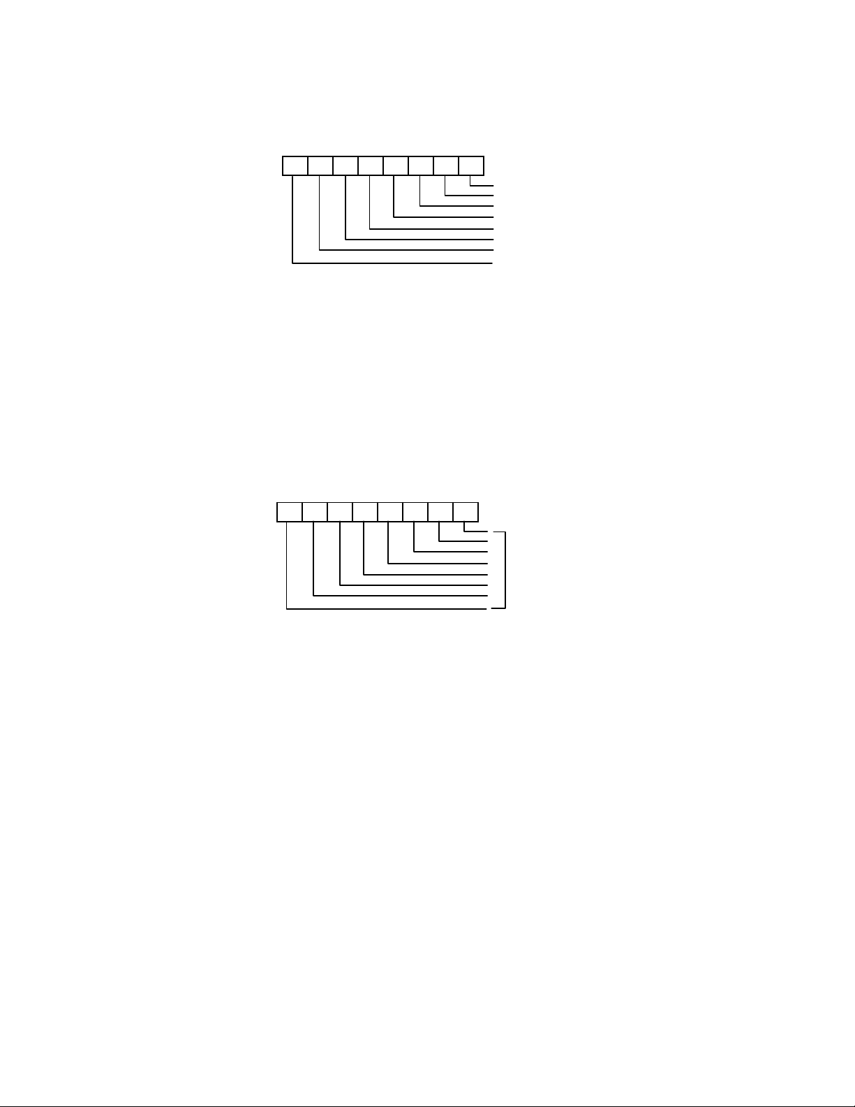
Temperature Sensor 3 Configuration Register - Index 52h (
Register Location: 52h
Power on Default Value <7:0> = 0x00
Size: 8 bits
7 6 5 4 3 2 1 0
Bank 2
STOP3
INTMOD
Reserved
FAULT
FAULT
Reserved
Reserved
Reserved
)
Bit 7-5: Read - Reserved. This bit should be set to 0.
Bit 4-3: Read/Write - Number of faults to detect before setting nOVT output to avoid false tripping
due to noise.
Bit 2: Read - Reserved. This bit should be set to 0.
Bit 1: Read/Write - nOVT Interrupt Mode select. This bit default is set to 0, which is Compared
Mode. When set to 1, Interrupt Mode will be selected.
Bit 0: Read/Write - When set to 1 the sensor will stop monitoring.
Temperature Sensor 3 Hysteresis (High Byte) Register - Index 53h (
Bank 2
)
Register Location: 53h
Power on Default Value <7:0> = 0x4B
Attribute: Read/Write
Size: 8 bits
7 6 5 4 3 2 1 0
THYST3<8:1>
Bit 7-0: Temperature hysteresis bit 8-1, Bit 8 is the MSB. The temperature default 75 degree C.
47
Page 48
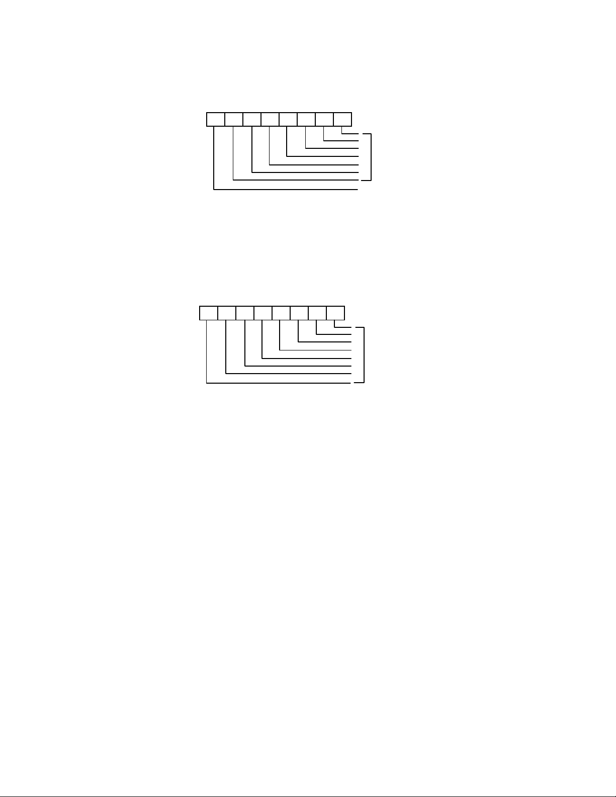
Temperature Sensor 3 Hysteresis (Low Byte) Register - Index 54h (
Register Location: 54h
Power on Default Value <7:0> = 0x0
Attribute: Read Only
Size: 8 bits
7 6 5 4 3 2 1 0
Reserved
Bank 2
)
THYST3<0>
Bit 7: Temperature hysteresis bit 0, this is the LSB.
Bit 6-0: Reserved. This bit should be set to 0.
Temperature Sensor 3 Over-temperature (High Byte) Register - Index 55h (
Bank 2
)
Register Location: 55h
Power on Default Value <7:0> = 0x50
Attribute: Read/Write
Size: 8 bits
7 6 5 4 3 2 1 0
TOVF3<8:1>
Bit 7-0: Over-temperature bit 8-1, bit 8 is the MSB. The temperature default 80 degree C.
48
Page 49
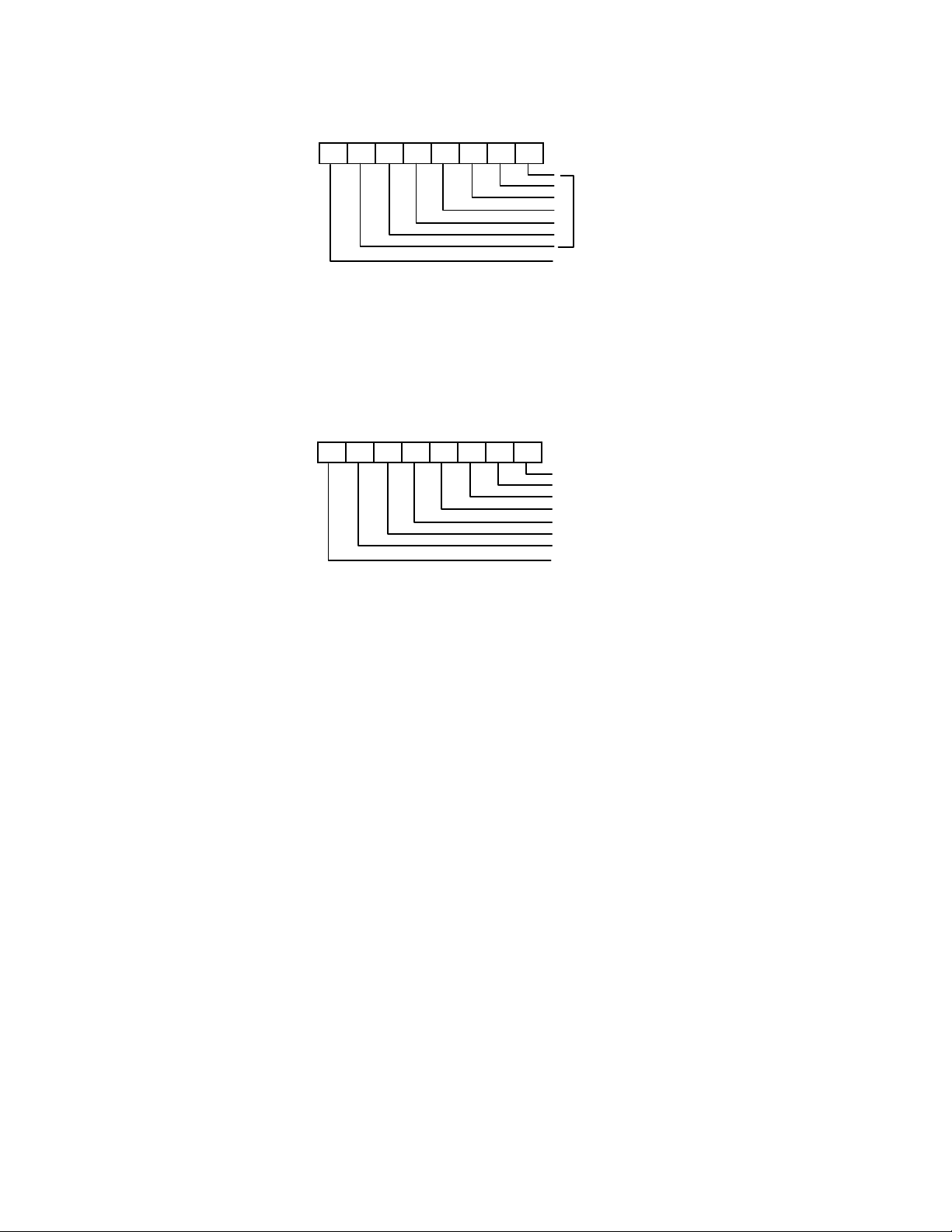
Temperature Sensor 3 Over-temperature (Low Byte) Register - Index 56h(
Register Location: 56h
Power on Default Value <7:0> = 0x0
Size: 8 bits
7 6 5 4 3 2 1 0
Reserved
Bank 2
)
TOVF3<0>
Bit 7: Read/Write - Over-temperature bit 0, this is the LSB.
Bit 6-0: Read Only - Reserved. This bit should be set to 0.
Interrupt Status Register 3 -- Index 50h (BANK4)
Register Location: 50h
Power on Default Value <7:0> = 00h
Attribute: Read Only
Size: 8 bits
7 6 5 4 3 2 1 0
5VSB
VBAT
Reserved
Reserved
Reserved
Reserved
Reserved
Reserved
Bit 7-2: Reserved.
Bit 1: A one indicates a High or Low limit of VBAT has been exceeded.
Bit 0: A one indicates a High or Low limit of 5VSB has been exceeded.
49
Page 50
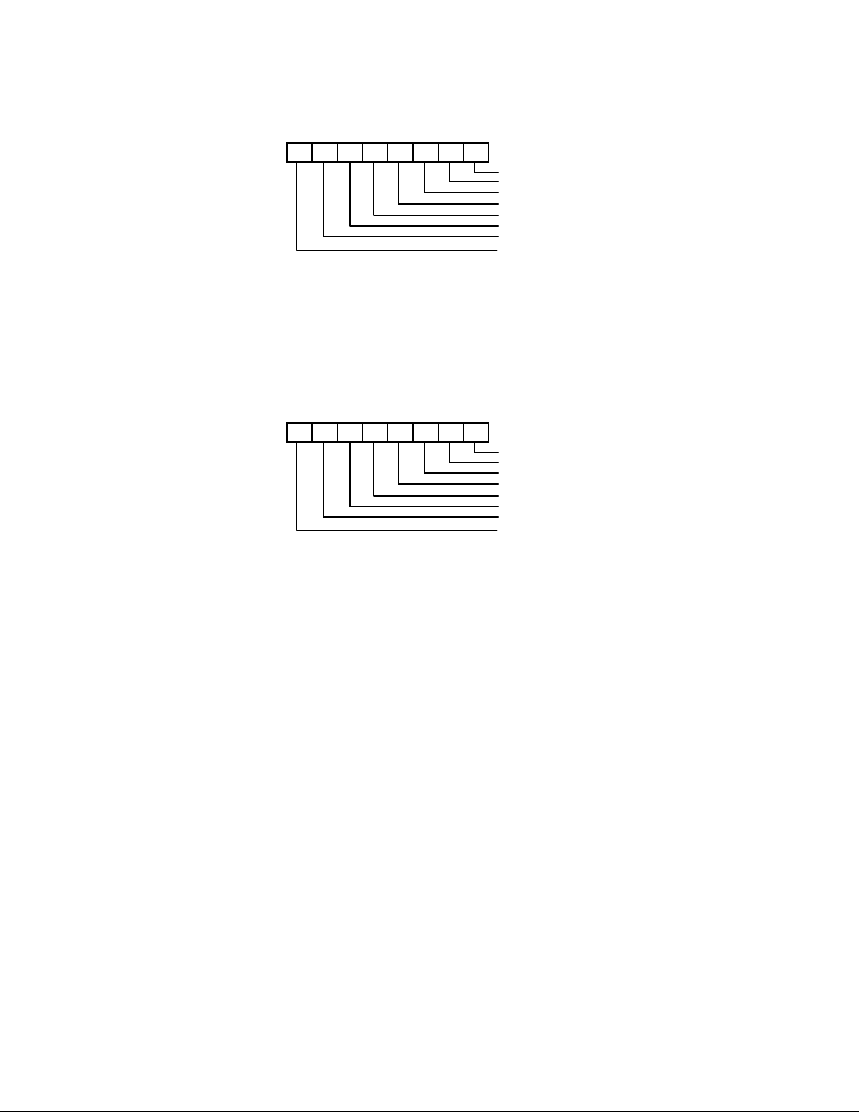
nSMI Mask Register 3 -- Index 51h (BANK 4)
Register Location: 51h
Power on Default Value <7:0> = 0000,0000h
Attribute: Read/Write
Size: 8 bits
7 6 5 4 3 2 1 0
5VSB
VBAT
Reserved
Reserved
Reserved
Reserved
Reserved
Reserved
Bit 7-2: Reserved.
Bit 1: A one disables the corresponding interrupt status bit for nSMI interrupt.
Bit 0: A one disables the corresponding interrupt status bit for nSMI interrupt.
BEEP Control Register 3-- Index 53h (
Bank 4
)
Register Location: 53h
Power on Default Value <7:0> 0000,0000. Reset by MR.
Attribute: Read/Write
Size: 8 bits
7 6 5 4 3 2 1 0
EN_5VSB_BP
EN_VBAT_BP
Reserved
Reserved
Reserved
EN_USER_BP
Reserved
Reserved
Bit 7-6: Reserved.
Bit 5: User define BEEP output function. If this bit is 1, the BEEP is always active. If this bit is 0, this
function is inactive. (Default 0)
Bit 4-2: Reserved.
Bit 1: Enable BEEP output from VBAT. If this bit is 1, enable BEEP output, which is default value.
Bit 0: Enable BEEP Output from 5VSB. If this bit is 1, enable BEEP output, which is default value.
50
Page 51

Reserved Register -- Index 54h--58h
Real Time Hardware Status Register I -- Index 59h (
Bank 4
)
Register Location: 59h
Power on Default Value <7:0> 0000,0000. Reset by MR.
Attribute: Read Only
Size: 8 bits
7 6 5 4 3 2 1 0
VCOREA_STS
VINR0_STS
+3.3VIN_STS
+5VIN_STS
TEMP1_STS
TEMP2_STS
FAN1_STS
FAN2_STS
Bit 7: FAN 2 Status. Set 1, the fan speed counter is over the limit value. Set 0, the fan speed counter
is in the limit range.
Bit 6: FAN 1 Status. Set 1, the fan speed counter is over the limit value. Set 0, the fan speed counter
is in the limit range.
Bit 5: Temperature sensor 2 Status. Set 1, the voltage of temperature sensor is over the limit value.
Set 0, the voltage of temperature sensor is in the limit range.
Bit 4: Temperature sensor 1 Status. Set 1, the voltage of temperature sensor is over the limit value.
Set 0, the voltage of temperature sensor is in the limit range.
Bit 3: +5V Voltage Status. Set 1, the voltage of +5V is over the limit value. Set 0, the voltage of +5V is
in the limit range.
Bit 2: +3.3V Voltage Status. Set 1, the voltage of +3.3V is over the limit value. Set 0, the voltage of
+3.3V is in the limit range.
Bit 1: VINR0 Voltage Status. Set 1, the voltage of VINR0 is over the limit value. Set 0, the voltage of
VINR0 is in the limit range.
Bit 0: VCOREA Voltage Status. Set 1, the voltage of VCORE A is over the limit value. Set 0, the
voltage of VCORE A is in the limit range.
51
Page 52
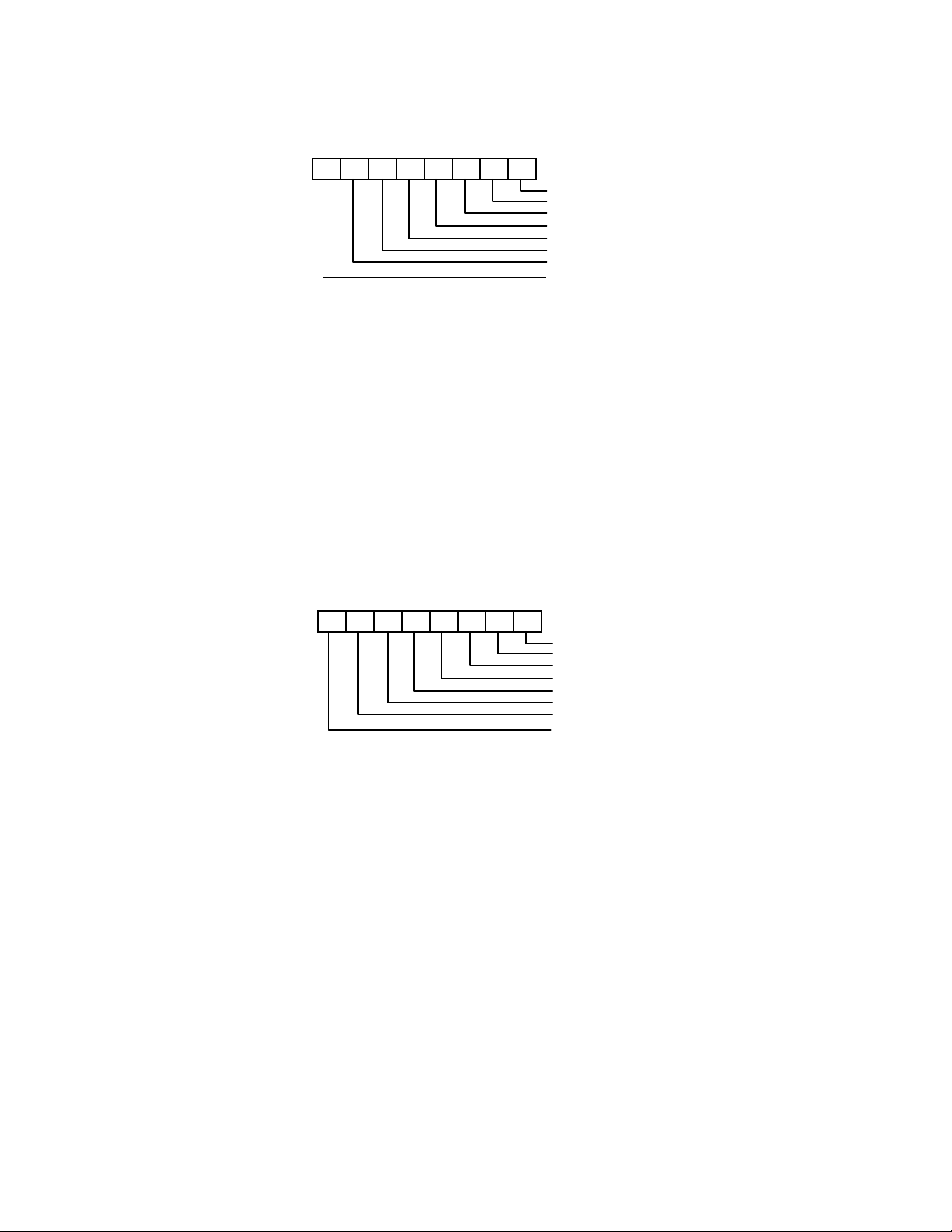
Real Time Hardware Status Register II -- Index 5Ah (
Bank 4
)
Register Location: 5Ah
Power on Default Value <7:0> 0000,0000. Reset by MR.
Attribute: Read Only
Size: 8 bits
7 6 5 4 3 2 1 0
+12VIN_STS
-12VIN_STS
-5VIN_STS
FAN3_STS
CASE_STS
TEMP3_STS
Reserved
Reserved
Bit 7-6: Reserved
Bit 5: Temperature sensor 3 Status. Set 1, the voltage of temperature sensor is over the limit value.
Set 0, the voltage of temperature sensor is in the limit range.
Bit 4: Case Open Status. Set 1, the case open sensor is sensed the high value. Set 0
Bit 3: FAN3 Voltage Status. Set 1, the fan speed counter is over the limit value. Set 0, the fan speed
counter is during the limit range.
Bit 2: -5V Voltage Status. Set 1, the voltage of -5V is over the limit value. Set 0, the voltage of -5V is
during the limit range.
Bit 1: -12V Voltage Status. Set 1, the voltage of -12V is over the limit value. Set 0, the voltage of -
12V is during the limit range.
Bit 0: +12V Voltage Status. Set 1, the voltage of +12V is over the limit value. Set 0, the voltage of
+12V is in the limit range.
Real Time Hardware Status Register III -- Index 5Bh (
Bank 4
)
Register Location: 5Bh
Power on Default Value <7:0> = 0000,0000h
Attribute: Read Only
Size: 8 bits
7 6 5 4 3 2 1 0
5VSB_STS
VBAT_STS
Reserved
Reserved
Reserved
Reserved
Reserved
Reserved
Bit 7-2: Reserved.
Bit 1: VBAT Voltage Status. Set 1, the voltage of VBAT is over the limit value. Set 0, the voltage of
VBAT is in the limit range.
Bit 0: 5VSB Voltage Status. Set 1, the voltage of 5VSB is over the limit value. Set 0, the voltage of
5VSB is in the limit range.
52
Page 53
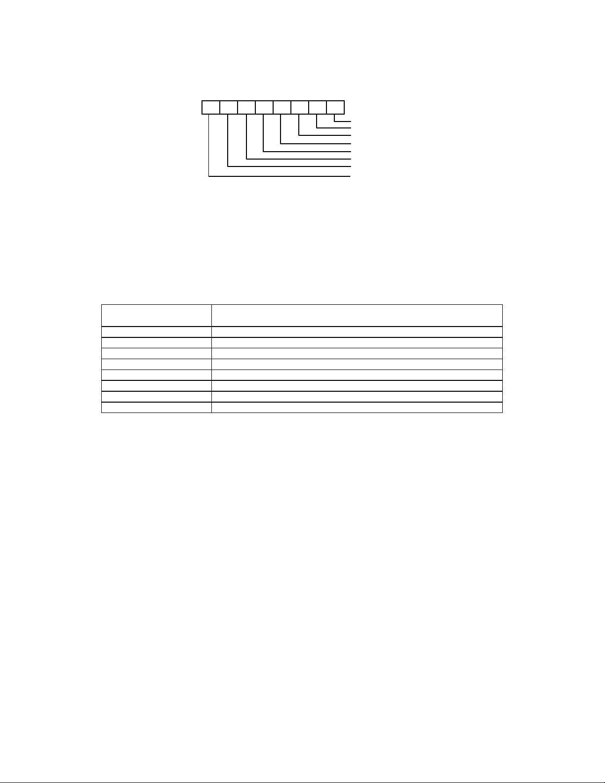
PWMOUT3/4 Clock Select -- Index 5Ch (
Bank 4
)
Register Location: 5Ch
Power on Default Value <7:0> 0001,0001. Reset by MR.
Attribute: Read/Write
Size: 8 bits
7 6 5 4 3 2 1 0
PWM3CLKSEL
PWM3CLKSEL
PWM3CLKSEL
Reserved
PWM4CLKSEL
PWM4CLKSEL
PWM4CLKSEL
Reserved
Bit 7: Reserved.
Bit 6-4: PWMOUT4 clock selection.
The clock frequency definition is same as PWMOUT3 clock selection.
Bit 3: Reserved.
Bit 2-0: PWMOUT3 clock Selection.
<2:0> = 000: 46.87KHz
<2:0> = 001: 23.43KHz (Default)
<2:0> = 010: 11.72KHz
<2:0> = 011: 5.85KHz
<2:0> = 100: 2.93KHz
Value RAM 2
ADDRESS A6-A0
AUTO-INCREMENT
Index 50h - 5Ah (auto-increment)
!!!!
50h
51h
5VSB reading
VBAT reading
(BANK 5)
DESCRIPTION
52h Reserved
53h Reserved
54h 5VSB High Limit
55h 5VSB Low Limit.
56h VBAT High Limit
57h VBAT Low Limit
SMSC Test Register - Index 50h (
Bank 6
)
53
Page 54
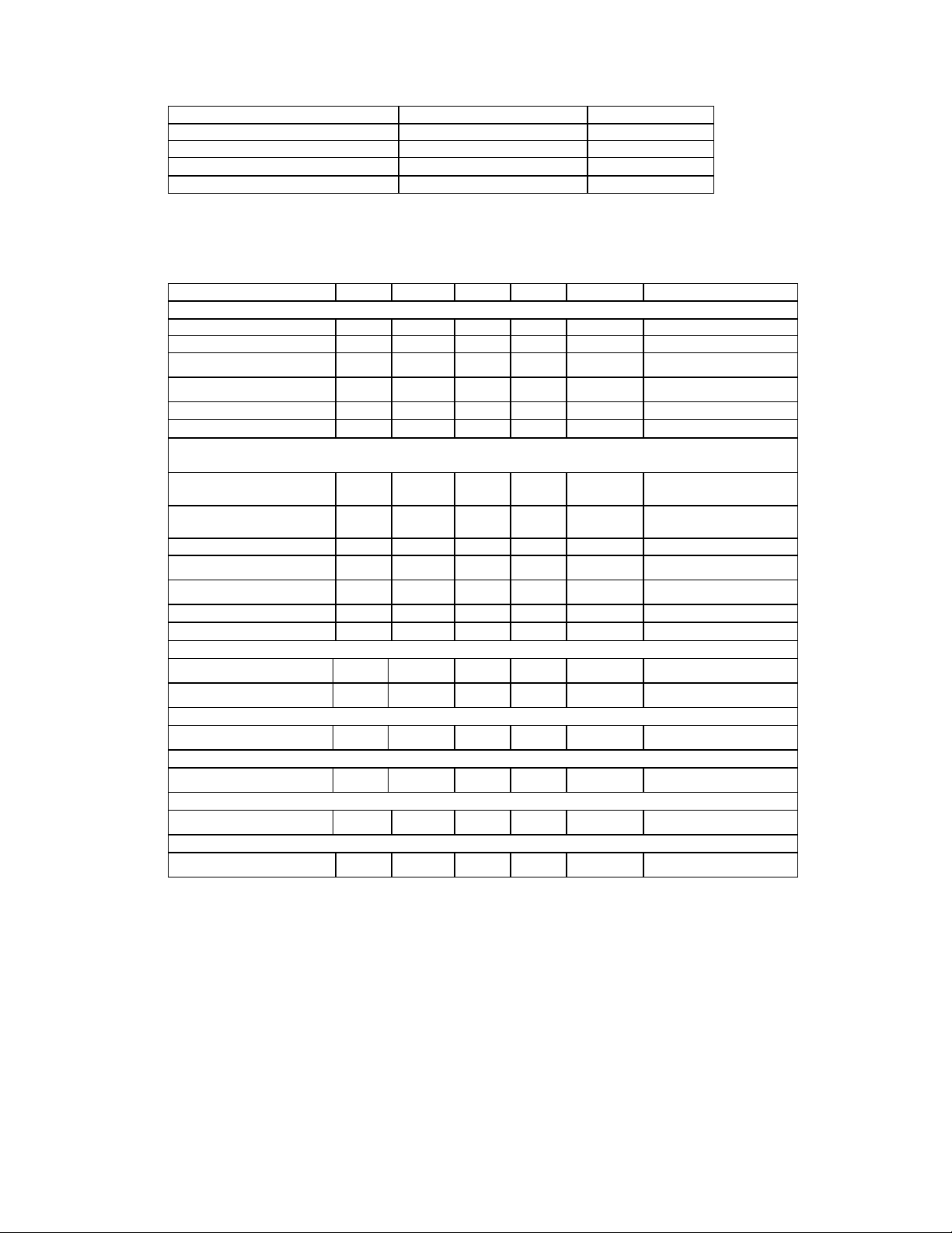
SPECIFICATIONS
Absolute Maximum Ratings
PARAMETER RATING UNIT
Power Supply Voltage -0.5 to 7.0 V
Input Voltage -0.5 to VDD+0.5 V
Operating Temperature 0 to +70
Storage Temperature -55 to +150
% C
% C
Note: Exposure to conditions beyond those listed under Absolute Maximum Ratings may adversely
affect the life and reliability of the device.
DC Characteristics
(Ta = 0% C to 70% C, VDD = 5V $ 10%, VSS = 0V)
PARAMETER SYM. MIN. TYP. MAX. UNIT CONDITIONS
I/O
- TTL level bi-directional pin with source-sink capability of 12 mA
12t
Input Low Voltage VIL 0.8 V
Input High Voltage VIH 2.0 V
Output Low Voltage VOL 0.4 V
Output High Voltage VOH 2.4 V
Input High Leakage ILIH +10
Input Low Leakage ILIL -10
I/O
- TTL level bi-directional pin with source-sink capability of 12 mA and schmitt-trigger
12ts
&A
&A
IOL = 12 mA
IOH = - 12 mA
VIN = VDD
VIN = 0V
level input
Input Low Threshold
Vt- 0.5 0.8 1.1 V VDD = 5 V
Voltage
Input High Threshold
Vt+ 1.6 2.0 2.4 V VDD = 5 V
Voltage
Hysteresis VTH 0.5 1.2 V VDD = 5 V
Output Low Voltage VOL 0.4 V
Output High Voltage VOH 2.4 V
Input High Leakage ILIH +10
Input Low Leakage ILIL -10
OUT
- TTL level output pin with source-sink capability of 12 mA
12t
&A
&A
Output Low Voltage VOL 0.4 V
Output High Voltage VOH 2.4 V
IOL = 12 mA
IOH = - 12 mA
VIN = VDD
VIN = 0V
IOL = 12 mA
IOH = -12 mA
OD8 - Open-drain output pin with sink capability of 8 mA
Output Low Voltage VOL 0.4 V
IOL = 8 mA
OD12 - Open-drain output pin with sink capability of 12 mA
Output Low Voltage VOL 0.4 V
IOL = 12 mA
OD48 - Open-drain output pin with sink capability of 48 mA
Output Low Voltage VOL 0.4 V
IOL = 48 mA
INt - TTL level input pin
Input Low Voltage VIL 0.8 V
54
Page 55

PARAMETER SYM. MIN. TYP. MAX. UNIT CONDITIONS
Input High Voltage VIH 2.0 V
Input High Leakage ILIH +10
Input Low Leakage ILIL -10
INts - TTL level Schmitt-triggered input pin
Input Low Threshold
Voltage
Input High Threshold
Voltage
Hysteresis VTH 0.5 1.2 V VDD = 5 V
Input High Leakage ILIH +10
Input Low Leakage ILIL -10
Vt- 0.5 0.8 1.1 V VDD = 5 V
Vt+ 1.6 2.0 2.4 V VDD = 5 V
&A
&A
&A
&A
VIN = VDD
VIN = 0 V
VIN = VDD
VIN = 0 V
55
Page 56
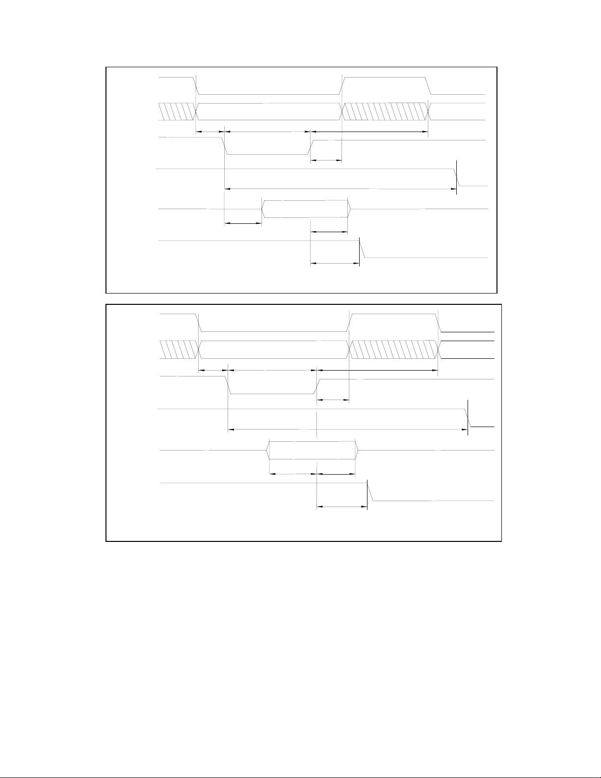
AC CHARACTERISTICS
g
g
ISA Read/Write Interface Timing
AEN
SA[2:0],nCS
t
AR
nIOR
nIOW
t
RD
t
RA
RC
t
RCU
SD[7:0]
IRQ
AEN
SA[2:0],nCS
nIOW
nIOR
SD[7:0]
IRQ
t
AW
t
RVD
VALID DATA
ISA Bus Read Timin
VALID
t
WR
VALID DATA
t
DS
t
RDH
t
RI
VALID
t
WCU
t
WA
WC
t
DH
t
WI
ISA Bus Write Timin
56
Page 57
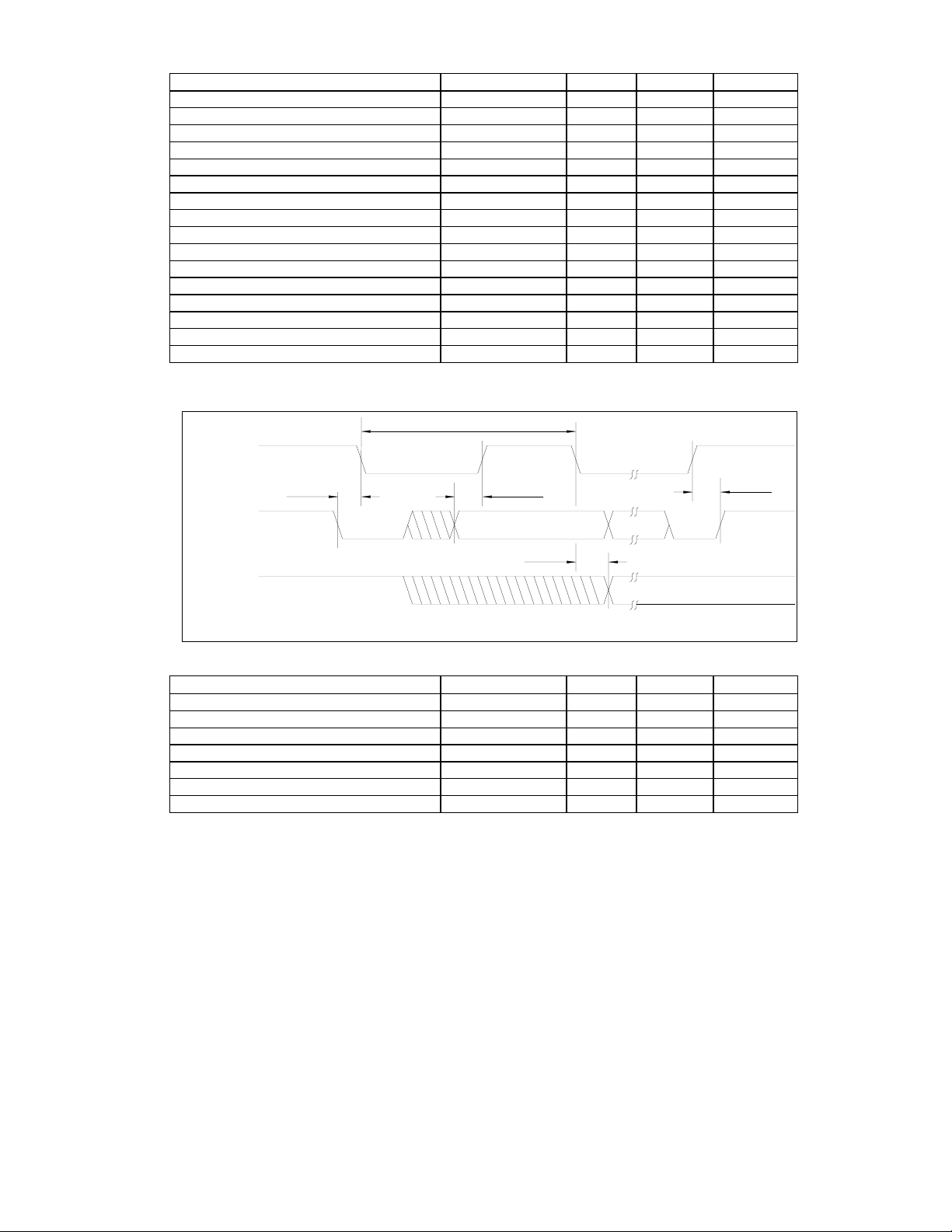
ISA Read/Write Timing
PARAMETER SYMBOL MIN. MAX. UNIT
Valid Address to Read Active t
-
10 nS
AR
Valid Address to Write Active tAW 10 nS
Data Hold tDH 5 nS
Data Setup tDS 80 nS
Address Hold from Inactive Read tRA 40 nS
Read Cycle Update t
200 nS
RCU
Read Strobe Width tRD 120 nS
Read Data Hold t
40 nS
RDH
Read Strobe to Clear IRQ tRI 60 nS
Active Read to Valid Data t
115 nS
RVD
Address Hold from Inactive Write tWA 5 nS
Write Cycle Update t
80 nS
WCU
Write Strobe to Clear IRQ tWI 60 nS
Write Strobe Width tWR 120 nS
Read Cycle = t
Write Cycle = tAW+tWR - t
AR
+ tRD+t
RC 210 nS
RCV
WC 210 nS
WCV
Serial Bus Timing Diagram
t
SCL
SCL
t
t
HD;SDA
t
HD;DAT
SU;STO
SDA IN
VALID DATA
t
SU;DAT
SDA OUT
Serial Bus Timing Diagram
Serial Bus Timing
PARAMETER SYMBOL MIN. MAX. UNIT
SCL clock period t
Start condition hold time t
Stop condition setup-up time t
DATA to SCL setup time t
DATA to SCL hold time t
-
10 uS
SCL
4.7 uS
HD;SDA
4.7 uS
SU;STO
120 nS
SU;DAT
5 nS
HD;DAT
SCL and SDA rise time tR 1.0 uS
SCL and SDA fall time tF 300 nS
57
Page 58
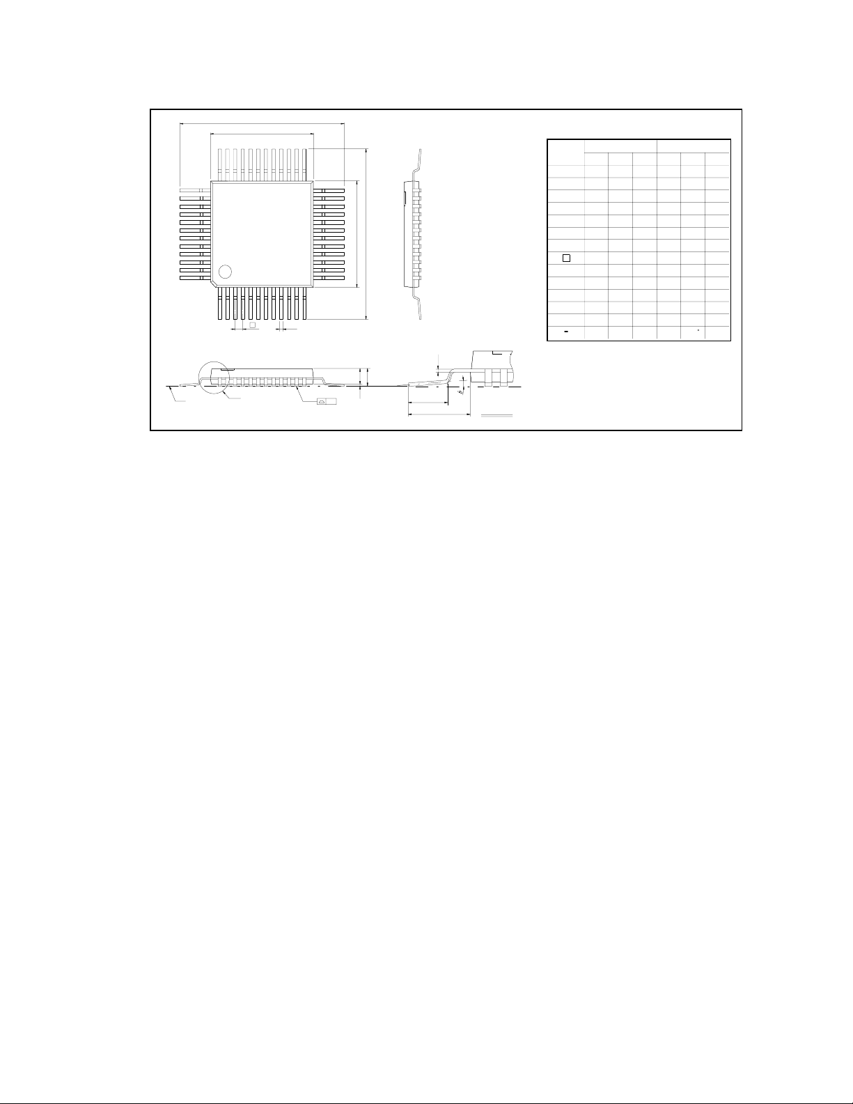
PACKAGE DIMENSIONS
p
(48 Pin TQFP)
D
e
See Detail F
H
D
25
12
b
36
37
48
1
Seating Plane
Dimension in inch Dimension in mm
Symbol
A
1
24
A
2
A
b
E
E
H
13
c
D
E
e
D
H
H
E
L
1
L
y
0
c
A
2
A
1
A
y
L
L
1
Detail F
Notes:
1. Dimensions D & E do not include interlead
flash.
2. Dimension b does not include dambar
protrusion/intrusion.
3. Controlling dimension: Millimeters
4. General appearance spec. should be based
on final visual ins
Min.
Nom.
Max. Max.
Min.
0.05
1.35
0.17 0.27
ection spec.
0.09
0.45
Nom.
1.40
0.20
7.00
7.00
0.50
9.00
9.00
1.00
0.60
0.08
1.60
---
0.15
---
1.45
---
0.20
0.75
--7
3.5
---
--0
58
Page 59

MON35W42 REVISIONS
PAGE(S) SECTION/FIGURE/ENTRY CORRECTION DATE REVISED
39 Diode Selection Register -- Index
59h (Bank 0)
41 VBAT Monitor Control Register --
Index 5Dh (
Bank 0
)
Added the content of Diode Selection
Register Index 59h (Bank 0 )
Modified VBAT Monitor Control Resgister
Index 5Dh (Bank 0 )
04/19/00
04/19/00
N/A Original Release -------------------------------------------------------- 01/12/99
Page 60

© STANDARD MICROSYSTEMS CORPORATION (SMSC) 2000
80 Arkay Drive
Hauppauge, NY 11788
(631) 435-6000
FAX (631) 273-3123
Standard Microsystems is a registered trademark of Standard Microsystems Corporation, and SMSC is a trademark of
Standard Microsystems Corporation. Penti um is a registered trademar k of Intel Corporation. Product names and company
names are the tradem arks of their respective holders. Ci rcuit diagrams utilizing S MSC products ar e included as a means of
illustrating typical applications; consequently complete information sufficient for construction purposes is not necessarily
given. Although the information has been checked and is believed to be accurate, no responsibility is assumed for
inaccuracies. SMSC reserves the right to make changes to specifications and product descriptions at any time without
notice. Contact your local SMSC sales office to obtain the latest specifications before placing your product order. The
provision of this information does not convey to the purchaser of the semiconductor devices described any licenses under
the patent rights of SMSC or others. All sales are expr essly conditional on your agreement to the terms and conditions of the
most recently dated version of SMSC's standard Terms of S ale Agreement dated befor e the date of your order (the "Terms of
Sale Agreement"). The product may contain design defects or error s known as anomalies which may cause the product's
functions to deviate from published specifications. Anomaly sheets are available upon request. SMSC products are not
designed, intended, authorized or warranted for use in any life support or other appli cation wher e pr oduct failur e coul d cause
or contribute to personal injury or severe property damage. Any and all such uses without prior written approval of an Officer
of SMSC and further testing and/or modification will be fully at the risk of the customer. Copies of this document or other
SMSC literature, as well as the Terms of Sale Agreement, may be obtained by visiting SMSC’s website at
http://www.smsc.com.
SMSC DISCLAIMS AND EXCLUDES ANY AND ALL WARRANTIES, INCLUDING WITHOUT LIMITATION ANY AND ALL IMPLIED
WARRANTIES OF MERCHANTABILITY, FITNESS FOR A PARTICULAR PURPOSE, TITLE, AND AGAINST INFRINGEMENT,
AND ANY AND ALL WA RRANTIES ARISING FROM ANY COURSE OF DEALING OR USAGE OF TRADE.
IN NO EVENT SHALL SMSC BE LIABLE FOR ANY DIRECT, INCIDENTAL, INDIRECT, SPECIAL, PUNITIVE, OR
CONSEQUENTIAL DAMAGES, OR FOR LOST DATA, PROFITS, SAVINGS OR REVENUES OF ANY KIND; REGARDLESS OF
THE FORM OF ACTION, WHETHER BASED ON CONTRACT, TORT, NEGLIGENCE OF SMSC OR OTHERS, STRICT LIABILITY,
BREACH OF WARRANTY, OR OTHERWISE; WHETHER OR NOT ANY REMEDY IS HELD TO HAVE FAILED OF ITS ESSENTIAL
PURPOSE; AND WHETHER OR NOT SMSC HAS BEEN ADVISED OF THE POSSIBILITY OF SUCH DAMAGES.
MON35W42 Rev. 04/19/2000
 Loading...