

Page 1
Ember EM358x
EMBER
This reference manual accompanies several documents to provide the complete description of Ember
devices. In the event that the device data sheet and this document contain conflicting information, the device data
sheet should be considered the authoritative source.
EM358X REFERENCE MANUAL
®
EM358x
®
Rev 0.4 8/13 Copyright © 2013 by Silicon Laboratories EM358x
This information applies to a product under development. Its characteristics and specifications are subject to change without notice.
Page 2

EM358x
2 Rev. 0.4
Page 3

EM358x
TABLE OF CONTENTS
1 Related Documents and Conventions ............................................................................... 8
1.1 Related Documents ........................................................................................................ 8
1.1.1 EM358x Data Sheet ............................................................................................ 8
1.1.2 ZigBee Specification ........................................................................................... 8
1.1.3 ZigBee PRO Stack Profile ................................................................................... 8
1.1.4 ZigBee Stack Profile ............................................................................................ 8
1.1.5 Bluetooth Core Specification ............................................................................... 8
1.1.6 IEEE 802.15.4-2003 ............................................................................................ 8
1.1.7 IEEE 802.11g ...................................................................................................... 8
1.1.8 USB 2.0 Specification ......................................................................................... 8
1.1.9 ARM® Cortex™-M3 Reference Manual ............................................................... 8
1.2 Conventions .................................................................................................................... 9
2 ARM® Cortex™-M3 and Memory Modules ....................................................................... 12
2.1 ARM® Cortex™-M3 Microprocessor ............................................................................. 12
2.2 Embedded Memory ...................................................................................................... 13
2.2.1 Flash Memory ................................................................................................... 14
2.2.2 RAM .................................................................................................................. 17
2.2.3 Registers ........................................................................................................... 17
2.3 Memory Protection Unit ................................................................................................ 18
3 Interrupt System ................................................................................................................ 19
3.1 Nested Vectored Interrupt Controller (NVIC) ................................................................ 19
3.2 Event Manager ............................................................................................................. 22
3.3 Non-maskable Interrupt (NMI) ...................................................................................... 24
3.4 Faults ............................................................................................................................ 25
3.5 Registers ....................................................................................................................... 26
4 Radio Module ..................................................................................................................... 33
4.1 Receive (Rx) Path ......................................................................................................... 33
4.1.1 Rx Baseband .................................................................................................... 33
4.1.2 RSSI and CCA .................................................................................................. 34
4.2 Transmit (Tx) Path ........................................................................................................ 34
4.2.1 Tx Baseband ..................................................................................................... 34
4.2.2 TX_ACTIVE and nTX_ACTIVE Signals ............................................................ 34
4.3 Calibration ..................................................................................................................... 34
4.4 Integrated MAC Module ................................................................................................ 34
4.5 Packet Trace Interface (PTI) ......................................................................................... 35
4.6 Random Number Generator ......................................................................................... 35
5 System Modules ................................................................................................................ 36
5.1 Power domains ............................................................................................................. 37
5.1.1 Internally regulated power ................................................................................. 37
5.1.2 Externally regulated power ................................................................................ 37
5.2 Resets ........................................................................................................................... 37
5.2.1 Reset Sources .................................................................................................. 37
5.2.2 Reset Recording ............................................................................................... 39
5.2.3 Reset Generation Module ................................................................................. 39
5.3 Clocks ........................................................................................................................... 40
Rev. 0.4 3
Page 4

EM358x
5.3.1 High-Frequency Internal RC Oscillator (OSCHF) .............................................. 42
5.3.2 High-Frequency Crystal Oscillator (OSC24M) .................................................. 42
5.3.3 Low-Frequency Internal RC Oscillator (OSCRC) .............................................. 43
5.3.4 Low-Frequency Crystal Oscillator (OSC32K) .................................................... 43
5.3.5 Clock Switching ................................................................................................. 44
5.4 System Timers .............................................................................................................. 44
5.4.1 Watchdog Timer ................................................................................................ 44
5.4.2 Sleep Timer ....................................................................................................... 45
5.4.3 Event Timer ....................................................................................................... 45
5.5 Power Management ...................................................................................................... 45
5.5.1 Wake Sources ................................................................................................... 45
5.5.2 Basic Sleep Modes ........................................................................................... 47
5.5.3 Further options for deep sleep .......................................................................... 47
5.5.4 RAM Retention in deep sleep ........................................................................... 48
5.5.5 Use of debugger with sleep modes ................................................................... 48
5.5.6 Registers ........................................................................................................... 49
5.6 Security Accelerator ...................................................................................................... 50
6 Integrated Voltage Regulator ........................................................................................... 51
7 GPIO (General Purpose Input / Output) ........................................................................... 52
7.1 GPIO Ports ................................................................................................................... 52
7.2 Configuration ................................................................................................................ 53
7.3 Forced Functions .......................................................................................................... 54
7.4 Reset ............................................................................................................................ 55
7.5 Boot Configuration ........................................................................................................ 55
7.6 GPIO Modes ................................................................................................................. 56
7.6.1 Analog Mode ..................................................................................................... 56
7.6.2 Input Mode ........................................................................................................ 56
7.6.3 SWDIO Mode .................................................................................................... 57
7.6.4 Output Mode ..................................................................................................... 57
7.6.5 Alternate Output Mode ...................................................................................... 57
7.6.6 Alternate Output SPI Slave MISO Mode ........................................................... 57
7.7 Wake Monitoring ........................................................................................................... 58
7.8 External Interrupts ........................................................................................................ 58
7.9 Debug Control and Status ............................................................................................. 59
7.10 GPIO Signal Assignment Summary ............................................................................ 59
7.11 Registers .................................................................................................................... 61
8 Serial Controllers .............................................................................................................. 74
8.1 Overview ....................................................................................................................... 74
8.2 Configuration ................................................................................................................ 75
8.2.1 Registers ........................................................................................................... 76
8.3 SPI - Master Mode ........................................................................................................ 80
8.3.1 GPIO Usage ...................................................................................................... 80
8.3.2 Set Up and Configuration .................................................................................. 80
8.3.3 Operation .......................................................................................................... 81
8.3.4 Interrupts ........................................................................................................... 82
8.3.5 Registers ........................................................................................................... 83
4 Rev. 0.4
Page 5

EM358x
8.4 SPI - Slave Mode .......................................................................................................... 88
8.4.1 GPIO Usage ...................................................................................................... 88
8.4.2 Set Up and Configuration .................................................................................. 88
8.4.3 Operation .......................................................................................................... 89
8.4.4 DMA .................................................................................................................. 90
8.4.5 Interrupts ........................................................................................................... 90
8.4.6 Registers ........................................................................................................... 90
8.5 TWI - Two Wire serial Interfaces ................................................................................... 90
8.5.1 GPIO Usage ...................................................................................................... 91
8.5.2 Set Up and Configuration .................................................................................. 91
8.5.3 Constructing Frames ......................................................................................... 91
8.5.4 Interrupts ........................................................................................................... 93
8.5.5 Registers ........................................................................................................... 94
8.6 UART - Universal Asynchronous Receiver / Transmitter .............................................. 97
8.6.1 GPIO Usage ...................................................................................................... 97
8.6.2 Set Up and Configuration .................................................................................. 97
8.6.3 FIFOs ................................................................................................................ 99
8.6.4 RTS/CTS Flow control ...................................................................................... 99
8.6.5 DMA ................................................................................................................ 100
8.6.6 Interrupts ......................................................................................................... 100
8.6.7 Registers ......................................................................................................... 102
8.7 DMA Channels ............................................................................................................ 106
8.7.1 Registers ......................................................................................................... 107
9 USB Device ...................................................................................................................... 124
9.1 Overview ..................................................................................................................... 124
9.2 Host Drivers ................................................................................................................ 124
9.3 References ................................................................................................................. 124
9.4 GPIO Usage and USB Pin Assignments..................................................................... 124
9.5 Application Schematics ............................................................................................... 125
9.6 Endpoints .................................................................................................................... 125
9.7 Buffers and DMA ........................................................................................................ 126
9.8 Set Up and Configuration ............................................................................................ 126
9.9 DMA Usage and Transfers ......................................................................................... 128
9.10 Enumeration ............................................................................................................. 128
9.11 Normal COM Port Operation .................................................................................... 128
9.12 Suspend and Resume .............................................................................................. 128
9.13 Interrupts .................................................................................................................. 128
9.13.1 Registers ......................................................................................................... 129
10 General Purpose Timers (TIM1 and TIM2) ..................................................................... 139
10.1 Introduction ............................................................................................................... 139
10.2 GPIO Usage ............................................................................................................. 140
10.3 Timer Functional Description .................................................................................... 141
10.3.1 Time-Base Unit ............................................................................................... 141
10.3.2 Counter Modes ............................................................................................... 142
10.3.3 Clock Selection ............................................................................................... 147
10.3.4 Capture/Compare Channels ........................................................................... 150
Rev. 0.4 5
Page 6

EM358x
10.3.5 Input Capture Mode ........................................................................................ 151
10.3.6 PWM Input Mode ............................................................................................ 152
10.3.7 Forced Output Mode ....................................................................................... 152
10.3.8 Output Compare Mode .................................................................................... 153
10.3.9 PWM Mode ..................................................................................................... 154
10.3.10One-Pulse Mode ............................................................................................ 156
10.3.11Encoder Interface Mode ................................................................................. 158
10.3.12Timer Input XOR Function ............................................................................. 159
10.3.13Timers and External Trigger Synchronization ................................................ 160
10.3.14Slave Mode: Reset Mode ............................................................................... 160
10.3.15Timer Synchronization ................................................................................... 162
10.3.16Timer Signal Descriptions .............................................................................. 166
10.4 Interrupts .................................................................................................................. 167
10.5 Registers .................................................................................................................. 168
11 ADC (Analog to Digital Converter) ................................................................................. 195
11.1 Setup and Configuration ........................................................................................... 195
11.1.1 GPIO Usage .................................................................................................... 196
11.1.2 Voltage Reference .......................................................................................... 196
11.1.3 Offset/Gain Correction .................................................................................... 196
11.1.4 DMA ................................................................................................................ 196
11.1.5 ADC Configuration Register ............................................................................ 197
11.2 Interrupts .................................................................................................................. 199
11.3 Operation .................................................................................................................. 200
11.4 Calibration ................................................................................................................ 200
11.5 ADC Key Parameters ............................................................................................... 201
11.6 Registers .................................................................................................................. 206
12 Trace Port Interface Unit (TPIU) ..................................................................................... 218
13 Instrumentation Trace Macrocell (ITM) .......................................................................... 219
14 Embedded Trace Macrocell (ETM) ................................................................................. 220
15 Data Watchpoint and Trace (DWT) ................................................................................. 221
16 Flash Patch and Breakpoint (FPB) ................................................................................. 222
17 Serial Wire and JTAG (SWJ) Interface ........................................................................... 223
A. Register Address Table .................................................................................................. 224
6 Rev. 0.4
Page 7

EM358x
Rev. 0.4 7
Page 8

EM358x
1 Related Documents and Conventions
1.1 Related Documents
This reference manual accompanies several documents to provide the complete description of the Ember
EM358x devices.
1.1.1 EM358x Data Sheet
The Silicon Laboratories EM358x data sheet provides the configuration information for the EM358x.
1.1.2 ZigBee Specification
The core ZigBee specification (Document 053474) defines ZigBee's smart, cost-effective and energy-efficient
mesh network. It can be downloaded from the ZigBee website (111.zigbee.org). ZigBee Alliance membership is
required.
1.1.3 ZigBee PRO Stack Profile
The ZigBee PRO Stack Profile specification (Document 074855) is optimized for low power consumption and to
support large networks with thousands of devices. It can be downloaded from the ZigBee website
(111.zigbee.org). ZigBee Alliance membership is required.
1.1.4 ZigBee Stack Profile
The ZigBee Stack Profile specification (Document 064321) is designed to support smaller networks with hundreds
of devices in a single network. It can be downloaded from the ZigBee website (111.zigbee.org). ZigBee Alliance
membership is required.
1.1.5 Bluetooth Core Specification
The Bluetooth specification is the global short-range wireless standard enabling connectivity for a broad range of
electronic devices. Version 2.1 + EDR (Enhanced Data Rate) can be found here:
http://www.bluetooth.org/docman/handlers/downloaddoc.ashx?doc_id=241363
1.1.6 IEEE 802.15.4-2003
This standard defines the protocol and compatible interconnection for data communication devices using low data
rate, low power and low complexity, short-range radio frequency (RF) transmissions in a wireless personal area
network (WPAN). It can be found here:
IEEE 802.15.4-2003 (http://standards.ieee.org/getieee802/download/802.15.4-2003.pdf)
1.1.7 IEEE 802.11g
This version provides changes and additions to support the further higher data rate extension for operation in the
2.4 GHz band. It can be found here:
standards.ieee.org/getieee802/download/802.11g-2003.pdf
1.1.8 USB 2.0 Specification
The Universal Serial Bus Revision 2.0 specification provides the technical details to understand USB
requirements and design USB compatible products. The main specification (usb_20.pdf) is part of the zipfile found
here:
http://www.usb.org/developers/docs/usb_20_101111.zip
®
1.1.9 ARM
ARM-specific features like the Nested Vector Interrupt Controller are described in the ARM
reference documentation. The online reference manual can be found here:
http://infocenter.arm.com/help/topic/com.arm.doc.subset.cortexm.m3/index.html#cortexm3
Cortex™-M3 Reference Manual
®
Cortex™-M3
8 Rev. 0.4
Page 9

1.2 Conventions
Abbreviations and acronyms used in this data sheet are explained in Table 1-1.
Table 1-1. Acronyms and Abbreviations
Acronym/Abbreviation Meaning
ACK Acknowledgement
ADC Analog to Digital Converter
AES Advanced Encryption Standard
AGC Automatic Gain Control
AHB Advanced High Speed Bus
APB Advanced Peripheral Bus
CBC-MAC Cipher Block Chaining—Message Authentication Code
CCA Clear Channel Assessment
CCM Counter with CBC-MAC Mode for AES encryption
CCM* Improved Counter with CBC-MAC Mode for AES encryption
EM358x
CIB Customer Information Block
CLK1K 1 kHz Clock
CLK32K 32.768 kHz Crystal Clock
CPU Central Processing Unit
CRC Cyclic Redundancy Check
CSMA-CA Carrier Sense Multiple Access-Collision Avoidance
CTR Counter Mode
CTS Clear to Send
DNL Differential Non-Linearity
DMA Direct Memory Access
DWT Data Watchpoint and Trace
EEPROM Electrically Erasable Programmable Read Only Memory
EM Event Manager
ENOB effective number of bits
ESD Electro Static Discharge
ESR Equivalent Series Resistance
ETR External Trigger Input
FCLK ARM® CortexTM-M3 CPU Clock
FIB Fixed Information Block
FIFO First-in, First-out
Rev. 0.4 9
Page 10

EM358x
Acronym/Abbreviation Meaning
FPB Flash Patch and Breakpoint
GPIO General Purpose I/O (pins)
HF High Frequency
I2C Inter-Integrated Circuit
IDE Integrated Development Environment
IF Intermediate Frequency
IEEE Institute of Electrical and Electronics Engineers
INL Integral Non-linearity
ITM Instrumentation Trace Macrocell
JTAG Joint Test Action Group
LF Low Frequency
LNA Low Noise Amplifier
LQI Link Quality Indicator
LSB Least significant bit
MAC Medium Access Control
MFB Main Flash Block
MISO Master in, slave out
MOS Metal Oxide Semiconductor (P-channel or N-channel)
MOSI Master out, slave in
MPU Memory Protection Unit
MSB Most significant bit
MSL Moisture Sensitivity Level
NACK Negative Acknowledge
NIST National Institute of Standards and Technology
NMI Non-Maskable Interrupt
NVIC Nested Vectored Interrupt Controller
OPM One-Pulse Mode
O-QPSK Offset-Quadrature Phase Shift Keying
OSC24M High Frequency Crystal Oscillator
OSC32K Low-Frequency 32.768 kHz Oscillator
OSCHF High-Frequency Internal RC Oscillator
OSCRC Low-Frequency RC Oscillator
PA Power Amplifier
10 Rev. 0.4
Page 11

Acronym/Abbreviation Meaning
PCLK Peripheral clock
PER Packet Error Rate
PHY Physical Layer
PLL Phase-Locked Loop
POR Power-On-Reset
PRNG Pseudo Random Number Generator
PSD Power Spectral Density
PTI Packet Trace Interface
PWM Pulse Width Modulation
QFN Quad Flat Pack
RAM Random Access Memory
RC Resistive/Capacitive
RF Radio Frequency
EM358x
RMS Root Mean Square
RoHS Restriction of Hazardous Substances
RSSI Receive Signal Strength Indicator
RTS Request to Send
Rx Receive
SYSCLK System clock
SDFR Spurious Free Dynamic Range
SFD Start Frame Delimiter
SINAD Signal-to-noise and distortion ratio
SPI Serial Peripheral Interface
SWJ Serial Wire and JTAG Interface
THD Total Harmonic Distortion
TRNG True random number generator
TWI Two Wire serial interface
Tx Transmit
UART Universal Asynchronous Receiver/Transmitter
UEV Update event
USB Universal Serial Bus
VCO Voltage Controlled Oscillator
Rev. 0.4 11
Page 12

EM358x
2 ARM® Cortex™-M3 and Memory Modules
This chapter discusses the ARM® CortexTM-M3 Microprocessor, and reviews the EM358x’s flash and RAM
memory modules as well as the Memory Protection Unit (MPU).
2.1 ARM® Cortex™-M3 Microprocessor
The EM358x integrates the ARM® CortexTM-M3 microprocessor, revision r1p1, developed by ARM Ltd., making
the EM358x a true System-on-Chip solution. The ARM
architecture processor that has separate internal program and data buses, but presents a unified program and
data address space to software. The word width is 32 bits for both the program and data sides. The ARM
TM
Cortex
The ARM
-M3 allows unaligned word and half-word data accesses to support efficiently-packed data structures.
®
CortexTM-M3 clock speed is configurable to 6 MHz, 12 MHz, or 24 MHz. For normal operation 24 MHz
is preferred over 12 MHz due to improved performance for all applications and improved duty cycling for
applications using sleep modes. The 6 MHz operation can only be used when radio operations are not required
since the radio requires an accurate 12 MHz clock.
®
The ARM
CortexTM-M3 in the EM358x has also been enhanced to support two separate memory protection
levels. Basic protection is available without using the MPU, but normal operation uses the MPU. The MPU allows
for protecting unimplemented areas of the memory map to prevent common software bugs from interfering with
software operation. The architecture could also allow for separation of the networking stack from the application
code using a fine granularity RAM protection module. Errant writes are captured and details are reported to the
developer to assist in tracking down and fixing issues.
®
CortexTM-M3 is an advanced 32-bit modified Harvard
®
12 Rev. 0.4
Page 13
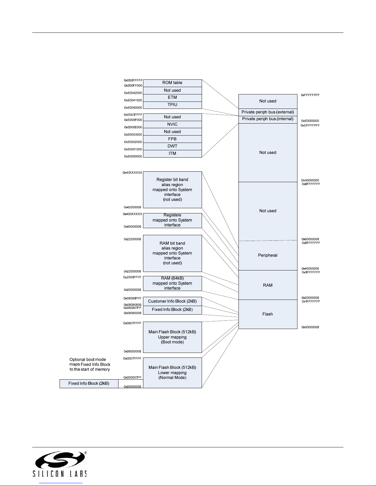
2.2 Embedded Memory
Figure 2-1 shows the EM358x ARM® CortexTM-M3 memory map.
EM358x
Figure 2-1. EM358x ARM® CortexTM-M3 Memory Map
Rev. 0.4 13
Page 14

EM358x
2.2.1 Flash Memory
2.2.1.1 Flash Overview
The EM358x provides a total of either 256 or 512 kB of flash memory. The flash memory is provided in three
separate blocks:
Main Flash Block (MFB)
Fixed Information Block (FIB)
Customer Information Block (CIB)
The MFB is divided into 2048-byte pages. The EM358x has either 128 or 256 pages. The CIB is a single 2048byte page. The FIB is a single 2048-byte page. The smallest erasable unit is one page and the smallest writable
unit is an aligned 16-bit half-word. The flash is rated to have a guaranteed 20,000 write/erase cycles. The flash
cell has been qualified for a data retention time of >100 years at room temperature.
Flash may be programmed either through the Serial Wire/JTAG interface or through bootloader software.
Programming flash through Serial Wire/JTAG requires the assistance of RAM-based utility code. Programming
through a bootloader requires Ember software for over-the-air loading or serial link loading.
2.2.1.2 Main Flash Block
The start of the MFB is mapped to both address 0x00000000 and address 0x08000000 in normal boot mode, but
is mapped only to address 0x08000000 in FIB monitor mode (see also section 7.5, Boot Configuration in Chapter
7, GPIO). Consequently, it is recommended that software intended to execute from the MFB is designed to
operate from the upper address, 0x08000000, since this address mapping is always available in all modes.
The MFB stores all program instructions and constant data. A small portion of the MFB is devoted to non-volatile
token storage using the Ember Simulated EEPROM system.
2.2.1.3 Fixed Information Block
The 2 kB FIB is used to store fixed manufacturing data including serial numbers and calibration values. The start
of the FIB is mapped to address 0x08080000. This block can only be programmed during production by Silicon
Labs.
The FIB also contains a monitor program, which is a serial-link-only way of performing low-level memory access.
In FIB monitor mode (see section 7.5, Boot Configuration in Chapter 7, GPIO), the start of the FIB is mapped to
both address 0x00000000 and address 0x08080000 so the monitor may be executed out of reset.
2.2.1.4 Customer Information Block
The 2048 byte CIB can be used to store customer data. The start of the CIB is mapped to address 0x08080800.
The CIB cannot be executed.
The first eight half-words of the CIB are dedicated to special storage called option bytes. An option byte is a 16 bit
quantity of flash where the lower 8 bits contain the data and the upper 8 contain the inverse of the lower 8 bits.
The upper 8 bits are automatically generated by hardware and cannot be written to by the user, see Table 2-1.
The option byte hardware also verifies the inverse of each option byte when exiting from reset and generates an
error, which prevents the CPU from executing code, if a discrepancy is found. All of this is transparent to the user.
14 Rev. 0.4
Page 15

EM358x
Table 2-1. Option Byte Storage
Address bits [15:8] bits [7:0] Notes
0x08080800 Inverse Option Byte 0 Option Byte 0 Configures flash read protection
0x08080802 Inverse Option Byte 1 Option Byte 1 Reserved
0x08080804 Inverse Option Byte 2 Option Byte 2 Available for customer use1
0x08080806 Inverse Option Byte 3 Option Byte 3 Available for customer use1
0x08080808 Inverse Option Byte 4 Option Byte 4 Configures flash write protection
0x0808080A Inverse Option Byte 5 Option byte 5 Configures flash write protection
0x0808080C Inverse Option Byte 6 Option Byte 6 Configures flash write protection
0x0808080E Inverse Option Byte 7 Option Byte 7 Configures flash write protection
1
Option bytes 2 and 3 do not link to any specific hardware functionality other than the option byte loader. Therefore, they are best used
for storing data that requires a hardware verification of the data integrity.
Table 2-2 shows the mapping of the option bytes that are used for read and write protection of the flash. Each bit
of the flash write protection option bytes protects a 4 page region of the main flash block. The EM358x has up to
32 regions and therefore option bytes 4, 5, 6, and 7 control flash write protection. These write protection bits are
active low, and therefore the erased state of 0xFF disables write protection. Like read protection, write protection
only takes effect after a reset. Write protection not only prevents a write to the region, but also prevents page
erasure.
Option byte 0 controls flash read protection. When option byte 0 is set to 0xA5, read protection is disabled. All
other values, including the erased state 0xFF, enable read protection when coming out of reset. The internal state
of read protection (active versus disabled) can only be changed by applying a full chip reset. If a debugger is
connected to the EM358x, the intrusion state is latched. Read protection is combined with this latched intrusion
signal. When both read protection and intrusion are set, all flash is disconnected from the internal bus. As a side
effect, the CPU cannot execute code since all flash is disconnected from the bus. This functionality prevents a
debug tool from being able to read the contents of any flash. The only means of clearing the intrusion signal is to
disconnect the debugger and reset the entire chip using the nRESET pin. By requiring a chip reset, a debugger
cannot install or execute malicious code that could allow the contents of the flash to be read.
The only way to disable read protection is to program option byte 0 with the value 0xA5. Option byte 0 must be
erased before it can be programmed. Erasing option byte 0 while read protection is active automatically masserases the main flash block. By automatically erasing main flash, a debugger cannot disable read protection and
readout the contents of main flash without destroying its contents.
In general, if read protection is active then write protection should also be active. This prevents an attacker from
reprogramming flash with malicious code that could readout the flash after the debugger is disconnected. To
obtain fully protected flash, both read protection and write protection should be active.
Table 2-2. Option Byte Write Protection Bit Map
Option Byte Bit Notes
Option Byte 0 bit [7:0] Read protection of all flash (MFB, FIB, CIB)
Option Byte 1 bit [7:0] Reserved for Silicon Labs use
Option Byte 2 bit [7:0] Available for customer use
Option Byte 3 bit [7:0] Available for customer use
Rev. 0.4 15
Page 16

EM358x
Option Byte Bit Notes
Option Byte 4 bit [0] Write protection of address range 0x08000000 – 0x08003FFF
bit [1] Write protection of address range 0x08004000 – 0x08007FFF
bit [2] Write protection of address range 0x08008000 – 0x0800BFFF
bit [3] Write protection of address range 0x0800C000 – 0x0800FFFF
bit [4] Write protection of address range 0x08010000 – 0x08013FFF
bit [5] Write protection of address range 0x08014000 – 0x08017FFF
bit [6] Write protection of address range 0x08018000 – 0x08013FFF
bit [7] Write protection of address range 0x0801C000 – 0x0801FFFF
Option Byte 5 bit [0] Write protection of address range 0x08020000 – 0x08023FFF
bit [1] Write protection of address range 0x08024000 – 0x08027FFF
bit [2] Write protection of address range 0x08028000 – 0x0802BFFF
bit [3] Write protection of address range 0x0802C000 – 0x0802FFFF
bit [4] Write protection of address range 0x08030000 – 0x08033FFF
bit [5] Write protection of address range 0x08034000 – 0x08037FFF
bit [6] Write protection of address range 0x08038000 – 0x0803BFFF
bit [7] Write protection of address range 0x0803C000 – 0x0803FFFF
Option Byte 6 bit [0] Write protection of address range 0x08040000 – 0x08043FFF
bit [1] Write protection of address range 0x08044000 – 0x08047FFF
bit [2] Write protection of address range 0x08048000 – 0x0804BFFF
bit [3] Write protection of address range 0x0804C000 – 0x0804FFFF
bit [4] Write protection of address range 0x08050000 – 0x08053FFF
bit [5] Write protection of address range 0x08054000 – 0x08057FFF
bit [6] Write protection of address range 0x08058000 – 0x0805BFFF
bit [7] Write protection of address range 0x0805C000 – 0x0805FFFF
Option Byte 7 bit [0] Write protection of address range 0x08060000 – 0x08063FFF
bit [1] Write protection of address range 0x08064000 – 0x08067FFF
bit [2] Write protection of address range 0x08068000 – 0x0806BFFF
bit [3] Write protection of address range 0x0806C000 – 0x0806FFFF
bit [4] Write protection of address range 0x08070000 – 0x08073FFF
bit [5] Write protection of address range 0x08074000 – 0x08077FFF
bit [6] Write protection of address range 0x08078000 – 0x0807BFFF
bit [7] Write protection of address range 0x0807C000 – 0x0807FFFF
16 Rev. 0.4
Page 17

EM358x
2.2.1.5 Simulated EEPROM
Ember software reserves 8 kB of the main flash block as a simulated EEPROM storage area for stack and
customer tokens. The simulated EEPROM storage area implements a wear-leveling algorithm to extend the
number of simulated EEPROM write cycles beyond the physical limit of 20,000 write cycles for which each flash
cell is qualified.
2.2.2 RAM
2.2.2.1 RAM Overview
The EM358x has either 32 or 64 kB of static RAM on-chip. The start of RAM is mapped to address 0x20000000.
Although the ARM
does not permit use of the bit-band feature.
The RAM is physically connected to the AHB System bus and is therefore accessible to both the ARM
M3 microprocessor and the debugger. The RAM can be accessed for both instruction and data fetches as bytes,
half words, or words. The standard MPU configuration does not permit execution from the RAM, but for special
purposes the MPU may be disabled. To the bus, the RAM appears as 32-bit wide memory and in most situations
has zero wait state read or write access. In the higher CPU clock mode the RAM requires one wait state. This is
handled by hardware transparent to the user application with no configuration required.
2.2.2.2 Direct Memory Access (DMA) to RAM
Several of the peripherals are equipped with DMA controllers allowing them to transfer data into and out of RAM
autonomously. This applies to the radio (802.15.4-2003 MAC), general purpose ADC, USB device controller and
the two serial controllers. In the case of the serial controllers, the DMA is full duplex so that a read and a write to
RAM may be requested at the same time. Thus there are six DMA channels in total. See Chapter 8, Section 8.7
and Chapter 11, Section 11.1.4 for a description of how to configure the serial controllers and ADC for DMA
operation. The DMA channels do not use AHB system bus bandwidth as they access the RAM directly.
The EM358x integrates a DMA arbiter that ensures fair access to the microprocessor as well as the peripherals
through a fixed priority scheme appropriate to the memory bandwidth requirements of each master. The priority
scheme is as follows, with the top peripheral being the highest priority:
1. USB Device Controller (where applicable)
2. General Purpose ADC
3. Serial Controller 2 Receive
4. Serial Controller 2 Transmit
5. MAC
6. Serial Controller 1 Receive
7. Serial Controller 1 Transmit
®
CortexTM-M3 allows bit band accesses to this address region, the standard MPU configuration
®
CortexTM-
2.2.2.3 RAM Memory Protection
The EM358x integrates a memory protection mechanism through the ARM® CortexTM-M3 Memory Protection Unit
(MPU) described in the Memory Protection Unit section. The MPU may be used to protect any area of memory.
MPU configuration is normally handled by Ember software.
2.2.3 Registers
Appendix A, Register Address Table provides a short description of all application-accessible registers within the
EM358. Complete descriptions are provided at the end of each applicable peripheral’s description. The registers
are mapped to the system address space starting at address 0x40000000. These registers allow for the control
and configuration of the various peripherals and modules. The CPU only performs word-aligned accesses on the
system bus. The CPU performs a word aligned read-modify-write for all byte, half-word, and unaligned writes and
a word-aligned read for all reads. Silicon Labs recommends accessing all peripheral registers using word-aligned
addressing.
As with the RAM, the peripheral registers fall within an address range that allows for bit-band access by the ARM
TM
Cortex
Rev. 0.4 17
-M3, but the standard MPU configuration does not allow access to this alias address range.
®
Page 18

EM358x
2.3 Memory Protection Unit
The EM358x includes the ARM® CortexTM-M3 Memory Protection Unit, or MPU. The MPU controls access rights
and characteristics of up to eight address regions, each of which may be divided into eight equal sub-regions.
Refer to the ARM
Ember software configures the MPU in a standard configuration and application software should not modify it. The
configuration is designed for optimal detection of illegal instruction or data accesses. If an illegal access is
attempted, the MPU captures information about the access type, the address being accessed, and the location of
the offending software. This simplifies software debugging and increases the reliability of deployed devices. As a
consequence of this MPU configuration, accessing RAM and register bit-band address alias regions is not
permitted, and generates a bus fault if attempted.
®
CortexTM-M3 Technical Reference Manual (DDI 0337A) for a detailed description of the MPU.
18 Rev. 0.4
Page 19

EM358x
3 Interrupt System
The EM358x’s interrupt system is composed of two parts: a standard ARM® CortexTM-M3 Nested Vectored
Interrupt Controller (NVIC) that provides top-level interrupts, and a proprietary Event Manager (EM) that provides
second-level interrupts. The NVIC and EM provide a simple hierarchy. All second-level interrupts from the EM
feed into top-level interrupts in the NVIC. This two-level hierarchy allows for both fine granular control of interrupt
sources and coarse granular control over entire peripherals, while allowing peripherals to have their own interrupt
vector.
The Nested Vectored Interrupt Controller (NVIC) section provides a description of the NVIC and an overview of
the exception table (ARM nomenclature refers to interrupts as exceptions). The Event Manager section provides a
more detailed description of the Event Manager including a table of all top-level peripheral interrupts and their
second-level interrupt sources.
In practice, top-level peripheral interrupts are only used to enable or disable interrupts for an entire peripheral.
Second-level interrupts originate from hardware sources, and therefore are the main focus of applications using
interrupts.
3.1 Nested Vectored Interrupt Controller (NVIC)
The ARM® CortexTM-M3 Nested Vectored Interrupt Controller (NVIC) facilitates low-latency exception and
interrupt handling. The NVIC and the processor core interface are closely coupled, which enables low-latency
interrupt processing and efficient processing of late-arriving interrupts. The NVIC also maintains knowledge of the
stacked (nested) interrupts to enable tail-chaining of interrupts.
®
The ARM
management. In addition to the 10 standard interrupts, it contains 18 individually vectored peripheral interrupts
specific to the EM358x.
The NVIC defines a list of exceptions. These exceptions include not only traditional peripheral interrupts, but also
more specialized events such as faults and CPU reset. In the ARM
considered an exception of the highest priority, and the stack pointer is loaded from the first position in the NVIC
exception table. The NVIC exception table defines all exceptions and their position, including peripheral interrupts.
The position of each exception is important since it directly translates to the location of a 32-bit interrupt vector for
each interrupt, and defines the hardware priority of exceptions. Each exception in the table is a 32-bit address that
is loaded into the program counter when that exception occurs. Table 3-1 lists the entire exception table.
Exceptions 0 (stack pointer) through 15 (SysTick) are part of the standard ARM
exceptions 16 (Timer 1) through 35 (USB, where applicable) are the peripheral interrupts specific to the EM358x
peripherals. The peripheral interrupts are listed in greater detail in Table 3-2.
CortexTM-M3 NVIC contains 10 standard interrupts that are related to chip and CPU operation and
®
CortexTM-M3 NVIC, a CPU reset event is
®
CortexTM-M3 NVIC, while
Table 3-1. NVIC Exception Table
Exception Position Description
-
Reset
NMI
Hard Fault
Memory Fault
Bus Fault
Usage Fault
-
Rev. 0.4 19
0
1
2
3
4
5
6
7-10
Stack top is loaded from first entry of vector table on reset.
Invoked on power up and warm reset. On first instruction, drops to lowest
priority (Thread mode). Asynchronous.
Cannot be stopped or preempted by any exception but reset. Asynchronous.
All classes of fault, when the fault cannot activate because of priority or the
Configurable Fault handler has been disabled. Synchronous.
MPU mismatch, including access violation and no match. Synchronous.
Pre-fetch, memory access, and other address/memory-related faults.
Synchronous when precise and asynchronous when imprecise.
Usage fault, such as ‘undefined instruction executed’ or ‘illegal state transition
attempt’. Synchronous.
Reserved.
Page 20

EM358x
Exception Position Description
SVCall
Debug Monitor
-
PendSV
SysTick
Timer 1
Timer 2
Management
Baseband
Sleep Timer
Serial Controller 1
Serial Controller 2
Security
MAC Timer
MAC Transmit
MAC Receive
ADC
IRQA
IRQB
IRQC
IRQD
Debug
-
-
USB
11
12
13
14
15
16
17
18
19
20
21
22
23
24
25
26
27
28
29
30
31
32
33
34
35
System service call with SVC instruction. Synchronous.
Debug monitor, when not halting. Synchronous, but only active when enabled. It
does not activate if lower priority than the current activation.
Reserved.
Pendable request for system service. Asynchronous and only pended by software.
System tick timer has fired. Asynchronous.
Timer 1 peripheral interrupt.
Timer 2 peripheral interrupt.
Management peripheral interrupt.
Baseband peripheral interrupt.
Sleep Timer peripheral interrupt.
Serial Controller 1 peripheral interrupt.
Serial Controller 2 peripheral interrupt.
Security peripheral interrupt.
MAC Timer peripheral interrupt.
MAC Transmit peripheral interrupt.
MAC Receive peripheral interrupt.
ADC peripheral interrupt.
IRQA peripheral interrupt.
IRQB peripheral interrupt.
IRQC peripheral interrupt.
IRQD peripheral interrupt.
Debug peripheral interrupt.
Reserved.
Reserved.
USB peripheral interrupt (where applicable).
The NVIC also contains a software-configurable interrupt prioritization mechanism. The Reset, NMI, and Hard
Fault exceptions, in that order, are always the highest priority, and are not software-configurable. All other
exceptions can be assigned a 5-bit priority number, with low values representing higher priority. If any exceptions
have the same software-configurable priority, then the NVIC uses the hardware-defined priority. The hardwaredefined priority number is the same as the position of the exception in the exception table. For example, if IRQA
and IRQB both fire at the same time and have the same software-defined priority, the NVIC handles IRQA, with
priority number 28, first because it has a higher hardware priority than IRQB with priority number 29.
20 Rev. 0.4
Page 21

EM358x
The top-level interrupts are controlled through five ARM® CortexTM-M3 NVIC registers: INT_CFGSET,
INT_CFGCLR, INT_PENDSET, INT_PENDCLR, and INT_ACTIVE. Writing 0 into any bit in any of these five
register is ineffective.
INT_CFGSET - Writing 1 to a bit in INT_CFGSET enables that top-level interrupt.
INT_CFGCLR - Writing 1 to a bit in INT_CFGCLR disables that top-level interrupt.
INT_PENDSET - Writing 1 to a bit in INT_PENDSET triggers that top-level interrupt.
INT_PENDCLR - Writing 1 to a bit in INT_PENDCLR clears that top-level interrupt.
INT_ACTIVE cannot be written to and is used for indicating which interrupts are currently active.
INT_PENDSET and INT_PENDCLR set and clear a simple latch; INT_CFGSET and INT_CFGCLR set and clear
a mask on the output of the latch. Interrupts may be pended and cleared at any time, but any pended interrupt will
not be taken unless the corresponding mask (INT_CFGSET) is set, which allows that interrupt to propagate. If an
INT_CFGSET bit is set and the corresponding INT_PENDSET bit is set, then the interrupt will propagate and be
taken. If INT_CFGSET is set after INT_PENDSET is set, then the interrupt will also propagate and be taken.
Interrupt flags (signals) from the top-level interrupts are level-sensitive.
The second-level interrupt registers, which provide control of the second-level Event Manager peripheral
interrupts, are described in the Event Manager section.
®
For further information on the NVIC and ARM
Reference Manual and the ARM ARMv7-M Architecture Reference Manual.
CortexTM-M3 exceptions, refer to the ARM® CortexTM-M3 Technical
Rev. 0.4 21
Page 22
EM358x
3.2 Event Manager
While the standard ARM® CortexTM-M3 Nested Vectored Interrupt Controller provides top-level interrupts into the
CPU, the proprietary Event Manager provides second-level interrupts. The Event Manager takes a large variety of
hardware interrupt sources from the peripherals and merges them into a smaller group of interrupts in the NVIC.
Effectively, all second-level interrupts from a peripheral are “OR’d” together into a single interrupt in the NVIC. In
addition, the Event Manager provides missed indicators for the top-level peripheral interrupts with the register
INT_MISS.
The description of each peripheral’s interrupt configuration and flag registers can be found in the chapters of this
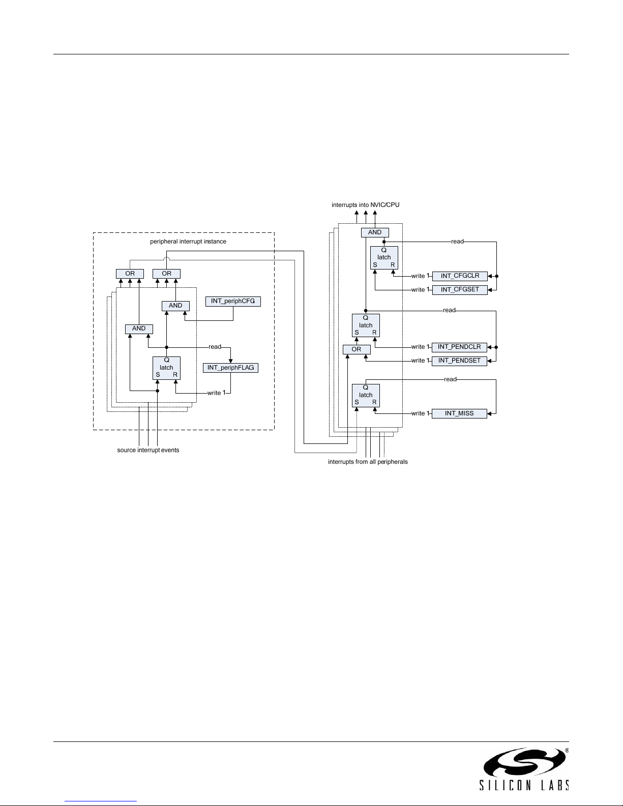
reference manual describing each peripheral. Figure 3-1 shows the Peripheral Interrupts Block Diagram.
Figure 3-1. Peripheral Interrupts Block Diagram
Given a peripheral, ‘periph’, the Event Manager registers (INT_periphCFG and INT_periphFLAG) follow the form:
INT_periphCFG enables and disables second-level interrupts. Writing 1 to a bit in the INT_periphCFG register
enables the second-level interrupt. Writing 0 to a bit in the INT_periphCFG register disables it. The
INT_periphCFG register behaves like a mask, and is responsible for allowing the INT_periphFLAG bits to
propagate into the top-level NVIC interrupts.
INT_periphFLAG indicates second-level interrupts that have occurred. Writing 1 to a bit in a INT_periphFLAG
register clears the second-level interrupt. Writing 0 to any bit in the INT_periphFLAG register is ineffective. The
INT_periphFLAG register is always active and may be set or cleared at any time, meaning if any second-level
interrupt occurs, then the corresponding bit in the INT_periphFLAG register is set regardless of the state of
INT_periphCFG.
If a bit in the INT_periphCFG register is set after the corresponding bit in the INT_periphFLAG register is set then
the second-level interrupt propagates into the top-level interrupts. The interrupt flags (signals) from the secondlevel interrupts into the top-level interrupts are level-sensitive. If a top-level NVIC interrupt is driven by a secondlevel EM interrupt, then the top-level NVIC interrupt cannot be cleared until all second-level EM interrupts are
cleared.
22 Rev. 0.4
Page 23

EM358x
The INT_periphFLAG register bits are designed to remain set if the second-level interrupt event re-occurs at the
same moment as the INT_periphFLAG register bit is being cleared. This ensures the re-occurring second-level
interrupt event is not missed.
If another enabled second-level interrupt event of the same type occurs before the first interrupt event is cleared,
the second interrupt event is lost because no counting or queuing is used. However, this condition is detected and
stored in the top-level INT_MISS register to facilitate software detection of such problems. The INT_MISS register
is “acknowledged” in the same way as the INT_periphFLAG register—by writing a 1 into the corresponding bit to
be cleared.
Table 3-2 provides a map of all peripheral interrupts. This map lists the top-level NVIC Interrupt bits and, if there is
one, the corresponding second-level EM Interrupt register bits that feed the top-level interrupts.
Table 3-2. NVIC and EM Peripheral Interrupt Map
NVIC Interrupt
(top-level)
19 INT_USB INT_USBFLAG Register 6 INT_SC2 INT_SC2FLAG register
23 INT_USBWAKEUP 12 INT_SCTXULDB
18 Reserved 4 INT_SCTXUND
17 Reserved 3 INT_SCRXOVF
16 INT_DEBUG 2 INT_SCTXIDLE
15 INT_IRQD 1 INT_SCTXFREE
EM Interrupt
(second-level)
22 INT_USBRESUME 11 INT_SCTXULDA
21 INT_USBSUSPEND 10 INT_SCRXULDB
20 INT_USBRESET 9 INT_SCRXULDA
19 INT_USBSOF 8 INT_SCNAK
18 INT_USBNAK 7 INT_SCCDMFIN
17 INT_USBPIPERXOVF 6 INT_SCTXFIN
16 INT_USBPIPETXUND 5 INT_SCRXFIN
15 INT_USBBUFRXOVF 4 INT_SCTXUND
14 INT_USBBUFTXUND 3 INT_SCRXOVF
13 INT_USBRXVALIDEP6 2 INT_SCTXIDLE
12 INT_USBRXVALIDEP5 1 INT_SCTXFREE
11 INT_USBRXVALIDEP4 0 INT_SCRXVAL
10 INT_USBRXVALIDEP3 5 INT_SC1 INT_SC1FLAG register
9 INT_USBRXVALIDEP2 14 INT_SC1PARERR
8 INT_USBRXVALIDEP1 13 INT_SC1FRMERR
7 INT_USBRXVALIDEP0 12 INT_SCTXULDB
6 INT_USBTXACTIVEEP6 11 INT_SCTXULDA
5 INT_USBTXACTIVEEP5 10 INT_SCRXULDB
4 INT_USBTXACTIVEEP4 9 INT_SCRXULDA
3 INT_USBTXACTIVEEP3 8 INT_SCNAK
2 INT_USBTXACTIVEEP2 7 INT_SCCDMFIN
1 INT_USBTXACTIVEEP1 6 INT_SCTXFIN
0 INT_USBTXACTIVEEP0 5 INT_SCRXFIN
NVIC Interrupt
(top-level)
EM Interrupt
(second-level)
Rev. 0.4 23
Page 24

EM358x
NVIC Interrupt
(top-level)
14 INT_IRQC 0 INT_SCRXVAL
13 INT_IRQB 4 INT_SLEEPTMR
12 INT_IRQA 3 INT_BB
11 INT_ADC INT_ADCFLAG register 2 INT_MGMT
4 INT_ADCOVF 1 INT_TMR2 INT_TMR2FLAG register
10 INT_MACRX 1 INT_TMRCC1IF
9 INT_MACTX 0 INT_TMRUIF
8 INT_MACTMR 0 INT_TMR1 INT_TMR1FLAG register
7 INT_SEC 6 INT_TMRTIF
4 INT_TMRCC4IF
EM Interrupt
(second-level)
3 INT_ADCSAT 6 INT_TMRTIF
2 INT_ADCULDFULL 4 INT_TMRCC4IF
1 INT_ADCULDHALF 3 INT_TMRCC3IF
0 INT_ADCDATA 2 INT_TMRCC2IF
NVIC Interrupt
(top-level)
EM Interrupt
(second-level)
3 INT_TMRCC3IF
2 INT_TMRCC2IF
1 INT_TMRCC1IF
0 INT_TMRUIF
3.3 Non-maskable Interrupt (NMI)
The non-maskable interrupt (NMI) is a special case. Despite being one of the 10 standard ARM® CortexTM-M3
NVIC interrupts, it is sourced from the Event Manager like a peripheral interrupt. The NMI has two second-level
sources; failure of the 24 MHz crystal and watchdog low water mark.
1. Failure of the 24MHz crystal: If the EM358x’s main clock, SYSCLK, is operating from the 24 MHz crystal and
the crystal fails, the EM358x detects the failure and automatically switches to the internal 12 MHz RC clock.
When this failure detection and switch has occurred, the EM358x triggers the CLK24M_FAIL second-level
interrupt, which then triggers the NMI.
2. Watchdog low water mark: If the EM358x’s watchdog is active and the watchdog counter has not been reset
for nominally 1.792 seconds, the watchdog triggers the WATCHDOG_INT second-level interrupt, which then
triggers the NMI.
24 Rev. 0.4
Page 25

EM358x
3.4 Faults
Four of the exceptions in the NVIC are faults: Hard Fault, Memory Fault, Bus Fault, and Usage Fault. Of these,
three (Hard Fault, Memory Fault, and Usage Fault) are standard ARM
The Bus Fault, though, is derived from EM358x-specific sources. The Bus Fault sources are recorded in the
SCS_AFSR register. Note that it is possible for one access to set multiple SCS_AFSR bits. Also note that MPU
configurations could prevent most of these bus fault accesses from occurring, with the advantage that illegal
writes are made precise faults. The four bus faults are:
WRONGSIZE – Generated by an 8-bit or 16-bit read or write of an APB peripheral register. This fault can also
result from an unaligned 32-bit access.
PROTECTED – Generated by a user mode (unprivileged) write to a system APB or AHB peripheral or
protected RAM (see Chapter 2, Section 2.2.2.3).
RESERVED – Generated by a read or write to an address within an APB peripheral’s 4 kB block range, but
the address is above the last physical register in that block range. Also generated by a read or write to an
address above the top of RAM or flash.
MISSED – Generated by a second SCS_AFSR fault. In practice, this bit is not seen since a second fault also
generates a hard fault, and the hard fault preempts the bus fault.
®
CortexTM-M3 exceptions.
Rev. 0.4 25
Page 26

EM358x
3.5 Registers
INT_CFGSET
Top-Level Set Interrupts Configuration Register Address: 0xE000E100 Reset: 0x0
31 30 29 28 27 26 25 24
0 0 0 0 0 0 0 0
23 22 21 20 19 18 17 16
0 0 0 0 INT_USB INT_RSVD18 INT_RSVD17 INT_DEBUG
15 14 13 12 11 10 9 8
INT_IRQD INT_IRQC INT_IRQB INT_IRQA INT_ADC INT_MACRX INT_MACTX INT_MACTMR
7 6 5 4 3 2 1 0
INT_SEC INT_SC2 INT_SC1 INT_SLEEPTMR INT_BB INT_MGMT INT_TIM2 INT_TIM1
Bitname Bitfield Access Description
INT_USB [19] RW Write 1 to enable USB interrupt. (Writing 0 has no effect.) (where
applicable)
INT_RSVD18 [18] RW Reserved: this bit should be ignored.
INT_RSVD17 [17] RW Reserved: this bit should be ignored.
INT_DEBUG [16] RW Write 1 to enable debug interrupt. (Writing 0 has no effect.)
INT_IRQD [15] RW Write 1 to enable IRQD interrupt. (Writing 0 has no effect.)
INT_IRQC [14] RW Write 1 to enable IRQC interrupt. (Writing 0 has no effect.)
INT_IRQB [13] RW Write 1 to enable IRQB interrupt. (Writing 0 has no effect.)
INT_IRQA [12] RW Write 1 to enable IRQA interrupt. (Writing 0 has no effect.)
INT_ADC [11] RW Write 1 to enable ADC interrupt. (Writing 0 has no effect.)
INT_MACRX [10] RW Write 1 to enable MAC receive interrupt. (Writing 0 has no effect.)
INT_MACTX [9] RW Write 1 to enable MAC transmit interrupt. (Writing 0 has no effect.)
INT_MACTMR [8] RW Write 1 to enable MAC timer interrupt. (Writing 0 has no effect.)
INT_SEC [7] RW Write 1 to enable security interrupt. (Writing 0 has no effect.)
INT_SC2 [6] RW Write 1 to enable serial controller 2 interrupt. (Writing 0 has no effect.)
INT_SC1 [5] RW Write 1 to enable serial controller 1 interrupt. (Writing 0 has no effect.)
INT_SLEEPTMR [4] RW Write 1 to enable sleep timer interrupt. (Writing 0 has no effect.)
INT_BB [3] RW Write 1 to enable baseband interrupt. (Writing 0 has no effect.)
INT_MGMT [2] RW Write 1 to enable management interrupt. (Writing 0 has no effect.)
INT_TIM2 [1] RW Write 1 to enable timer 2 interrupt. (Writing 0 has no effect.)
INT_TIM1 [0] RW Write 1 to enable timer 1 interrupt. (Writing 0 has no effect.)
26 Rev. 0.4
Page 27

EM358x
INT_CFGCLR
Top-Level Clear Interrupts Configuration Register Address: 0xE000E180 Reset: 0x0
31 30 29 28 27 26 25 24
0 0 0 0 0 0 0 0
23 22 21 20 19 18 17 16
0 0 0 0 INT_USB INT_RSVD18 INT_RSVD17 INT_DEBUG
15 14 13 12 11 10 9 8
INT_IRQD INT_IRQC INT_IRQB INT_IRQA INT_ADC INT_MACRX INT_MACTX INT_MACTMR
7 6 5 4 3 2 1 0
INT_SEC INT_SC2 INT_SC1 INT_SLEEPTMR INT_BB INT_MGMT INT_TIM2 INT_TIM1
Bitname Bitfield Access Description
INT_USB [19] RW Write 1 to disable USB interrupt. (Writing 0 has no effect.) (where
applicable)
INT_RSVD18 [18] RW Reserved: this bit should be ignored.
INT_RSVD17 [17] RW Reserved: this bit should be ignored.
INT_DEBUG [16] RW Write 1 to disable debug interrupt. (Writing 0 has no effect.)
INT_IRQD [15] RW Write 1 to disable IRQD interrupt. (Writing 0 has no effect.)
INT_IRQC [14] RW Write 1 to disable IRQC interrupt. (Writing 0 has no effect.)
INT_IRQB [13] RW Write 1 to disable IRQB interrupt. (Writing 0 has no effect.)
INT_IRQA [12] RW Write 1 to disable IRQA interrupt. (Writing 0 has no effect.)
INT_ADC [11] RW Write 1 to disable ADC interrupt. (Writing 0 has no effect.)
INT_MACRX [10] RW Write 1 to disable MAC receive interrupt. (Writing 0 has no effect.)
INT_MACTX [9] RW Write 1 to disable MAC transmit interrupt. (Writing 0 has no effect.)
INT_MACTMR [8] RW Write 1 to disable MAC timer interrupt. (Writing 0 has no effect.)
INT_SEC [7] RW Write 1 to disable security interrupt. (Writing 0 has no effect.)
INT_SC2 [6] RW Write 1 to disable serial controller 2 interrupt. (Writing 0 has no effect.)
INT_SC1 [5] RW Write 1 to disable serial controller 1 interrupt. (Writing 0 has no effect.)
INT_SLEEPTMR [4] RW Write 1 to disable sleep timer interrupt. (Writing 0 has no effect.)
INT_BB [3] RW Write 1 to disable baseband interrupt. (Writing 0 has no effect.)
INT_MGMT [2] RW Write 1 to disable management interrupt. (Writing 0 has no effect.)
INT_TIM2 [1] RW Write 1 to disable timer 2 interrupt. (Writing 0 has no effect.)
INT_TIM1 [0] RW Write 1 to disable timer 1 interrupt. (Writing 0 has no effect.)
Rev. 0.4 27
Page 28

EM358x
INT_PENDSET
Top-Level Set Interrupts Pending Register Address: 0xE000E200 Reset: 0x0
31 30 29 28 27 26 25 24
0 0 0 0 0 0 0 0
23 22 21 20 19 18 17 16
0 0 0 0 INT_USB INT_RSVD18 INT_RSVD17 INT_DEBUG
15 14 13 12 11 10 9 8
INT_IRQD INT_IRQC INT_IRQB INT_IRQA INT_ADC INT_MACRX INT_MACTX INT_MACTMR
7 6 5 4 3 2 1 0
INT_SEC INT_SC2 INT_SC1 INT_SLEEPTMR INT_BB INT_MGMT INT_TIM2 INT_TIM1
Bitname Bitfield Access Description
INT_USB [19] RW Write 1 to pend USB interrupt. (Writing 0 has no effect.) (where applicable)
INT_RSVD18 [18] RW Reserved: this bit should be ignored.
INT_RSVD17 [17] RW Reserved: this bit should be ignored.
INT_DEBUG [16] RW Write 1 to pend debug interrupt. (Writing 0 has no effect.)
INT_IRQD [15] RW Write 1 to pend IRQD interrupt. (Writing 0 has no effect.)
INT_IRQC [14] RW Write 1 to pend IRQC interrupt. (Writing 0 has no effect.).
INT_IRQB [13] RW Write 1 to pend IRQB interrupt. (Writing 0 has no effect.)
INT_IRQA [12] RW Write 1 to pend IRQA interrupt. (Writing 0 has no effect.)
INT_ADC [11] RW Write 1 to pend ADC interrupt. (Writing 0 has no effect.)
INT_MACRX [10] RW Write 1 to pend MAC receive interrupt. (Writing 0 has no effect.)
INT_MACTX [9] RW Write 1 to pend MAC transmit interrupt. (Writing 0 has no effect.)
INT_MACTMR [8] RW Write 1 to pend MAC timer interrupt. (Writing 0 has no effect.)
INT_SEC [7] RW Write 1 to pend security interrupt. (Writing 0 has no effect.)
INT_SC2 [6] RW Write 1 to pend serial controller 2 interrupt. (Writing 0 has no effect.)
INT_SC1 [5] RW Write 1 to pend serial controller 1 interrupt. (Writing 0 has no effect.)
INT_SLEEPTMR [4] RW Write 1 to pend sleep timer interrupt. (Writing 0 has no effect.)
INT_BB [3] RW Write 1 to pend baseband interrupt. (Writing 0 has no effect.)
INT_MGMT [2] RW Write 1 to pend management interrupt. (Writing 0 has no effect.)
INT_TIM2 [1] RW Write 1 to pend timer 2 interrupt. (Writing 0 has no effect.)
INT_TIM1 [0] RW Write 1 to pend timer 1 interrupt. (Writing 0 has no effect.)
28 Rev. 0.4
Page 29

EM358x
INT_PENDCLR
Top-Level Clear Interrupts Pending Register Address: 0xE000E280 Reset: 0x0
31 30 29 28 27 26 25 24
0 0 0 0 0 0 0 0
23 22 21 20 19 18 17 16
0 0 0 0 INT_USB INT_RSVD18 INT_RSVD17 INT_DEBUG
15 14 13 12 11 10 9 8
INT_IRQD INT_IRQC INT_IRQB INT_IRQA INT_ADC INT_MACRX INT_MACTX INT_MACTMR
7 6 5 4 3 2 1 0
INT_SEC INT_SC2 INT_SC1 INT_SLEEPTMR INT_BB INT_MGMT INT_TIM2 INT_TIM1
Bitname Bitfield Access Description
INT_USB [19] RW Write 1 to unpend USB interrupt. (Writing 0 has no effect.) (where
applicable)
INT_RSVD18 [18] RW Reserved: this bit should be ignored.
INT_RSVD17 [17] RW Reserved: this bit should be ignored.
INT_DEBUG [16] RW Write 1 to unpend debug interrupt. (Writing 0 has no effect.)
INT_IRQD [15] RW Write 1 to unpend IRQD interrupt. (Writing 0 has no effect.)
INT_IRQC [14] RW Write 1 to unpend IRQC interrupt. (Writing 0 has no effect.)
INT_IRQB [13] RW Write 1 to unpend IRQB interrupt. (Writing 0 has no effect.)
INT_IRQA [12] RW Write 1 to unpend IRQA interrupt. (Writing 0 has no effect.)
INT_ADC [11] RW Write 1 to unpend ADC interrupt. (Writing 0 has no effect.)
INT_MACRX [10] RW Write 1 to unpend MAC receive interrupt. (Writing 0 has no effect.)
INT_MACTX [9] RW Write 1 to unpend MAC transmit interrupt. (Writing 0 has no effect.)
INT_MACTMR [8] RW Write 1 to unpend MAC timer interrupt. (Writing 0 has no effect.)
INT_SEC [7] RW Write 1 to unpend security interrupt. (Writing 0 has no effect.)
INT_SC2 [6] RW Write 1 to unpend serial controller 2 interrupt. (Writing 0 has no effect.)
INT_SC1 [5] RW Write 1 to unpend serial controller 1 interrupt. (Writing 0 has no effect.)
INT_SLEEPTMR [4] RW Write 1 to unpend sleep timer interrupt. (Writing 0 has no effect.)
INT_BB [3] RW Write 1 to unpend baseband interrupt. (Writing 0 has no effect.)
INT_MGMT [2] RW Write 1 to unpend management interrupt. (Writing 0 has no effect.)
INT_TIM2 [1] RW Write 1 to unpend timer 2 interrupt. (Writing 0 has no effect.)
INT_TIM1 [0] RW Write 1 to unpend timer 1 interrupt. (Writing 0 has no effect.)
Rev. 0.4 29
Page 30

EM358x
INT_ACTIVE
Top-Level Active Interrupts Register Address: 0xE000E300 Reset: 0x0
31 30 29 28 27 26 25 24
0 0 0 0 0 0 0 0
23 22 21 20 19 18 17 16
0 0 0 0 INT_USB INT_RSVD18 INT_RSVD17 INT_DEBUG
15 14 13 12 11 10 9 8
INT_IRQD INT_IRQC INT_IRQB INT_IRQA INT_ADC INT_MACRX INT_MACTX INT_MACTMR
7 6 5 4 3 2 1 0
INT_SEC INT_SC2 INT_SC1 INT_SLEEPTMR INT_BB INT_MGMT INT_TIM2 INT_TIM1
Bitname Bitfield Access Description
INT_USB [19] RW USB interrupt active (where applicable)
INT_RSVD18 [18] RW Reserved: this bit should be ignored.
INT_RSVD17 [17] RW Reserved: this bit should be ignored.
INT_DEBUG [16] R Debug interrupt active.
INT_IRQD [15] R IRQD interrupt active.
INT_IRQC [14] R IRQC interrupt active.
INT_IRQB [13] R IRQB interrupt active.
INT_IRQA [12] R IRQA interrupt active.
INT_ADC [11] R ADC interrupt active.
INT_MACRX [10] R MAC receive interrupt active.
INT_MACTX [9] R MAC transmit interrupt active.
INT_MACTMR [8] R MAC timer interrupt active.
INT_SEC [7] R Security interrupt active.
INT_SC2 [6] R Serial controller 2 interrupt active.
INT_SC1 [5] R Serial controller 1 interrupt active.
INT_SLEEPTMR [4] R Sleep timer interrupt active.
INT_BB [3] R Baseband interrupt active.
INT_MGMT [2] R Management interrupt active.
INT_TIM2 [1] R Timer 2 interrupt active.
INT_TIM1 [0] R Timer 1 interrupt active.
30 Rev. 0.4
Page 31

EM358x
INT_MISS
Top-Level Missed Interrupts Register Address: 0x4000A820 Reset: 0x0
31 30 29 28 27 26 25 24
0 0 0 0 0 0 0 0
23 22 21 20 19 18 17 16
0 0 0 0 INT_MISSUSB INT_RSVD18 INT_RSVD17 0
15 14 13 12 11 10 9 8
INT_MISSIRQD INT_MISSIRQC INT_MISSIRQB INT_MISSIRQA INT_MISSADC INT_MISSMACRX INT_MISSMACTX INT_MISSMACTMR
7 6 5 4 3 2 1 0
INT_MISSSEC INT_MISSSC2 INT_MISSSC1 INT_MISSSLEEP INT_MISSBB INT_MISSMGMT 0 0
Bitname Bitfield Access Description
INT_MISSUSB [19] RW USB interrupt missed (where applicable)
INT_RSVD18 [18] RW Reserved: this bit should be ignored.
INT_RSVD17 [17] RW Reserved: this bit should be ignored.
INT_MISSIRQD [15] RW IRQD interrupt missed.
INT_MISSIRQC [14] RW IRQC interrupt missed.
INT_MISSIRQB [13] RW IRQB interrupt missed.
INT_MISSIRQA [12] RW IRQA interrupt missed.
INT_MISSADC [11] RW ADC interrupt missed.
INT_MISSMACRX [10] RW MAC receive interrupt missed.
INT_MISSMACTX [9] RW MAC transmit interrupt missed.
INT_MISSMACTMR [8] RW MAC Timer interrupt missed.
INT_MISSSEC [7] RW Security interrupt missed.
INT_MISSSC2 [6] RW Serial controller 2 interrupt missed.
INT_MISSSC1 [5] RW Serial controller 1 interrupt missed.
INT_MISSSLEEP [4] RW Sleep timer interrupt missed.
INT_MISSBB [3] RW Baseband interrupt missed.
INT_MISSMGMT [2] RW Management interrupt missed.
Rev. 0.4 31
Page 32

EM358x
SCS_AFSR
Auxiliary Fault Status Register Address: 0xE000ED3C Reset: 0x0
31 30 29 28 27 26 25 24
0 0 0 0 0 0 0 0
23 22 21 20 19 18 17 16
0 0 0 0 0 0 0 0
15 14 13 12 11 10 9 8
0 0 0 0 0 0 0 0
7 6 5 4 3 2 1 0
0 0 0 0 WRONGSIZE PROTECTED RESERVED MISSED
Bitname Bitfield Access Description
WRONGSIZE [3] RW A bus fault resulted from an 8-bit or 16-bit read or write of an APB
peripheral register. This fault can also result from an unaligned 32-bit
access.
PROTECTED [2] RW A bus fault resulted from a user mode (unprivileged) write to a system APB
or AHB peripheral or protected RAM.
RESERVED [1] RW A bus fault resulted from a read or write to an address within an APB
peripheral's 4 kB block range, but above the last physical register in that
block. Can also result from a read or write to an address above the top of
RAM or flash.
MISSED [0] RW A bus fault occurred when a bit was already set in this register.
32 Rev. 0.4
Page 33

4 Radio Module
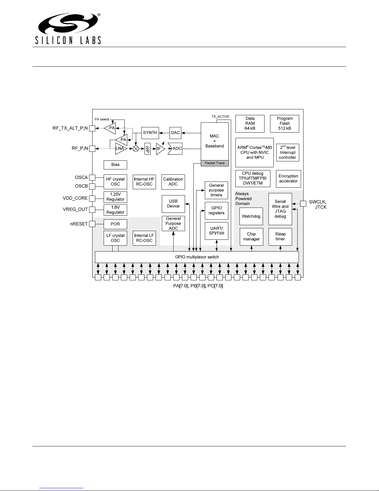
The radio module consists of an analog front end and digital baseband as shown in Figure 4-1.
EM358x
Figure 4-1. EM358 Block Diagram
4.1 Receive (Rx) Path
The Rx path uses a low-IF, super-heterodyne receiver that rejects the image frequency using complex mixing and
polyphase filtering. In the analog domain, the input RF signal from the antenna is first amplified and mixed down
to a 4 MHz IF frequency. The mixers’ output is filtered, combined, and amplified before being sampled by a 12
MSPS ADC. The digitized signal is then demodulated in the digital baseband. The filtering within the Rx path
improves the EM358x’s co-existence with other 2.4 GHz transceivers such as Zigbee/ 802.15.4-2003, IEEE
802.11-2007, and Bluetooth radios. The digital baseband also provides gain control of the Rx path, both to enable
the reception of small and large wanted signals and to tolerate large interferers.
4.1.1 Rx Baseband
The EM358x Rx digital baseband implements a coherent demodulator for optimal performance. The baseband
demodulates the O-QPSK signal at the chip level and synchronizes with the IEEE 802.15.4-2003-defined
preamble. An automatic gain control (AGC) module adjusts the analog gain continuously every ¼ symbol until the
preamble is detected. Once detected, the gain is fixed for the remainder of the packet. The baseband despreads
the demodulated data into 4-bit symbols. These symbols are buffered and passed to the hardware-based MAC
module for packet assembly and filtering.
In addition, the Rx baseband provides the calibration and control interface to the analog Rx modules, including
the LNA, Rx baseband filter, and modulation modules. The Ember software includes calibration algorithms that
use this interface to reduce the effects of silicon process and temperature variation.
Rev. 0.4 33
Page 34

EM358x
4.1.2 RSSI and CCA
The EM358x calculates the RSSI over every 8-symbol period as well as at the end of a received packet. The
linear range of RSSI is specified to be at least 40 dB over temperature. At room temperature, the linear range is
approximately 60 dB (-90 dBm to -30 dBm input signal).
The EM358x Rx baseband provides support for the IEEE 802.15.4-2003 RSSI CCA method. Clear channel
reports busy medium if RSSI exceeds its threshold.
4.2 Transmit (Tx) Path
The EM358x Tx path produces an O-QPSK-modulated signal using the analog front end and digital baseband.
The area- and power-efficient Tx architecture uses a two-point modulation scheme to modulate the RF signal
generated by the synthesizer. The modulated RF signal is fed to the integrated PA and then out of the EM358x.
4.2.1 Tx Baseband
The EM358x Tx baseband in the digital domain spreads the 4-bit symbol into its IEEE 802.15.4-2003-defined 32chip sequence. It also provides the interface for the Ember software to calibrate the Tx module to reduce silicon
process, temperature, and voltage variations.
4.2.2 TX_ACTIVE and nTX_ACTIVE Signals
For applications requiring an external PA, two signals are provided called TX_ACTIVE and nTX_ACTIVE. These
signals are the inverse of each other. They can be used for external PA power management and RF switching
logic. In transmit mode the Tx baseband drives TX_ACTIVE high, as described in Table 7-5, GPIO Signal
Assignments. In receive mode the TX_ACTIVE signal is low. TX_ACTIVE is the alternate function of PC5, and
nTX_ACTIVE is the alternate function of PC6. See Chapter 7 GPIO for details of the alternate GPIO functions.
The digital I/O that provide these signals have a 4 mA output sink and source capability.
4.3 Calibration
The Ember software calibrates the radio using dedicated hardware resources.
4.4 Integrated MAC Module
The EM358x integrates most of the IEEE 802.15.4-2003 MAC requirements in hardware. This allows the ARM®
TM
Cortex
acts as a first-line filter for unwanted packets. The EM358x MAC uses a DMA interface to RAM to further reduce
the overall ARM
When a packet is ready for transmission, the Ember software configures the Tx MAC DMA by indicating the
packet buffer RAM location. The MAC waits for the backoff period, then switches the baseband to Tx mode and
performs channel assessment. When the channel is clear the MAC reads data from the RAM buffer, calculates
the CRC, and provides 4-bit symbols to the baseband. When the final byte has been read and sent to the
baseband, the CRC remainder is read and transmitted.
The MAC is in Rx mode most of the time. In Rx mode various format and address filters keep unwanted packets
from using excessive RAM buffers, and prevent the CPU from being unnecessarily interrupted. When the
reception of a packet begins, the MAC reads 4-bit symbols from the baseband and calculates the CRC. It then
assembles the received data for storage in a RAM buffer. Rx MAC DMA provides direct access to RAM. Once the
packet has been received additional data, which provides statistical information on the packet to the Ember
software, is appended to the end of the packet in the RAM buffer space.
The primary features of the MAC are:
-M3 CPU to provide greater bandwidth to application and network operations. In addition, the hardware
®
CortexTM-M3 CPU interaction when transmitting or receiving packets.
CRC generation, appending, and checking
Hardware timers and interrupts to achieve the MAC symbol timing
Automatic preamble and SFD pre-pending on Tx packets
Address recognition and packet filtering on Rx packets
Automatic acknowledgement transmission
Automatic transmission of packets from memory
Automatic transmission after backoff time if channel is clear (CCA)
Automatic acknowledgement checking
34 Rev. 0.4
Page 35

EM358x
Time stamping received and transmitted messages
Attaching packet information to received packets (LQI, RSSI, gain, time stamp, and packet status)
IEEE 802.15.4-2003 timing and slotted/unslotted timing
4.5 Packet Trace Interface (PTI)
The EM358x integrates a true PHY-level PTI for effective network-level debugging. It monitors all the PHY Tx and
Rx packets between the MAC and baseband modules without affecting their normal operation. It cannot be used
to inject packets into the PHY/MAC interface. This 500 kbps asynchronous interface comprises the frame signal
(PTI_EN, PA4) and the data signal (PTI_DATA, PA5). PTI is supported by the Ember development tools.
4.6 Random Number Generator
Thermal noise in the analog circuitry is digitized to provide entropy for a true random number generator (TRNG).
The TRNG produces 16-bit uniformly distributed numbers. The Ember software uses the TRNG to seed a pseudo
random number generator (PRNG). The TRNG is also used directly for cryptographic key generation.
Rev. 0.4 35
Page 36

EM358x
5 System Modules
System modules encompass power domains, resets, clocks, system timers, power management, and encryption.
Figure 5-1 shows these modules and how they interact.
OSCRC
External
Regulator
recomended
connections for
internal regulator
optional
connections for
external regulator
REG_EN
VDD_PADS
VREG_OUT
VDD_MEM
VDD_CORE
nRESET
JRST
VREG_1V25
VREG_1V8
Reset Filter
SWJ
JTAG-TAP
sleep timer compare b
WAKE_CORE
CDBGPWRUPREQ
CSYSPWRUPREQ
sleep timer compare a
sleep timer wrap
Wakeup Recording
Power Management
always-on supply
mem supply
core supply
CDBGRSTREQ
PB2
IRQD
WatchdogSleep Timer
POR HV
POR LVmem
POR LVcore
DIV10CLK1K
CLK32K
GPIO wake monitoring
PA2
deep sleep
wakeup
watchdog
POR HV
Reset Recording
POR LV
Reset Generation
OSC32K
OSC32A
OSC32B
always-on domain
mem supply
Flash
mem domain
always-on supply
core domain
option byte error
FLITF
RAM
Figure 5-1. System Module Block Diagram
36 Rev. 0.4
SYSRESETREQ
ARM®
Cortex
-M3
CPU
ARM®
Cortex
-M3
Debug
Security Accelerator
PORESET
SYSRESET
SYSCLK
DAPRESET
PRESET
PRESET
AHB-AP
registers
HV
registers
LV
OSCHF
OSC24M
clock switch
OSCA
OSCB
Page 37

EM358x
5.1 Power domains
The EM358x contains three power domains:
An “always-on domain” containing all logic and analog cells required to manage the EM358x’s power modes,
including the GPIO controller and sleep timer. This domain must remain powered.
A “core domain” containing the CPU, Nested Vectored Interrupt Controller (NVIC), and peripherals. To save
power, this domain can be powered down using a mode called deep sleep. In the EM358 the core domain also
includes the RAM, which by default is powered down in deep sleep. An additional feature of the RAM is that
blocks of RAM cells can optionally be retained in deep sleep. This is configured using a register, which must
be written before entering deep sleep.
A “flash domain” containing the flash memory. This domain is managed by the power management controller.
During deep sleep the flash portion is completely powered down.
5.1.1 Internally regulated power
The preferred and recommended power configuration is to use the internal regulated power supplies to provide
power to the core and memory domains. The internal regulators (VREG_1V25 and VREG_1V8) generate nominal
1.25 V and 1.8 V supplies. The 1.25 V supply is internally routed to the core domain, RAM, and to an external pin.
The 1.8 V supply is routed to an external pin where it can be externally routed back into the chip to supply the
memory domain. The internal regulators are described in Chapter 6, Integrated Voltage Regulator.
When using the internal regulators, the always-on domain must be powered between 2.1 V and 3.6 V at all four
VDD_PADS pins.
When using the internal regulators, the VREG_1V8 regulator output pin (VREG_OUT) must be connected to the
VDD_MEM, VDD_PADSA, VDD_VCO, VDD_RF, VDD_IF, VDD_PRE, and VDD_SYNTH pins.
When using the internal regulators, the VREG_1V25 regulator output and supply requires a connection between
both VDD_CORE pins.
5.1.2 Externally regulated power
Optionally, the on-chip regulators may be left unused, and the core and memory domains may instead be
powered from external supplies. The nominal supply voltages of the internal power domains must be respected,
that is core and RAM at nominally 1.25 V and flash at nominally 1.8 V. A regulator enable signal, REG_EN, is
provided for control of external regulators. This is an open-drain signal that requires an external pull-up resistor. If
REG_EN is not required to control external regulators it can be disabled (see section 7.3, Forced Functions in
Chapter 7, GPIO).
Using an external regulator requires the always-on domain to be powered between 1.8 V and 3.6 V at all four
VDD_PADS pins.
When using an external regulator, the VREG_1V8 regulator output pin (VREG_OUT) must be left unconnected.
When using an external regulator, the external nominal 1.25 V supply has to be connected to VDD_CORE pins.
The external nominal 1.8 V supply must be connected to the VDD_MEM, VDD_PADSA, VDD_VCO, VDD_RF,
VDD_IF, VDD_PRE and VDD_SYNTH pins.
5.2 Resets
The EM358x resets are generated from a number of sources. Each of these reset sources feeds into central reset
detection logic that causes various parts of the system to be reset depending on the state of the system and the
nature of the reset event.
5.2.1 Reset Sources
5.2.1.1 Power-On-Resets (POR HV and POR LV)
The EM358x measures the voltage levels supplied to the three power domains. If a supply voltage drops below a
low threshold, then a reset is applied. The reset is released if the supply voltage rises above a high threshold.
There are three detection circuits for power-on-reset as follows:
POR HV monitors the always-on domain supply voltage. Thresholds are given in Table 5-1.
POR LVcore monitors the core domain supply voltage. Thresholds are given in Table 5-2.
POR LVmem monitors the memory supply voltage. Thresholds are given in Table 5-3.
Rev. 0.4 37
Page 38

EM358x
Table 5-1. POR HV Thresholds
Parameter Test conditions Min Typ Max Unit
Always-on domain release 0.62 0.95 1.20 V
Always-on domain assert 0.45 0.65 0.85 V
Supply rise time From 0.5 V to 1.7 V 250 µs
Table 5-2. POR LVcore Thresholds
Parameter Test conditions Min Typ Max Unit
1.25 V domain release 0.9 1.0 1.1 V
1.25 V domain assert 0.8 0.9 1.0 V
Table 5-3 POR LVmem Thresholds
Parameter Test conditions Min Typ Max Unit
1.8 V domain release 1.35 1.5 1.65 V
1.8 V domain assert 1.26 1.4 1.54 V
The POR LVcore and POR LVmem reset sources are merged to provide a single reset source, POR LV, to the
Reset Generation module, since the detection of either event needs to reset the same system modules.
5.2.1.2 nRESET Pin
A single active low pin, nRESET, is provided to reset the system. This pin has a Schmitt triggered input.
To afford good noise immunity and resistance to switch bounce, the pin is filtered with the Reset Filter module
and generates the pin reset source, nRESET, to the Reset Generation module. Table 5-4 contains the
specification for the filter.
Table 5-4. Reset Filter Specification for nRESET
Parameter Min Typ Max Unit
Reset filter time constant 2.1 12.0 16.0 µs
Reset pulse width to guarantee a reset 26.0 µs
Reset pulse width guaranteed not to cause a reset 0 1.0 µs
5.2.1.3 Watchdog Reset
The EM358x contains a watchdog timer (see also the Watchdog Timer section) that is clocked by the internal
1 kHz timing reference. When the timer expires it generates the reset source WATCHDOG_RESET to the Reset
Generation module.
5.2.1.4 Software Reset
The ARM® CortexTM-M3 CPU can initiate a reset under software control. This is indicated with the reset source
SYSRESETREQ to the Reset Generation module.
5.2.1.5 Option Byte Error
The flash memory controller contains a state machine that reads configuration information from the information
blocks in the flash at system start time. An error check is performed on the option bytes that are read from flash
and, if the check fails, an error is signaled that provides the reset source OPT_BYTE_ERROR to the Reset
Generation module.
38 Rev. 0.4
Page 39

EM358x
If an option byte error is detected, the system restarts and the read and check process is repeated. If the error is
detected again the process is repeated but stops on the 3
deep sleep where recovery is possible. In this state, flash memory readout protection is forced active to prevent
secure applications from being compromised.
5.2.1.6 Debug Reset
The Serial Wire/JTAG Interface (SWJ) provides access to the SWJ Debug Port (SWJ-DP) registers. By setting
the register bit CDBGRSTREQ in the SWJ-DP, the reset source CDBGRSTREQ is provided to the Reset
Generation module.
5.2.1.7 JRST
One of the EM358x’s pins can function as the JTAG reset, conforming to the requirements of the JTAG standard.
This input acts independently of all other reset sources and, when asserted, does not reset any on-chip hardware
except for the JTAG TAP. If the EM358x is in the Serial Wire mode or if the SWJ is disabled, this input has no
effect.
5.2.1.8 Deep Sleep Reset
The Power Management module informs the Reset Generation module of entry into and exit from the deep sleep
states. The deep sleep reset is applied in the following states: before entry into deep sleep, while removing power
from the memory and core domain, while in deep sleep, while waking from deep sleep, and while reapplying
power until reliable power levels have been detect by POR LV.
The Power Management module allows a special emulated deep sleep state that retains memory and core
domain power while in deep sleep.
5.2.2 Reset Recording
The EM358x records the last reset condition that generated a restart to the system. The reset conditions recorded
are:
POR HV always-on domain power supply failure
POR LV core domain (POR LVcore) or memory domain (POR LVmem) power supply failure
nRESET pin reset asserted
watchdog watchdog timer expired
SYSRESETREQ software reset by SYSERSETREQ from ARM® CortexTM-M3 CPU
deep sleep wakeup wake-up from deep sleep
option byte error error check failed when reading option bytes from flash
Note: While CPU Lockup is shown as a reset condition in software, CPU Lockup is not specifically a reset event.
CPU Lockup is set to indicate that the CPU entered an unrecoverable exception. Execution stops but a
reset is not applied. This is so that a debugger can interpret the cause of the error. Silicon Labs
recommends that in a live application (in other words, no debugger attached) the watchdog be enabled by
default so that the EM358x can be restarted.
5.2.3 Reset Generation Module
The Reset Generation module responds to reset sources and generates the following reset signals:
PORESET Reset of the ARM® CortexTM-M3 CPU and ARM® CortexTM-M3 System Debug components (Flash Patch and
SYSRESET Reset of the ARM® CortexTM-M3 CPU without resetting the Core Debug and System Debug components,
DAPRESET Reset to the SWJ’s AHB Access Port (AHB-AP)
PRESETHV Peripheral reset for always-on power domain, for peripherals that are required to retain their
PRESETLV Peripheral reset for core power domain, for peripherals that are not required to retain their
Breakpoint, Data Watchpoint and Trace, Instrumentation Trace Macrocell, Nested Vectored Interrupt
Controller). ARM defines PORESET as the region that is reset when power is applied.
so that a live system can be reset without disturbing the debug configuration.
configuration across a deep sleep cycle
configuration across a deep sleep cycle
rd
failure. The system is then placed into an emulated
Rev. 0.4 39
Page 40

EM358x
Table 5-5 shows which reset sources generate certain resets.
Table 5-5. Generated Resets
Reset Source Reset Generation Module Output
PORESET SYSRESET DAPRESET PRESETHV PRESETLV
POR HV X X X X X
POR LV (due to waking from
normal deep sleep)
POR LV (not due to waking from
normal deep sleep)
nRESET X X X X
Watchdog X X X
SYSRESETREQ X X X
Option byte error X X X
Normal deep sleep X X X X
Emulated deep sleep X X
Debug reset X
X X X X
X X X X X
5.3 Clocks
The EM358 integrates four oscillators:
12 MHz RC oscillator
24 MHz crystal oscillator
10 kHz RC oscillator
32.768 kHz crystal oscillator
40 Rev. 0.4
Page 41

EM358x
Figure 5-2 shows a block diagram of the clocks in the EM358x. This simplified view shows all the clock sources
and the general areas of the chip to which they are routed.
Rev. 0.4 41
Figure 5-2. Clocks Block Diagram
Page 42

EM358x
5.3.1 High-Frequency Internal RC Oscillator (OSCHF)
The high-frequency RC oscillator (OSCHF) is used as the default system clock source when power is applied to
the core domain. The nominal frequency coming out of reset is 12 MHz and Ember software calibrates this clock
to 12 MHz. Table 5-6 contains the specification for the high frequency RC oscillator.
Most peripherals, excluding the radio peripheral, are fully functional using the OSCHF clock source. Application
software must be aware that peripherals are clocked at different speeds depending on whether OSCHF or
OSC24M is being used. Since the frequency step of OSCHF is 0.3 MHz and the high-frequency crystal oscillator
is used for calibration, the calibrated accuracy of OSCHF is ±150 kHz ±40 ppm. The UART and ADC peripherals
may not be usable due to the lower accuracy of the OSCHF frequency.
Table 5-6. High-Frequency RC Oscillator Specification
Parameter Test conditions Min Typ Max Unit
Frequency at reset 6 12 20 MHz
Frequency Steps 0.3 MHz
Duty cycle 40 60 %
Supply dependence Change in supply = 0.1 V
Test at supply changes: 1.8 V to 1.7 V
5.3.2 High-Frequency Crystal Oscillator (OSC24M)
The high-frequency crystal oscillator (OSC24M) requires an external 24 MHz crystal with an accuracy of ±40 ppm.
Based upon the application’s bill of materials and current consumption requirements, the external crystal may
cover a range of ESR requirements. Table 5-7 contains the specification for the high frequency crystal oscillator.
The crystal oscillator has a software-programmable bias circuit to minimize current consumption. Ember software
configures the bias circuit for minimum current consumption.
All peripherals including the radio peripheral are fully functional using the OSC24M clock source. Application
software must be aware that peripherals are clocked at different speeds depending on whether OSCHF or
OSC24M is being used.
If the 24 MHz crystal fails, a hardware failover mechanism forces the system to switch back to the high-frequency
RC oscillator as the main clock source, and a non-maskable interrupt (NMI) is signaled to the ARM
NVIC.
5 %
®
CortexTM-M3
Table 5-7. High-Frequency Crystal Oscillator Specification
Parameter Test conditions Min Typ Max Unit
Frequency 24 MHz
Accuracy -40 +40 ppm
Duty cycle 40 60 %
Start-up time at max bias 1 ms
Start up time at optimal bias 2 ms
Current consumption 200 300 μA
Current consumption at max bias 1 mA
42 Rev. 0.4
Page 43

EM358x
Parameter Test conditions Min Typ Max Unit
Crystal with high ESR 100 Ω
Load capacitance 10 pF
Crystal capacitance 7 pF
Crystal power dissipation 200 µW
Crystal with low ESR 60 Ω
Load capacitance 18 pF
Crystal capacitance 7 pF
Crystal power dissipation 1 mW
5.3.3 Low-Frequency Internal RC Oscillator (OSCRC)
A low-frequency RC oscillator (OSCRC) is provided as an internal timing reference. The nominal frequency
coming out of reset is 10 kHz, and Ember software calibrates this clock to 10 kHz. From the tuned 10 kHz
oscillator (OSCRC) Ember software calibrates a fractional-N divider to produce a 1 kHz reference clock, CLK1K.
Table 5-8 contains the specification for the low frequency RC oscillator.
Table 5-8. Low-Frequency RC Oscillator Specification
Parameter Test conditions Min Typ Max Unit
Nominal Frequency After trimming 9 10 11 kHz
Analog trim step size 0.5 kHz
Supply dependence For a voltage drop from 3.6 V to 3.1 V or 2.6 V to 2.1 V
(without re-calibration)
Temperature dependence Frequency variation with temperature for a change
from -40
(without re-calibration)
5.3.4 Low-Frequency Crystal Oscillator (OSC32K)
A low-frequency 32.768 kHz crystal oscillator (OSC32K) is provided as an optional timing reference for on-chip
timers. This oscillator is designed for use with an external watch crystal. When using the 32.768 kHz crystal, you
must connect it to GPIO PC6 and PC7, and must configure these two GPIOs for analog input. Alternatively, when
PC7 is configured as a digital input, PC7 can accept an external digital clock input instead of a 32.786 kHz crystal.
The digital clock input signal must be a 1 V peak-to-peak sine wave with a DC bias of 0.5 V. Refer to Chapter 7,
GPIO, for GPIO configuration details. Using the low-frequency oscillator, crystal or digital clock, is enabled
through Ember software.
Table 5-9 contains the specification for the low frequency crystal oscillator.
o
C to +85oC
1 %
2 %
Table 5-9. Low-Frequency Crystal Oscillator Specification
Parameter Test conditions Min Typ Max Unit
Frequency 32.768 kHz
Accuracy At 25ºC -20 +20 ppm
Load capacitance OSC32A 27 pF
Load capacitance OSC32B 18 pF
Rev. 0.4 43
Page 44

EM358x
Parameter Test conditions Min Typ Max Unit
Crystal ESR 100 kΩ
Start-up time 2 s
Current consumption At 25°C, VDD_PADS=3.0 V 0.5 μA
5.3.5 Clock Switching
The EM358x has two switching mechanisms for the main system clock, providing four clock modes. Table 5-10
shows these clock modes and how they affect the internal clocks.
The register bit OSC24M_CTRL_OSC24M_SEL in the OSC24M_CTRL register switches between the highfrequency RC oscillator (OSCHF) and the high-frequency crystal oscillator (OSC24M) as the main system clock
(SYSCLK). The peripheral clock (PCLK) is always half the frequency of SYSCLK.
The register bit CPU_CLKSEL_FIELD in the CPU_CLKSEL register switches between PCLK and SYSCLK to
produce the ARM
CPU at the higher PCLK frequency, 24 MHz, to give higher processing performance for all applications and
improved duty cycling for applications using sleep modes.
The register bit USBSUSP_CLKSEL_FIELD in the CPU_CLKSEL register is used to divide the whole clock tree
by 4 when the EM358x (variants that support USB) is operating as a bus-powered USB device and USB
suspends the EM358x. Refer to Chapter 9, USB, for USB details.
In addition to these modes, further automatic control is invoked by hardware when flash programming is enabled.
To ensure accuracy of the flash controller’s timers, the FCLK frequency is forced to 12 MHz during flash
programming and erase operations.
®
CortexTM-M3 CPU clock (FCLK). The default and preferred mode of operation is to run the
Table 5-10. System Clock Modes
FCLK
OSC24M_CTRL_OSC24M_SEL CPU_CLKSEL_FIELD SYSCLK PCLK
Flash
Program/Erase
Inactive
Flash
Program/Erase
Active
0 (OSCHF) 0 (Normal CPU) 12 MHz 6 MHz 6 MHz 12 MHz
0 (OSCHF) 1 (Fast CPU) 12 MHz 6 MHz 12 MHz 12 MHz
1 (OSC24M) 0 (Normal CPU) 24 MHz 12 MHz 12 MHz 12 MHz
1 (OSC24M) 1 (Fast CPU) 24 MHz 12 MHz 24 MHz 12 MHz
5.4 System Timers
5.4.1 Watchdog Timer
The EM358x integrates a watchdog timer which can be enabled to provide protection against software crashes
and ARM
watchdog timer uses the calibrated 1 kHz clock (CLK1K) as its reference and provides a nominal 2.048 s timeout.
A low water mark interrupt occurs at 1.792 s and triggers an NMI to the ARM
warning. When the watchdog is enabled, the timer must be periodically reset before it expires. The watchdog
timer is paused when the debugger halts the ARM
implements deep sleep functionality disables the watchdog when entering deep sleep and restores the watchdog,
if it was enabled, when exiting deep sleep.
Ember software provides an API for enabling, resetting, and disabling the watchdog timer.
®
CortexTM-M3 CPU lockup. By default, it is disabled at power up of the always-on power domain. The
®
CortexTM-M3 NVIC as an early
®
CortexTM-M3. Additionally, the Ember software that
44 Rev. 0.4
Page 45

EM358x
5.4.2 Sleep Timer
The EM358x integrates a 32-bit timer dedicated to system timing and waking from sleep at specific times. The
sleep timer can use either the calibrated 1 kHz reference (CLK1K), or the 32 kHz crystal clock (CLK32K). The
default clock source is the internal 1 kHz clock.
The sleep timer has a prescaler, a divider of the form 2^N, where N can be programmed from 1 to 2^15. This
divider allows for very long periods of sleep to be timed. Ember software’s default configuration is to use the
prescaler to always produce a 1024 Hz sleep timer tick. The timer provides two compare outputs and wrap
detection, all of which can be used to generate an interrupt or a wake up event.
®
While it is possible to do so, by default the sleep timer is not paused when the debugger halts the ARM
M3. Silicon Labs does not advise pausing the sleep timer when the debugger halts the CPU.
To save current during deep sleep, the low-frequency internal RC oscillator (OSCRC) can be turned off. If
OSCRC is turned off during deep sleep and a low-frequency 32.768 kHz crystal oscillator is not being used, then
the sleep timer will not operate during deep sleep and sleep timer wake events cannot be used to wake up the
EM358x.
Ember software provides the system timer software API for interacting with the sleep timer as well as using the
sleep timer and RC oscillator during deep sleep.
5.4.3 Event Timer
®
The SysTick timer is an ARM
the FCLK (the clock going into the CPU) or the Sleep Timer clock. FCLK is either the SYSCLK or PCLK as
selected by CPU_CLKSEL register (see the Clock Switching section).
standard system timer in the NVIC. The SysTick timer can be clocked from either
CortexTM-
5.5 Power Management
The EM358x’s power management system is designed to achieve the lowest deep sleep current consumption
possible while still providing flexible wakeup sources, timer activity, and debugger operation. The EM358x has
four main sleep modes:
Idle Sleep: Puts the CPU into an idle state where execution is suspended until any interrupt occurs. All power
domains remain fully powered and nothing is reset.
Deep Sleep 1: The primary deep sleep state. In this state, the core power domain is fully powered down and
the sleep timer is active.
Deep Sleep 2: The same as Deep Sleep 1 except that the sleep timer is inactive to save power. In this mode
the sleep timer cannot wake up the EM358x.
Deep Sleep 0 (also known as Emulated Deep Sleep): The chip emulates a true deep sleep without powering
down the core domain. Instead, the core domain remains powered and all peripherals except the system
debug components (ITM, DWT, FPB, NVIC) are held in reset. The purpose of this sleep state is to allow
EM358x software to perform a deep sleep cycle while maintaining debug configuration such as breakpoints.
CSYSPWRUPREQ, CDBGPWRUPREQ, and the corresponding CSYSPWRUPACK and CDBGPWRUPACK are
bits in the debug port’s CTRL/STAT register in the SWJ. For further information on these bits and the operation of
the SWJ-DP please refer to the ARM Debug Interface v5 Architecture Specification (ARM IHI 0031A).
For further power savings when not in deep sleep, the USB, ADC, Timer 1, Timer 2, Serial Controller 1, and Serial
Controller 2 peripherals can be individually disabled through the PERIPHERAL_DISABLE register. Disabling a
peripheral saves power by stopping the clock feeding that peripheral. A peripheral should only be disabled
through the PERIPHERAL_DISABLE register when the peripheral is idle and disabled through the peripheral's
own configuration registers, otherwise undefined behavior may occur. When a peripheral is disabled through the
PERIPHERAL_DISABLE register, all registers associated with that peripheral ignore all subsequent writes, and
subsequent reads return the value seen in the register at the moment the peripheral is disabled.
5.5.1 Wake Sources
When in deep sleep the EM358x can be returned to the running state in a number of ways, and the wake sources
are split depending on deep sleep 1 or deep sleep 2.
The following wake sources are available in both deep sleep 1 and 2.
Wake on GPIO activity: Wake due to change of state on any GPIO.
Rev. 0.4 45
Page 46

EM358x
Wake on serial controller 1: Wake due to a change of state on GPIO Pin PB2.
Wake on serial controller 2: Wake due to a change of state on GPIO Pin PA2.
Wake on IRQD: Wake due to a change of state on IRQD. Since IRQD can be configured to point to any GPIO,
this wake source is another means of waking on any GPIO activity.
Wake on setting of CDBGPWRUPREQ: Wake due to setting the CDBGPWRUPREQ bit in the debug port in
the SWJ.
Wake on setting of CSYSPWRUPREQ: Wake due to setting the CSYSPWRUPREQ bit in the debug port in
the SWJ.
The following sources are only available in deep sleep 1 since the sleep timer is not active in deep sleep 2.
Wake on sleep timer compare A.
Wake on sleep timer compare B.
Wake on sleep timer wrap.
The following source is only available in deep sleep 0 since the SWJ is required to write a memory mapped
register to set this wake source and the SWJ only has access to some registers in deep sleep 0.
Wake on write to the WAKE_CORE register bit.
The Wakeup Recording module monitors all possible wakeup sources. More than one wakeup source may be
recorded because events are continually being recorded (not just in deep-sleep) and another event may happen
between the first wake event and when the EM358x wakes up.
46 Rev. 0.4
Page 47

EM358x
5.5.2 Basic Sleep Modes
The power management state diagram in Figure 5-3 shows the basic operation of the power management
controller.
CDBGPWRUPREQ set
PRE-DEEP
SLEEP
C
S
Y
S
P
W
R
DEEP SLEEP
U
P
R
E
Q
&
EMULATED
DEEP SLEEP
CDBGPWRUPREQ cleared
W
(r
a
e
k
s
e
e
t
u
s
p
t
h
e
e
v
e
p
n
ro
t
c
e
s
s
o
r
)
Deep sleep requested
(WFI instruction with SLEEP_DEEP=1)
RUNNING
IDLE SLEEP
I
N
H
I
B
I
T
Figure 5-3. Power Management State Diagram
In normal operation an application may request one of two low power modes through program execution:
Idle Sleep is achieved by executing a WFI instruction while the SLEEPDEEP bit in the Cortex System Control
register (SCS_SCR) is clear. This puts the CPU into an idle state where execution is suspended until an
interrupt occurs. This is indicated by the state at the bottom of the diagram. Power is maintained to the core
logic of the EM358x during the Idle Sleeping state.
Deep sleep is achieved by executing a WFI instruction with the SLEEPDEEP bit in SCS_SCR set. This
triggers the state transitions around the main loop of the diagram, resulting in powering down the EM358x’s
core logic, and leaving only the always-on domain powered. Wake up is triggered when one of the predetermined events occurs.
If a deep sleep is requested the EM358x first enters a pre-deep sleep state. This state prevents any section of the
chip from being powered off or reset until the SWJ goes idle (by clearing CSYSPWRUPREQ). This pre-deep
sleep state ensures debug operations are not interrupted.
In the deep sleep state the EM358x waits for a wake up event which will return it to the running state. In powering
up the core logic the ARM
application state to the point where deep sleep was invoked.
5.5.3 Further options for deep sleep
By default the low-frequency internal RC oscillator (OSCRC) is running during deep sleep (known as deep
sleep 1).
Rev. 0.4 47
®
CortexTM-M3 is put through a reset cycle and Ember software restores the stack and
Page 48

EM358x
To conserver power, OSCRC can be turned of during deep sleep. This mode is known as deep sleep 2. Since the
OSCRC is disabled, the sleep timer and watchdog timer do not function and cannot wake the chip unless the lowfrequency 32.768 kHz crystal oscillator is used. Non-timer based wake sources continue to function. Once a wake
event does occur, OSCRC is restarted and comes back up.
5.5.4 RAM Retention in deep sleep
The RAM can optionally be configured using the RAM_RETAIN register to select banks of locations to be nonvolatile. In deep sleep those banks selected are powered by a low leakage internal regulator that remains on
during deep sleep, powered from the always-on supply.
The RAM_RETAIN[15:0] register acts as a bit map of 4k byte blocks whereby setting a bit to 1 indicates that a
bank is to be retained. The default condition of 0xFFFF retains all banks in the RAM.
The bits in RAM_RETAIN are arranged so that bit [0] sets the retention option for bank 0, addresses from
0x20000000 to 0x20000FFF, bit [1] for addresses 0x20001000 to 0x20001FFF, and so on up to bit [15] for
addresses 0x2000F000 to 0x2000FFFF. It is not necessary for retained banks to be contiguous. Some banks may
need to be retained for correct operation of the Ember stack and others may be defined according to the
application.
5.5.5 Use of debugger with sleep modes
The debugger communicates with the EM358x using the SWJ.
When the debugger is logically connected, the CDBGPWRUPREQ bit in the debug port in the SWJ is set, and the
EM358x will only enter deep sleep 0 (the Emulated Deep Sleep state). The CDBGPWRUPREQ bit indicates that
a debug tool is logically connected to the chip and therefore debug state may be in the system debug
components. To maintain the debug state in the system debug components only deep sleep 0 may be used, since
deep sleep 0 will not cause a power cycle or reset of the core domain. The CSYSPWRUPREQ bit in the debug
port in the SWJ indicates that a debugger wants to access memory actively in the EM358x. Therefore, whenever
the CSYSPWRUPREQ bit is set while the EM358x is awake, the EM358x cannot enter deep sleep until this bit is
cleared. This ensures the EM358x does not disrupt debug communication into memory.
Clearing both CSYSPWRUPREQ and CDBGPWRUPREQ allows the EM358x to achieve a true deep sleep state
(deep sleep 1 or 2). Both of these signals also operate as wake sources, so that when a debugger logically
connects to the EM358x and begins accessing the chip, the EM358x automatically comes out of deep sleep.
When the debugger initiates access while the EM358x is in deep sleep, the SWJ intelligently holds off the
debugger for a brief period of time until the EM358x is properly powered and ready.
Note: The SWJ-DP signals CSYSPWRUPREQ and CDBGPWRUPREQ are only reset by a power-on-reset or a
debugger. Physically connecting or disconnecting a debugger from the chip will not alter the state of these
signals. A debugger must logically communicate with the SWJ-DP to set or clear these two signals.
For more information regarding the SWJ and the interaction of debuggers with deep sleep, contact customer
support for Application Notes and ARM
®
CoreSightTM documentation.
48 Rev. 0.4
Page 49

EM358x
5.5.6 Registers
RAM_RETAIN
RAM Retention Register Address: 0x4000403C Reset: 0xFFFF
31 30 29 28 27 26 25 24
0 0 0 0 0 0 0 0
23 22 21 20 19 18 17 16
0 0 0 0 0 0 0 0
15 14 13 12 11 10 9 8
RETAIN
7 6 5 4 3 2 1 0
RETAIN
Bitname Bitfield Access Description
RETAIN [15] RW Sets the retention option for 0x2000F000 to 0x2000FFFF
RETAIN [14] RW Sets the retention option for 0x2000E000 to 0x2000EFFF
RETAIN [13] RW Sets the retention option for 0x2000D000 to 0x2000DFFF
RETAIN [12] RW Sets the retention option for 0x2000C000 to 0x2000CFFF
RETAIN [11] RW Sets the retention option for 0x2000B000 to 0x2000BFFF
RETAIN [10] RW Sets the retention option for 0x2000A000 to 0x2000AFFF
RETAIN [9] RW Sets the retention option for 0x20009000 to 0x20009FFF
RETAIN [8] RW Sets the retention option for 0x20008000 to 0x20008FFF
RETAIN [7] RW Sets the retention option for 0x20007000 to 0x20007FFF
RETAIN [6] RW Sets the retention option for 0x20006000 to 0x20006FFF
RETAIN [5] RW Sets the retention option for 0x20005000 to 0x20005FFF
RETAIN [4] RW Sets the retention option for 0x20004000 to 0x20004FFF
RETAIN [3] RW Sets the retention option for 0x20003000 to 0x20003FFF
RETAIN [2] RW Sets the retention option for 0x20002000 to 0x20002FFF
RETAIN [1] RW Sets the retention option for 0x20001000 to 0x20001FFF
RETAIN [0] RW Sets the retention option for 0x20000000 to 0x20000FFF
Rev. 0.4 49
Page 50

EM358x
PERIPHERAL_DISABLE
Peripheral Disable Register Address: 0x40004038 Reset: 0x0
31 30 29 28 27 26 25 24
0 0 0 0 0 0 0 0
23 22 21 20 19 18 17 16
0 0 0 0 0 0 0 0
15 14 13 12 11 10 9 8
0 0 0 0 0 0 0 PERIDIS_USB
7 6 5 4 3 2 1 0
PERIDIS_
RSVD7
Bitname Bitfield Access Description
PERIDIS_USB [8] RW Disable the clock to the USB peripheral
PERIDIS_RSVD7 [7] RW Reserved: This bit must be set to 1.
PERIDIS_RSVD6 [6] RW Reserved: This bit must be set to 1.
PERIDIS_
RSVD6
PERIDIS_RSVD PERIDIS_ADC PERIDIS_TIM2 PERIDIS_TIM1 PERIDIS_SC1 PERIDIS_SC2
PERIDIS_RSVD [5] RW
PERIDIS_ADC [4] RW Disable the clock to the ADC peripheral.
PERIDIS_TIM2 [3] RW Disable the clock to the TIM2 peripheral.
PERIDIS_TIM1 [2] RW Disable the clock to the TIM1 peripheral.
PERIDIS_SC1 [1] RW Disable the clock to the SC1 peripheral.
PERIDIS_SC2 [0] RW Disable the clock to the SC2 peripheral.
Reserved: this bit can change during normal operation. When writing to
PERIPHERAL_DISABLE, the value of this bit must be preserved.
5.6 Security Accelerator
The EM358x contains a hardware AES encryption engine accessible from the ARM® CortexTM-M3. NIST-based
CCM, CCM*, CBC-MAC, and CTR modes are implemented in hardware. These modes are described in the IEEE
802.15.4-2003 specification, with the exception of CCM*, which is described in the ZigBee Security Services
Specification 1.0.
50 Rev. 0.4
Page 51

EM358
6 Integrated Voltage Regulator
The EM358x integrates two low dropout regulators to provide 1.8 V and 1.25 V power supplies, as detailed in
Table 6-1. The 1V8 regulator supplies the analog and memories, and the 1V25 regulator supplies the digital core.
In deep sleep the voltage regulators are disabled.
When enabled, the 1V8 regulator steps down the pads supply voltage (VDD_PADS) from a nominal 3.0 V to
1.8 V. The regulator output pin (VREG_OUT) must be decoupled externally with a suitable capacitor. VREG_OUT
should be connected to the 1.8 V supply pins VDDA, VDD_RF, VDD_VCO, VDD_SYNTH, VDD_IF, and
VDD_MEM. The 1V8 regulator can supply a maximum of 50 mA.
When enabled, the 1V25 regulator steps down VDD_PADS to 1.25 V. The regulator output pin (VDD_CORE,
Pin 17) must be decoupled externally with a suitable capacitor. It should connect to the other VDD_CORE pin (Pin
44). The 1V25 regulator can supply a maximum of 10 mA.
The regulators are controlled by the digital portion of the chip as described in Chapter 5, System Modules.
An example of decoupling capacitors and PCB layout can be found in the application notes (see the various
EM358x reference design documentation).
Table 6-1. Integrated Voltage Regulator Specifications
Spec Point Min. Typ. Max. Units Comments
Supply range for regulator 2.1 3.6 V VDD_PADS
1V8 regulator output -5% 1.8 +5% V Regulator output after initialization
1V8 regulator output after reset -5% 1.75 +5% Regulator output after reset
1V25 regulator output -5% 1.25 +5% V Regulator output after initialization
1V25 regulator output after
reset
1V8 regulator capacitor 2.2 µF Low ESR tantalum capacitor
1V25 regulator capacitor 1.0 µF Ceramic capacitor (0603)
1V8 regulator output current 0 50 mA Regulator output current
1V25 regulator output current 0 10 mA Regulator output current
No load current 600 µA No load current (bandgap and regulators)
1V8 regulator current limit 200 mA Short circuit current limit
1V25 regulator current limit 25 mA Short circuit current limit
1V8 regulator start-up time 50 µs 0 V to POR threshold
1V25 regulator start-up time 50 µs 0 V to POR threshold
-5% 1.45 +5% Regulator output after reset
ESR greater than 2 Ω
ESR less than 10 Ω
de-coupling less than 100 nF ceramic
2.2 µF capacitor
1.0 µF capacitor
An external 1.8 V regulator may replace both internal regulators. The EM358x can control external regulators
during deep sleep using open-drain GPIO PA7, as described in Chapter 7, GPIO. The EM358x drives PA7 low
during deep sleep to disable the external regulator and an external pull-up is required to release this signal to
indicate that supply voltage should be provided. Current consumption increases approximately 2 mA when using
an external regulator. When using an external regulator the internal regulators should be disabled through Ember
software. The always-on domain needs to be minimally powered at 2.1 V, and cannot be powered from the
external 1.8 V regulator.
Rev. 0.4 51
Page 52

EM358x
7 GPIO (General Purpose Input / Output)
The EM358x has 24 multi-purpose GPIO pins, which may be individually configured as:
General purpose output
General purpose open-drain output
Alternate output controlled by a peripheral device
Alternate open-drain output controlled by a peripheral device
Analog
General purpose input
General purpose input with pull-up or pull-down resistor
The basic structure of a single GPIO is illustrated in Figure 7-1.
Figure 7-1. GPIO Block Diagram
A Schmitt trigger converts the GPIO pin voltage to a digital input value. The digital input signal is then always
routed to the GPIO_PxIN register; to the alternate inputs of associated peripheral devices; to wake detection logic
if wake detection is enabled; and, for certain pins, to interrupt generation logic. Configuring a pin in analog mode
disconnects the digital input from the pin and applies a high logic level to the input of the Schmitt trigger.
Only one device at a time can control a GPIO output. The output is controlled in normal output mode by the
GPIO_PxOUT register and in alternate output mode by a peripheral device. When in input mode or analog mode,
digital output is disabled.
7.1 GPIO Ports
The 24 GPIO pins are grouped into three ports: PA, PB, and PC. Individual GPIOs within a port are numbered 0
to 7 according to their bit positions within the GPIO registers.
Note: Because GPIO port registers’ functions are identical, the notation Px is used here to refer to PA, PB, or PC.
For example, GPIO_PxIN refers to the registers GPIO_PAIN, GPIO_PBIN, and GPIO_PCIN.
Each of the three GPIO ports has the following registers whose low-order eight bits correspond to the port’s eight
GPIO pins:
GPIO_PxIN (input data register) returns the pin level (unless in analog mode).
GPIO_PxOUT (output data register) controls the output level in normal output mode.
52 Rev. 0.4
Page 53

EM358x
GPIO_PxCLR (clear output data register) clears bits in GPIO_PxOUT.
GPIO_PxSET (set output data register) sets bits in GPIO_PxOUT.
GPIO_PxWAKE (wake monitor register) specifies the pins that can wake the EM358x.
In addition to these registers, each port has a pair of configuration registers, GPIO_PxCFGH and GPIO_PxCFGL.
These registers specify the basic operating mode for the port’s pins. GPIO_PxCFGL configures the pins Px[3:0]
and GPIO_PxCFGH configures the pins Px[7:4]. For brevity, the notation GPIO_PxCFGH/L refers to the pair of
configuration registers.
Five GPIO pins (PA6, PA7, PB6, PB7 and PC0) can sink and source higher current than standard GPIO outputs.
Refer to the Ember 358x Data Sheet, Table 3-5, Digital I/O Specifications in Chapter 3, Electrical Characteristics,
for more information.
7.2 Configuration
Each pin has a 4-bit configuration value in the GPIO_PxCFGH/L register. The various GPIO modes and their 4-bit
configuration values are shown in Table 7-1.
Table 7-1. GPIO Configuration Modes
GPIO Mode GPIO_PxCFGH/L Description
Analog 0x0 Analog input or output. When in analog mode, the digital input
(GPIO_PxIN) always reads 1.
Input (floating) 0x4 Digital input without an internal pull up or pull down. Output is
disabled.
SWDIO (bidirectional) 0x6 Bidirectional mode (push-pull output or floating input) only for
retaining SWDIO functionality of PC4 when the GPIO_DEBUGDIS
bit in the GPIO_DBGCFG register is set.
Input (pull-up or pulldown)
Output (push-pull) 0x1 Push-pull output. GPIO_PxOUT controls the output.
Output (open-drain) 0x5 Open-drain output. GPIO_PxOUT controls the output. If a pull up
Alternate Output (pushpull)
Alternate Output (opendrain)
Alternate Output (pushpull), SPI Slave MISO
Mode
If a GPIO has two peripherals that can be the source of alternate output mode data, then other registers in
addition to GPIO_PxCFGH/L determine which peripheral controls the output.
Several GPIOs share an alternate output with Timer 2 and the Serial Controllers. Bits in Timer 2’s TIM2_OR
register control routing Timer 2 outputs to different GPIOs. Bits in Timer 2’s TIM2_CCER register enable Timer 2
outputs. When Timer 2 outputs are enabled they override Serial Controller outputs. Table 7-2 indicates the GPIO
mapping for Timer 2 outputs depending on the bits in the register TIM2_OR. Refer to Chapter 10, General
Purpose Timers, for complete information on timer configuration.
0x8 Digital input with an internal pull up or pull down. A set bit in
GPIO_PxOUT selects pull up and a cleared bit selects pull down.
Output is disabled.
is required, it must be external.
0x9 Push-pull output. An onboard peripheral controls the output.
0xD Open-drain output. An onboard peripheral controls the output. If a
pull up is required, it must be external.
0xB Push-pull output mode used only for SPI slave mode MISO pins.
Rev. 0.4 53
Page 54

EM358x
Table 7-2. Timer 2 Output Configuration Controls
Timer 2 Output Option Register Bit GPIO Mapping Selected by TIM2_OR Bit
0 1
TIM2C1 TIM2_OR[4] PA0 PB1
TIM2C2 TIM2_OR[5] PA3 PB2
TIM2C3 TIM2_OR[6] PA1 PB3
TIM2C4 TIM2_OR[7] PA2 PB4
For outputs assigned to the serial controllers, the serial interface mode registers (SCx_MODE) determine how the
GPIO pins are used.
The alternate outputs of PA4 and PA5 can either provide packet trace data (PTI_EN and PTI_DATA), or
synchronous CPU trace data (TRACEDATA2 and TRACEDATA3). The selection of packet trace or CPU trace is
made through the Ember software.
The alternate outputs of PB0 and PC1 can also provide TRACEDATA2 and TRACEDATA3 for situations where
packet trace is also required.
If a GPIO does not have an associated peripheral in alternate output mode, its output is set to 0.
7.3 Forced Functions
For some GPIOs the GPIO_PxCFGH/L configuration will be overridden. These functions are forced when the
EM358x is reset and remain forced until software or an external debugger overrides the forced functions. Table
7-3 shows the GPIOs that have different functions forced on them regardless of the GPIO_PxCFGH/L registers.
Table 7-3. GPIO Forced Functions
GPIO Forced Mode Forced Signal
PA7 Open-drain output REG_EN
PC0 Input with pull up JRST
PC2 Push-pull output JTDO
PC3 Input with pull up JDTI
PC41 Input with pull up JTMS
PC41 Bidirectional (push-pull output or floating input) controlled by debugger interface SWDIO
1
The choice of PC4’s forced signal is normally controlled by an external debug tool. JTMS is forced when the SWJ is in JTAG mode and
SWDIO is forced when the SWJ is in Serial Wire mode. But, when GPIO_DEBUGDIS is set and PC4 is configured in SWDIO mode, then
SWDIO is the only functionality available on PC4.
PA7 is forced to be the regulator enable signal, REG_EN. If an external regulator is used and controlled through
REG_EN, PA7’s forced functionality must not be overridden. If an external regulator is not used, REG_EN may be
disabled and PA7 may be reclaimed as a normal GPIO. Disabling REG_EN is done by clearing the bit
GPIO_EXTREGEN in the GPIO_DBGCFG register.
PC0, PC2, PC3, and PC4 are forced to be the Serial Wire and JTAG (SWJ) Interface. When the EM358x resets,
these four GPIOs are forced to operate in JTAG mode. Switching the debug interface between JTAG mode and
Serial Wire mode can only be accomplished by the external debug tool and cannot be affected by software
executing on the EM358x.
It is possible to either reclaim all of the four debugger pins (PC0, PC2, PC3, and P4), or reclaim the JTAG only
debugger pins (PC0, PC2, and PC3) leaving Serial Wire operational.
54 Rev. 0.4
Page 55

EM358x
Disabling all debug functionality prevents external debug tools from operating, including flash programming
Note:
and high-level debug tools.
Disabling the entire SWJ debugger interface is accomplished by setting the GPIO_DEBUGDIS bit in the
GPIO_DBGCFG register and not having GPIO PC4 configured in SWDIO mode. In this configuration all
debugger-related pins (PC0, PC2, PC3, PC4) behave as standard GPIOs.
Disabling only the JTAG debugger interface is accomplished by setting the GPIO_DEBUGDIS bit and configuring
PC4 in SWDIO mode. When GPIO_DEBUGDIS is set and GPIO PC4 is in SWDIO mode, JTAG debugger-related
pins (PC0, PC2, PC3) behave as standard GPIOs. Note that allowing the PC4 GPIO to operate as SWDIO does
not affect the internal debug state of the chip.
If the SWJ debugger interface is already active (in either mode), the bit GPIO_DEBUGDIS cannot be set. When
GPIO_DEBUGDIS is set, the SWJ debugger interface can be reclaimed by activating the SWJ while the EM358x
is held in reset. If the SWJ debugger interface is forced active in this manner, the bit GPIO_FORCEDBG is set in
the GPIO_DBGSTAT register. The SWJ debugger interface is defined as active when the CDBGPWRUPREQ
signal, a bit in the debug port’s CRTL/STAT register in the SWJ, is set high by an external debug tool.
If the SWJ debugger interface is active, and switched into Serial Wire mode (by the external debugger), then the
JTAG only pins (PC0, PC2, PC3) behave as standard GPIOs. The use of SWDIO mode for GPIO PC4 allows
reclaiming the JTAG only pins when an external debugger is not used.
7.4 Reset
A full chip reset is one due to power on (low or high voltage), the nRESET pin, the watchdog, or the
SYSRESETREQ bit. A full chip reset affects the GPIO configuration as follows:
The GPIO_PxCFGH/L configurations of all pins are configured as floating inputs.
The GPIO_EXTREGEN bit is set in the GPIO_DBGCFG register, which overrides the normal configuration for
PA7.
The GPIO_DEBUGDIS bit in the GPIO_DBGCFG register is cleared, allowing Serial Wire/JTAG access to
override the normal configuration of PC0, PC2, PC3, and PC4.
7.5 Boot Configuration
nBOOTMODE is a special alternate function of PA5 that is active only during a pin reset (nRESET) or a poweron-reset of the always-powered domain (POR HV). If nBOOTMODE is asserted (pulled or driven low) when
coming out of reset, the processor starts executing an embedded serial-link-only monitor instead of its normal
program.
While in reset and during the subsequent power-on-reset startup delay (512 OSCHF clocks), PA5 is automatically
configured as an input with a pull-up resistor. At the end of this time, the EM358x samples nBOOTMODE: a high
level selects normal boot mode, and a low level selects the embedded monitor. Figure 7-2 shows the timing
parameters for invoking monitor mode from a pin (nRESET) reset. Because OSCHF is running uncalibrated
during the reset sequence, the time for 512 OSCHF clocks may vary as indicated.
Rev. 0.4 55
Page 56

EM358x
Figure 7-2. nBOOTMODE and nRESET Timing
Timing for a power-on-reset is similar except that OSCHF does not begin oscillating until up to 70 µsec after both
core and HV supplies are valid. Combined with the maximum 250 µsec allowed for HV to ramp from 0.5 V to
1.7 V, an additional 320 µsec may be added to the 512 OSCHF clocks until nBOOTMODE is sampled.
If the mode is selected (nBOOTMODE is low after 512 clocks), the FIB monitor software begins execution. In
order to filter out inadvertent jumps into themonitor, the FIB monitor re-samples the nBOOTMODE signal after a
3 ms delay. If the signal is still low, then the device stays in monitor mode. If the signal is high, then monitor mode
is exited and the normal program begins execution. In summary, the nBOOTMODE signal must be held low for
4 ms in order to properly invoke the monitormode.
After nBOOTMODE has been sampled, PA5 is configured as a floating input like the other GPIO configurations.
The GPIO_BOOTMODE bit in the GPIO_DBGSTAT register captures the state of nBOOTMODE so that software
may act on this signal if required.
Note: To avoid inadvertently asserting nBOOTMODE, PA5’s capacitive load may not exceed 250 pF.
7.6 GPIO Modes
7.6.1 Analog Mode
Analog mode enables analog functions, and disconnects a pin from the digital input and output logic. Only the
following GPIO pins have analog functions:
PA0 and PA1 can be the differential IO pins for the USB device.
PA4, PA5, PB5, PB6, PB7, and PC1 can be analog inputs to the ADC.
PB0 can be an external analog voltage reference input to the ADC, or it can output the internal analog voltage
reference from the ADC. The Ember software selects an internal or external voltage reference.
PC6 and PC7 can connect to an optional 32.768 kHz crystal.
Note: When an external timing source is required, a 32.768 kHz crystal is commonly connected to PC6 and PC7.
Alternatively, when PC7 is configured as a digital input, PC7 can accept a digital external clock input.
When configured in analog mode:
The output drivers are disabled.
The internal pull-up and pull-down resistors are disabled.
The Schmitt trigger input is connected to a high logic level.
Reading GPIO_PxIN returns a constant 1.
7.6.2 Input Mode
Input mode is used both for general purpose input and for on-chip peripheral inputs. Input floating mode disables
the internal pull-up and pull-down resistors, leaving the pin in a high-impedance state. Input pull-up or pull-down
mode enables either an internal pull-up or pull-down resistor based on the GPIO_PxOUT register. Setting a bit to
0 in GPIO_PxOUT enables the pull-down and setting a bit to 1 enables the pull up.
56 Rev. 0.4
Page 57

EM358x
When configured in input mode:
The output drivers are disabled.
An internal pull-up or pull-down resistor may be activated depending on GPIO_PxCFGH/L and GPIO_PxOUT.
The Schmitt trigger input is connected to the pin.
Reading GPIO_PxIN returns the input at the pin.
The input is also available to on-chip peripherals.
7.6.3 SWDIO Mode
The SWDIO mode is only used with PC4 when the GPIO_DEBUGDIS bit in the GPIO_DBGCFG register is set.
Normally, the SWJ interface is a forced function of PC0, PC2, PC3, and PC4 so that the SWJ interface is always
available. While the SWJ interface is being forced, the GPIO configurations of these four pins are ignored by the
chip. The SWJ interface can be disabled in its entirety to reclaim these four pins as normal GPIO by setting the
GPIO_DEBUGDIS bit. If the Serial Wire interface is desired but the JTAG interface is not, then PC4 can be
configured in the SWDIO mode while GPIO_DEBUGDIS is set and therefore the Serial Wire interface will remain
active.
7.6.4 Output Mode
Output mode provides a general purpose output under direct software control. Regardless of whether an output is
configured as push-pull or open-drain, the GPIO’s bit in the GPIO_PxOUT register controls the output. The
GPIO_PxSET and GPIO_PxCLR registers can atomically set and clear bits within GPIO_PxOUT register. These
set and clear registers simplify software using the output port because they eliminate the need to disable
interrupts to perform an atomic read-modify-write operation of GPIO_PxOUT.
When configured in output mode:
The output drivers are enabled and are controlled by the value written to GPIO_PxOUT:
In open-drain mode: 0 activates the N-MOS current sink; 1 tri-states the pin.
In push-pull mode: 0 activates the N-MOS current sink; 1 activates the P-MOS current source.
The internal pull-up and pull-down resistors are disabled.
The Schmitt trigger input is connected to the pin.
Reading GPIO_PxIN returns the input at the pin.
Reading GPIO_PxOUT returns the last value written to the register.
Note: Depending on configuration and usage, GPIO_PxOUT and GPIO_PxIN may not have the same value.
7.6.5 Alternate Output Mode
In this mode, the output is controlled by an on-chip peripheral instead of GPIO_PxOUT and may be configured as
either push-pull or open-drain. Most peripherals require a particular output type – TWI requires an open-drain
driver, for example – but since using a peripheral does not by itself configure a pin, the GPIO_PxCFGH/L
registers must be configured properly for a peripheral’s particular needs. As described in the Configuration
section, when more than one peripheral can be the source of output data, registers in addition to
GPIO_PxCFGH/L determine which to use.
When configured in alternate output mode:
The output drivers are enabled and are controlled by the output of an on-chip peripheral:
In open-drain mode: 0 activates the N-MOS current sink; 1 tri-states the pin.
In push-pull mode: 0 activates the N-MOS current sink; 1 activates the P-MOS current source.
The internal pull-up and pull-down resistors are disabled.
The Schmitt trigger input is connected to the pin.
Reading GPIO_PxIN returns the input to the pin.
Note: Depending on configuration and usage, GPIO_PxOUT and GPIO_PxIN may not have the same value.
7.6.6 Alternate Output SPI Slave MISO Mode
This configuration mode is reserved for pins PB1 (SC1MISO) or PA1 (SC2MISO) when the associated serial
controller is configured as an SPI slave. This configuration cannot be used with any other pins. This mode tri-
Rev. 0.4 57
Page 58

EM358x
states the pin when the SPI slave select signal, PB4 (SC1nSSEL) or PA3 (SC2nSSEL), respectively, is
deasserted (goes high). When the SPI slave select signal is asserted (low), this pin functions as an alternate
push-pull output.
7.7 Wake Monitoring
The GPIO_PxWAKE registers specify which GPIOs are monitored to wake the processor. If a GPIO’s wake
enable bit is set in GPIO_PxWAKE, then a change in the logic value of that GPIO causes the EM358x to wake
from deep sleep. The logic values of all GPIOs are captured by hardware upon entering sleep. If any GPIO’s logic
value changes while in sleep and that GPIO’s GPIO_PxWAKE bit is set, then the EM358x wakes from deep
sleep. (There is no mechanism for selecting a specific rising-edge, falling-edge, or level on a GPIO: any change in
logic value triggers a wake event.) Hardware records the fact that GPIO activity caused a wake event, but not
which specific GPIO was responsible. Instead, the Ember software reads the state of the GPIOs on waking to
determine this.
The register GPIO_WAKEFILT contains bits to enable digital filtering of the external wakeup event sources: the
GPIO pins, SC1 activity, SC2 activity, and IRQD. The digital filter operates by taking samples based on the
(nominal) 10 kHz RC oscillator. If three samples in a row all have the same logic value, and this sampled logic
value is different from the logic value seen upon entering sleep, the filter outputs a wakeup event.
In order to use GPIO pins to wake the EM358x from deep sleep, the GPIO_WAKE bit in the WAKE_SEL register
must be set. Waking up from GPIO activity does not work with pins configured for analog mode since the digital
logic input is always set to 1 when in analog mode. Refer to Chapter 5, System Modules, for information on the
EM358x’s power management and sleep modes.
7.8 External Interrupts
The EM358x can use up to four external interrupt sources (IRQA, IRQB, IRQC, and IRQD), each with its own toplevel NVIC interrupt vector. Since these external interrupt sources connect to the standard GPIO input path, an
external interrupt pin may simultaneously be used by a peripheral device or even configured as an output. Analog
mode is the only GPIO configuration that is not compatible with using a pin as an external interrupt.
External interrupts have individual triggering and filtering options selected using the registers GPIO_INTCFGA,
GPIO_INTCFGB, GPIO_INTCFGC, and GPIO_INTCFGD. The bit field GPIO_INTMOD of the GPIO_INTCFGx
register enables IRQx’s second-level interrupt and selects the triggering mode: 0 is disabled; 1 for rising edge; 2
for falling edge; 3 for both edges; 4 for active high level; 5 for active low level. The minimum width needed to latch
an unfiltered external interrupt in both level- and edge-triggered mode is 80 ns. With the digital filter enabled (the
GPIO_INTFILT bit in the GPIO_INTCFGx register is set), the minimum width needed is 450 ns.
The register INT_GPIOFLAG is the second-level interrupt flag register that indicates pending external interrupts.
Writing 1 to a bit in the INT_GPIOFLAG register clears the flag while writing 0 has no effect. If the interrupt is
level-triggered, the flag bit is set again immediately after being cleared if its input is still in the active state.
58 Rev. 0.4
Page 59

EM358x
Two of the four external interrupts, IRQA and IRQB, have fixed pin assignments. The other two external
interrupts, IRQC and IRQD, can use any GPIO pin. The GPIO_IRQCSEL and GPIO_IRQDSEL registers specify
the GPIO pins assigned to IRQC and IRQD, respectively. Table 7-4 shows how the GPIO_IRQCSEL and
GPIO_IRQDSEL register values select the GPIO pin used for the external interrupt.
Table 7-4. IRQC/D GPIO Selection
GPIO_IRQxSEL GPIO GPIO_IRQxSEL GPIO GPIO_IRQxSEL GPIO
0 PA0 8 PB0 16 PC0
1 PA1 9 PB1 17 PC1
2 PA2 10 PB2 18 PC2
3 PA3 11 PB3 19 PC3
4 PA4 12 PB4 20 PC4
5 PA5 13 PB5 21 PC5
6 PA6 14 PB6 22 PC6
7 PA7 15 PB7 23 PC7
In some cases, it may be useful to assign IRQC or IRQD to an input also in use by a peripheral, for example to
generate an interrupt from the slave select signal (nSSEL) in an SPI slave mode interface.
Refer to Chapter 3, Interrupt System, for further information regarding the EM358x interrupt system.
7.9 Debug Control and Status
Two GPIO registers are largely concerned with debugger functions. GPIO_DBGCFG can disable debugger
operation, but has other miscellaneous control bits as well. GPIO_DBGSTAT, a read-only register, returns status
related to debugger activity (GPIO_FORCEDBG and GPIO_SWEN), as well a flag (GPIO_BOOTMODE)
indicating whether nBOOTMODE was asserted at the last power-on or nRESET-based reset.
7.10 GPIO Signal Assignment Summary
The GPIO signal assignments are shown in Table 7-5.
Rev. 0.4 59
Page 60

EM358x
Table 7-5. GPIO Signal Assignments
GPIO Analog Alternate Output Input
Output Current
Drive
PA0 USBDM TIM2C11, SC2MOSI TIM2C11, SC2MOSI Standard
PA1 USBDP TIM2C31, SC2MISO, SC2SDA TIM2C31, SC2MISO, SC2SDA Standard
PA2 TIM2C41, SC2SCLK, SC2SCL TIM2C41, SC2SCLK Standard
PA3 TIM2C21 TIM2C21, SC2nSSEL Standard
PA4 ADC4 PTI_EN, TRACEDATA2 Standard
PA5 ADC5 PTI_DATA, TRACEDATA3 nBOOTMODE2 Standard
PA6 TIM1C3 TIM1C3 High
PA7 TIM1C4, REG_EN3 TIM1C4 High
PB0 VREF TRACEDATA2 TIM1CLK, TIM2MSK, IRQA Standard
PB1
TIM2C1
4
, SC1TXD, SC1MOSI, SC1MISO,
TIM2C1
4
, SC1SDA Standard
SC1SDA
PB2 TIM2C24, SC1SCLK
TIM2C2
4
, SC1MISO, SC1MOSI, SC1SCL,
Standard
SC1RXD
PB3 TIM2C34, SC1SCLK TIM2C34, SC1SCLK, SC1nCTS Standard
PB4 TIM2C44, SC1nRTS TIM2C44, SC1nSSEL Standard
PB5 ADC0 TIM2CLK, TIM1MSK Standard
PB6 ADC1 TIM1C1 TIM1C1, IRQB High
PB7 ADC2 TIM1C2 TIM1C2 High
PC0 TRACEDATA1 JRST5 High
PC1 ADC3 TRACEDATA3 Standard
PC2 JTDO6, SWO, TRACEDATA0 Standard
PC3 TRACECLK JTDI5 Standard
PC4 SWDIO7 SWDIO7, JTMS7 Standard
PC5 TX_ACTIVE Standard
PC6 OSC32B nTX_ACTIVE Standard
PC7 OSC32A OSC32_EXT Standard
1
Default signal assignment (not remapped).
2
Overrides during reset as an input with pull up.
3
Overrides after reset as an open-drain output.
4
Alternate signal assignment (remapped).
5
Overrides in JTAG mode as a input with pull up.
6
Overrides in JTAG mode as a push-pull output.
7
Overrides in Serial Wire mode as either a push-pull output, or a floating input, controlled by the debugger.
60 Rev. 0.4
Page 61

EM358x
7.11 Registers
GPIO_PxCFGL
GPIO_PACFGL
Port A Configuration Register (Low) Address: 0x4000B000 Reset: 0x4444
GPIO_PBCFGL
Port B Configuration Register (Low) Address: 0x4000B200 Reset: 0x4444
GPIO_PCCFGL
Port C Configuration Register (Low) Address: 0x4000B400 Reset: 0x4444
Substitute A, B, or C for x in the following detail description.
31 30 29 28 27 26 25 24
0 0 0 0 0 0 0 0
23 22 21 20 19 18 17 16
0 0 0 0 0 0 0 0
15 14 13 12 11 10 9 8
Px3_CFG Px2_CFG
7 6 5 4 3 2 1 0
Px1_CFG Px0_CFG
Bitname Bitfield Access Description
Px3_CFG [15:12] RW GPIO configuration control.
0x0: Analog, input or output (GPIO_PxIN always reads 1).
0x1: Output, push-pull (GPIO_PxOUT controls the output).
0x4: Input, floating.
0x5: Output, open-drain (GPIO_PxOUT controls the output).
0x6: SWDIO, bidirectional (only for retaining SWDIO functionality of PC4
when the GPIO_DEBUGDIS bit of the GPIO_DBGCFG register is set).
0x8: Input, pulled up or down (selected by GPIO_PxOUT: 0 = pull-down,
1 = pull-up).
0x9: Alternate output, push-pull (peripheral controls the output).
0xB: Alternate output SPI slave MISO, push-pull (only for SPI slave
mode MISO)
0xD: Alternate output, open-drain (peripheral controls the output).
Px2_CFG [11:8] RW GPIO configuration control: see Px3_CFG above.
Px1_CFG [7:4] RW GPIO configuration control: see Px3_CFG above.
Px0_CFG [3:0] RW GPIO configuration control: see Px3_CFG above.
Rev. 0.4 61
Page 62

EM358x
GPIO_PxCFGH
GPIO_PACFGH
Port A Configuration Register (High) Address: 0x4000B004 Reset: 0x4444
GPIO_PBCFGH
Port B Configuration Register (High) Address: 0x4000B204 Reset: 0x4444
GPIO_PCCFGH
Port C Configuration Register (High) Address: 0x4000B404 Reset: 0x4444
Substitute A, B, or C for x in the following detail description.
31 30 29 28 27 26 25 24
0 0 0 0 0 0 0 0
23 22 21 20 19 18 17 16
0 0 0 0 0 0 0 0
15 14 13 12 11 10 9 8
Px7_CFG Px6_CFG
7 6 5 4 3 2 1 0
Px5_CFG Px4_CFG
Bitname Bitfield Access Description
Px7_CFG [15:12] RW GPIO configuration control.
0x0: Analog, input or output (GPIO_PxIN always reads 1).
0x1: Output, push-pull (GPIO_PxOUT controls the output).
0x4: Input, floating.
0x5: Output, open-drain (GPIO_PxOUT controls the output).
0x6: SWDIO, bidirectional (only for retaining SWDIO functionality of PC4
when the GPIO_DEBUGDIS bit of the GPIO_DBGCFG register is set).
0x8: Input, pulled up or down (selected by GPIO_PxOUT: 0 = pull-down, 1
= pull-up).
0x9: Alternate output, push-pull (peripheral controls the output).
0xB: Alternate output SPI slave MISO, push-pull (only for SPI slave mode
MISO)
0xD: Alternate output, open-drain (peripheral controls the output).
Px6_CFG [11:8] RW GPIO configuration control: see Px7_CFG above.
Px5_CFG [7:4] RW GPIO configuration control: see Px7_CFG above.
Px4_CFG [3:0] RW GPIO configuration control: see Px7_CFG above.
62 Rev. 0.4
Page 63

EM358x
GPIO_PxIN
GPIO_PAIN
Port A Input Data Register Address: 0x4000B008 Reset: 0x0
GPIO_PBIN
Port B Input Data Register Address: 0x4000B208 Reset: 0x0
GPIO_PCIN
Port C Input Data Register Address: 0x4000B408 Reset: 0x0
Substitute A, B, or C for x in the following detail description.
31 30 29 28 27 26 25 24
0 0 0 0 0 0 0 0
23 22 21 20 19 18 17 16
0 0 0 0 0 0 0 0
15 14 13 12 11 10 9 8
0 0 0 0 0 0 0 0
7 6 5 4 3 2 1 0
Px7 Px6 Px5 Px4 Px3 Px2 Px1 Px0
Bitname Bitfield Access Description
Px7 [7] RW Input level at pin Px7.
Px6 [6] RW Input level at pin Px6.
Px5 [5] RW Input level at pin Px5.
Px4 [4] RW Input level at pin Px4.
Px3 [3] RW Input level at pin Px3.
Px2 [2] RW Input level at pin Px2.
Px1 [1] RW Input level at pin Px1.
Px0 [0] RW Input level at pin Px0.
Rev. 0.4 63
Page 64

EM358x
GPIO_PxOUT
GPIO_PAOUT
Port A Output Data Register Address: 0x4000B00C Reset: 0x0
GPIO_PBOUT
Port B Output Data Register Address: 0x4000B20C Reset: 0x0
GPIO_PCOUT
Port C Output Data Register Address: 0x4000B40C Reset: 0x0
Substitute A, B, or C for x in the following detail description.
31 30 29 28 27 26 25 24
0 0 0 0 0 0 0 0
23 22 21 20 19 18 17 16
0 0 0 0 0 0 0 0
15 14 13 12 11 10 9 8
0 0 0 0 0 0 0 0
7 6 5 4 3 2 1 0
Px7 Px6 Px5 Px4 Px3 Px2 Px1 Px0
Bitname Bitfield Access Description
Px7 [7] RW Output data for Px7.
Px6 [6] RW Output data for Px6.
Px5 [5] RW Output data for Px5.
Px4 [4] RW Output data for Px4.
Px3 [3] RW Output data for Px3.
Px2 [2] RW Output data for Px2.
Px1 [1] RW Output data for Px1.
Px0 [0] RW Output data for Px0.
64 Rev. 0.4
Page 65

EM358x
GPIO_PxCLR
GPIO_PACLR
Port A Output Clear Register Address: 0x4000B014 Reset: 0x0
GPIO_PBCLR
Port B Output Clear Register Address: 0x4000B214 Reset: 0x0
GPIO_PCCLR
Port C Output Clear Register Address: 0x4000B414 Reset: 0x0
Substitute A, B, or C for x in the following detail description.
31 30 29 28 27 26 25 24
0 0 0 0 0 0 0 0
23 22 21 20 19 18 17 16
0 0 0 0 0 0 0 0
15 14 13 12 11 10 9 8
0 0 0 0 0 0 0 0
7 6 5 4 3 2 1 0
Px7 Px6 Px5 Px4 Px3 Px2 Px1 Px0
Bitname Bitfield Access Description
Px7 [7] W Write 1 to clear the output data bit for Px7 (writing 0 has no effect).
Px6 [6] W Write 1 to clear the output data bit for Px6 (writing 0 has no effect).
Px5 [5] W Write 1 to clear the output data bit for Px5 (writing 0 has no effect).
Px4 [4] W Write 1 to clear the output data bit for Px4 (writing 0 has no effect).
Px3 [3] W Write 1 to clear the output data bit for Px3 (writing 0 has no effect).
Px2 [2] W Write 1 to clear the output data bit for Px2 (writing 0 has no effect).
Px1 [1] W Write 1 to clear the output data bit for Px1 (writing 0 has no effect).
Px0 [0] W Write 1 to clear the output data bit for Px0 (writing 0 has no effect).
Rev. 0.4 65
Page 66

EM358x
GPIO_PxSET
GPIO_PASET
Port A Output Set Register Address: 0x4000B010 Reset: 0x0
GPIO_PBSET
Port B Output Set Register Address: 0x4000B210 Reset: 0x0
GPIO_PCSET
Port C Output Set Register Address: 0x4000B410 Reset: 0x0
Substitute A, B, or C for x in the following detail description.
31 30 29 28 27 26 25 24
0 0 0 0 0 0 0 0
23 22 21 20 19 18 17 16
0 0 0 0 0 0 0 0
15 14 13 12 11 10 9 8
GPIO_PXSETRSVD
7 6 5 4 3 2 1 0
Px7 Px6 Px5 Px4 Px3 Px2 Px1 Px0
Bitname Bitfield Access Description
GPIO_PXSETRSVD [15:8] W Reserved: these bits must be set to 0.
Px7 [7] W Write 1 to set the output data bit for Px7 (writing 0 has no effect).
Px6 [6] W Write 1 to set the output data bit for Px6 (writing 0 has no effect).
Px5 [5] W Write 1 to set the output data bit for Px5 (writing 0 has no effect).
Px4 [4] W Write 1 to set the output data bit for Px4 (writing 0 has no effect).
Px3 [3] W Write 1 to set the output data bit for Px3 (writing 0 has no effect).
Px2 [2] W Write 1 to set the output data bit for Px2 (writing 0 has no effect).
Px1 [1] W Write 1 to set the output data bit for Px1 (writing 0 has no effect).
Px0 [0] W Write 1 to set the output data bit for Px0 (writing 0 has no effect).
66 Rev. 0.4
Page 67

EM358x
GPIO_PxWAKE
GPIO_PAWAKE
Port A Wakeup Monitor Register Address: 0x4000BC08 Reset: 0x0
GPIO_PBWAKE
Port B Wakeup Monitor Register Address: 0x4000BC0C Reset: 0x0
GPIO_PCWAKE
Port C Wakeup Monitor Register Address: 0x4000BC10 Reset: 0x0
Substitute A, B, or C for x in the following detail description.
31 30 29 28 27 26 25 24
0 0 0 0 0 0 0 0
23 22 21 20 19 18 17 16
0 0 0 0 0 0 0 0
15 14 13 12 11 10 9 8
0 0 0 0 0 0 0 0
7 6 5 4 3 2 1 0
Px7 Px6 Px5 Px4 Px3 Px2 Px1 Px0
Bitname Bitfield Access Description
Px7 [7] RW Write 1 to enable wakeup monitoring of Px7.
Px6 [6] RW Write 1 to enable wakeup monitoring of Px6.
Px5 [5] RW Write 1 to enable wakeup monitoring of Px5.
Px4 [4] RW Write 1 to enable wakeup monitoring of Px4.
Px3 [3] RW Write 1 to enable wakeup monitoring of Px3.
Px2 [2] RW Write 1 to enable wakeup monitoring of Px2.
Px1 [1] RW Write 1 to enable wakeup monitoring of Px1.
Px0 [0] RW Write 1 to enable wakeup monitoring of Px0.
Rev. 0.4 67
Page 68

EM358x
GPIO_WAKEFILT
GPIO Wakeup Filtering Register Address: 0x4000BC28 Reset: 0x0
31 30 29 28 27 26 25 24
0 0 0 0 0 0 0 0
23 22 21 20 19 18 17 16
0 0 0 0 0 0 0 0
15 14 13 12 11 10 9 8
0 0 0 0 0 0 0 0
7 6 5 4 3 2 1 0
0 0 0 0 IRQD_WAKE_FILTER SC2_WAKE_FILTER SC1_WAKE_FILTER GPIO_WAKE_FILTER
Bitname Bitfield Access Description
IRQD_WAKE_FILTER [3] RW Enable filter on GPIO wakeup source IRQD.
SC2_WAKE_FILTER [2] RW Enable filter on GPIO wakeup source SC2 (PA2).
SC1_WAKE_FILTER [1] RW Enable filter on GPIO wakeup source SC1 (PB2).
GPIO_WAKE_FILTER [0] RW Enable filter on GPIO wakeup sources enabled by the GPIO_PnWAKE
registers.
68 Rev. 0.4
Page 69

EM358x
GPIO_IRQxSEL
GPIO_IRQCSEL
Interrupt C Select Register Address: 0x4000BC20 Reset: 0xF
GPIO_IRQDSEL
Interrupt D Select Register Address: 0x4000BC24 Reset: 0x10
Substitute C or D in the detailed description below.
31 30 29 28 27 26 25 24
0 0 0 0 0 0 0 0
23 22 21 20 19 18 17 16
0 0 0 0 0 0 0 0
15 14 13 12 11 10 9 8
0 0 0 0 0 0 0 0
7 6 5 4 3 2 1 0
0 0 0 SEL_GPIO
Bitname Bitfield Access Description
SEL_GPIO [4:0] RW Pin assigned to IRQx.
0x00: PA0.
0x01: PA1.
0x02: PA2.
0x03: PA3.
0x04: PA4.
0x05: PA5.
0x06: PA6.
0x07: PA7.
0x08: PB0.
0x09: PB1.
0x0A: PB2.
0x0B: PB3.
0x0C: PB4.
0x0D: PB5.
0x0E: PB6.
0x0F: PB7.
0x10: PC0.
0x11: PC1.
0x12: PC2.
0x13: PC3.
0x14: PC4.
0x15: PC5.
0x16: PC6.
0x17: PC7.
0x18 - 0x1F: Reserved.
Rev. 0.4 69
Page 70

EM358x
GPIO_INTCFGx
GPIO_INTCFGA
GPIO Interrupt A Configuration Register Address: 0x4000A860 Reset: 0x0
GPIO_INTCFGB
GPIO Interrupt B Configuration Register Address: 0x4000A864 Reset: 0x0
GPIO_INTCFGC
GPIO Interrupt C Configuration Register Address: 0x4000A868 Reset: 0x0
GPIO_INTCFGD
GPIO Interrupt D Configuration Register Address: 0x4000A86C Reset: 0x0
Substitute A, B, C, or D for x in the following detail description.
31 30 29 28 27 26 25 24
0 0 0 0 0 0 0 0
23 22 21 20 19 18 17 16
0 0 0 0 0 0 0 0
15 14 13 12 11 10 9 8
0 0 0 0 0 0 0 GPIO_INTFILT
7 6 5 4 3 2 1 0
GPIO_INTMOD 0 0 0 0 0
Bitname Bitfield Access Description
GPIO_INTFILT [8] RW Set this bit to enable digital filtering on IRQx.
GPIO_INTMOD [7:5] RW IRQx triggering mode.
0x0: Disabled.
0x1: Rising edge triggered.
0x2: Falling edge triggered.
0x3: Rising and falling edge triggered.
0x4: Active high level triggered.
0x5: Active low level triggered.
0x6, 0x7: Reserved.
70 Rev. 0.4
Page 71

EM358x
INT_GPIOFLAG
GPIO Interrupt Flag Register Address: 0x4000A814 Reset: 0x0
31 30 29 28 27 26 25 24
0 0 0 0 0 0 0 0
23 22 21 20 19 18 17 16
0 0 0 0 0 0 0 0
15 14 13 12 11 10 9 8
0 0 0 0 0 0 0 0
7 6 5 4 3 2 1 0
0 0 0 0 INT_IRQDFLAG INT_IRQCFLAG INT_IRQBFLAG INT_IRQAFLAG
Bitname Bitfield Access Description
INT_IRQDFLAG [3] RW IRQD interrupt pending. Write 1 to clear IRQD interrupt (writing 0 has no
effect).
INT_IRQCFLAG [2] RW IRQC interrupt pending. Write 1 to clear IRQC interrupt (writing 0 has no
effect).
INT_IRQBFLAG [1] RW IRQB interrupt pending. Write 1 to clear IRQB interrupt (writing 0 has no
effect).
INT_IRQAFLAG [0] RW IRQA interrupt pending. Write 1 to clear IRQA interrupt (writing 0 has no
effect).
Rev. 0.4 71
Page 72

EM358x
GPIO_DBGCFG
GPIO Debug Configuration Register Address: 0x4000BC00 Reset: 0x10
31 30 29 28 27 26 25 24
0 0 0 0 0 0 0 0
23 22 21 20 19 18 17 16
0 0 0 0 0 0 0 0
15 14 13 12 11 10 9 8
0 0 0 0 0 0 0 0
7 6 5 4 3 2 1 0
0 0 GPIO_DEBUGDIS GPIO_EXTREGEN GPIO_DBGCFGRSVD 0 0 0
Bitname Bitfield Access Description
GPIO_DEBUGDIS [5] RW Disable debug interface override of normal GPIO configuration.
Configuring PC4 in SWDIO mode will retain the Serial Wire SWDIO
functionality.
0: Permit debug interface to be active.
1: Disable debug interface (if it is not already active).
GPIO_EXTREGEN [4] RW Enable REG_EN override of PA7's normal GPIO configuration.
0: Disable override.
1: Enable override.
GPIO_DBGCFGRSVD [3] RW Reserved: this bit can change during normal operation. When writing to
GPIO_DBGCFG, the value of this bit must be preserved.
72 Rev. 0.4
Page 73

EM358x
GPIO_DBGSTAT
GPIO Debug Status Register Address: 0x4000BC04 Reset: 0x0
31 30 29 28 27 26 25 24
0 0 0 0 0 0 0 0
23 22 21 20 19 18 17 16
0 0 0 0 0 0 0 0
15 14 13 12 11 10 9 8
0 0 0 0 0 0 0 0
7 6 5 4 3 2 1 0
0 0 0 0 GPIO_BOOTMODE 0 GPIO_FORCEDBG GPIO_SWEN
Bitname Bitfield Access Description
GPIO_BOOTMODE [3] R The state of the nBOOTMODE signal sampled at the end of reset.
0: nBOOTMODE was not asserted (it read high).
1: nBOOTMODE was asserted (it read low).
GPIO_FORCEDBG [1] R Status of debugger interface.
0: Debugger interface not forced active.
1: Debugger interface forced active by debugger cable.
GPIO_SWEN [0] R Status of Serial Wire interface.
0: Not enabled by SWJ-DP.
1: Enabled by SWJ-DP.
Rev. 0.4 73
Page 74

EM358x
8 Serial Controllers
8.1 Overview
The EM358x has two serial controllers, SC1 and SC2, which provide several options for full-duplex synchronous
and asynchronous serial communications.
SPI (Serial Peripheral Interface), master or slave
TWI (Two Wire serial Interface), master only
UART (Universal Asynchronous Receiver/Transmitter), SC1 only
Receive and transmit FIFOs and DMA channels, SPI and UART modes
Receive and transmit FIFOs allow faster data speeds using byte-at-a-time interrupts. For the highest SPI and
UART speeds, dedicated receive and transmit DMA channels reduce CPU loading and extend the allowable time
to service a serial controller interrupt. Polled operation is also possible using direct access to the serial data
registers. Figure 8-1 shows the components of the serial controllers.
Note: The notation SCx means that either SC1 or SC2 may be substituted to form the name of a specific register
or field within a register.
Figure 8-1. Serial Controller Block Diagram
74 Rev. 0.4
Page 75

8.2 Configuration
Before using a serial controller, configure and initialize it as follows:
Set up the parameters specific to the operating mode (master/slave for SPI, baud rate for UART, etc.).
Configure the GPIO pins used by the serial controller as shown in Table 8-1 and Table 8-2. Section 2 in
Chapter 7, GPIO shows how to configure GPIO pins.
If using DMA, set up the DMA and buffers. This is described fully in section 8.7.
If using interrupts, select edge- or level-triggered interrupts with the SCx_INTMODE register, enable the
desired second-level interrupt sources in the INT_SCxCFG register, and finally enable the top-level SCx
interrupt in the NVIC.
Write the serial interface operating mode — SPI, TWI, or UART — to the SCx_MODE register.
Table 8-1. SC1 GPIO Usage and Configuration
PB1 PB2 PB3 PB4
SPI - Master
SC1MOSI
Alternate Output
(push-pull)
SC1MISO
Input
SC1SCLK
Alternate Output
(push-pull)
EM358x
(not used)
SPI - Slave
TWI - Master
UART
1
used if RTS/CTS hardware flow control is enabled.
SC1MISO
Alternate Output
(push-pull), SPI
Slave MISO Mode
SC1SDA
Alternate Output
(open-drain)
TXD
Alternate Output
(push-pull)
SC1MOSI
Input
SC1SCL
Alternate Output
(open-drain)
RXD
Input
Table 8-2. SC2 GPIO Usage and Configuration
PA0 PA1 PA2 PA3
SPI - Master
SPI - Slave
SC2MOSI
Alternate Output
(push-pull)
SC2MOSI
Input
SC2MISO
SC2MISO
Alternate Output
(push-pull), SPI
Slave MISO Mode
Input
SC1SCLK
Input
(not used) (not used)
nCTS
1
Input
SC2SCLK
Alternate Output
(push-pull)
SC2SCLK
Input
SC1nSSEL
Input
nRTS
Alternate Output (push-
1
pull)
(not used)
SC2nSSEL
Input
TWI - Master
Rev. 0.4 75
(not used) SC2SDA
Alternate Output
(open-drain)
SC2SCL
Alternate Output
(open-drain)
(not used)
Page 76

EM358x
8.2.1 Registers
SCx_MODE
SC1_MODE
Serial Mode Register Address: 0x4000C854 Reset: 0x0
SC2_MODE
Serial Mode Register Address: 0x4000C054 Reset: 0x0
31 30 29 28 27 26 25 24
0 0 0 0 0 0 0 0
23 22 21 20 19 18 17 16
0 0 0 0 0 0 0 0
15 14 13 12 11 10 9 8
0 0 0 0 0 0 0 0
7 6 5 4 3 2 1 0
0 0 0 0 0 0 SC_MODE
Bitname Bitfield Access Description
SC_MODE [1:0] RW Serial controller mode.
0: Disabled.
1: UART mode (valid only for SC1).
2: SPI mode.
3: TWI mode.
76 Rev. 0.4
Page 77

EM358x
INT_SCxFLAG
INT_SC1FLAG
Serial Controller 1 Interrupt Flag Register Address: 0x4000A808 Reset: 0x0
INT_SC2FLAG
Serial Controller 2 Interrupt Flag Register Address: 0x4000A80C Reset: 0x0
31 30 29 28 27 26 25 24
0 0 0 0 0 0 0 0
23 22 21 20 19 18 17 16
0 0 0 0 0 0 0 0
15 14 13 12 11 10 9 8
0 INT_SC1PARERR INT_SC1FRMERR INT_SCTXULDB INT_SCTXULDA INT_SCRXULDB INT_SCRXULDA INT_SCNAK
7 6 5 4 3 2 1 0
INT_SCCMDFIN INT_SCTXFIN INT_SCRXFIN INT_SCTXUND INT_SCRXOVF INT_SCTXIDLE INT_SCTXFREE INT_SCRXVAL
Bitname Bitfield Access Description
INT_SC1PARERR [14] RW Parity error received (UART) interrupt pending.
INT_SC1FRMERR [13] RW Frame error received (UART) interrupt pending.
INT_SCTXULDB [12] RW DMA transmit buffer B unloaded interrupt pending.
INT_SCTXULDA [11] RW DMA transmit buffer A unloaded interrupt pending.
INT_SCRXULDB [10] RW DMA receive buffer B unloaded interrupt pending.
INT_SCRXULDA [9] RW DMA receive buffer A unloaded interrupt pending.
INT_SCNAK [8] RW NACK received (TWI) interrupt pending.
INT_SCCMDFIN [7] RW START/STOP command complete (TWI) interrupt pending.
INT_SCTXFIN [6] RW Transmit operation complete (TWI) interrupt pending.
INT_SCRXFIN [5] RW Receive operation complete (TWI) interrupt pending.
INT_SCTXUND [4] RW Transmit buffer underrun interrupt pending.
INT_SCRXOVF [3] RW Receive buffer overrun interrupt pending.
INT_SCTXIDLE [2] RW Transmitter idle interrupt pending.
INT_SCTXFREE [1] RW Transmit buffer free interrupt pending.
INT_SCRXVAL [0] RW Receive buffer has data interrupt pending.
Rev. 0.4 77
Page 78

EM358x
INT_SCxCFG
INT_SC1CFG
Serial Controller 1 Interrupt Configuration Register Address: 0x4000A848 Reset: 0x0
INT_SC2CFG
Serial Controller 2 Interrupt Configuration Register Address: 0x4000A84C Reset: 0x0
31 30 29 28 27 26 25 24
0 0 0 0 0 0 0 0
23 22 21 20 19 18 17 16
0 0 0 0 0 0 0 0
15 14 13 12 11 10 9 8
0 INT_SC1PARERR INT_SC1FRMERR INT_SCTXULDB INT_SCTXULDA INT_SCRXULDB INT_SCRXULDA INT_SCNAK
7 6 5 4 3 2 1 0
INT_SCCMDFIN INT_SCTXFIN INT_SCRXFIN INT_SCTXUND INT_SCRXOVF INT_SCTXIDLE INT_SCTXFREE INT_SCRXVAL
Bitname Bitfield Access Description
INT_SC1PARERR [14] RW Parity error received (UART) interrupt enable.
INT_SC1FRMERR [13] RW Frame error received (UART) interrupt enable.
INT_SCTXULDB [12] RW DMA transmit buffer B unloaded interrupt enable.
INT_SCTXULDA [11] RW DMA transmit buffer A unloaded interrupt enable.
INT_SCRXULDB [10] RW DMA receive buffer B unloaded interrupt enable.
INT_SCRXULDA [9] RW DMA receive buffer A unloaded interrupt enable.
INT_SCNAK [8] RW NACK received (TWI) interrupt enable.
INT_SCCMDFIN [7] RW START/STOP command complete (TWI) interrupt enable.
INT_SCTXFIN [6] RW Transmit operation complete (TWI) interrupt enable.
INT_SCRXFIN [5] RW Receive operation complete (TWI) interrupt enable.
INT_SCTXUND [4] RW Transmit buffer underrun interrupt enable.
INT_SCRXOVF [3] RW Receive buffer overrun interrupt enable.
INT_SCTXIDLE [2] RW Transmitter idle interrupt enable.
INT_SCTXFREE [1] RW Transmit buffer free interrupt enable.
INT_SCRXVAL [0] RW Receive buffer has data interrupt enable.
78 Rev. 0.4
Page 79

EM358x
SCx_INTMODE
SC1_INTMODE
Serial Controller 1 Interrupt Mode Register Address: 0x4000A854 Reset: 0x0
SC2_INTMODE
Serial Controller 2 Interrupt Mode Register Address: 0x4000A858 Reset: 0x0
31 30 29 28 27 26 25 24
0 0 0 0 0 0 0 0
23 22 21 20 19 18 17 16
0 0 0 0 0 0 0 0
15 14 13 12 11 10 9 8
0 0 0 0 0 0 0 0
7 6 5 4 3 2 1 0
0 0 0 0 0 SC_TXIDLELEVEL SC_TXFREELEVEL SC_RXVALLEVEL
Bitname Bitfield Access Description
SC_TXIDLELEVEL [2] RW Transmitter idle interrupt mode - 0: edge triggered, 1: level triggered.
SC_TXFREELEVEL [1] RW Transmit buffer free interrupt mode - 0: edge triggered, 1: level triggered.
SC_RXVALLEVEL [0] RW Receive buffer has data interrupt mode - 0: edge triggered, 1: level
triggered.
Rev. 0.4 79
Page 80

EM358x
8.3 SPI - Master Mode
The SPI master controller has the following features:
Full duplex operation
Programmable clock frequency (12 MHz max.)
Programmable clock polarity and phase
Selectable data shift direction (either LSB or MSB first)
Receive and transmit FIFOs
Receive and transmit DMA channels
8.3.1 GPIO Usage
The SPI master controller uses the three signals:
MOSI (Master Out, Slave In) – outputs serial data from the master
MISO (Master In, Slave Out) – inputs serial data from a slave
SCLK (Serial Clock) – outputs the serial clock used by MOSI and MISO
The GPIO pins used for these signals are shown in Table 8-3. Additional outputs may be needed to drive the
nSSEL signals on slave devices.
Table 8-3. SPI Master GPIO Usage
MOSI MISO SCLK
Direction
Output Input Output
GPIO Configuration
SC1 pin
SC2 pin
8.3.2 Set Up and Configuration
Both serial controllers, SC1 and SC2, support SPI master mode. SPI master mode is enabled by the following
register settings:
The serial controller mode register (SCx_MODE) is 2.
The SC_SPIMST bit in the SPI configuration register (SCx_SPICFG) is 1.
The SPI serial clock (SCLK) is produced by a programmable clock generator. The serial clock is produced by
dividing down 12 MHz according to this equation:
rate
EXP is the value written to the SCx_RATEEXP register and LIN is the value written to the SCx_RATELIN register.
EXP and LIN can both be zero so the SPI master mode clock may be 12 Mbps.
The SPI master controller supports various frame formats depending upon the clock polarity (SC_SPIPOL), clock
phase (SC_SPIPHA), and direction of data (SC_SPIORD) (see Table 8-4). The bits SC_SPIPOL, SC_SPIPHA,
and SC_SPIORD are defined within the SCx_SPICFG register.
Alternate Output
(push-pull)
MHz
LIN
Input Alternate Output
(push-pull)
PB1 PB2 PB3
PA0 PA1 PA2
EXP
2*)1(12
80 Rev. 0.4
Page 81

Table 8-4. SPI Master Mode Formats
SCx_SPICFG
SC_SPIxxx1
MST ORD PHA POL
1 0 0 0
1 0 0 1
1 0 1 0
1 0 1 1
EM358x
Frame Formats
1 1 - - Same as above except data is sent LSB first instead of MSB first
1
The notation xxx means that the corresponding column header below is inserted to form the field name.
8.3.3 Operation
Characters transmitted and received by the SPI master controller are buffered in transmit and receive FIFOs that
are both 4 entries deep. When software writes a character to the SCx_DATA register, the character is pushed
onto the transmit FIFO. Similarly, when software reads from the SCx_DATA register, the character returned is
pulled from the receive FIFO. If the transmit and receive DMA channels are used, they also write to and read from
the transmit and receive FIFOs.
When the transmit FIFO and the serializer are both empty, writing a character to the transmit FIFO clears the
SC_SPITXIDLE bit in the SCx_SPISTAT register. This indicates that some characters have not yet been
transmitted. If characters are written to the transmit FIFO until it is full, the SC_SPITXFREE bit in the
SCx_SPISTAT register is cleared. Shifting out a character to the MOSI pin sets the SC_SPITXFREE bit in the
SCx_SPISTAT register. When the transmit FIFO empties and the last character has been shifted out, the
SC_SPITXIDLE bit in the SCx_SPISTAT register is set.
Characters received are stored in the receive FIFO. Receiving characters sets the SC_SPIRXVAL bit in the
SCx_SPISTAT register, indicating that characters can be read from the receive FIFO. Characters received while
the receive FIFO is full are dropped, and the SC_SPIRXOVF bit in the SCx_SPISTAT register is set. The receive
FIFO hardware generates the INT_SCRXOVF interrupt, but the DMA register will not indicate the error condition
until the receive FIFO is drained. Once the DMA marks a receive error, two conditions will clear the error
indication: setting the appropriate SC_TX/RXDMARST bit in the SCx_DMACTRL register, or loading the
appropriate DMA buffer after it has unloaded.
To receive a character, you must transmit a character. If a long stream of receive characters is expected, a long
sequence of dummy transmit characters must be generated. To avoid software or transmit DMA initiating these
transfers and consuming unnecessary bandwidth, the SPI serializer can be instructed to retransmit the last
transmitted character or to transmit a busy token (0xFF), which is determined by the SC_SPIRPT bit in the
SCx_SPICFG register. This functionality can only be enabled or disabled when the transmit FIFO is empty and
Rev. 0.4 81
Page 82

EM358x
the transmit serializer is idle, indicated by a cleared SC_SPITXIDLE bit in the SCx_SPISTAT register. Refer to the
register description of SCx_SPICFG for more detailed information about SC_SPIRPT.
Every time an automatic character transmission starts, a transmit underrun is detected as there is no data in
transmit FIFO, and the INT_SCTXUND bit in the INT_SC2FLAG register is set. After automatic character
transmission is disabled, no more new characters are received. The receive FIFO holds characters just received.
Note: The Receive DMA complete event does not always mean the receive FIFO is empty.
The DMA Channels section describes how to configure and use the serial receive and transmit DMA channels.
8.3.4 Interrupts
SPI master controller second-level interrupts are generated by the following events:
Transmit FIFO empty and last character shifted out (depending on SCx_INTMODE, either the 0 to 1 transition
or the high level of SC_SPITXIDLE)
Transmit FIFO changed from full to not full (depending on SCx_INTMODE, either the 0 to 1 transition or the
high level of SC_SPITXFREE)
Receive FIFO changed from empty to not empty (depending on SCx_INTMODE, either the 0 to 1 transition or
the high level of SC_SPIRXVAL)
Transmit DMA buffer A/B complete (1 to 0 transition of SC_TXACTA/B)
Receive DMA buffer A/B complete (1 to 0 transition of SC_RXACTA/B)
Received and lost character while receive FIFO was full (receive overrun error)
Transmitted character while transmit FIFO was empty (transmit underrun error)
To enable CPU interrupts, set the desired interrupt bits in the second-level INT_SCxCFG register, and enable the
top-level SCx interrupt in the NVIC by writing the INT_SCx bit in the INT_CFGSET register.
82 Rev. 0.4
Page 83

EM358x
8.3.5 Registers
SCx_DATA
SC1_DATA
Serial Data Register Address: 0x4000C83C Reset: 0x0
SC2_DATA
Serial Data Register Address: 0x4000C03C Reset: 0x0
31 30 29 28 27 26 25 24
0 0 0 0 0 0 0 0
23 22 21 20 19 18 17 16
0 0 0 0 0 0 0 0
15 14 13 12 11 10 9 8
0 0 0 0 0 0 0 0
7 6 5 4 3 2 1 0
SC_DATA
Bitname Bitfield Access Description
SC_DATA [7:0] RW Transmit and receive data register. Writing to this register adds a byte to
the transmit FIFO. Reading from this register takes the next byte from the
receive FIFO and clears the overrun error bit if it was set.
In UART mode (SC1 only), reading from this register loads the UART
status register with the parity and frame error status of the next byte in
the FIFO, and clears these bits if the FIFO is now empty.
Rev. 0.4 83
Page 84

EM358x
SCx_SPICFG
SC1_SPICFG
SPI Configuration Register Address: 0x4000C858 Reset: 0x0
SC2_SPICFG
SPI Configuration Register Address: 0x4000C058 Reset: 0x0
31 30 29 28 27 26 25 24
0 0 0 0 0 0 0 0
23 22 21 20 19 18 17 16
0 0 0 0 0 0 0 0
15 14 13 12 11 10 9 8
0 0 0 0 0 0 0 0
7 6 5 4 3 2 1 0
0 0 SC_SPIRXDRV SC_SPIMST SC_SPIRPT SC_SPIORD SC_SPIPHA SC_SPIPOL
Bitname Bitfield Access Description
SC_SPIRXDRV [5] RW Receiver-driven mode selection bit (SPI master mode only). Clear this bit
to initiate transactions when transmit data is available. Set this bit to
initiate transactions when the receive buffer (FIFO or DMA) has space.
SC_SPIMST [4] RW Set this bit to put the SPI in master mode, clear this bit to put the SPI in
slave mode.
SC_SPIRPT [3] RW This bit controls behavior when the transmit serializer must send a byte
and there is no data already available in/to the serializer. The conditions
for sending this “busy” token are transmit buffer underrun condition when
using DMA in master or slave mode, empty FIFO in slave mode, and the
busy token will always be sent as the first byte every time nSSEL is
asserted while operating in slave mode. Clear this bit to send the BUSY
token (0xFF) and set this bit to repeat the last byte. Changes to this bit
take effect when the transmit FIFO is empty and the transmit serializer is
idle. Note that when the chip comes out of reset, if SC_SPIRPT is set
before any data has been transmitted and no data is available (in the
FIFO), the “last byte” that will be transmitted after the padding byte is 0x00
due to the FIFO having been reset to 0x00.
SC_SPIORD [2] RW This bit specifies the bit order in which SPI data is transmitted and
received.
0: Most significant bit first.
1: Least significant bit first.
SC_SPIPHA [1] RW Clock phase configuration: clear this bit to sample on the leading (first
edge) and set this bit to sample on the second edge.
SC_SPIPOL [0] RW Clock polarity configuration: clear this bit for a rising leading edge and set
this bit for a falling leading edge.
84 Rev. 0.4
Page 85

EM358x
SCx_SPISTAT
SC1_SPISTAT
SPI Status Register Address: 0x4000C840 Reset: 0x0
SC2_SPISTAT
SPI Status Register Address: 0x4000C040 Reset: 0x0
31 30 29 28 27 26 25 24
0 0 0 0 0 0 0 0
23 22 21 20 19 18 17 16
0 0 0 0 0 0 0 0
15 14 13 12 11 10 9 8
0 0 0 0 0 0 0 0
7 6 5 4 3 2 1 0
0 0 0 0 SC_SPITXIDLE SC_SPITXFREE SC_SPIRXVAL SC_SPIRXOVF
Bitname Bitfield Access Description
SC_SPITXIDLE [3] R This bit is set when both the transmit FIFO and the transmit serializer are
empty.
SC_SPITXFREE [2] R This bit is set when the transmit FIFO has space to accept at least one
byte.
SC_SPIRXVAL [1] R This bit is set when the receive FIFO contains at least one byte.
SC_SPIRXOVF [0] R This bit is set if a byte is received when the receive FIFO is full. This bit is
cleared by reading the data register.
Rev. 0.4 85
Page 86

EM358x
SCx_RATELIN
SC1_RATELIN
Serial Clock Linear Prescaler Register Address: 0x4000C860 Reset: 0x0
SC2_RATELIN
Serial Clock Linear Prescaler Register Address: 0x4000C060 Reset: 0x0
31 30 29 28 27 26 25 24
0 0 0 0 0 0 0 0
23 22 21 20 19 18 17 16
0 0 0 0 0 0 0 0
15 14 13 12 11 10 9 8
0 0 0 0 0 0 0 0
7 6 5 4 3 2 1 0
0 0 0 0 SC_RATELIN
Bitname Bitfield Access Description
SC_RATELIN [3:0] RW The linear component (LIN) of the clock rate in the equation:
rate = 12MHz / ( (LIN + 1) * (2^EXP) )
86 Rev. 0.4
Page 87

EM358x
SCx_RATEEXP
SC1_RATEEXP
Serial Clock Exponential Prescaler Register Address: 0x4000C864 Reset: 0x0
SC2_RATEEXP
Serial Clock Exponential Prescaler Register Address: 0x4000C064 Reset: 0x0
31 30 29 28 27 26 25 24
0 0 0 0 0 0 0 0
23 22 21 20 19 18 17 16
0 0 0 0 0 0 0 0
15 14 13 12 11 10 9 8
0 0 0 0 0 0 0 0
7 6 5 4 3 2 1 0
0 0 0 0 SC_RATEEXP
Bitname Bitfield Access Description
SC_RATEEXP [3:0] RW The exponential component (EXP) of the clock rate in the equation:
rate = 12MHz / ( (LIN + 1) * (2^EXP) )
Rev. 0.4 87
Page 88

EM358x
8.4 SPI - Slave Mode
Both SC1 and SC2 SPI controllers include a SPI slave controller with these features:
Full duplex operation
Up to 5 Mbps data transfer rate
Programmable clock polarity and clock phase
Selectable data shift direction (either LSB or MSB first)
Slave select input
8.4.1 GPIO Usage
The SPI slave controller uses four signals:
MOSI (Master Out, Slave In) – inputs serial data from the master
MISO (Master In, Slave Out) – outputs serial data to the master
SCLK (Serial Clock) – clocks data transfers on MOSI and MISO
nSSEL (Slave Select) – enables serial communication with the slave
The GPIO pins that can be assigned to these signals are shown in Table 8-5.
Table 8-5. SPI Slave GPIO Usage
MOSI MISO SCLK nSSEL
Direction
Input Output Input Input
GPIO Configuration
SC1 pin
SC2 pin
8.4.2 Set Up and Configuration
Both serial controllers, SC1 and SC2, support SPI slave mode. SPI slave mode is enabled by the following
register settings:
The serial controller mode register, SCx_MODE, is 2
The SC_SPIMST bit in the SPI configuration register, SCx_SPICFG, is 0
The SPI slave controller receives its clock from an external SPI master device and supports rates up to 5 Mbps.
Input Alternate Output
(push-pull), SPI
Slave MISO Mode
PB2 PB1 PB3 PB4
PA0 PA1 PA2 PA3
Input Input
88 Rev. 0.4
Page 89

EM358x
The SPI slave controller supports various frame formats depending upon the clock polarity (SC_SPIPOL), clock
phase (SC_SPIPHA), and direction of data (SC_SPIORD) (see Table 8-6). The SC_SPIPOL, SC_SPIPHA, and
SC_SPIORD bits are defined within the SCx_SPICFG registers.
Table 8-6. SPI Slave Formats
SCx_SPICFG
SC_SPIxxx1
MST ORD PHA POL
0 0 0 0
0 0 0 1
Frame Format
0 0 1 0
0 0 1 1
0 1 - - Same as above except LSB first instead of MSB first
1
The notation xxx means that the corresponding column header below is inserted to form the field name.
8.4.3 Operation
When the slave select (nSSEL) signal is asserted by the master, SPI transmit data is driven to the output pin
MISO, and SPI data is received from the input pin MOSI. The nSSEL pin has to be asserted to enable the
transmit serializer to drive data to the output signal MISO. When the nSSEL pin is deasserted, no data is
transferred on the MISO or MOSI pins and the output pin MISO is tri-stated (when the MISO pin is configured as
Alternate Output (push-pull), SPI Slave MISO Mode). A falling edge on nSSEL resets the SPI slave shift registers.
Characters transmitted and received by the SPI slave controller are buffered in the transmit and receive FIFOs
that are both 4 entries deep. When software writes a character to the SCx_DATA register, it is pushed onto the
transmit FIFO. Similarly, when software reads from the SCx_DATA register, the character returned is pulled from
the receive FIFO. If the transmit and receive DMA channels are used, the DMA channels also write to and read
from the transmit and receive FIFOs.
Characters received are stored in the receive FIFO. Receiving characters sets the SC_SPIRXVAL bit in the
SCx_SPISTAT register, to indicate that characters can be read from the receive FIFO. Characters received while
the receive FIFO is full are dropped, and the SC_SPIRXOVF bit in the SCx_SPISTAT register is set. The receive
FIFO hardware generates the INT_SCRXOVF interrupt, but the DMA register will not indicate the error condition
until the receive FIFO is drained. Once the DMA marks a receive error, two conditions will clear the error
Rev. 0.4 89
Page 90

EM358x
indication: setting the appropriate SC_TX/RXDMARST bit in the SCx_DMACTRL register, or loading the
appropriate DMA buffer after it has unloaded.
Receiving a character causes the serial transmission of a character pulled from the transmit FIFO. When the
transmit FIFO is empty, a transmit underrun is detected (no data in transmit FIFO) and the INT_SCTXUND bit in
the INT_SCxFLAG register is set. Because no character is available for serialization, the SPI serializer
retransmits the last transmitted character or a busy token (0xFF), determined by the SC_SPIRPT bit in the
SCx_SPICFG register. Refer to the register description of SCx_SPICFG for more detailed information about
SC_SPIRPT.
When the transmit FIFO and the serializer are both empty, writing a character to the transmit FIFO clears the
SC_SPITXIDLE bit in the SCx_SPISTAT register. This indicates that not all characters have been transmitted. If
characters are written to the transmit FIFO until it is full, the SC_SPITXFREE bit in the SCx_SPISTAT register is
cleared. Shifting out a transmit character to the MISO pin causes the SC_SPITXFREE bit in the SCx_SPISTAT
register to get set. When the transmit FIFO empties and the last character has been shifted out, the
SC_SPITXIDLE bit in the SCx_SPISTAT register is set.
The SPI slave controller must guarantee that there is time to move new transmit data from the transmit FIFO into
the hardware serializer. To provide sufficient time, the SPI slave controller inserts a byte of padding at the start of
every new string of transmit data defined by every time nSSEL is asserted. This byte is inserted as if this byte
was placed there by software. The value of the byte of padding is always 0xFF.
8.4.4 DMA
The DMA Channels section describes how to configure and use the serial receive and transmit DMA channels.
When using the receive DMA channel and nSSEL transitions to the high (deasserted) state, the active buffer’s
receive DMA count register (SCx_RXCNTA/B) is saved in the SCx_RXCNTSAVED register. SCx_RXCNTSAVED
is only written the first time nSSEL goes high after a buffer has been loaded. Subsequent rising edges set a status
bit but are otherwise ignored. The 3-bit field SC_RXSSEL in the SCx_DMASTAT register records what, if
anything, was saved to the SCx_RXCNTSAVED register, and whether or not another rising edge occurred on
nSSEL.
8.4.5 Interrupts
SPI slave controller second-level interrupts are generated on the following events:
Transmit FIFO empty and last character shifted out (depending on SCx_INTMODE, either the 0 to 1 transition
or the high level of SC_SPITXIDLE)
Transmit FIFO changed from full to not full (depending on SCx_INTMODE, either the 0 to 1 transition or the
high level of SC_SPITXFREE)
Receive FIFO changed from empty to not empty (depending on SCx_INTMODE, either the 0 to 1 transition or
the high level of SC_SPIRXVAL)
Transmit DMA buffer A/B complete (1 to 0 transition of SC_TXACTA/B)
Receive DMA buffer A/B complete (1 to 0 transition of SC_RXACTA/B)
Received and lost character while receive FIFO was full (receive overrun error)
Transmitted character while transmit FIFO was empty (transmit underrun error)
To enable CPU interrupts, set desired interrupt bits in the second-level INT_SCxCFG register, and also enable
the top-level SCx interrupt in the NVIC by writing the INT_SCx bit in the INT_CFGSET register.
8.4.6 Registers
Refer to Registers (in the SPI Master Mode section) for a description of the SCx_DATA, SCx_SPICFG, and
SCx_SPISTAT registers.
8.5 TWI - Two Wire serial Interfaces
SC1 and SC2 include a Two Wire serial Interface (TWI) master controller with the following features:
Uses only two bidirectional GPIO pins
Programmable clock frequency (up to 400 kHz)
Supports both 7-bit and 10-bit addressing
90 Rev. 0.4
Page 91

EM358x
Compatible with Philips’ I2C-bus slave devices
8.5.1 GPIO Usage
The TWI master controller uses just two signals:
SDA (Serial Data) – bidirectional serial data
SCL (Serial Clock) – bidirectional serial clock
Table 8-7 lists the GPIO pins used by the SC1 and SC2 TWI master controllers. Because the pins are configured
as open-drain outputs, they require external pull-up resistors.
Table 8-7. TWI Master GPIO Usage
SDA SCL
Direction
Input / Output Input / Output
GPIO Configuration
SC1 pin
SC2 pin
8.5.2 Set Up and Configuration
The TWI controller is enabled by writing 3 to the SCx_MODE register. The TWI controller operates only in master
mode and supports both Standard (100 kbps) and Fast (400 kbps) TWI modes. Address arbitration is not
implemented, so multiple master applications are not supported.
The TWI master controller’s serial clock (SCL) is produced by a programmable clock generator. SCL is produced
by dividing down 12 MHz according to this equation:
MHz
rate
EXP is the value written to the SCx_RATEEXP register and LIN is the value written to the SCx_RATELIN register.
Table 8-8 shows the rate settings for Standard-Mode TWI (100 kbps) and Fast-Mode TWI (400 kbps) operation.
12
LIN
Alternate Output
(open drain)
PB1 PB2
PA1 PA2
EXP
2*)1(
Alternate Output
(open drain)
Table 8-8. TWI Clock Rate Programming
Clock Rate SCx_RATELIN SCx_RATEEXP
100 kbps 14 3
375 kbps 15 1
400 kbps 14 1
Note: At 400 kbps, the Philips I2C Bus specification requires the minimum low period of SCL to be 1.3 µs, but on
the EM358x it is 1.25 µs. If a slave device requires strict compliance with SCL timing, the clock rate must
be lowered to 375 kbps.
The EM358x supports clock stretching. The slave device can hold SCL low on any received or transmitted data
bit. This inhibits further data transfers until SCL is allowed to go high again.
8.5.3 Constructing Frames
The TWI master controller supports generating various frame segments by means of the SC_TWISTART,
SC_TWISTOP, SC_TWISEND, and SC_TWIRECV bits in the SCx_TWICTRL1 registers. Table 8-9 summarizes
these frames.
Rev. 0.4 91
Page 92

EM358x
Table 8-9. TWI Master Frame Segments
SCx_TWICTRL1
SC_TWIxxxx1
START SEND RECV STOP
1 0 0 0
0 1 0 0
Frame Segments
0 0 1 0
0 0 0 1
TWI stop segment - after frame with NACK or stop
SCL
outSLAVE
SCL
out
SDA
out
SDA
outSLAVE
0 0 0 0 No pending frame segment
1
-
-
1
1
The notation xxx means that the corresponding column header below is inserted to form the field name.
1
1
-
1
-
-
1
-
1
1
-
Illegal
-
Full TWI frames have to be constructed by software from individual TWI segments. All necessary segment
transitions are shown in Figure 8-2. ACK or NACK generation of a TWI receive frame segment is determined with
the SC_TWIACK bit in the SCx_TWICTRL2 register.
92 Rev. 0.4
Page 93

IDLE
START Segment
STOP Segment TRANSMIT Segment
NO
received ACK ?
YES
EM358x
RECEIVE Segment
with NACK
RECEIVE Segment
with ACK
Figure 8-2. TWI Segment Transitions
Generation of a 7-bit address is accomplished with one transmit segment. The upper 7 bits of the transmitted
character contain the 7-bit address. The remaining lower bit contains the command type (“read” or “write”).
Generation of a 10-bit address is accomplished with two transmit segments. The upper 5 bits of the first transmit
character must be set to 0x1E. The next 2 bits are for the 2 most significant bits of the 10-bit address. The
remaining lower bit contains the command type (“read” or “write”). The second transmit segment is for the
remaining 8 bits of the 10-bit address.
Transmitted and received characters are accessed through the SCx_DATA register.
To initiate (re)start and stop segments, set the SC_TWISTART or SC_TWISTOP bit in the SCx_TWICTRL1
register, then wait until the bit is clear. Alternatively, the SC_TWICMDFIN bit in the SCx_TWISTAT can be used
for waiting.
To initiate a transmit segment, write the data to the SCx_DATA data register, then set the SC_TWISEND bit in the
SCx_TWICTRL1 register, and finally wait until the bit is clear. Alternatively the SC_TWITXFIN bit in the
SCx_TWISTAT register can be used for waiting.
To initiate a receive segment, set the SC_TWIRECV bit in the SCx_TWICTRL1 register, wait until it is clear, and
then read from the SCx_DATA register. Alternatively, the SC_TWIRXFIN bit in the SCx_TWISTAT register can be
used for waiting. Now the SC_TWIRXNAK bit in the SCx_TWISTAT register indicates if a NACK or ACK was
received from a TWI slave device.
8.5.4 Interrupts
TWI master controller interrupts are generated on the following events:
Bus command (SC_TWISTART/SC_TWISTOP) completed (0 to 1 transition of SC_TWICMDFIN)
Character transmitted and slave device responded with NACK
Character transmitted (0 to 1 transition of SC_TWITXFIN)
Character received (0 to 1 transition of SC_TWIRXFIN)
Received and lost character while receive FIFO was full (receive overrun error)
Transmitted character while transmit FIFO was empty (transmit underrun error)
To enable CPU interrupts, set the desired interrupt bits in the second-level INT_SCxCFG register, and enable the
top-level SCx interrupt in the NVIC by writing the INT_SCx bit in the INT_CFGSET register.
Rev. 0.4 93
Page 94

EM358x
8.5.5 Registers
Refer to Registers (in the SPI Master Mode section) for a description of the SCx_DATA, SCx_RATELIN, and
SCx_RATEEXP registers.
SCx_TWISTAT
SC1_TWISTAT
TWI Status Register Address: 0x4000C844 Reset: 0x0
SC2_TWISTAT
TWI Status Register Address: 0x4000C044 Reset: 0x0
31 30 29 28 27 26 25 24
0 0 0 0 0 0 0 0
23 22 21 20 19 18 17 16
0 0 0 0 0 0 0 0
15 14 13 12 11 10 9 8
0 0 0 0 0 0 0 0
7 6 5 4 3 2 1 0
0 0 0 0 SC_TWICMDFIN SC_TWIRXFIN SC_TWITXFIN SC_TWIRXNAK
Bitname Bitfield Access Description
SC_TWICMDFIN [3] R This bit is set when a START or STOP command completes. It clears on
the next TWI bus activity.
SC_TWIRXFIN [2] R This bit is set when a byte is received. It clears on the next TWI bus
activity.
SC_TWITXFIN [1] R This bit is set when a byte is transmitted. It clears on the next TWI bus
activity.
SC_TWIRXNAK [0] R This bit is set when a NACK is received from the slave. It clears on the
next TWI bus activity.
94 Rev. 0.4
Page 95

EM358x
SCx_TWICTRL1
SC1_TWICTRL1
TWI Control Register 1 Address: 0x4000C84C Reset: 0x0
SC2_TWICTRL1
TWI Control Register 1 Address: 0x4000C04C Reset: 0x0
31 30 29 28 27 26 25 24
0 0 0 0 0 0 0 0
23 22 21 20 19 18 17 16
0 0 0 0 0 0 0 0
15 14 13 12 11 10 9 8
0 0 0 0 0 0 0 0
7 6 5 4 3 2 1 0
0 0 0 0 SC_TWISTOP SC_TWISTART SC_TWISEND SC_TWIRECV
Bitname Bitfield Access Description
SC_TWISTOP [3] RW Setting this bit sends the STOP command. It clears when the command
completes.
SC_TWISTART [2] RW Setting this bit sends the START or repeated START command. It clears
when the command completes.
SC_TWISEND [1] RW Setting this bit transmits a byte. It clears when the command completes.
SC_TWIRECV [0] RW Setting this bit receives a byte. It clears when the command completes.
Rev. 0.4 95
Page 96

EM358x
SCx_TWICTRL2
SC1_TWICTRL2
TWI Control Register 2 Address: 0x4000C850 Reset: 0x0
SC2_TWICTRL2
TWI Control Register 2 Address: 0x4000C050 Reset: 0x0
31 30 29 28 27 26 25 24
0 0 0 0 0 0 0 0
23 22 21 20 19 18 17 16
0 0 0 0 0 0 0 0
15 14 13 12 11 10 9 8
0 0 0 0 0 0 0 0
7 6 5 4 3 2 1 0
0 0 0 0 0 0 0 SC_TWIACK
Bitname Bitfield Access Description
SC_TWIACK [0] RW Setting this bit signals ACK after a received byte. Clearing this bit signals
NACK after a received byte.
96 Rev. 0.4
Page 97

EM358x
8.6 UART - Universal Asynchronous Receiver / Transmitter
The SC1 UART is enabled by writing 1 to SC1_MODE. The SC2 serial controller does not include UART
functions.
The UART supports the following features:
Flexible baud rate clock (300 bps to 921.6 kbps)
Data bits (7 or 8)
Parity bits (none, odd, or even)
Stop bits (1 or 2)
False start bit and noise filtering
Receive and transmit FIFOs
Optional RTS/CTS flow control
Receive and transmit DMA channels
8.6.1 GPIO Usage
The UART uses two signals to transmit and receive serial data:
TXD (Transmitted Data) – serial data sent by the EM358x
RXD (Received Data) – serial data received by the EM358x
If RTS/CTS flow control is enabled, these two signals are also used:
nRTS (Request To Send) – indicates the EM358x is able to receive data
nCTS (Clear To Send) – inhibits sending data from the EM358x if not asserted
The GPIO pins assigned to these signals are shown in Table 8-10.
Table 8-10. UART GPIO Usage
TXD RXD nCTS1 nRTS1
Direction
GPIO Configuration
SC1 pin
1
only used if RTS/CTS hardware flow control is enabled.
8.6.2 Set Up and Configuration
The UART baud rate clock is produced by a programmable baud generator starting from the 24 Hz clock:
baud
The integer portion of the divisor, N, is written to the SC1_UARTPER register and the fractional part, F, to the
SC1_UARTFRAC register. Table 8-11 shows the values used to generate some common baud rates and their
associated clock frequency error. The UART requires an internal clock that is at least eight times the baud rate
clock, so the minimum allowable setting for SC1_UARTPER is 8.
Output Input Input Output
Alternate
Output (push-pull)
PB1 PB2 PB3 PB4
MHz
24
2
FN
Input Input Alternate
Output (push-pull)
Rev. 0.4 97
Page 98

EM358x
Table 8-11. UART Baud Rate Divisors for Common Baud Rates
Baud Rate
(bits/sec)
300 40000 0 0
2400 5000 0 0
4800 2500 0 0
9600 1250 0 0
19200 625 0 0
38400 312 1 0
57600 208 1 - 0.08
115200 104 0 + 0.16
230400 52 0 + 0.16
460800 26 0 + 0.16
921600 13 0 + 0.16
The UART can miss bytes when the inter-byte gap is long or there is a baud rate mismatch between receiver and
transmitter. The UART may detect a parity and/or framing error on the corrupted byte, but there will not
necessarily be any error detected.
The UART is best operated in systems where the other side of the communication link also uses a crystal as its
timing reference, and baud rates should be selected to minimize the baud rate mismatch to the crystal tolerance.
Additionally, UART protocols should contain some form of error checking (for example CRC) at the packet level to
detect, and retry in the event of errors. Since the probability of corruption is low, there would only be a small effect
on UART throughput due to retries.
Errors may occur when:
6
Tgap
10
Ferrorbaud
SC1_UARTPER SC1_UARTFRAC Baud Rate Error (%)
where
Tgap = inter-byte gap in seconds
baud = baud rate in bps
Ferror = relative frequency error in ppm
For example, if the baud rate tolerance between receive and transmit is 200 ppm (reasonable if both sides are
derived from a crystal), and the baud rate is 115200 bps, then errors will not occur until the inter-byte gap
exceeds 43 ms. If the gap is exceeded then the chance of an error is essentially random, with a probability of
approximately P = baud / 24e6. At 115200 bps, the probability of corruption is 0.5%.
The UART character frame format is determined by four bits in the SC1_UARTCFG register:
SC_UART8BIT specifies the number of data bits in received and transmitted characters. If this bit is clear,
characters have 7 data bits; if set, characters have 8 data bits.
SC_UART2STP selects the number of stop bits in transmitted characters. (Only one stop bit is required in
received characters.) If this bit is clear, characters are transmitted with one stop bit; if set, characters are
transmitted with two stop bits.
SC_UARTPAR controls whether or not received and transmitted characters include a parity bit. If
SC_UARTPAR is clear, characters do not contain a parity bit, otherwise, characters do contain a parity bit.
98 Rev. 0.4
Page 99

EM358x
SC_UARTODD specifies whether transmitted and received parity bits contain odd or even parity. If this bit is
clear, the parity bit is even, and if set, the parity bit is odd. Even parity is the exclusive-or of all of the data bits,
and odd parity is the inverse of the even parity value. SC_UARTODD has no effect if SC_UARTPAR is clear.
A UART character frame contains, in sequence:
The start bit
The least significant data bit
The remaining data bits
If parity is enabled, the parity bit
The stop bit, or bits, if 2 stop bits are selected.
Figure 8-3 shows the UART character frame format, with optional bits indicated. Depending on the options
chosen for the character frame, the length of a character frame ranges from 9 to 12 bit times.
Note that asynchronous serial data may have arbitrarily long idle periods between characters. When idle, serial
data (TXD or RXD) is held in the high state. Serial data transitions to the low state in the start bit at the beginning
of a character frame.
Figure 8-3. UART Character Frame Format
8.6.3 FIFOs
Characters transmitted and received by the UART are buffered in the transmit and receive FIFOs that are both 4
entries deep (see Figure 8-4). When software writes a character to the SC1_DATA register, it is pushed onto the
transmit FIFO. Similarly, when software reads from the SC1_DATA register, the character returned is pulled from
the receive FIFO. If the transmit and receive DMA channels are used, the DMA channels also write to and read
from the transmit and receive FIFOs.
Figure 8-4. UART FIFOs
8.6.4 RTS/CTS Flow control
RTS/CTS flow control, also called hardware flow control, uses two signals (nRTS and nCTS) in addition to
received and transmitted data (see Figure 8-5). Flow control is used by a data receiver to prevent buffer overflow,
by signaling an external device when it is and is not allowed to transmit.
Rev. 0.4 99
Page 100

EM358x
Figure 8-5. RTS/CTS Flow Control Connections
The UART RTS/CTS flow control options are selected by the SC_UARTFLOW and SC_UARTAUTO bits in the
SC1_UARTCFG register (see Table 8-12). Whenever the SC_UARTFLOW bit is set, the UART will not start
transmitting a character unless nCTS is low (asserted). If nCTS transitions to the high state (deasserts) while a
character is being transmitted, transmission of that character continues until it is complete.
If the SC_UARTAUTO bit is set, nRTS is controlled automatically by hardware: nRTS is put into the low state
(asserted) when the receive FIFO has room for at least two characters, otherwise is it in the high state
(unasserted). If SC_UARTAUTO is clear, software controls the nRTS output by setting or clearing the
SC_UARTRTS bit in the SC1_UARTCFG register. Software control of nRTS is useful if the external serial device
cannot stop transmitting characters promptly when nRTS is set to the high state (deasserted).
Table 8-12. UART RTS/CTS Flow Control Configurations
SC1_UARTCFG
SC_UARTxxx1
FLOW AUTO RTS
0 - - TXD, RXD No RTS/CTS flow control
1 0 0/1 TXD, RXD,
1 1 - TXD, RXD,
1
The notation xxx means that the corresponding column header below is inserted to form the field name.
8.6.5 DMA
The DMA Channels section describes how to configure and use the serial receive and transmit DMA channels.
The receive DMA channel has special provisions to record UART receive errors. When the DMA channel
transfers a character from the receive FIFO to a buffer in memory, it checks the stored parity and frame error
status flags. When an error is flagged, the SC1_RXERRA/B register is updated, marking the offset to the first
received character with a parity or frame error. Similarly if a receive overrun error occurs, the SC1_RXERRA/B
registers mark the error offset. The receive FIFO hardware generates the INT_SCRXOVF interrupt and DMA
status register indicates the error immediately, but in this case the error offset is 4 characters ahead of the actual
overflow at the input to the receive FIFO. Two conditions will clear the error indication: setting the appropriate
SC_RXDMARST bit in the SC1_DMACTRL register, or loading the appropriate DMA buffer after it has unloaded.
8.6.6 Interrupts
UART interrupts are generated on the following events:
Transmit FIFO empty and last character shifted out (depending on SCx_INTMODE, either the 0 to 1 transition
or the high level of SC_UARTTXIDLE)
Transmit FIFO changed from full to not full (depending on SCx_INTMODE, either the 0 to 1 transition or the
high level of SC_UARTTXFREE)
Pins Used Operating Mode
Flow control using RTS/CTS with software control of nRTS:
nCTS, nRTS
nCTS, nRTS
nRTS controlled by SC_UARTRTS bit in SC1_UARTCFG register
Flow control using RTS/CTS with hardware control of nRTS:
nRTS is asserted if room for at least 2 characters in receive FIFO
100 Rev. 0.4
 Loading...