

Page 1
EFR32xG21 Wireless Gecko
Reference Manual
The EFR32xG21 Wireless Gecko SoC is the first device in the Series 2 Wireless Gecko
Portfolio, and includes the EFR32MG21 Mighty Gecko and EFR32BG21 Blue Gecko.
The EFR32xG21 improves processing capability with a Cortex M33 core and has best in
class link budget while providing for lower active current for both the MCU and radio. The
dedicated security core (Secure Element) provides improved cryptography and hardware
security that is isolated from the main application CPU. This high performance and secure multi-protocol device supports Zigbee, Thread, and Bluetooth 5.0.
The single-die solution provides industry-leading energy efficiency, processing capability,
and RF performance in a small form factor for IoT connected applications.
Core / Memory
ARM Cortex
TM
M33 processor
with DSP extensions,
FPU and Trust Zone
ETM Debug Interface RAM Memory
Flash Program
Memory
Radio Transceiver
RF Frontend
LNA
PA
PA
I
Q
PGA
Frequency
Synth
DEMOD
IFADC
AGC
MOD
LDMA
Controller
FRC
CRC
HF Crystal
EM23 HF RC
Oscillator
LF Crystal
Peripheral Reflex System
Serial
Interfaces
BUFC
RAC
Clock Management
Oscillator
Oscillator
32-bit bus
USART
2
I
C
HF
RC Oscillator
Ultra LF RC
Oscillator
Fast Startup
RC Oscillator
RC Oscillator
I/O Ports Analog I/F
External
Interrupts
General
Purpose I/O
Pin Reset
Pin Wakeup
KEY FEATURES
• 32-bit ARM® Cortex M33 core with 80
MHz maximum operating frequency
• Scalable Memory and Radio configuration
options available in QFN packaging
• Peripheral Reflex System enabling
autonomous interaction of MCU
peripherals
• Autonomous Hardware Crypto Accelerator
and True Random Number Generator
• Multiple Integrated 2.4 GHz PAs with up to
20 dBm transmit power
Management
LF
Power-On Reset
Timers and Triggers
Timer/Counter
Low Energy Timer
Energy
Voltage
Regulator
Brown-Out
Detector
Protocol Timer
Watchdog Timer
Real Time
Capture Counter
Back-Up Real
Time Counter
Security
Crypto Acceleration
True Random
Number Generator
Secure Debug
Authentication
Secure Element
Comparator
iADC
Analog
Lowest power mode with peripheral operational:
EM3—StopEM2—Deep SleepEM1—SleepEM0—Active
EM4—Shutoff
silabs.com | Building a more connected world. Rev. 0.4
Page 2

Table of Contents
1. About This Document ...........................22
1.1 Introduction ...............................22
1.2 Conventions ...............................23
1.3 Related Documentation ...........................24
2. System Overview .............................25
2.1 Introduction ...............................26
2.2 Block Diagrams..............................26
2.3 MCU Features overview ...........................27
2.4 Oscillators and Clocks ...........................29
2.5 RF Frequency Synthesizer ..........................29
2.6 Modulation Modes .............................29
2.7 Transmit Mode ..............................30
2.8 Receive Mode ..............................30
2.9 Data Buffering ..............................30
2.10 Unbuffered Data Transfer ..........................30
2.11 Frame Format Support ...........................30
2.12 Hardware CRC Support ..........................31
2.13 Convolutional Encoding / Decoding ......................31
2.14 Binary Block Encoding / Decoding .......................31
2.15 Data Encryption and Authentication ......................32
2.16 Timers ................................33
2.17 RF Test Modes .............................33
3. System Processor ............................34
3.1 Introduction ...............................34
3.2 Features ................................35
3.3 Functional Description ...........................35
3.3.1 Interrupt Operation ...........................36
3.3.2 TrustZone ..............................36
3.3.3 Interrupt Request lines (IRQ) ........................37
4. Memory and Bus System ..........................39
4.1 Introduction ...............................39
4.2 Functional Description ...........................40
4.2.1 Bus Matrix ..............................41
4.2.2 Flash ................................42
4.2.3 SRAM ...............................42
4.2.4 Peripherals ..............................42
5. Radio Transceiver ............................48
silabs.com
| Building a more connected world. Rev. 0.4 | 2
Page 3

5.1 Introduction ...............................49
6. MSC - Memory System Controller ......................50
6.1 Introduction ...............................50
6.2 Features ................................51
6.3 Functional Description ...........................51
6.3.1 Ram Configuration ...........................51
6.3.2 Instruction Cache............................52
6.3.3 Device Information (DI) Page .......................52
6.3.4 User Data (UD) Page Description ......................52
6.3.5 Bootloader ..............................52
6.3.6 Post-reset Behavior ...........................52
6.3.7 Flash Startup .............................52
6.3.8 Wait-states ..............................53
6.3.9 Cortex-M33 If-Then Block Folding ......................53
6.3.10 Line Buffering (Prefetch) .........................53
6.3.11 Erase and Write Operations........................54
6.4 DEVINFO - Device Info Page .........................55
6.4.1 Register Map .............................56
6.4.2 Register Description...........................57
6.5 ICACHE - Instruction Cache .........................84
6.5.1 Cache Operation ............................84
6.5.2 Performance Measurement ........................85
6.5.3 Register Map .............................86
6.5.4 Register Description...........................87
6.6 SYSCFG - System Configuration ........................93
6.6.1 Ram Retention ............................93
6.6.2 ECC ................................94
6.6.3 RAM Wait-states ............................94
6.6.4 RAM Prefetch .............................94
6.6.5 RAM Cache .............................94
6.6.6 Software Interrupts ...........................94
6.6.7 Bus faults ..............................94
6.6.8 Register Map .............................95
6.6.9 Register Description...........................98
6.7 Register Map .............................110
6.8 Register Description ...........................112
6.8.1 MSC_IPVERSION - IP version ID .....................112
6.8.2 MSC_READCTRL - Read Control Register ..................113
6.8.3 MSC_WRITECTRL - Write Control Register..................114
6.8.4 MSC_WRITECMD - Write Command Register .................115
6.8.5 MSC_ADDRB - Page Erase/Write Address Buffer ................116
6.8.6 MSC_WDATA - Write Data Register ....................116
6.8.7 MSC_STATUS - Status Register .....................117
6.8.8 MSC_IF - Interrupt Flag Register .....................118
6.8.9 MSC_IEN - Interrupt Enable Register ....................119
silabs.com
| Building a more connected world. Rev. 0.4 | 3
Page 4

6.8.10 MSC_USERDATASIZE - user data regsion size ................119
6.8.11 MSC_CMD - Command Register .....................120
6.8.12 MSC_LOCK - Configuration Lock Register ..................120
6.8.13 MSC_MISCLOCKWORD - Mass erase and User data page lock word ........121
6.8.14 MSC_PAGELOCK0 - Main space page 0-31 lock word .............121
6.8.15 MSC_PAGELOCK1 - Main space page 32-63 lock word .............122
6.8.16 MSC_PAGELOCK2 - Main space page 64-95 lock word .............122
6.8.17 MSC_PAGELOCK3 - Main space page 96-127 lock word.............123
6.8.18 MSC_TESTCTRL - Flash test control register.................123
7. DBG - Debug Interface ...........................124
7.1 Introduction ..............................124
7.2 Features ...............................124
7.3 Functional Description ..........................125
7.3.1 Debug Pins.............................125
7.3.2 Embedded Trace Macrocell V3.5 (ETM) ...................125
7.3.3 Debug and EM2/EM3 .........................125
7.4 Register Map .............................126
7.5 Register Description ...........................126
7.5.1 DBG_DCIWDATA - Write Data ......................126
7.5.2 DBG_DCIRDATA - Read Data ......................126
7.5.3 DBG_DCISTATUS - Status .......................127
7.5.4 DBG_DCIID - Identification .......................127
7.5.5 DBG_SYSCOM0 - Communication Status ..................128
7.5.6 DBG_SYSCOM1 - Communication Status ..................129
7.5.7 DBG_SYSPWR0 - Power Status .....................130
7.5.8 DBG_SYSCLK0 - Clocking Status .....................132
7.5.9 DBG_SYSID - Identification .......................134
8. CMU - Clock Management Unit ........................135
8.1 Introduction ..............................135
8.2 Features ...............................135
8.3 Functional Description ..........................136
8.3.1 System Clocks ...........................138
8.3.2 Switching Clock Source ........................140
8.3.3 RC Oscillator Calibration ........................142
8.3.4 Energy Modes............................145
8.3.5 Clock Output on a Pin .........................145
8.3.6 Clock Input from a Pin .........................146
8.3.7 Clock Output on PRS .........................146
8.3.8 Interrupts .............................146
8.3.9 Protection .............................146
8.4 Register Map .............................147
8.5 Register Description ...........................149
8.5.1 CMU_IPVERSION - IP version ID .....................149
8.5.2 CMU_STATUS - Status Register .....................150
silabs.com
| Building a more connected world. Rev. 0.4 | 4
Page 5

8.5.3 CMU_LOCK - Configuration Lock Register ..................151
8.5.4 CMU_WDOGLOCK - WDOG Configuration Lock Register .............151
8.5.5 CMU_IF - Interrupt Flag Register .....................152
8.5.6 CMU_IEN - Interrupt Enable Register ....................152
8.5.7 CMU_CALCMD - Calibration Command Register ................153
8.5.8 CMU_CALCTRL - Calibration Control Register .................154
8.5.9 CMU_CALCNT - Calibration Result Counter Register ..............155
8.5.10 CMU_SYSCLKCTRL - System Clock Control .................156
8.5.11 CMU_TRACECLKCTRL - Debug Trace Clock Control ..............157
8.5.12 CMU_EXPORTCLKCTRL - Export Clock Control ...............158
8.5.13 CMU_DPLLREFCLKCTRL - Digital PLL Reference Clock Control ..........160
8.5.14 CMU_EM01GRPACLKCTRL - EM01 Peripheral Group A Clock Control ........161
8.5.15 CMU_EM23GRPACLKCTRL - EM23 Peripheral Group A Clock Control ........161
8.5.16 CMU_EM4GRPACLKCTRL - EM4 Peripheral Group A Clock Control .........162
8.5.17 CMU_IADCCLKCTRL - IADC Clock Control .................162
8.5.18 CMU_WDOG0CLKCTRL - Watchdog0 Clock Control ..............163
8.5.19 CMU_WDOG1CLKCTRL - Watchdog1 Clock Control ..............164
8.5.20 CMU_RTCCCLKCTRL - RTCC Clock Control.................164
8.5.21 CMU_RADIOCLKCTRL - Radio Clock Control ................165
9. Oscillators ...............................166
9.1 Introduction ..............................166
9.2 HFXO - High Frequency Crystal Oscillator ....................166
9.2.1 Introduction ............................166
9.2.2 Features .............................166
9.2.3 Functional Description .........................167
9.2.4 Register Map ............................170
9.2.5 Register Description ..........................171
9.3 HFRCO - High-Frequency RC Oscillator ....................181
9.3.1 Introduction ............................181
9.3.2 Features .............................181
9.3.3 Functional Description .........................181
9.3.4 Register Map ............................184
9.3.5 Register Description ..........................185
9.4 DPLL - Digital Phased Locked Loop ......................189
9.4.1 Introduction ............................189
9.4.2 Features .............................189
9.4.3 Functional Description .........................189
9.4.4 Register Map ............................191
9.4.5 Register Description ..........................192
9.5 LFXO - Low-Frequency Crystal Oscillator ....................197
9.5.1 Introduction ............................197
9.5.2 Features .............................197
9.5.3 Functional Description .........................197
9.5.4 Register Map ............................199
9.5.5 Register Description ..........................200
9.6 LFRCO - Low-Frequency RC Oscillator ....................207
silabs.com
| Building a more connected world. Rev. 0.4 | 5
Page 6

9.6.1 Introduction ............................207
9.6.2 Features .............................207
9.6.3 Functional Description .........................207
9.6.4 Register Map ............................209
9.6.5 Register Description ..........................210
9.7 FSRCO - Fast Start RCO .........................213
9.7.1 Introduction ............................213
9.7.2 Features .............................213
9.7.3 Functional Description .........................213
9.7.4 Register Map ............................213
9.7.5 Register Description ..........................214
9.8 ULFRCO - Ultra Low Frequency RC Oscillator ..................214
9.8.1 Introduction ............................214
9.8.2 Features .............................214
9.8.3 Functional Description .........................214
10. SMU - Security Management Unit ......................215
10.1 Introduction .............................215
10.2 Features ..............................215
10.3 Functional Description ..........................216
10.3.1 Bus Level Security ..........................216
10.3.2 Privileged Access Control .......................217
10.3.3 Secure Access Control ........................217
10.3.4 ARM Trust Zone ..........................218
10.3.5 Configuring Masters .........................218
10.3.6 Configuring Peripherals ........................218
10.3.7 Configuring Memory .........................219
10.3.8 Cortex-M33 Integration ........................219
10.3.9 Exception Handling .........................220
10.3.10 SMU Lock ............................220
10.4 Register Map .............................221
10.5 Register Description ...........................223
10.5.1 SMU_IPVERSION - IP Version .....................223
10.5.2 SMU_STATUS - Status Register .....................224
10.5.3 SMU_LOCK - Lock Register ......................224
10.5.4 SMU_IF - Interrupt Flag Register .....................225
10.5.5 SMU_IEN - Interrupt Enable Register ...................226
10.5.6 SMU_M33CTRL - M33 Control Settings ..................227
10.5.7 SMU_PPUPATD0 - Privileged Access ...................228
10.5.8 SMU_PPUPATD1 - Privileged Access ...................230
10.5.9 SMU_PPUSATD0 - Secure Access ....................232
10.5.10 SMU_PPUSATD1 - Secure Access ....................234
10.5.11 SMU_PPUFS - Fault Status ......................235
10.5.12 SMU_BMPUPATD0 - Privileged Attribute ..................236
10.5.13 SMU_BMPUSATD0 - Secure Attribute...................237
10.5.14 SMU_BMPUFS - Fault Status .....................238
10.5.15 SMU_BMPUFSADDR - Fault Status Address ................238
silabs.com
| Building a more connected world. Rev. 0.4 | 6
Page 7

10.5.16 SMU_ESAURTYPES0 - Region Types 0 ..................239
10.5.17 SMU_ESAURTYPES1 - Region Types 1 ..................239
10.5.18 SMU_ESAUMRB01 - Movable Region Boundary ...............240
10.5.19 SMU_ESAUMRB12 - Movable Region Boundary ...............240
10.5.20 SMU_ESAUMRB45 - Movable Region Boundary ...............241
10.5.21 SMU_ESAUMRB56 - Movable Region Boundary ...............241
11. SE - Secure Element Subsystem ......................242
11.1 Introduction .............................242
11.2 Features ..............................242
11.2.1 Basic Security Features ........................242
11.3 Security Features ...........................242
11.3.1 Secure Debug ...........................243
11.3.2 Cryptographic Acceleration .......................243
11.3.3 True Random Number Generation ....................243
11.4 SE Mailbox .............................243
11.4.1 Sending Commands .........................243
11.4.2 Receiving Responses ........................243
11.4.3 Register Map ...........................244
11.4.4 Register Description .........................244
12. EMU - Energy Management Unit ......................251
12.1 Introduction..............................251
12.2 Features ..............................252
12.3 Functional Description ..........................253
12.3.1 Energy Modes ...........................254
12.3.2 Entering Low Energy Modes ......................258
12.3.3 Exiting a Low Energy Mode ......................259
12.3.4 Brown Out Detector (BOD) .......................260
12.3.5 Reset Management Unit ........................261
12.3.6 Temperature Sensor .........................262
12.3.7 Register Resets ...........................263
12.3.8 Register Locks ...........................263
12.4 Register Map .............................264
12.5 Register Description ...........................266
12.5.1 EMU_DECBOD - DECOUPLE LVBOD Control register .............266
12.5.2 EMU_BOD3SENSE - BOD3SENSE Control register ..............267
12.5.3 EMU_LOCK - EMU Configuration lock register ................267
12.5.4 EMU_IF - Interrupt Flags ........................268
12.5.5 EMU_IEN - Interrupt Enables ......................269
12.5.6 EMU_EM4CTRL - EM4 Control .....................270
12.5.7 EMU_CMD - EMU Command register ...................271
12.5.8 EMU_CTRL - EMU Control register ....................272
12.5.9 EMU_TEMPLIMITS - EMU Temperature thresholds ..............273
12.5.10 EMU_STATUS - EMU Status register ...................274
12.5.11 EMU_TEMP - Temperature ......................275
12.5.12 EMU_RSTCTRL - Reset Management Control register .............276
silabs.com
| Building a more connected world. Rev. 0.4 | 7
Page 8

12.5.13 EMU_RSTCAUSE - Reset cause ....................278
12.5.14 EMU_DGIF - Interrupt Flags Debug ...................279
12.5.15 EMU_DGIEN - Interrupt Enables Debug ..................280
12.5.16 EMU_SEIF - Interrupt Flags Secure Element ................281
12.5.17 EMU_SEIEN - Interrupt Enables Secure Elements ..............281
13. PRS - Peripheral Reflex System .......................282
13.1 Introduction..............................282
13.2 Features ..............................282
13.3 Functional Description ..........................283
13.3.1 Asynchronous Channel Functions.....................283
13.3.2 Configurable Logic ..........................284
13.3.3 Producers .............................285
13.3.4 Consumers ............................290
13.4 Register Map .............................291
13.5 Register Description ...........................304
13.5.1 PRS_IPVERSION - IP version ID .....................304
13.5.2 PRS_ASYNC_SWPULSE - Software Pulse Register ..............305
13.5.3 PRS_ASYNC_SWLEVEL - Software Level Register ..............306
13.5.4 PRS_ASYNC_PEEK - Async Channel Values ................307
13.5.5 PRS_SYNC_PEEK - Sync Channel Values .................308
13.5.6 PRS_ASYNC_CHx_CTRL - Async Channel Control Register ...........309
13.5.7 PRS_SYNC_CHx_CTRL - Sync Channel Control Register ............310
13.5.8 PRS_CONSUMER_CMU_CALDN - CMU CALDN Consumer Selection ........311
13.5.9 PRS_CONSUMER_CMU_CALUP - CMU CALUP Consumer Selection ........311
13.5.10 PRS_CONSUMER_IADC0_SCANTRIGGER - IADC0 SCANTRIGGER Consumer Selection 312
13.5.11 PRS_CONSUMER_IADC0_SINGLETRIGGER - IADC0 SINGLETRIGGER Consumer
Selection .............................312
13.5.12 PRS_CONSUMER_LDMAXBAR_DMAREQ0 - DMAREQ0 Consumer Selection ....313
13.5.13 PRS_CONSUMER_LDMAXBAR_DMAREQ1 - DMAREQ1 Consumer Selection ....313
13.5.14 PRS_CONSUMER_LETIMER0_CLEAR - LETIMER CLEAR Consumer Selection ....314
13.5.15 PRS_CONSUMER_LETIMER0_START - LETIMER START Consumer Selection ....314
13.5.16 PRS_CONSUMER_LETIMER0_STOP - LETIMER STOP Consumer Selection .....315
13.5.17 PRS_CONSUMER_MODEM_DIN - MODEM DIN Consumer Selection........315
13.5.18 PRS_CONSUMER_RAC_CLR - RAC CLR Consumer Selection ..........316
13.5.19 PRS_CONSUMER_RAC_FORCETX - RAC FORCETX Consumer Selection .....316
13.5.20 PRS_CONSUMER_RAC_RXDIS - RAC RXDIS Consumer Selection ........317
13.5.21 PRS_CONSUMER_RAC_RXEN - RAC RXEN Consumer Selection .........317
13.5.22 PRS_CONSUMER_RAC_SEQ - RAC SEQ Consumer Selection ..........318
13.5.23 PRS_CONSUMER_RAC_TXEN - RAC TXEN Consumer Selection .........318
13.5.24 PRS_CONSUMER_RTCC_CC0 - RTCC CC0 Consumer Selection .........319
13.5.25 PRS_CONSUMER_RTCC_CC1 - RTCC CC1 Consumer Selection .........319
13.5.26 PRS_CONSUMER_RTCC_CC2 - RTCC CC2 Consumer Selection .........320
13.5.27 PRS_CONSUMER_SE_TAMPERSRC0 - SE TAMPERSRC0 Consumer Selection ...320
13.5.28 PRS_CONSUMER_SE_TAMPERSRC1 - SE TAMPERSRC1 Consumer Selection ...321
13.5.29 PRS_CONSUMER_SE_TAMPERSRC2 - SE TAMPERSRC2 Consumer Selection ...321
13.5.30 PRS_CONSUMER_SE_TAMPERSRC3 - SE TAMPERSRC3 Consumer Selection ...322
silabs.com
| Building a more connected world. Rev. 0.4 | 8
Page 9

13.5.31 PRS_CONSUMER_SE_TAMPERSRC4 - SE TAMPERSRC4 Consumer Selection ...322
13.5.32 PRS_CONSUMER_SE_TAMPERSRC5 - SE TAMPERSRC5 Consumer Selection ...323
13.5.33 PRS_CONSUMER_SE_TAMPERSRC6 - SE TAMPERSRC6 Consumer Selection ...323
13.5.34 PRS_CONSUMER_SE_TAMPERSRC7 - SE TAMPERSRC7 Consumer Selection ...324
13.5.35 PRS_CONSUMER_CORE_CTIIN0 - CTI0 Consumer Selection ..........324
13.5.36 PRS_CONSUMER_CORE_CTIIN1 - CTI1 Consumer Selection ..........325
13.5.37 PRS_CONSUMER_CORE_CTIIN2 - CTI2 Consumer Selection ..........325
13.5.38 PRS_CONSUMER_CORE_CTIIN3 - CTI3 Consumer Selection ..........326
13.5.39 PRS_CONSUMER_CORE_M33RXEV - M33 Consumer Selection .........326
13.5.40 PRS_CONSUMER_TIMER0_CC0 - TIMER0 CC0 Consumer Selection .......327
13.5.41 PRS_CONSUMER_TIMER0_CC1 - TIMER0 CC1 Consumer Selection .......327
13.5.42 PRS_CONSUMER_TIMER0_CC2 - TIMER0 CC2 Consumer Selection .......328
13.5.43 PRS_CONSUMER_TIMER0_DTI - TIMER0 DTI Consumer Selection ........328
13.5.44 PRS_CONSUMER_TIMER0_DTIFS1 - TIMER0 DTIFS1 Consumer Selection .....329
13.5.45 PRS_CONSUMER_TIMER0_DTIFS2 - TIMER0 DTIFS2 Consumer Selection .....329
13.5.46 PRS_CONSUMER_TIMER1_CC0 - TIMER1 CC0 Consumer Selection .......330
13.5.47 PRS_CONSUMER_TIMER1_CC1 - TIMER1 CC1 Consumer Selection .......330
13.5.48 PRS_CONSUMER_TIMER1_CC2 - TIMER1 CC2 Consumer Selection .......331
13.5.49 PRS_CONSUMER_TIMER1_DTI - TIMER1 DTI Consumer Selection ........331
13.5.50 PRS_CONSUMER_TIMER1_DTIFS1 - TIMER1 DTIFS1 Consumer Selection .....332
13.5.51 PRS_CONSUMER_TIMER1_DTIFS2 - TIMER1 DTIFS2 Consumer Selection .....332
13.5.52 PRS_CONSUMER_TIMER2_CC0 - TIMER2 CC0 Consumer Selection .......333
13.5.53 PRS_CONSUMER_TIMER2_CC1 - TIMER2 CC1 Consumer Selection .......333
13.5.54 PRS_CONSUMER_TIMER2_CC2 - TIMER2 CC2 Consumer Selection .......334
13.5.55 PRS_CONSUMER_TIMER2_DTI - TIMER2 DTI Consumer Selection ........334
13.5.56 PRS_CONSUMER_TIMER2_DTIFS1 - TIMER2 DTIFS1 Consumer Selection .....335
13.5.57 PRS_CONSUMER_TIMER2_DTIFS2 - TIMER2 DTIFS2 Consumer Selection .....335
13.5.58 PRS_CONSUMER_TIMER3_CC0 - TIMER3 CC0 Consumer Selection .......336
13.5.59 PRS_CONSUMER_TIMER3_CC1 - TIMER3 CC1 Consumer Selection .......336
13.5.60 PRS_CONSUMER_TIMER3_CC2 - TIMER3 CC2 Consumer Selection .......337
13.5.61 PRS_CONSUMER_TIMER3_DTI - TIMER3 DTI Consumer Selection ........337
13.5.62 PRS_CONSUMER_TIMER3_DTIFS1 - TIMER3 DTIFS1 Consumer Selection .....338
13.5.63 PRS_CONSUMER_TIMER3_DTIFS2 - TIMER3 DTIFS2 Consumer Selection .....338
13.5.64 PRS_CONSUMER_USART0_CLK - USART0 CLK Consumer Selection .......339
13.5.65 PRS_CONSUMER_USART0_IR - USART0 IR Consumer Selection ........339
13.5.66 PRS_CONSUMER_USART0_RX - USART0 RX Consumer Selection ........340
13.5.67 PRS_CONSUMER_USART0_TRIGGER - USART0 TRIGGER Consumer Selection ...340
13.5.68 PRS_CONSUMER_USART1_CLK - USART1 CLK Consumer Selection .......341
13.5.69 PRS_CONSUMER_USART1_IR - USART1 IR Consumer Selection ........341
13.5.70 PRS_CONSUMER_USART1_RX - USART1 RX Consumer Selection ........342
13.5.71 PRS_CONSUMER_USART1_TRIGGER - USART1 TRIGGER Consumer Selection ...342
13.5.72 PRS_CONSUMER_USART2_CLK - USART2 CLK Consumer Selection .......343
13.5.73 PRS_CONSUMER_USART2_IR - USART2 IR Consumer Selection ........343
13.5.74 PRS_CONSUMER_USART2_RX - USART2 RX Consumer Selection ........344
13.5.75 PRS_CONSUMER_USART2_TRIGGER - USART2 TRIGGER Consumer Selection ...344
13.5.76 PRS_CONSUMER_WDOG0_SRC0 - WDOG0 SRC0 Consumer Selection ......345
13.5.77 PRS_CONSUMER_WDOG0_SRC1 - WDOG0 SRC1 Consumer Selection ......345
13.5.78 PRS_CONSUMER_WDOG1_SRC0 - WDOG1 SRC0 Consumer Selection ......346
silabs.com
| Building a more connected world. Rev. 0.4 | 9
Page 10

13.5.79 PRS_CONSUMER_WDOG1_SRC1 - WDOG1 SRC1 Consumer Selection ......346
14. GPCRC - General Purpose Cyclic Redundancy Check ..............347
14.1 Introduction..............................347
14.2 Features ..............................347
14.3 Functional Description ..........................348
14.3.1 Polynomial Specification ........................349
14.3.2 Input and Output Specification ......................349
14.3.3 Initialization ............................349
14.3.4 DMA Usage ............................349
14.3.5 Byte-Level Bit Reversal and Byte Reordering .................350
14.4 Register Map .............................353
14.5 Register Description ...........................354
14.5.1 GPCRC_IPVERSION - IP Version ID ...................354
14.5.2 GPCRC_EN - CRC Enable .......................355
14.5.3 GPCRC_CTRL - Control Register .....................356
14.5.4 GPCRC_CMD - Command Register ....................357
14.5.5 GPCRC_INIT - CRC Init Value ......................357
14.5.6 GPCRC_POLY - CRC Polynomial Value ..................358
14.5.7 GPCRC_INPUTDATA - Input 32-bit Data Register ...............358
14.5.8 GPCRC_INPUTDATAHWORD - Input 16-bit Data Register ............359
14.5.9 GPCRC_INPUTDATABYTE - Input 8-bit Data Register .............359
14.5.10 GPCRC_DATA - CRC Data Register ...................360
14.5.11 GPCRC_DATAREV - CRC Data Reverse Register ..............360
14.5.12 GPCRC_DATABYTEREV - CRC Data Byte Reverse Register ...........361
15. RTCC - Real Time Clock with Capture.....................362
15.1 Introduction..............................362
15.2 Features ..............................363
15.3 Functional Description ..........................363
15.3.1 RTCC Counter ...........................364
15.3.2 Capture/Compare Channels ......................366
15.3.3 Interrupts and PRS Output .......................367
15.3.4 Register Lock ...........................368
15.3.5 Programmer's Model .........................368
15.3.6 Debug Features and Description .....................368
15.3.7 Compatibility ............................368
15.4 Register Map .............................369
15.5 Register Description ...........................371
15.5.1 RTCC_IPVERSION - IP VERSION ....................371
15.5.2 RTCC_EN - Module Enable Register ...................371
15.5.3 RTCC_CFG - Configuration Register ...................372
15.5.4 RTCC_CMD - Command Register ....................373
15.5.5 RTCC_STATUS - Status register .....................374
15.5.6 RTCC_IF - RTCC Interrupt Flags .....................375
15.5.7 RTCC_IEN - Interrupt Enable Register ...................376
silabs.com
| Building a more connected world. Rev. 0.4 | 10
Page 11

15.5.8 RTCC_PRECNT - Pre-Counter Value Register ................376
15.5.9 RTCC_CNT - Counter Value Register ...................377
15.5.10 RTCC_COMBCNT - Combined Pre-Counter and Counter Valu... ..........377
15.5.11 RTCC_SYNCBUSY - Synchronization Busy Register ..............378
15.5.12 RTCC_LOCK - Configuration Lock Register .................378
15.5.13 RTCC_CCx_CTRL - CC Channel Control Register ..............379
15.5.14 RTCC_CCx_OCVALUE - Output Compare Value Register ............380
15.5.15 RTCC_CCx_ICVALUE - Input Capture Value Register .............380
16. BURTC - Back-Up Real Time Counter .....................381
16.1 Introduction..............................381
16.2 Features ..............................381
16.3 Functional Description ..........................382
16.3.1 Clock Selection ...........................382
16.3.2 Configuration ...........................382
16.3.3 Debug Features and Description .....................382
16.3.4 Counter .............................383
16.3.5 Compare Channel ..........................383
16.3.6 Interrupts .............................384
16.3.7 Register Lock ...........................384
16.4 Register Map .............................385
16.5 Register Description ...........................386
16.5.1 BURTC_IPVERSION - IP version ID ....................386
16.5.2 BURTC_EN - Module Enable Register ...................387
16.5.3 BURTC_CFG - Configuration Register ...................388
16.5.4 BURTC_CMD - Command Register ....................389
16.5.5 BURTC_STATUS - Status Register ....................390
16.5.6 BURTC_IF - Interrupt Flag Register ....................390
16.5.7 BURTC_IEN - Interrupt Enable Register ..................391
16.5.8 BURTC_PRECNT - Pre-Counter Value Register ................391
16.5.9 BURTC_CNT - Counter Value Register ...................392
16.5.10 BURTC_EM4WUEN - EM4 wakeup request Enable Register ...........392
16.5.11 BURTC_SYNCBUSY - Synchronization Busy Register .............393
16.5.12 BURTC_LOCK - Configuration Lock Register ................394
16.5.13 BURTC_COMP - Compare Value Register .................394
17. BURAM - Backup RAM ..........................395
17.1 Introduction..............................395
17.2 Functional Description ..........................395
17.3 Register Map .............................395
17.4 Register Description ...........................396
17.4.1 BURAM_RETx_REG - Retention Register ..................396
18. LETIMER - Low Energy Timer ........................397
18.1 Introduction..............................397
18.2 Features ..............................397
silabs.com
| Building a more connected world. Rev. 0.4 | 11
Page 12

18.3 Functional Description ..........................398
18.3.1 Internal Overview ..........................399
18.3.2 Free Running Mode .........................400
18.3.3 One-shot Mode ...........................401
18.3.4 Buffered Mode ...........................402
18.3.5 Double Mode ...........................403
18.4 Clock Frequency ............................404
18.5 PRS Input Triggers ...........................405
18.6 Debug ...............................405
18.7 Output Action .............................406
18.8 PRS Output .............................406
18.9 Interrupts ..............................406
18.10 Using the LETIMER in EM3 ........................406
18.11 Register access ............................406
18.12 Programmer's Model ..........................407
18.12.1 FREE Running Mode ........................408
18.12.2 One Shot Mode ..........................409
18.12.3 DOUBLE Mode ..........................409
18.12.4 BUFFERED Mode .........................410
18.12.5 Continuous Output Generation .....................411
18.12.6 PWM Output ...........................412
18.13 Register Map.............................413
18.14 Register Description ..........................415
18.14.1 LETIMER_IPVERSION - IP version....................415
18.14.2 LETIMER_EN - module en ......................415
18.14.3 LETIMER_CTRL - Control Register ....................416
18.14.4 LETIMER_CMD - Command Register ...................418
18.14.5 LETIMER_STATUS - Status Register ...................419
18.14.6 LETIMER_CNT - Counter Value Register..................419
18.14.7 LETIMER_COMP0 - Compare Value Register 0 ...............420
18.14.8 LETIMER_COMP1 - Compare Value Register 1 ...............420
18.14.9 LETIMER_TOP - Counter TOP Value Register ................421
18.14.10 LETIMER_TOPBUFF - Buffered Counter TOP Value .............421
18.14.11 LETIMER_REP0 - Repeat Counter Register 0................422
18.14.12 LETIMER_REP1 - Repeat Counter Register 1................422
18.14.13 LETIMER_IF - Interrupt Flag Register ..................423
18.14.14 LETIMER_IEN - Interrupt Enable Register .................424
18.14.15 LETIMER_SYNCBUSY - Synchronization Busy Register ............425
18.14.16 LETIMER_PRSMODE - PRS Input mode select Register ............426
19. TIMER - Timer/Counter ..........................428
19.1 Introduction..............................428
19.2 Features ..............................429
19.3 Functional Description ..........................430
19.3.1 Register Access...........................430
silabs.com
| Building a more connected world. Rev. 0.4 | 12
Page 13

19.3.2 Counter Modes ...........................431
19.3.3 Compare/Capture Channels ......................437
19.3.4 Dead-Time Insertion Unit .......................448
19.3.5 Debug Mode ............................452
19.3.6 Interrupts, DMA and PRS Output .....................452
19.3.7 GPIO Input/Output ..........................452
19.4 Register Map .............................453
19.5 Register Description ...........................456
19.5.1 TIMER_IPVERSION - IP version ID ....................456
19.5.2 TIMER_CFG - Configuration Register ...................457
19.5.3 TIMER_CTRL - Control Register .....................460
19.5.4 TIMER_CMD - Command Register ....................461
19.5.5 TIMER_STATUS - Status Register ....................462
19.5.6 TIMER_IF - Interrupt Flag Register ....................465
19.5.7 TIMER_IEN - Interrupt Enable Register ...................467
19.5.8 TIMER_TOP - Counter Top Value Register .................468
19.5.9 TIMER_TOPB - Counter Top Value Buffer Register ...............468
19.5.10 TIMER_CNT - Counter Value Register ..................469
19.5.11 TIMER_LOCK - TIMER Configuration Lock Register ..............469
19.5.12 TIMER_EN - module en .......................470
19.5.13 TIMER_CCx_CFG - CC Channel Configuration Register ............471
19.5.14 TIMER_CCx_CTRL - CC Channel Control Register ..............473
19.5.15 TIMER_CCx_OC - OC Channel Value Register ...............474
19.5.16 TIMER_CCx_OCB - OC Channel Value Buffer Register .............475
19.5.17 TIMER_CCx_ICF - IC Channel Value Register ................475
19.5.18 TIMER_CCx_ICOF - IC Channel Value Overflow Register ............475
19.5.19 TIMER_DTCFG - DTI Configuration Register ................476
19.5.20 TIMER_DTTIMECFG - DTI Time Configuration Register ............477
19.5.21 TIMER_DTFCFG - DTI Fault Configuration Register ..............478
19.5.22 TIMER_DTCTRL - DTI Control Register ..................479
19.5.23 TIMER_DTOGEN - DTI Output Generation Enable Register ...........480
19.5.24 TIMER_DTFAULT - DTI Fault Register ..................481
19.5.25 TIMER_DTFAULTC - DTI Fault Clear Register ................482
19.5.26 TIMER_DTLOCK - DTI Configuration Lock Register ..............483
20. USART - Universal Synchronous Asynchronous Receiver/Transmitter ........484
20.1 Introduction..............................484
20.2 Features ..............................485
20.3 Functional Description ..........................486
20.3.1 Modes of Operation .........................487
20.3.2 Asynchronous Operation ........................487
20.3.3 Synchronous Operation ........................503
20.3.4 Hardware Flow Control ........................509
20.3.5 Debug Halt ............................509
20.3.6 PRS-triggered Transmissions ......................509
20.3.7 PRS RX Input ...........................509
20.3.8 PRS CLK Input ...........................510
silabs.com
| Building a more connected world. Rev. 0.4 | 13
Page 14

20.3.9 DMA Support ...........................510
20.3.10 Timer ..............................511
20.3.11 Interrupts ............................516
20.3.12 IrDA Modulator/ Demodulator ......................517
20.4 Register Map .............................518
20.5 Register Description ...........................521
20.5.1 USART_IPVERSION - IPVERSION ....................521
20.5.2 USART_EN - USART Enable ......................521
20.5.3 USART_CTRL - Control Register .....................522
20.5.4 USART_FRAME - USART Frame Format Register ...............527
20.5.5 USART_TRIGCTRL - USART Trigger Control register ..............529
20.5.6 USART_CMD - Command Register ....................530
20.5.7 USART_STATUS - USART Status Register .................531
20.5.8 USART_CLKDIV - Clock Control Register ..................532
20.5.9 USART_RXDATAX - RX Buffer Data Extended Register .............533
20.5.10 USART_RXDATA - RX Buffer Data Register ................533
20.5.11 USART_RXDOUBLEX - RX Buffer Double Data Extended Register .........534
20.5.12 USART_RXDOUBLE - RX FIFO Double Data Register .............535
20.5.13 USART_RXDATAXP - RX Buffer Data Extended Peek Register ..........535
20.5.14 USART_RXDOUBLEXP - RX Buffer Double Data Extended Peek R... ........536
20.5.15 USART_TXDATAX - TX Buffer Data Extended Register .............537
20.5.16 USART_TXDATA - TX Buffer Data Register .................538
20.5.17 USART_TXDOUBLEX - TX Buffer Double Data Extended Register .........539
20.5.18 USART_TXDOUBLE - TX Buffer Double Data Register .............540
20.5.19 USART_IF - Interrupt Flag Register....................541
20.5.20 USART_IEN - Interrupt Enable Register ..................543
20.5.21 USART_IRCTRL - IrDA Control Register ..................545
20.5.22 USART_I2SCTRL - I2S Control Register ..................546
20.5.23 USART_TIMING - Timing Register ....................548
20.5.24 USART_CTRLX - Control Register Extended ................550
20.5.25 USART_TIMECMP0 - Used to generate interrupts and vario... ..........552
20.5.26 USART_TIMECMP1 - Used to generate interrupts and vario... ..........554
20.5.27 USART_TIMECMP2 - Used to generate interrupts and vario... ..........556
21. I2C - Inter-Integrated Circuit Interface .....................558
21.1 Introduction..............................558
21.2 Features ..............................558
21.3 Functional Description ..........................559
21.3.1 I2C-Bus Overview ..........................560
21.3.2 Enable and Reset ..........................564
21.3.3 Pin Configuration ..........................564
21.3.4 Safely Disabling and Changing Slave Configuration...............564
21.3.5 Clock Generation ..........................565
21.3.6 Arbitration .............................565
21.3.7 Buffers ..............................565
21.3.8 Master Operation ..........................568
21.3.9 Bus States ............................576
silabs.com
| Building a more connected world. Rev. 0.4 | 14
Page 15

21.3.10 Slave Operation ..........................576
21.3.11 Transfer Automation .........................580
21.3.12 Using 10-bit Addresses ........................581
21.3.13 Error Handling ...........................581
21.3.14 DMA Support ...........................583
21.3.15 Interrupts ............................583
21.3.16 Wake-up .............................583
21.4 Register Map .............................584
21.5 Register Description ...........................586
21.5.1 I2C_IPVERSION - IP VERSION Register ..................586
21.5.2 I2C_EN - Enable Register .......................586
21.5.3 I2C_CTRL - Control Register ......................587
21.5.4 I2C_CMD - Command Register .....................591
21.5.5 I2C_STATE - State Register ......................592
21.5.6 I2C_STATUS - Status Register .....................593
21.5.7 I2C_CLKDIV - Clock Division Register ...................594
21.5.8 I2C_SADDR - Slave Address Register ...................594
21.5.9 I2C_SADDRMASK - Slave Address Mask Register ...............595
21.5.10 I2C_RXDATA - Receive Buffer Data Register ................595
21.5.11 I2C_RXDOUBLE - Receive Buffer Double Data Register ............596
21.5.12 I2C_RXDATAP - Receive Buffer Data Peek Register ..............596
21.5.13 I2C_RXDOUBLEP - Receive Buffer Double Data Peek Register ..........597
21.5.14 I2C_TXDATA - Transmit Buffer Data Register ................597
21.5.15 I2C_TXDOUBLE - Transmit Buffer Double Data Register ............598
21.5.16 I2C_IF - Interrupt Flag Register .....................599
21.5.17 I2C_IEN - Interrupt Enable Register ...................601
22. ACMP - Analog Comparator ........................603
22.1 Introduction .............................603
22.2 Features ..............................603
22.3 Functional Description ..........................604
22.3.1 Configuration and Control .......................604
22.3.2 Warmup Time ...........................605
22.3.3 Response Time ...........................605
22.3.4 Hysteresis ............................605
22.3.5 VREFDIV Sources ..........................606
22.3.6 Supply Voltage Monitoring (VSENSE) ...................606
22.3.7 Input Range and Accuracy Settings ....................606
22.3.8 Capacitive Sense Mode ........................607
22.3.9 Interrupts and PRS Output .......................608
22.3.10 Output to GPIO ..........................608
22.4 Register Map .............................609
22.5 Register Description ...........................610
22.5.1 ACMP_IPVERSION - IP version ID ....................610
22.5.2 ACMP_EN - ACMP enable .......................610
22.5.3 ACMP_CFG - Configuration register ....................611
22.5.4 ACMP_CTRL - Control Register .....................612
silabs.com
| Building a more connected world. Rev. 0.4 | 15
Page 16

22.5.5 ACMP_INPUTCTRL - Input Control Register .................613
22.5.6 ACMP_STATUS - Status Register ....................618
22.5.7 ACMP_IF - Interrupt Flag Register ....................619
22.5.8 ACMP_IEN - Interrupt Enable Register ...................620
22.5.9 ACMP_SYNCBUSY - Syncbusy .....................620
23. IADC - Incremental Analog to Digital Converter .................621
23.1 Introduction..............................621
23.2 Features ..............................622
23.3 Functional Description ..........................623
23.3.1 Register Access...........................624
23.3.2 Clocking .............................625
23.3.3 Conversion Timing ..........................626
23.3.4 Reference Selection and Analog Gain ...................633
23.3.5 Input and Configuration Selection .....................633
23.3.6 Gain and Offset Correction .......................638
23.3.7 Output Data FIFOs ..........................642
23.3.8 Window Compare ..........................644
23.3.9 Interrupts .............................645
23.4 Register Map .............................646
23.5 Register Description ...........................649
23.5.1 IADC_IPVERSION - IPVERSION .....................649
23.5.2 IADC_EN - Enable ..........................649
23.5.3 IADC_CTRL - Control ........................650
23.5.4 IADC_CMD - Command ........................652
23.5.5 IADC_TIMER - Timer .........................653
23.5.6 IADC_STATUS - Status ........................654
23.5.7 IADC_MASKREQ - Mask Request ....................655
23.5.8 IADC_STMASK - Scan Table Mask ....................656
23.5.9 IADC_CMPTHR - Digital Window comparator Threshold .............656
23.5.10 IADC_IF - Interrupt Flags .......................657
23.5.11 IADC_IEN - Interrupt Enable ......................659
23.5.12 IADC_TRIGGER - Trigger .......................661
23.5.13 IADC_CFGx - Configuration ......................664
23.5.14 IADC_SCALEx - Scaling .......................666
23.5.15 IADC_SCHEDx - Scheduling ......................666
23.5.16 IADC_SINGLEFIFOCFG - Single FIFO Configuration .............667
23.5.17 IADC_SINGLEFIFODATA - Single FIFO Read Data ..............668
23.5.18 IADC_SINGLEFIFOSTAT - Single FIFO Status ................668
23.5.19 IADC_SINGLEDATA - Single Data ....................669
23.5.20 IADC_SCANFIFOCFG - Scan FIFO Configuration ...............670
23.5.21 IADC_SCANFIFODATA - Scan FIFO Read Data ...............671
23.5.22 IADC_SCANFIFOSTAT - Scan FIFO Status .................671
23.5.23 IADC_SCANDATA - Scan Data .....................672
23.5.24 IADC_SINGLE - Single Queue Port Selection ................673
23.5.25 IADC_SCANx - SCAN Entry ......................675
24. GPIO - General Purpose Input/Output .....................677
silabs.com
| Building a more connected world. Rev. 0.4 | 16
Page 17

24.1 Introduction .............................677
24.2 Features ..............................678
24.3 Functional Description ..........................679
24.3.1 Pin Configuration ..........................680
24.3.2 Alternate Port Control ........................682
24.3.3 Slew Rate .............................682
24.3.4 Input Disable ............................682
24.3.5 Configuration Lock ..........................682
24.3.6 EM2 Functionality ..........................682
24.3.7 EM4 Functionality ..........................682
24.3.8 EM4 Wakeup ...........................683
24.3.9 Debug Connections .........................683
24.3.10 Interrupt Generation .........................684
24.3.11 Output to PRS ...........................685
24.3.12 Peripheral Resource Routing ......................685
24.4 Synchronization ............................687
24.5 Register Map .............................688
24.6 Register Description ...........................705
24.6.1 GPIO_PORTA_CTRL - Port control ....................705
24.6.2 GPIO_PORTA_MODEL - mode low ....................706
24.6.3 GPIO_PORTA_DOUT - data out .....................710
24.6.4 GPIO_PORTA_DIN - data in ......................710
24.6.5 GPIO_PORTB_CTRL - Port control ....................711
24.6.6 GPIO_PORTB_MODEL - mode low ....................712
24.6.7 GPIO_PORTB_DOUT - data out .....................713
24.6.8 GPIO_PORTB_DIN - data in ......................714
24.6.9 GPIO_PORTC_CTRL - Port control ....................715
24.6.10 GPIO_PORTC_MODEL - mode low ...................716
24.6.11 GPIO_PORTC_DOUT - data out ....................719
24.6.12 GPIO_PORTC_DIN - data in ......................720
24.6.13 GPIO_PORTD_CTRL - Port control ...................721
24.6.14 GPIO_PORTD_MODEL - mode low ...................722
24.6.15 GPIO_PORTD_DOUT - data out ....................725
24.6.16 GPIO_PORTD_DIN - data in ......................725
24.6.17 GPIO_LOCK - main .........................726
24.6.18 GPIO_GPIOLOCKSTATUS - Lock Status .................726
24.6.19 GPIO_ABUSALLOC - A Bus allocation ..................727
24.6.20 GPIO_BBUSALLOC - B Bus allocation ..................729
24.6.21 GPIO_CDBUSALLOC - CD Bus allocation .................731
24.6.22 GPIO_EXTIPSELL - External Interrupt Port Select Low .............733
24.6.23 GPIO_EXTIPINSELL - External Interrupt Pin Select Low ............736
24.6.24 GPIO_EXTIRISE - External Interrupt Rising Edge Trigger ............738
24.6.25 GPIO_EXTIFALL - External Interrupt Falling Edge Trigger ............739
24.6.26 GPIO_IF - Interrupt Flag .......................739
24.6.27 GPIO_IEN - Interrupt Enable ......................740
24.6.28 GPIO_EM4WUEN - main .......................740
24.6.29 GPIO_EM4WUPOL - New Register....................741
silabs.com
| Building a more connected world. Rev. 0.4 | 17
Page 18

24.6.30 GPIO_DBGROUTEPEN - Debugger Route Pin enable .............742
24.6.31 GPIO_TRACEROUTEPEN - Trace Route Pin Enable .............743
24.6.32 GPIO_ACMP0_ROUTEEN - ACMP0 pin enable ...............743
24.6.33 GPIO_ACMP0_ACMPOUTROUTE - ACMPOUT port/pin select ..........744
24.6.34 GPIO_ACMP1_ROUTEEN - ACMP1 pin enable ...............744
24.6.35 GPIO_ACMP1_ACMPOUTROUTE - ACMPOUT port/pin select ..........745
24.6.36 GPIO_CMU_ROUTEEN - CMU pin enable .................745
24.6.37 GPIO_CMU_CLKIN0ROUTE - CLKIN0 port/pin select .............746
24.6.38 GPIO_CMU_CLKOUT0ROUTE - CLKOUT0 port/pin select ...........746
24.6.39 GPIO_CMU_CLKOUT1ROUTE - CLKOUT1 port/pin select ...........747
24.6.40 GPIO_CMU_CLKOUT2ROUTE - CLKOUT2 port/pin select ...........747
24.6.41 GPIO_FRC_ROUTEEN - FRC pin enable .................748
24.6.42 GPIO_FRC_DCLKROUTE - DCLK port/pin select ...............748
24.6.43 GPIO_FRC_DFRAMEROUTE - DFRAME port/pin select ............749
24.6.44 GPIO_FRC_DOUTROUTE - DOUT port/pin select ..............749
24.6.45 GPIO_I2C0_ROUTEEN - I2C0 pin enable .................750
24.6.46 GPIO_I2C0_SCLROUTE - SCL port/pin select ................750
24.6.47 GPIO_I2C0_SDAROUTE - SDA port/pin select ................751
24.6.48 GPIO_I2C1_ROUTEEN - I2C1 pin enable .................751
24.6.49 GPIO_I2C1_SCLROUTE - SCL port/pin select ................752
24.6.50 GPIO_I2C1_SDAROUTE - SDA port/pin select ................752
24.6.51 GPIO_LETIMER0_ROUTEEN - LETIMER pin enable .............753
24.6.52 GPIO_LETIMER0_OUT0ROUTE - OUT0 port/pin select ............753
24.6.53 GPIO_LETIMER0_OUT1ROUTE - OUT1 port/pin select ............754
24.6.54 GPIO_MODEM_ROUTEEN - MODEM pin enable ...............754
24.6.55 GPIO_MODEM_ANT0ROUTE - ANT0 port/pin select .............755
24.6.56 GPIO_MODEM_ANT1ROUTE - ANT1 port/pin select .............755
24.6.57 GPIO_MODEM_DCLKROUTE - DCLK port/pin select .............756
24.6.58 GPIO_MODEM_DINROUTE - DIN port/pin select ...............756
24.6.59 GPIO_MODEM_DOUTROUTE - DOUT port/pin select .............757
24.6.60 GPIO_PRS0_ROUTEEN - PRS0 pin enable.................758
24.6.61 GPIO_PRS0_ASYNCH0ROUTE - ASYNCH0 port/pin select ...........759
24.6.62 GPIO_PRS0_ASYNCH1ROUTE - ASYNCH1 port/pin select ...........760
24.6.63 GPIO_PRS0_ASYNCH2ROUTE - ASYNCH2 port/pin select ...........760
24.6.64 GPIO_PRS0_ASYNCH3ROUTE - ASYNCH3 port/pin select ...........761
24.6.65 GPIO_PRS0_ASYNCH4ROUTE - ASYNCH4 port/pin select ...........761
24.6.66 GPIO_PRS0_ASYNCH5ROUTE - ASYNCH5 port/pin select ...........762
24.6.67 GPIO_PRS0_ASYNCH6ROUTE - ASYNCH6 port/pin select ...........762
24.6.68 GPIO_PRS0_ASYNCH7ROUTE - ASYNCH7 port/pin select ...........763
24.6.69 GPIO_PRS0_ASYNCH8ROUTE - ASYNCH8 port/pin select ...........763
24.6.70 GPIO_PRS0_ASYNCH9ROUTE - ASYNCH9 port/pin select ...........764
24.6.71 GPIO_PRS0_ASYNCH10ROUTE - ASYNCH10 port/pin select ..........764
24.6.72 GPIO_PRS0_ASYNCH11ROUTE - ASYNCH11 port/pin select ..........765
24.6.73 GPIO_PRS0_SYNCH0ROUTE - SYNCH0 port/pin select ............765
24.6.74 GPIO_PRS0_SYNCH1ROUTE - SYNCH1 port/pin select ............766
24.6.75 GPIO_PRS0_SYNCH2ROUTE - SYNCH2 port/pin select ............766
24.6.76 GPIO_PRS0_SYNCH3ROUTE - SYNCH3 port/pin select ............767
24.6.77 GPIO_TIMER0_ROUTEEN - TIMER0 pin enable ...............768
silabs.com
| Building a more connected world. Rev. 0.4 | 18
Page 19

24.6.78 GPIO_TIMER0_CC0ROUTE - CC0 port/pin select ..............769
24.6.79 GPIO_TIMER0_CC1ROUTE - CC1 port/pin select ..............769
24.6.80 GPIO_TIMER0_CC2ROUTE - CC2 port/pin select ..............770
24.6.81 GPIO_TIMER0_CDTI0ROUTE - CDTI0 port/pin select .............770
24.6.82 GPIO_TIMER0_CDTI1ROUTE - CDTI1 port/pin select .............771
24.6.83 GPIO_TIMER0_CDTI2ROUTE - CDTI2 port/pin select .............771
24.6.84 GPIO_TIMER1_ROUTEEN - TIMER1 pin enable ...............772
24.6.85 GPIO_TIMER1_CC0ROUTE - CC0 port/pin select ..............773
24.6.86 GPIO_TIMER1_CC1ROUTE - CC1 port/pin select ..............773
24.6.87 GPIO_TIMER1_CC2ROUTE - CC2 port/pin select ..............774
24.6.88 GPIO_TIMER1_CDTI0ROUTE - CDTI0 port/pin select .............774
24.6.89 GPIO_TIMER1_CDTI1ROUTE - CDTI1 port/pin select .............775
24.6.90 GPIO_TIMER1_CDTI2ROUTE - CDTI2 port/pin select .............775
24.6.91 GPIO_TIMER2_ROUTEEN - TIMER2 pin enable ...............776
24.6.92 GPIO_TIMER2_CC0ROUTE - CC0 port/pin select ..............777
24.6.93 GPIO_TIMER2_CC1ROUTE - CC1 port/pin select ..............777
24.6.94 GPIO_TIMER2_CC2ROUTE - CC2 port/pin select ..............778
24.6.95 GPIO_TIMER2_CDTI0ROUTE - CDTI0 port/pin select .............778
24.6.96 GPIO_TIMER2_CDTI1ROUTE - CDTI1 port/pin select .............779
24.6.97 GPIO_TIMER2_CDTI2ROUTE - CDTI2 port/pin select .............779
24.6.98 GPIO_TIMER3_ROUTEEN - TIMER3 pin enable ...............780
24.6.99 GPIO_TIMER3_CC0ROUTE - CC0 port/pin select ..............781
24.6.100 GPIO_TIMER3_CC1ROUTE - CC1 port/pin select ..............781
24.6.101 GPIO_TIMER3_CC2ROUTE - CC2 port/pin select ..............782
24.6.102 GPIO_TIMER3_CDTI0ROUTE - CDTI0 port/pin select .............782
24.6.103 GPIO_TIMER3_CDTI1ROUTE - CDTI1 port/pin select .............783
24.6.104 GPIO_TIMER3_CDTI2ROUTE - CDTI2 port/pin select .............783
24.6.105 GPIO_USART0_ROUTEEN - USART0 pin enable ..............784
24.6.106 GPIO_USART0_CSROUTE - CS port/pin select ...............784
24.6.107 GPIO_USART0_CTSROUTE - CTS port/pin select ..............785
24.6.108 GPIO_USART0_RTSROUTE - RTS port/pin select ..............785
24.6.109 GPIO_USART0_RXROUTE - RX port/pin select ...............786
24.6.110 GPIO_USART0_CLKROUTE - CLK port/pin select ..............786
24.6.111 GPIO_USART0_TXROUTE - TX port/pin select ...............787
24.6.112 GPIO_USART1_ROUTEEN - USART1 pin enable ..............787
24.6.113 GPIO_USART1_CSROUTE - CS port/pin select ...............788
24.6.114 GPIO_USART1_CTSROUTE - CTS port/pin select ..............788
24.6.115 GPIO_USART1_RTSROUTE - RTS port/pin select ..............789
24.6.116 GPIO_USART1_RXROUTE - RX port/pin select ...............789
24.6.117 GPIO_USART1_CLKROUTE - CLK port/pin select ..............790
24.6.118 GPIO_USART1_TXROUTE - TX port/pin select ...............790
24.6.119 GPIO_USART2_ROUTEEN - USART2 pin enable ..............791
24.6.120 GPIO_USART2_CSROUTE - CS port/pin select ...............791
24.6.121 GPIO_USART2_CTSROUTE - CTS port/pin select ..............792
24.6.122 GPIO_USART2_RTSROUTE - RTS port/pin select ..............792
24.6.123 GPIO_USART2_RXROUTE - RX port/pin select ...............793
24.6.124 GPIO_USART2_CLKROUTE - CLK port/pin select ..............793
24.6.125 GPIO_USART2_TXROUTE - TX port/pin select ...............794
silabs.com
| Building a more connected world. Rev. 0.4 | 19
Page 20

25. LDMA - Linked DMA ...........................795
25.1 Introduction..............................795
25.1.1 Features .............................796
25.2 Block Diagram.............................797
25.3 Functional Description ..........................798
25.3.1 Channel Descriptor .........................798
25.3.2 Channel Configuration ........................803
25.3.3 Channel Select Configuration ......................803
25.3.4 Starting a transfer ..........................803
25.3.5 Managing Transfer Errors .......................804
25.3.6 Arbitration .............................804
25.3.7 Channel descriptor data structure .....................806
25.3.8 Interaction with the EMU ........................809
25.3.9 Interrupts .............................810
25.3.10 Debugging ............................810
25.4 Examples ..............................810
25.4.1 Single Direct Register DMA Transfer ....................810
25.4.2 Descriptor Linked List .........................811
25.4.3 Single Descriptor Looped Transfer ....................813
25.4.4 Descriptor List with Looping .......................814
25.4.5 Simple Inter-Channel Synchronization ...................815
25.4.6 2D Copy .............................817
25.4.7 Ping-Pong ............................819
25.4.8 Scatter-Gather ...........................820
25.5 LDMA Source Selection Details .......................820
25.5.1 LDMA Source Selection Details .....................821
25.6 Register Map .............................823
25.7 Register Description ...........................826
25.7.1 LDMA_IPVERSION - DMA Channel Request Clear Register ...........826
25.7.2 LDMA_EN - DMA module enable disable Register ...............826
25.7.3 LDMA_CTRL - DMA Control Register ...................827
25.7.4 LDMA_STATUS - DMA Status Register...................828
25.7.5 LDMA_SYNCSWSET - DMA Sync Trig Sw Set Register .............829
25.7.6 LDMA_SYNCSWCLR - DMA Sync Trig Sw Clear register ............829
25.7.7 LDMA_SYNCHWEN - DMA Sync HW trigger enable register ...........830
25.7.8 LDMA_SYNCHWSEL - DMA Sync HW trigger selection register ..........831
25.7.9 LDMA_SYNCSTATUS - DMA Sync Trigger Status Register ............832
25.7.10 LDMA_CHEN - DMA Channel Enable Register ................832
25.7.11 LDMA_CHDIS - DMA Channel Disable Register ...............833
25.7.12 LDMA_CHSTATUS - DMA Channel Status Register ..............833
25.7.13 LDMA_CHBUSY - DMA Channel Busy Register ...............834
25.7.14 LDMA_CHDONE - DMA Channel Linking Done Register (Si..............835
25.7.15 LDMA_DBGHALT - DMA Channel Debug Halt Register .............836
25.7.16 LDMA_SWREQ - DMA Channel Software Transfer Request..............836
25.7.17 LDMA_REQDIS - DMA Channel Request Disable Register ............837
25.7.18 LDMA_REQPEND - DMA Channel Requests Pending Register ..........837
silabs.com
| Building a more connected world. Rev. 0.4 | 20
Page 21

25.7.19 LDMA_LINKLOAD - DMA Channel Link Load Register .............838
25.7.20 LDMA_REQCLEAR - DMA Channel Request Clear Register ...........838
25.7.21 LDMA_IF - Interrupt Flag Register ....................839
25.7.22 LDMA_IEN - Interrupt Enable Register ..................840
25.7.23 LDMA_CHx_CFG - Channel Configuration Register ..............841
25.7.24 LDMA_CHx_LOOP - Channel Loop Counter Register .............842
25.7.25 LDMA_CHx_CTRL - Channel Descriptor Control Word Register ..........843
25.7.26 LDMA_CHx_SRC - Channel Descriptor Source Data Addres... ..........846
25.7.27 LDMA_CHx_DST - Channel Descriptor Destination Data A... ...........846
25.7.28 LDMA_CHx_LINK - Channel Descriptor Link Structure Add... ...........847
25.8 Register Map .............................847
25.9 Register Description ...........................848
25.9.1 LDMAXBAR_CHx_REQSEL - Channel Peripheral Request Select Reg... .......848
26. WDOG - Watch Dog Timer .........................849
26.1 Introduction .............................849
26.2 Features ..............................849
26.3 Functional Description ..........................849
26.3.1 Clock Source ...........................850
26.3.2 Debug Functionality .........................850
26.3.3 Energy Mode Handling ........................850
26.3.4 Warning Interrupt ..........................850
26.3.5 Window Interrupt ..........................851
26.3.6 PRS as Watchdog Clear ........................852
26.3.7 PRS Rising Edge Monitoring ......................852
26.4 Register Map .............................853
26.5 Register Description ...........................854
26.5.1 WDOG_IPVERSION - IP Version Register ..................854
26.5.2 WDOG_EN - Enable Register ......................854
26.5.3 WDOG_CFG - Configuration Register ...................855
26.5.4 WDOG_CMD - Command Register ....................858
26.5.5 WDOG_STATUS - Status Register ....................858
26.5.6 WDOG_IF - Interrupt Flag Register ....................859
26.5.7 WDOG_IEN - Interrupt Enable Register ...................860
26.5.8 WDOG_LOCK - Lock Register ......................861
26.5.9 WDOG_SYNCBUSY - Synchronization Busy Register ..............861
27. Revision History.............................862
Appendix 1. Abbreviations ..........................863
silabs.com
| Building a more connected world. Rev. 0.4 | 21
Page 22

Reference Manual
About This Document
1. About This Document
1.1 Introduction
This document contains reference material for the EFR32xG21 devices. All modules and peripherals in the EFR32xG21 devices are
described in general terms. Not all modules are present in all devices and the feature set for each device might vary. Such differences,
including pinout, are covered in the device data sheets.
silabs.com | Building a more connected world. Rev. 0.4 | 22
Page 23

Reference Manual
About This Document
1.2 Conventions
Register Names
Register names are given with a module name prefix followed by the short register name:
TIMERn_CTRL - Control Register
The "n" denotes the module number for modules which can exist in more than one instance.
Some registers are grouped which leads to a group name following the module prefix:
GPIO_Px_DOUT - Port Data Out Register
The "x" denotes the different ports.
Bit Fields
Registers contain one or more bit fields which can be 1 to 32 bits wide. Bit fields wider than 1 bit are given with start (x) and stop (y) bit
[y:x].
Bit fields containing more than one bit are unsigned integers unless otherwise is specified.
Unspecified bit field settings must not be used, as this may lead to unpredictable behaviour.
Address
The address for each register can be found by adding the base address of the module found in the Memory Map (see Figure 4.1 Sys-
tem Address Space with Core and Code Space Listing on page 40), and the offset address for the register (found in module Register
Map).
Access Type
The register access types used in the register descriptions are explained in Table 1.1 Register Access Types on page 23.
Table 1.1. Register Access Types
Access Type Description
R Read only. Writes are ignored
RW Readable and writable
RW1 Readable and writable. Only writes to 1 have effect
(R)W1 Sometimes readable. Only writes to 1 have effect. Currently only
used for IF_CLEAR registers (see 3.3.1 Interrupt Operation)
W1 Read value undefined. Only writes to 1 have effect
W Write only. Read value undefined.
RWH Readable, writable, and updated by hardware
RW(nB), RWH(nB), etc. "(nB)" suffix indicates that register explicitly does not support pe-
ripheral bit set or clear (see 4. Memory and Bus System)
RW(a), R(a), etc. "(a)" suffix indicates that reading the register cause an action and
ay alter the register value.
Number format
0x prefix is used for hexadecimal numbers
0b prefix is used for binary numbers
Numbers without prefix are in decimal representation.
Reserved
Registers and bit fields marked with reserved are reserved for future use. These should be written to 0 unless otherwise stated in the
Register Description. Reserved bits might be read as 1 in future devices.
silabs.com | Building a more connected world. Rev. 0.4 | 23
Page 24

Reference Manual
About This Document
Reset Value
The reset value denotes the value after reset.
Registers denoted with X have unknown value out of reset and need to be initialized before use. Note that read-modify-write operations
on these registers before they are initialized results in undefined register values.
Pin Connections
Pin connections are given with a module prefix followed by a short pin name:
CMU_CLKOUT1 (Clock management unit, clock output pin number 1)
The location for the pin names given in the module documentation can be found in the device-specific datasheet.
1.3 Related Documentation
Further documentation on the EFR32xG21 devices and the ARM Cortex-M33 can be found at the Silicon Labs and ARM web pages:
www.silabs.com
www.arm.com
silabs.com | Building a more connected world. Rev. 0.4 | 24
Page 25

2. System Overview
43210
Reference Manual
System Overview
Quick Facts
What?
The EFR32 Wireless Gecko is a highly integrated,
configurable and low power wireless System-onChip (SoC) with a robust set of MCU and radio peripherals.
Why?
The Radio enables support for Bluetooth Smart
(BLE), ZigBee, Thread and Proprietary Protocols in
2.4 GHz frequency bands while the MCU system allows customized protocols and applications to run
efficiently.
How?
Dynamic or fixed packet lengths, optional address
recognition, and flexible CRC and security schemes
makes the EFR32xG21 ideal for many wireless IoT
applications. High performance analog and digital
peripherals allows complete applications to run on
the EFR32xG21 SoC.
silabs.com | Building a more connected world. Rev. 0.4 | 25
Page 26
Reference Manual
System Overview
2.1 Introduction
The high level features of EFR32xG21 include:
• High performance radio transceiver
• Low power consumption in transmit, receive, and standby modes
• Excellent receiver performance, including sensitivity, selectivity, and blocking
• Excellent transmitter performance, including programmable output power, low phase noise, and power-amplifier (PA) ramping
• Wake on Radio
• Configurable protocol support, including standards and customer developed protocols
• Preamble and frame synchronization insertion in transmit, and recovery in receive
• Flexible CRC support, including configurable polynomial and multiple CRCs for single data frames
• Basic address filtering performed in hardware
• High performance, low power MCU system
• High Performance 32-bit ARM Cortex-M33 CPU
• Flexible and efficient energy management
• Complete set of digital peripherals
• Peripheral Reflex System (PRS)
• Precision analog interfaces
• Low external component count
• Fully integrated 2.4 GHz BALUN
• Integrated tunable crystal loading capacitors
A further introduction to the MCU and radio system is included in the following sections.
Note: Detailed performance numbers, current consumption, pinout etc. is available in the device datasheet.
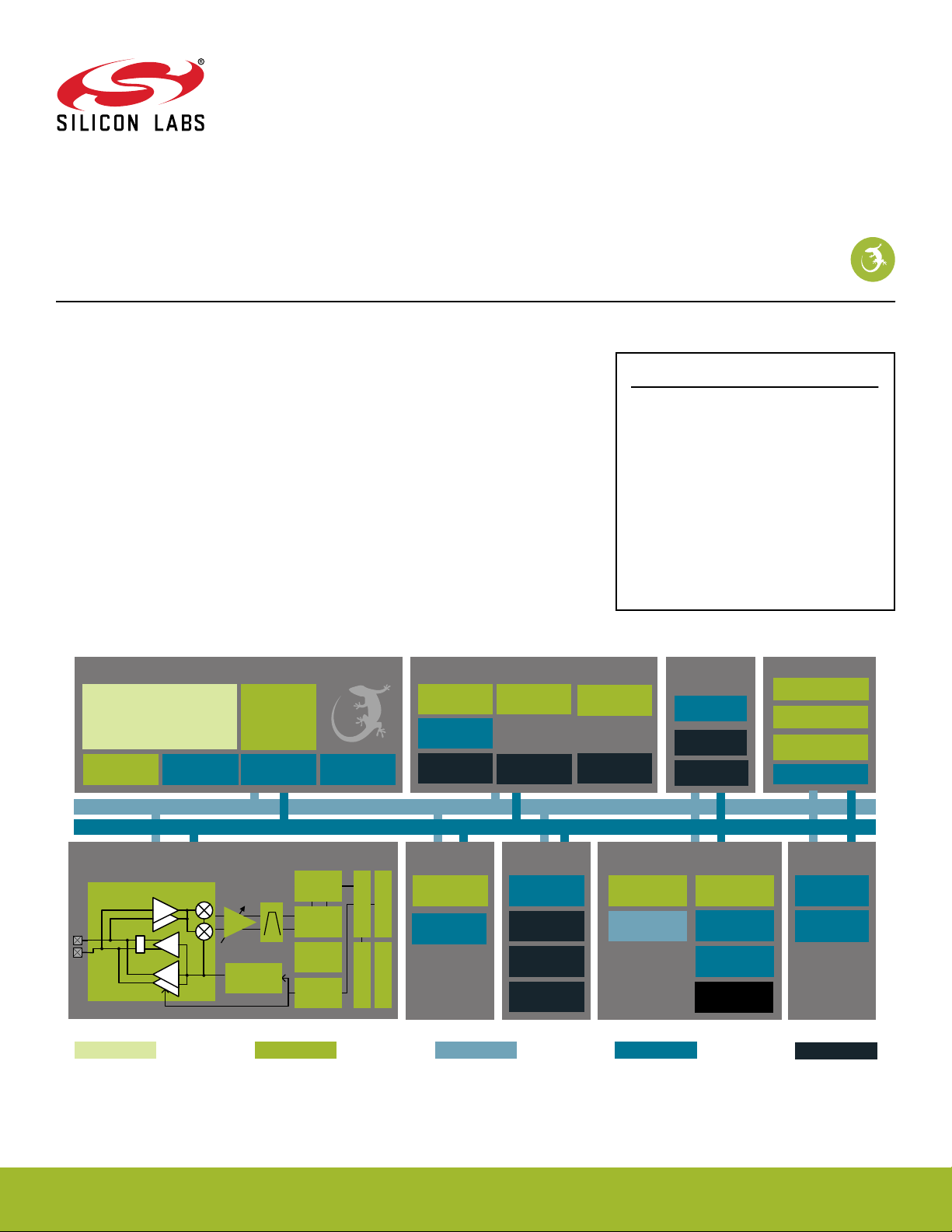
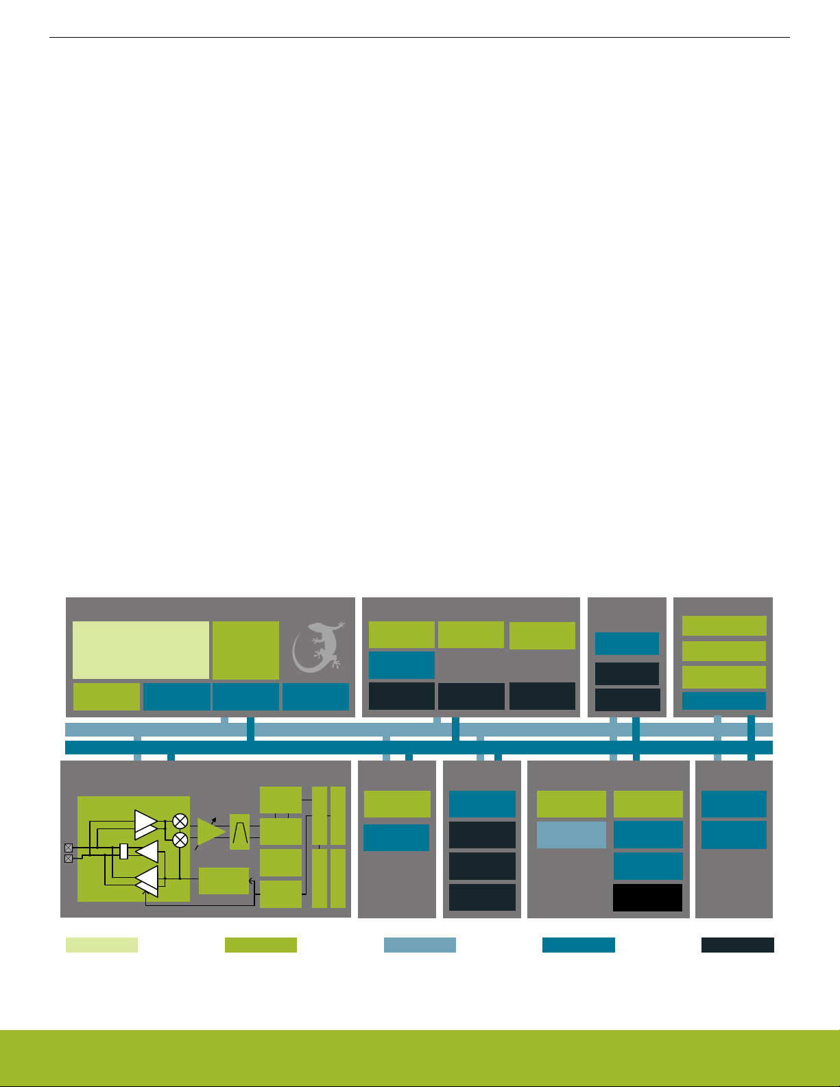
2.2 Block Diagrams
The block diagram for the EFR32xG21 System-On-Chip series is shown in (Figure 2.1 EFR32xG21 System-On-Chip Block Diagram on
page 26).
Core / Memory
ARM Cortex
TM
M33 processor
with DSP extensions,
FPU and Trust Zone
ETM Debug Interface RAM Memory
Flash Program
Memory
Radio Transceiver
RF Frontend
LNA
PA
PA
I
Q
PGA
Frequency
Synth
DEMOD
IFADC
AGC
MOD
LDMA
Controller
FRC
CRC
HF Crystal
Oscillator
EM23 HF RC
Oscillator
LF Crystal
Oscillator
32-bit bus
Peripheral Reflex System
Serial
Interfaces
USART
BUFC
RAC
2
I
C
Clock Management
HF
RC Oscillator
Ultra LF RC
Oscillator
I/O Ports Analog I/F
External
Interrupts
General
Purpose I/O
Pin Reset
Pin Wakeup
Fast Startup
RC Oscillator
LF
RC Oscillator
Timer/Counter
Low Energy Timer
Timers and Triggers
Energy
Management
Voltage
Regulator
Brown-Out
Detector
Power-On Reset
Protocol Timer
Watchdog Timer
Real Time
Capture Counter
Back-Up Real
Time Counter
Security
Crypto Acceleration
True Random
Number Generator
Secure Debug
Authentication
Secure Element
iADC
Analog
Comparator
Lowest power mode with peripheral operational:
EM3—StopEM2—Deep SleepEM1—SleepEM0—Active
EM4—Shutoff
Figure 2.1. EFR32xG21 System-On-Chip Block Diagram
silabs.com | Building a more connected world. Rev. 0.4 | 26
Page 27

Reference Manual
System Overview
2.3 MCU Features overview
• ARM Cortex-M33 CPU platform
• High Performance 32-bit processor @ up to 80 MHz
• DSP instruction support and floating-point unit
• Memory Protection Unit
• Wake-up Interrupt Controller
• Flexible Energy Management System
• 5 Energy Modes from EM0 to EM4 provide flexibility between higher performance and low power
• Power routing configurations including DCDC control
• Voltage Monitoring and Brown Out Detection
• State Retention
• Up to 1024 kB Flash
• Read-while-write support
• Up to 96 kB RAM
• Up to 20 General Purpose I/O pins
• Configurable push-pull, open-drain, pull-up/down, input filter, slew rate
• Configurable peripheral I/O locations
• 16 asynchronous external interrupts
• Output state retention and wake-up from Shutoff Mode
• 8 Channel DMA Controller
• Alternate/primary descriptors with scatter-gather/ping-pong operation
• 16 Channel Peripheral Reflex System (PRS)
• Autonomous inter-peripheral signaling enables smart operation in low energy modes
• 12 asynchronous channels with configurable logic functionality
• 4 synchronous channels for high-speed signalling between TIMER and IADC
• Advanced Encryption Standard Accelerator (AES)
• AES encryption / decryption, with 128 or 256 bit keys
• Multiple AES modes of operation, including Counter (CTR), Electronic CodeBook (ECB), Cipher Block Chaining (CBC), Counter
mode with CBC-MAC (CCM), and Cipher-based Message Authentication Code (CMAC).
• Accelerated SHA-1 and SHA-2 (SHA-224 / SHA-256)
• Accelerated Elliptic Curve Cryptography (ECC), with binary or prime fields
• Flexible 256-bit ALU and sequencer
• General Purpose Cyclic Redundancy Check (GPCRC)
• Programmable 16-bit polynomial, fixed 32-bit polynomial
• The GPCRC module is in addition to the radio CRC
• Communication interfaces
• 3 × Universal Synchronous/Asynchronous Receiver/Transmitter (USART)
• UART/SPI/SmartCard (ISO 7816)/IrDA/I2S
• Triple buffered full/half-duplex operation
• Hardware flow control
• 4-16 data bits
•
2 × I2C Interface (I2C) with SMBus support
• Address recognition in EM3 Stop Mode
silabs.com | Building a more connected world. Rev. 0.4 | 27
Page 28

• Timers/Counters
• 2 × 16-bit Timer/Counter (TIMER)
• Up to 3 Compare/Capture/PWM channels
• Dead-Time Insertion
• 32-bit Timer/Counter (TIMER)
• Up to 3 Compare/Capture/PWM channels
• 24-bit Low Energy Timer (LETIMER)
• 32-bit Ultra Low Energy Backup Real Time Counter (BURTC) for periodic wake-up from any Energy Mode
• 32-bit Real-Time Capture Counter (RTCC)
• 32-bit Back-Up Real-Time Counter (BURTC)
• 2 × Watchdog Timers (WDOG)
• Ultra low power precision analog peripherals
• 12-bit 1 Msps Incremental Analog to Digital Converter (IADC)
• Single ended or differential operation
• Conversion tailgating for predictable latency
• 2 × Analog Comparator (ACMP)
• Programmable speed/current
• Capacitive sensing
• Analog Bus (ABUS)
• Ultra efficient Power-on Reset (POR) and Brown-Out Detector (BOD)
• Debug Interface
• 4-pin Joint Test Action Group (JTAG) interface
• 2-pin serial-wire debug (SWD) interface
Reference Manual
System Overview
silabs.com | Building a more connected world. Rev. 0.4 | 28
Page 29

2.4 Oscillators and Clocks
EFR32xG21 has seven different oscillators integrated, as shown in Table 2.1 EFR32xG21 Oscillators on page 29.
Table 2.1. EFR32xG21 Oscillators
Reference Manual
System Overview
Oscillator Frequency Optional? External
Description
components
HFXO 38 MHz - 40 MHz No Crystal High accuracy, low jitter high frequency crystal oscillator. Tun-
able crystal loading capacitors are fully integrated. The HFXO
is required for all types of RF communication to be active.
HFRCO 1 MHz - 80 MHz Yes - Medium accuracy RC oscillator, typically used for timing dur-
ing startup of the HFXO and as a clock source as long as no
RF communication is active. In EM0/1 energy modes, the
HFRCO can be used in conjunction with the DPLL.
FSRCO 20 MHz No - Fast startup RC oscillator.
HFRCOEM23 1 MHz - 40 MHz Yes - Medium accuracy RC oscillator available in EM2 and EM3,
typically used as a clock source for the Analog to Digital Converter or Debug Trace.
LFRCO 32.768 kHz Yes - Medium accuracy frequency reference typically used for medi-
um accuracy RTCC timing.
LFXO 32.768 kHz Yes Crystal High accuracy frequency reference typically used for high ac-
curacy RTCC timing. Tunable crystal loading capacitors are
fully integrated.
ULFRCO 1000 Hz No - Ultra low frequency oscillator typically used for the watchdog
timer.
The RC oscillators can be calibrated against either of the crystal oscillators in order to compensate for temperature and voltage supply
variations. Hardware support is included to measure the frequency of various oscillators against each other.
Oscillator and clock management is available through the Clock Management Unit (CMU), see section 8. CMU - Clock Management
Unit for details.
2.5 RF Frequency Synthesizer
The Fractional-N RF Frequency Synthesizer (SYNTH) provides a low phase noise LO signal to be used in both receive and transmit
modes.
The capabilities of the SYNTH include:
• High performance, low phase noise
• Fast frequency settling
• Fast and fully automated calibration
• Sub 100 Hz frequency resolution across the supported frequency bands
2.6 Modulation Modes
EFR32xG21 supports a wide range of modulation modes in transmit and receive:
• 2-FSK, 2-GFSK, 4-FSK, 4-GFSK, MSK, GMSK, O-QPSK with half-sine shaping, ASK / OOK, DBPSK TX
• NRZ or Manchester support
• UART mode over air for legacy protocols
• Baudrates ranging from below 100 Baud/s to 2 MBaud/s, allowing data rates up to 4 MBit/s
• Configurable frequency deviation
• Configurable Direct Sequence Spread Spectrum (DSSS), with spread sequences up to 32 chips encoding up to 4 information bits
• Configurable 4-FSK symbol encoding
silabs.com | Building a more connected world. Rev. 0.4 | 29
Page 30

Reference Manual
System Overview
2.7 Transmit Mode
In transmit mode EFR32xG21 performs the following functionality:
• Automatic PA power ramping during the start and end of a frame transmit
• Programmable output power
• Optional preamble and synchronization word insertion
• Accurate transmit frame timing to support time synchronized radio protocols
• Optional Carrier Sense Multiple Access - Collision Avoidance (CSMA-CA) or Listen Before Talk (LBT) hardware support
• Integrated transmit test modes, as described in 2.17 RF Test Modes
2.8 Receive Mode
In receive mode EFR32xG21 performs the following functionality:
• A single-ended (2.4 GHz) LNA amplifies the input RF signal. The amplified signal is then mixed to a low-IF signal through the quadrature down-coversion mixer. Further signal filtering is performed before conversion to a digital signal through the I/Q ADC.
• Digitally configurable receiver bandwidth from 100 Hz to 2.5 MHz
• Timing recovery on received data, including simultaneous support for two different frame synchronization words
• Automatic frequency offset compensation, to compensate for carrier frequency offset between the transmitter and receiver
• Support for a wide range of modulation formats as described in section 2.6 Modulation Modes
2.9 Data Buffering
EFR32xG21 supports buffered transmit and receive modes through its buffer controller (BUFC), with four individually configurable buffers. The BUFC uses the system RAM as storage, and each buffer can be individually configured with parameters such as:
• Buffer size
• Buffer interrupt thresholds
• Buffer RAM location
• Overflow and underflow detection
In receive mode, data following frame synchronization is moved directly from the demodulator to the buffer storage.
In transmit mode, data following the inserted preamble and synchronization word is moved directly from the buffer storage to the modulator.
2.10 Unbuffered Data Transfer
For most system designs it is recommended to use the data buffering within EFR32xG21 to provide a convenient user interface.
In cases where data buffering within EFR32xG21 is not desired, it is possible to set up direct unbuffered data transfers using a singlepin or two-pin interface on EFR32xG21. A bit clock output is provided on the Serial Clock (SC) output pin, and a serial bitstream is
provided to EFR32xG21 in a transmit mode and from EFR32xG21 in a receive mode.
In unbuffered data transfer modes the hardware support provided by EFR32xG21 to perform preamble and frame synchronization insertion in transmit mode and detection in receive mode can still optionally be used.
2.11 Frame Format Support
EFR32xG21 has an extensive support for frame handling in transmit and receive modes, which allows effective handling of even advanced protocols. The frame format support is controlled by the Frame Controller (FRC). The support includes:
• Preamble and frame synchronization inserted into transmitted frames
• Full frame synchronization of received frames
• Simple address matching of received frames in hardware, further configurable address and frame filtering supported through sequencer
• Support for variable length frames
• Automated CRC calculation and verification
• Configurable bit ordering, with the most or least significant bit transmitted and received first
silabs.com | Building a more connected world. Rev. 0.4 | 30
Page 31

Reference Manual
System Overview
2.12 Hardware CRC Support
EFR32xG21 supports a configurable CRC generation in transmit and verification in receive mode:
• 8, 16, 24 or 32 bit CRC value
• Configurable polynomial and initialization value
• Optional inversion of CRC value over air
• Configurable CRC byte ordering
• Support for multiple CRC values calculated and verified per transmitted or received frame
• The CRC module is typically controlled by the Frame Controller (FRC) for in-line operations in transmit and receive modes. Alternatively, the CRC module may be accessed directly from software to calculate and verify CRC data.
2.13 Convolutional Encoding / Decoding
EFR32xG21 includes hardware support for convolutional encoding and decoding, for forward error correction (FEC). This feature is performed by the Frame Controller (FRC) module:
• Constraint length configurable up to 7, for the highest robustness
• Configurable puncturing, to achieve rates between 1/2 rate and full rate
• Configurable soft decision or hard decision decoding
• Convolutional coding may be used together with the symbol interleaver to improve robustness against burst errors
2.14 Binary Block Encoding / Decoding
EFR32xG21 includes hardware support for binary block encoding and decoding, both performed real-time in the the transmit and receive path. This is performed in the Frame Controller (FRC) module:
The block coding works on blocks of up to 16 bits of data and adds parity bits to be capable of single or multiple bit corrections by the
receiver.
• One or more parity bits can be added and verified
• Bit error correction
• Lookup-codes can be used to implement virtually any block coding scheme
silabs.com | Building a more connected world. Rev. 0.4 | 31
Page 32

Reference Manual
System Overview
2.15 Data Encryption and Authentication
EFR32xG21 has hardware support for AES encryption, decryption and authentication modes. These security operations can be performed on data in RAM or any data buffer, without further CPU intervention. The key size is 128 bits.
AES modes of operations directly supported by the EFR32xG21 hardware are listed in Table 2.2 AES modes of operation with hard-
ware support on page 32. In addition to these modes, other modes can also be implemented by using combinations of modes. For
example, the CCM mode can be implemented using the CTR and CBC-MAC modes in combination.
Table 2.2. AES modes of operation with hardware support
AES Mode Encryption / Decryption Authentication Comment
ECB Yes - Electronic Code Book
CTR Yes - Counter mode
CCM Yes Yes Counter with CBC-MAC
CCM* Yes Yes CCM with encryption-only and
integrity-only capabilities
GCM Yes Yes Galois Counter Mode
CBC Yes - Cipher Block Chaining
CBC-MAC - Yes Cipher Block Chaining, Mes-
sage Authentication Code
CMAC - Yes Cipher-basec MAC
CFB Yes - Cipher Feedback
OFB Yes - Output Feedback
The Cryptographic Acceleration module can operate directly on data buffers provided by the buffer controller (BUFC) module. It is also
possible to provide data directly from the embedded Cortex-M33 or via DMA.
silabs.com | Building a more connected world. Rev. 0.4 | 32
Page 33

2.16 Timers
EFR32xG21 includes multiple timers, as can be seen from Table 2.3 EFR32xG21 Timers Overview on page 33.
Table 2.3. EFR32xG21 Timers Overview
Timer Number of instances Typical clock source Overview
Reference Manual
System Overview
RTCC 1 Low frequency (LFXO or
LFRCO)
BURTC 1 Low frequency (LFXO or
LFRCO)
TIMER 3 High frequency (HFXO or
HFRCO)
Systick timer 1 High frequency (HFXO or
HFRCO)
WDOG 1 Low frequency (HCLK/1024,
LFXO, LFRCO or ULFRCO)
LETIMER 1 Low frequency (LFXO, LFRCO
or ULFRCO)
32 bit Real Time Counter and
Compare, typically used to accurately time inactive periods in
the radio communication protocol and enable wakeup on compare match.
32 bit Backup Real Time Counter that operates down to EM4.
16 or 32 bit general purpose
timer. (See configuration summary in datasheet for timer configration details.
24 bit systick timer integrated in
the Cortex-M33. Typically used
as an Operating System timer.
Watch dog timer. Once enabled,
this module must be periodically
accessed. If not, this is considered an error and the
EFR32xG21 is reset in order to
recover the system.
Low energy general purpose
timer.
PROTIMER 1 High frequency (HFXO or
HFRCO)
Protocol Timer, typically used
by the RF protocol Stack.
Advanced interconnect features allows synchronization between timers. This includes:
• Start / stop any high frequency timer synchronized with the RTCC
• Trigger RSM state transitions based on compare timer compare match, for instance to provide clock cycle accuracy on frame transmit timing
2.17 RF Test Modes
EFR32xG21 supports a wide range of RF test modes typically used for characterization and regulation compliance testing, including:
• Unmodulated carrier transmit
• Modulated carrier transmit, with internal configurable pseudo random data generator
• Continuous data reception for Bit Error Rate (BER) measurements
• Storing of raw receiver data to RAM
• Transmit of raw frequency data from RAM
silabs.com | Building a more connected world. Rev. 0.4 | 33
Page 34

3. System Processor
43210
CM33 Core
Reference Manual
System Processor
Quick Facts
What?
The EFR32xG21 features the industry leading Cortex-M33 CPU from ARM.
Why?
The ARM Cortex-M33 is designed for exceptionally
short response time, high code density, and high 32bit throughput while maintaining a strict cost and
power consumption budget.
3.1 Introduction
32-bit ALU
Hardware divider
Memory Protection Unit DSP extensions
Trust Zone
Instruction Interface Data Interface
NVIC Interface
Single cycle
32-bit multiplier
Floating-Point Unit
Thumb & Thumb-2
Decode
How?
Combined with the ultra low energy peripherals
available in EFR32xG21 devices, the Cortex-M33
processor's Harvard architecture, 3 stage pipeline,
single cycle instructions, Thumb-2 instruction set
support, and fast interrupt handling make it perfect
for 8-bit, 16-bit, and 32-bit applications.
The ARM Cortex-M33 32-bit RISC processor provides outstanding computational performance and exceptional system response to interrupts while meeting low cost requirements and low power consumption.
The ARM Cortex-M33 implemented is revision r0p1.
silabs.com | Building a more connected world. Rev. 0.4 | 34
Page 35

Reference Manual
System Processor
3.2 Features
• Harvard architecture
• Separate data and program memory buses (No memory bottleneck as in a single bus system)
• 3-stage pipeline
• Thumb-2 instruction set
• Enhanced levels of performance, energy efficiency, and code density
• Single cycle multiply and hardware divide instructions
• 32-bit multiplication in a single cycle
• Signed and unsigned divide operations between 2 and 12 cycles
• 1.5 DMIPS/MHz
• Trust Zone
• Independent Secure and Privileged states
• Accelerated context switching
• 16 Region MPU
• 24-bit System Tick Timer for Real Time OS
• Excellent 32-bit migration choice for 8/16 bit architecture based designs
• Simplified stack-based programmer's model is compatible with traditional ARM architecture and retains the programming simplicity of legacy 8-bit and 16-bit architectures
• Aligned or unaligned data storage and access
• Contiguous storage of data requiring different byte lengths
• Data access in a single core access cycle
• Integrated power modes
• Sleep Now mode for immediate transfer to low power state
• Sleep on Exit mode for entry into low power state after the servicing of an interrupt
• Ability to extend power savings to other system components
• Optimized for low latency, nested interrupts
3.3 Functional Description
For a full functional description of the ARM Cortex-M33 implementation in the EFR32xG21 family, the reader is referred to the ARM
Cortex-M33 documentation.
silabs.com | Building a more connected world. Rev. 0.4 | 35
Page 36

Reference Manual
System Processor
3.3.1 Interrupt Operation
Module Cortex-M NVIC
IEN[n]
Register
Write
Interrupt
condition
set clear
IF[n]
IRQ
Figure 3.1. Interrupt Operation
The interrupt request (IRQ) lines are connected to the Cortex-M33. Each of these lines (shown in 3.3.3 Interrupt Request lines (IRQ)) is
connected to one or more interrupt flags in one or more modules. The interrupt flags are set by hardware on an interrupt condition. It is
also possible to set/clear the interrupt flags through the IF registers. When setting or clearing and interrupt through the IF register use of
the IF_SET or IF_CLEAR bit operation registers is recommended.
SETENA[n]/CLRENA[n]
Active interrupt
set clear
SETPEND[n]/CLRPEND[n]
Software generated interrupt
Interrupt
request
Each interrupt flag is then qualified with its own interrupt enable bit (IEN register), before being OR'ed with the other interrupt flags to
generate the IRQ. A high IRQ line will set the corresponding pending bit (can also be set/cleared with the SETPEND/CLRPEND bits in
ISPRn/ICPRn) in the Cortex-M33 NVIC. The pending bit is then qualified with an enable bit (set/cleared with SETENA/CLRENA bits in
ISERn/ICERn) before generating an interrupt request to the core. Figure 3.1 Interrupt Operation on page 36 illustrates the interrupt system. For more information on how the interrupts are handled inside the Cortex-M33, the reader is referred to the EFR32 Cortex-M33
Reference Manual.
3.3.1.1 Avoiding Extraneous Interrupts
There can be latencies in the system such that clearing an interrupt flag could take longer than leaving an Interrupt Service Routine
(ISR). This can lead to the ISR being re-entered as the interrupt flag has yet to clear immediately after leaving the ISR. To avoid this,
when clearing an interrupt flag at the end of an ISR, the user should execute ARM's Data Synchronization Barrier (DSB) instruction.
Another approach is to clear the interrupt flag immediately after identifying the interrupt source and then service the interrupt as shown
in the pseudo-code below. The ISR typically is sufficiently long to more than cover the few cycles it may take to clear the interrupt status, and also allows the status to be checked for further interrupts before exiting the ISR.
irqXServiceRoutine() {
do {
clearIrqXStatus();
serviceIrqX();
} while(irqXStatusIsActive());
}
3.3.2 TrustZone
The Cortex-M33 implements ARM TrustZone which provides the ability to restrict access to peripherals and memory regions based on
the CPU security attribute. TrustZone works in combination which the MPU which controls privileged/unprivileged execution of code to
provide a full security solution. The Security Management Unit (SMU) is used to configure access restrictions in the various modes.
Refer to 10. SMU - Security Management Unit for more information.
For information about TrustZone features in the core or information on TrustZone specific instructions please see the EFR32 CortexM33 Reference Manual provided by ARM
silabs.com | Building a more connected world. Rev. 0.4 | 36
Page 37

3.3.3 Interrupt Request lines (IRQ)
This table shows all IRQ's for the system processor. M33 High Speed interrupts are indicated by an '*'.
See the individual peripheral chapters for more information on interrupt function.
IRQ # Name Source(s)
0* SETAMPERHOST SE.tamper_hostirq
1* SEMBRX SE.mb_rxint
2* SEMBTX SE.mb_txint
3* SMU_SECURE SMU.SECURE
4* SMU_PRIVILEGED SMU.PRIVILEGED
5* EMU EMU.MAIN
6* TIMER0 TIMER0.MAIN
7* TIMER1 TIMER1.MAIN
8* TIMER2 TIMER2.MAIN
9* TIMER3 TIMER3.MAIN
Reference Manual
System Processor
10* RTCC RTCC.MAIN
11* USART0_RX USART0.RX
12* USART0_TX USART0.TX
13* USART1_RX USART1.RX
14* USART1_TX USART1.TX
15* USART2_RX USART2.RX
16* USART2_TX USART2.TX
17* ICACHE0 ICACHE0.MAIN
18* BURTC BURTC.MAIN
19* LETIMER0 LETIMER0.MAIN
20* SYSCFG SYSCFG.MAIN
21* LDMA LDMA.MAIN
22* LFXO LFXO.MAIN
23* LFRCO LFRCO.MAIN
24* ULFRCO ULFRCO.MAIN
25* GPIO_ODD GPIO.ODD
26* GPIO_EVEN GPIO.EVEN
27* I2C0 I2C0.irq
28* I2C1 I2C1.irq
29* EMUDG EMU.DG
30* EMUSE EMU.SE
31* AGC AGC.MAIN
32* BUFC BUFC.MAIN
33* FRC_PRI FRC.PRI
silabs.com | Building a more connected world. Rev. 0.4 | 37
Page 38

IRQ # Name Source(s)
34* FRC FRC.MAIN
35* MODEM MODEM.MAIN
36* PROTIMER PROTIMER.MAIN
37* RAC_RSM RAC.RSM
38* RAC_SEQ RAC.SEQ
39* PRORTC PRORTC.MAIN
40* SYNTH SYNTH.MAIN
41* ACMP0 ACMP0.MAIN
42* ACMP1 ACMP1.MAIN
43* WDOG0 WDOG0.MAIN
44* WDOG1 WDOG1.MAIN
45* HFXO00 HFXO0.MAIN
46* HFRCO0 HFRCO0.MAIN
Reference Manual
System Processor
47* HFRCOEM23 HFRCOEM23.MAIN
48* CMU CMU.MAIN
49* AES RADIOAES.MAIN
50* IADC IADC0.MAIN
51* MSC MSC.irq_imem
52* DPLL0 DPLL0.MAIN
53* SW0 SYSCFG.SW0
54* SW1 SYSCFG.SW1
55* SW2 SYSCFG.SW2
56* SW3 SYSCFG.SW3
57* KERNEL0
58* KERNEL1
59* M33CTI0 CORE.CTI0
60* M33CTI1 CORE.CTI1
silabs.com | Building a more connected world. Rev. 0.4 | 38
Page 39

4. Memory and Bus System
43210
ARM Cortex-M
DMA Controller
Flash
RAM
Peripherals
Reference Manual
Memory and Bus System
Quick Facts
What?
A low latency memory system including low energy
Flash and RAM with data retention which makes the
low energy modes attractive.
Why?
RAM retention reduces the need for storing data in
Flash and enables frequent use of the ultra low energy modes EM2 and EM3.
How?
Low energy and non-volatile Flash memory stores
program and application data in all energy modes
and can easily be reprogrammed in system. Low
leakage RAM with data retention in EM0 to EM3 removes the data restore time penalty, and the DMA
ensures fast autonomous transfers with predictable
response time.
4.1 Introduction
The EFR32xG21 contains a set of AMBA buses which move data between peripherals, memory, and the CPU. All memories and register interfaces are memory mapped into a unified address space.
silabs.com | Building a more connected world. Rev. 0.4 | 39
Page 40

Reference Manual
Memory and Bus System
4.2 Functional Description
The internal memory segments of the Cortex-M33 are mapped into the system memory map as shown by Figure 4.1 System Address
Space with Core and Code Space Listing on page 40.
Figure 4.1. System Address Space with Core and Code Space Listing
Flash for the main program memory (CODE) is located at address 0x00000000 in the memory map of the EFR32xG21.
SRAM for the main data memory (RAM) is located at address 0x20000000 in the memory map of the EFR32xG21. When running code
located in RAM, the Cortex-M33 uses the System bus interface to fetch instructions. This results in reduced performance as the CortexM33 accesses stack, other data in SRAM and peripherals using the System bus interface.
The Sequencer RAM (SEQRAM) is located at address 0xA0000000 and is used by the Sequencer for both instructions and data. This
RAM is also available for general use if not required by the RF subsystem.
silabs.com | Building a more connected world. Rev. 0.4 | 40
Page 41

Reference Manual
Memory and Bus System
4.2.1 Bus Matrix
A multilayer AMBA AHB bus matrix connects the master bus interfaces to the AHB slaves. The bus matrix allows several AHB slaves to
be accessed simultaneously. An AMBA APB interface is used for the peripherals, which are accessed through an AHB-to-APB bridge
connected to the AHB bus matrix.
The CPU has two AHB bus masters (Code and System) so that it may retrieve instructions and data in parallel. The Code master is
used to access all memory below address 0x20000000 and the System master access addresses 0x20000000 and above.
Cortex-M
LDMA
Code
System
AHB Multilayer
Bus Matrix
Flash
RAM (DMEM)
SEQRAM
SE_MAILBOX
AHB/APB
Bridge
(High
Frequency)
AHB/APB
Bridge
(Low
Frequency)
Peripheral a
Peripheral n
Peripheral m
Peripheral z
Figure 4.2. EFR32xG21 Bus System
4.2.1.1 Arbitration
The Bus Matrix uses a round-robin arbitration algorithm which enables high throughput and low latency, while starvation of simultaneous accesses to the same bus slave are eliminated. Round-robin does not assign a fixed priority to each bus master. The arbiter does
not insert any bus wait-states during peak interaction. However, one wait state is inserted for master accesses occurring after a prolonged inactive time. This wait state allows for increased power efficiency during master idle time.
4.2.1.2 Bus Faults
System accesses from the core can receive a bus fault in the following condition(s):
• The core attempts to access an address that is not assigned to any peripheral or other system device. These faults can be enabled
or disabled by setting the ADDRFAULTEN bit in the SYSCFG_CTRL register.
• The core attempts to access a peripheral register that is LOCKED.
• The core attempts to access a peripheral or system device that has its clock disabled. The radio subsystem is the only peripheral
with an independent bus clock that can generate a fault of this type. This fault can be enabled or disabled by setting the ADDRFAULTEN bit in the SYSCFG_CTRL register.
• System RAM controller or RADIO RAM controller detects a 2bit ECC error. These faults can be enabled or disabled by setting the
RAMECCERRFAULTEN bit in the SYSCFG_CTRL register
• Registers with synchronization requirements may generate bus faults if accessed incorrectly. See 4.2.4.4 Peripheral Access Per-
formance for more details on register access types. In particular the following actions can cause bus faults:
• Config register written while peripheral enabled.
• Sync register written while peripheral disabled
• LfSync register written while a previous write is pending
• Peripheral disabled while any LfSync write is pending
In addition to any condition-specific bus fault control bits, the bus fault interrupt itself can be enabled or disabled in the same way as all
other internal core interrupts.
silabs.com | Building a more connected world. Rev. 0.4 | 41
Page 42

Reference Manual
Memory and Bus System
4.2.2 Flash
The Flash retains data in any state and typically stores the application code and special user data. The Flash memory is typically programmed through the debug interface, but can also be erased and written to from software.
• Up to 1024 kB of memory
• Page size of 8 KB (minimum erase unit)
• Minimum 10k erase cycles endurance
• Greater than 10 years data retention at 85°C
• Lock registers for memory protection
• Data retention in any state
4.2.3 SRAM
The primary task of the SRAM memory is to store application data. Additionally, it is possible to execute instructions from SRAM, and
the DMA may be set up to transfer data between the SRAM, Flash and peripherals.
The device contains several blocks of SRAM for various purposes including general data memory (RAM) and various RF subsystem
rams (SEQRAM, FRCRAM). For more detailed information see 6. MSC - Memory System Controller .
• Up to 96 kB of memory (RAM)
• RAM blocks may be powered down when not in use
• Data retention of the entire memory in EM2 to EM3
4.2.4 Peripherals
The peripherals are mapped into the peripheral memory segment, each with a fixed size address range shown in the 4.2.4.1 Peripheral
Map
silabs.com | Building a more connected world. Rev. 0.4 | 42
Page 43

Reference Manual
Memory and Bus System
4.2.4.1 Peripheral Map
This table shows the address range for each peripheral. In addition it shows the lowest energy mode in which the peripheral is powered. Note that EM3 is defined as EM2 with all clocks disabled. Therefore all peripherals powered in EM2 are also powered in EM3 but
may not function if they require a running clock.
See the individual peripheral chapters for more information on low power operation.
Address Range Module Name Power Domain
0x40004000 - 0x40007FFF EMU EM2.B
0x40008000 - 0x4000BFFF CMU EM2.B
0x4000C000 - 0x4000FFFF HFXO0 EM1
0x40010000 - 0x40013FFF HFRCO0 EM1
0x40018000 - 0x4001BFFF FSRCO EM4
0x4001C000 - 0x4001FFFF DPLL0 EM1
0x40020000 - 0x40023FFF LFXO EM4
0x40024000 - 0x40027FFF LFRCO EM4
0x40028000 - 0x4002BFFF ULFRCO EM4
0x40030000 - 0x40033FFF MSC EM1
0x40034000 - 0x40037FFF ICACHE0 EM1
0x40038000 - 0x4003BFFF PRS EM2.B
0x4003C000 - 0x4003FFFF GPIO EM2.A
0x40040000 - 0x40043FFF LDMA EM1
0x40044000 - 0x40047FFF LDMAXBAR EM1
0x40048000 - 0x4004BFFF TIMER0 EM1
0x4004C000 - 0x4004FFFF TIMER1 EM1
0x40050000 - 0x40053FFF TIMER2 EM1
0x40054000 - 0x40057FFF TIMER3 EM1
0x40058000 - 0x4005BFFF USART0 EM1
0x4005C000 - 0x4005FFFF USART1 EM1
0x40060000 - 0x40063FFF USART2 EM1
0x40064000 - 0x40067FFF BURTC EM4
0x40068000 - 0x4006BFFF I2C1 EM1
0x40074000 - 0x40077FFF LVGD EM2.B
0x4007C000 - 0x4007FFFF SYSCFG EM1
0x40080000 - 0x40083FFF BURAM EM4
0x40088000 - 0x4008BFFF GPCRC EM1
0x44000000 - 0x44003FFF RADIOAES EM1
0x44004000 - 0x44007FFF BUFC EM1
0x44008000 - 0x4400BFFF SMU EM1
0x48000000 - 0x48003FFF RTCC EM2.A
0x4A000000 - 0x4A003FFF LETIMER0 EM2.B
silabs.com | Building a more connected world. Rev. 0.4 | 43
Page 44

Memory and Bus System
Address Range Module Name Power Domain
0x4A004000 - 0x4A007FFF IADC0 EM2.B
0x4A008000 - 0x4A00BFFF ACMP0 EM2.B
0x4A00C000 - 0x4A00FFFF ACMP1 EM2.B
0x4A010000 - 0x4A013FFF I2C0 EM2.B
0x4A014000 - 0x4A017FFF HFRCOEM23 EM2.B
0x4A018000 - 0x4A01BFFF WDOG0 EM2.B
0x4A01C000 - 0x4A01FFFF WDOG1 EM2.B
0x4A020000 - 0x4A023FFF AMUXCP0 EM2.B
0x4C000000 - 0x4C00007F SEMAILBOX EM1
0x50004000 - 0x50007FFF EMU_NS EM2.B
0x50008000 - 0x5000BFFF CMU_NS EM2.B
0x5000C000 - 0x5000FFFF HFXO0_NS EM1
0x50010000 - 0x50013FFF HFRCO0_NS EM1
Reference Manual
0x50018000 - 0x5001BFFF FSRCO_NS EM4
0x5001C000 - 0x5001FFFF DPLL0_NS EM1
0x50020000 - 0x50023FFF LFXO_NS EM4
0x50024000 - 0x50027FFF LFRCO_NS EM4
0x50028000 - 0x5002BFFF ULFRCO_NS EM4
0x50030000 - 0x50033FFF MSC_NS EM1
0x50034000 - 0x50037FFF ICACHE0_NS EM1
0x50038000 - 0x5003BFFF PRS_NS EM2.B
0x5003C000 - 0x5003FFFF GPIO_NS EM2.A
0x50040000 - 0x50043FFF LDMA_NS EM1
0x50044000 - 0x50047FFF LDMAXBAR_NS EM1
0x50048000 - 0x5004BFFF TIMER0_NS EM1
0x5004C000 - 0x5004FFFF TIMER1_NS EM1
0x50050000 - 0x50053FFF TIMER2_NS EM1
0x50054000 - 0x50057FFF TIMER3_NS EM1
0x50058000 - 0x5005BFFF USART0_NS EM1
0x5005C000 - 0x5005FFFF USART1_NS EM1
0x50060000 - 0x50063FFF USART2_NS EM1
0x50064000 - 0x50067FFF BURTC_NS EM4
0x50068000 - 0x5006BFFF I2C1_NS EM1
0x50074000 - 0x50077FFF LVGD_NS EM2.B
0x5007C000 - 0x5007FFFF SYSCFG_NS EM1
0x50080000 - 0x50083FFF BURAM_NS EM4
0x50088000 - 0x5008BFFF GPCRC_NS EM1
silabs.com | Building a more connected world. Rev. 0.4 | 44
Page 45

Memory and Bus System
Address Range Module Name Power Domain
0x54000000 - 0x54003FFF RADIOAES_NS EM1
0x54004000 - 0x54007FFF BUFC_NS EM1
0x54008000 - 0x5400BFFF SMU_NS EM1
0x58000000 - 0x58003FFF RTCC_NS EM2.A
0x5A000000 - 0x5A003FFF LETIMER0_NS EM2.B
0x5A004000 - 0x5A007FFF IADC0_NS EM2.B
0x5A008000 - 0x5A00BFFF ACMP0_NS EM2.B
0x5A00C000 - 0x5A00FFFF ACMP1_NS EM2.B
0x5A010000 - 0x5A013FFF I2C0_NS EM2.B
0x5A014000 - 0x5A017FFF HFRCOEM23_NS EM2.B
0x5A018000 - 0x5A01BFFF WDOG0_NS EM2.B
0x5A01C000 - 0x5A01FFFF WDOG1_NS EM2.B
0x5A020000 - 0x5A023FFF AMUXCP0_NS EM2.B
Reference Manual
0x5C000000 - 0x5C00007F SEMAILBOX_NS EM1
0xA8004000 - 0xA8007FFF FRC EM1
0xA800C000 - 0xA800FFFF AGC EM1
0xA8010000 - 0xA8013FFF RFCRC EM1
0xA8014000 - 0xA8017FFF MODEM EM1
0xA8018000 - 0xA801BFFF SYNTH EM1
0xA801C000 - 0xA801FFFF PROTIMER EM1
0xA8020000 - 0xA8023FFF RAC EM1
0xB8004000 - 0xB8007FFF FRC_NS EM1
0xB800C000 - 0xB800FFFF AGC_NS EM1
0xB8010000 - 0xB8013FFF RFCRC_NS EM1
0xB8014000 - 0xB8017FFF MODEM_NS EM1
0xB8018000 - 0xB801BFFF SYNTH_NS EM1
0xB801C000 - 0xB801FFFF PROTIMER_NS EM1
0xB8020000 - 0xB8023FFF RAC_NS EM1
4.2.4.2 Peripheral non-word access behavior
When writing to peripheral registers, all accesses are treated as 32-bit accesses. This means that writes to a register need to be large
enough to cover all bits of register, otherwise, any uncovered bits may become corrupted from the partial-word transfer. Thus, the safest practice is to always do 32-bit writes to peripheral registers.
When reading, there is generally no issue with partial word accesses, however, note that any read action (e.g. FIFO popping) will be
triggered regardless of whether the actual FIFO bit-field was included in the transfer size.
silabs.com | Building a more connected world. Rev. 0.4 | 45
Page 46

Reference Manual
Memory and Bus System
4.2.4.3 Peripheral Bit Set and Clear
The EFR32xG21 supports bit set, bit clear, and bit toggle access to most peripheral registers. The bit set and bit clear functionality (also
called Bit Access) enables modification of bit fields without the need to perform a read-modify-write. Also, the operation is contained
within a single bus access. Bit access registers and their addresses are shown in the register map for each peripheral. Peripherals with
no _SET, _CLR, or _TGL registers in the register map to not support these functions.
Each register with Bit Set functionality will have a _SET register. Whenever a bit in the SET register is written to a 1 the corresponding
bit in its target register is set. The SET register is located at TARGET + 0x1000 where TARGET is the address of the target register and
has the same name as the target register with '_SET' appended.
Each register with Bit Clear functionality will have a CLR register. Whenever a bit in the CLR register is written to a 1 the corresponding
bit in its target register is cleared. The CLR register is located at TARGET + 0x2000 where TARGET is the address of the target register
and has the same name as the target register with '_CLR' appended.
Each register with Bit Toggle functionality will have a TGL register. Whenever a bit in the TGL register is written to a 1 the corresponding bit in its target register is inverted. The TGL register is located at TARGET + 0x3000 where TARGET is the address of the target
register and has the same name as the target register with '_TGL' appended.
Note: It is possible to combine bit clear and bit set operations in order to arbitrarily modify multi-bit register fields without affecting other
fields in the same register. In this case, care should be taken to ensure that the field does not have intermediate values that can lead to
erroneous behavior. For example, if bit clear and bit set operations are used to change an analog tuning register field from 0x2 to 0x4
by clearing bit 1 and then setting bit 2, the field would take on a value of zero for short time. If the analog module is active at the time,
this could lead to undesired behavior.
4.2.4.4 Peripheral Access Performance
The Cortex-M33, DMA Controller, and peripherals run on clocks which can be pre-scaled separately. Clocks and pre-scaling are described in more detail in 8. CMU - Clock Management Unit. This section describes the access performance for a peripheral register based
on its frequency relative to the CPUCLK frequency and its access type. For this discussion, PERCLK refers to a selected peripheral's
clock frequency and CPUCLK refers to the core's clock frequency.
The type of each register in a peripheral is indicated in the 'Access' column of the peripherals register table. Register types are: ENABLE, CONFIG, SYNC, LFSYNC, and INTFLAG. If not type is listed then the register is a Generic register.
4.2.4.4.1 Generic Registers
Registers with no type listed are generic registers. They may be read or written to at any time. Access will not stall the CPU.
4.2.4.4.2 CONFIG Registers
CONFIG Registers contain configuration that does not change during peripheral operation.
CONFIG registers may only be written when a peripheral is disabled. Writing to a CONFIG register when a peripheral is enabled will
result in a BUSFAULT. CONFIG register writes will not stall the CPU.
CONFIG registers may be read at any time. Reads will not stall the CPU.
4.2.4.4.3 SYNC Registers
SYNC registers are used to communicate with running high-speed peripherals where PERCLK is expected to be either higher or marginally slower (within an order of magnitude) than CPUCLK. For example a timer running at 80Mhz when the core is at 40Mhz or at
10Mhz when the core is 80Mhz. In this case CPU stalls of several PERCLOCK cycles do not significantly impact overall system performance in most systems.
SYNC registers may only be written to when the peripheral is enabled. Writing to a SYNC register when a peripheral is disabled will
result in a BUSFAULT. A write will take several (2 - 3) PERCLK cycles to complete (take effect) during which time the entire module will
be in a pending state. If a SYNC register is written to while the peripheral is already in a pending state, the CPU is stalled until the
previous write finishes. If a SYNC register is written to while the peripheral is not in a pending state, the CPU is not stalled.
SYNC registers may be read at any time. If a SYNC register is read while the peripheral is disabled, the CPU is not stalled. If a SYNC
register is read while the peripheral is enabled, the CPU will be stalled for several (2 -3) PERCLK cycles while up to date values are
retrieved from the peripheral.
silabs.com | Building a more connected world. Rev. 0.4 | 46
Page 47

Reference Manual
Memory and Bus System
4.2.4.4.4 LFSYNC Registers
LFSYNC registers are used to communicate with running low frequency peripherals where PERCLK is expected to be much lower than
the CPU clock and synchronization delays may be long. For example, a LETIMER running at 32Khz when the core is at 80Mhz. In this
case CPU stalls of several PERCLOCK cycles represent a significant blockage of the CPU and need to be avoided whenever possible.
LFSYNC registers accommodate this by allowing the CPU to write the register and continue to do other work while the value is
synchronized.
Each LFSYNC register has a SYNCBUSY bit indicating if it is currently pending. Software should check the busy status bit before writing to an LFSYNC register. If a LFSYNC register is written to while it is in a pending state, a BUSFAULT will occur. A write will take will
take several (3 -4) PERCLK cycles to complete during which time the register will be in a pending state with the busy status bit set.
Software may use the busy status bit to determine when the write has taken effect.
LFSYNC registers may be read at any time. The CPU is never stalled on a read. Some LFSYNC registers are static, meaning the value
is not modified by hardware. If a static LFSYNC register is read while pending, the pending (recently written) data may be returned even
though it has not yet taken effect. Some LFSYNC registers are volatile, meaning the value may be modified by hardware. If a volatile
LFSYNC register is read, it will return the current value of the register, ignoring any pending (recently written) data that has not yet
taken effect.
4.2.4.4.5 ENABLE Registers
ENABLE registers contain the enable bit for a peripheral.
ENABLE registers may be written at any time. When the peripheral is enabled it takes some time for the enable to take effect during
which time the module is pending. Peripherals will be in the pending state for a few (2 - 3) PERCLK cycles when first enabled. Since the
clock source for the peripheral may not be running before the peripheral is enabled, the start up time for the clock source may increase
the pending time. See EFR32xG21 Wireless Gecko for more information on on-demand clock sources.
Disabling a high frequency module will stall the CPU until all pending SYNC writes have completed and any pending enable has completed. If the module is fully enabled and no SYNC writes are pending, the disable will be instantaneous. Disabling low frequency peripheral which a LFSYNC is pending will result in a bus fault. Disabling a low frequency peripherals while an enable is still pending
causes no CPU stall.
ENABLE registers may be read at any time.
4.2.4.4.6 INTFLAG Registers
INTFLAG registers contain interrupt flags. To set or clear an interrupt flag, the _SET or _CLR register alias must be used. Writing directly to the INTFLAG register will have no effect.
Note that for an interrupt to occur when a flag is set the IRQ must be enabled in the NVIC.
silabs.com | Building a more connected world. Rev. 0.4 | 47
Page 48

5. Radio Transceiver
43210
Reference Manual
Radio Transceiver
Quick Facts
What?
The Radio Transceiver provides access to transmit
and receive data, radio settings and control interface.
Why?
The Radio Transceiver enables the user to communicate using a wide range of data rates, modulation
and frame formats.
How?
Dynamic or fixed frame lengths, optional address
recognition, flexible CRC and crypto schemes
makes the EFR32 Series 2 perfectly suit any application using low or medium data rate radio communication.
silabs.com | Building a more connected world. Rev. 0.4 | 48
Page 49

Reference Manual
Radio Transceiver
5.1 Introduction
The Radio Transceiver of the EFR32 Series 2 enables the user to control a wide range of settings and options for tailoring radio operation precisely to the users need. It provides access to the transmit and receive data buffers and supports both dynamic and static frame
lengths, as well as automatic address filtering and CRC insertion/verification.
As seen in the Radio Overview illustration (Figure 5.1 Radio Overview on page 49), the radio consists of several modules all responsible for specific tasks. Please refer to the abbreviations section (Appendix 1. Abbreviations) for a comprehensive description of acronyms.
Radio Transceiver
IFADC
RFIN
LNA
IFADC
Demodulator
(DEMOD)
(BUFC)
Buffer Controller
MATCH / FILTER
RFOUT0
RFOUT1
PA0
PA1
Fractional-N
Frequency
Synthesizer
Automatic
Gain Control
(AGC)
Modulator
(MOD)
(FRC)
Frame Controller
(RAC)
Radio Controller
CRC
Figure 5.1. Radio Overview
During transmission (TX), the Radio Controller enables the SYNTH, Modulator and PA. The Modulator requests data from the Frame
Controller, which reads data from a buffer. Based upon modulation format and data to send, the Modulator manipulates the SYNTH to
output the correct frequency and phase. When the whole frame has been transmitted, the radio can automatically switch to receive
mode.
In receive mode (RX), the radio controller enables the LNA, SYNTH, Mixer, ADC and Demodulator. The Demodulator searches for valid
frames according to modulation format and data rate. If a frame is detected, the demodulated data is handed to the Frame Controller,
which stores the data in the Buffer. When the complete frame has been received (determined by the Frame Controller), it is possible to
either go to TX or stay in RX to search for a new frame.
The Radio Transceiver interface is accessible through software drivers provided by Silicon Labs.
silabs.com | Building a more connected world. Rev. 0.4 | 49
Page 50

6. MSC - Memory System Controller
43210
Reference Manual
MSC - Memory System Controller
Quick Facts
What?
The user can perform Flash memory read, read configuration, and write operations through the Memory
System Controller (MSC). SRAM operation may be
configured though System Configuration (SYSCFG).
01000101011011100110010101110010
01100111011110010010000001001101
01101001011000110111001001101111
00100000011100100111010101101100
01100101011100110010000001110100
01101000011001010010000001110111
01101111011100100110110001100100
00100000011011110110011000100000
01101100011011110111011100101101
01100101011011100110010101110010
01100111011110010010000001101101
01101001011000110111001001101111
01100011011011110110111001110100
01110010011011110110110001101100
01100101011100100010000001100100
01100101011100110110100101100111
01101110001000010100010101101110
Why?
The MSC allows the application code, user data,
and flash lock bits to be stored in non-volatile Flash
memory. Certain memory system functions, such as
program memory wait-states are also configured
from the MSC peripheral register interface, giving
the developer the ability to dynamically customize
the memory system performance, security level, energy consumption and error handling capabilities to
the requirements at hand.
How?
The MSC integrates a low-energy Flash IP with a
charge pump, enabling minimum energy consumption while eliminating the need for external programming voltage to erase the memory. An easy to use
write and erase interface is supported by an internal,
fixed-frequency oscillator and autonomous flash timing and control reduces software complexity while
not using other timer resources.
A highly efficient low energy instruction cache reduces the number of flash reads significantly, thus
saving energy. Performance is also improved when
wait-states are used, since many of the wait-states
are eliminated. Built-in performance counters can be
used to measure the efficiency of the instruction
cache.
Instruction prefetcher improves program execution
performance by reducing the number of wait-state
cycles needed.
6.1 Introduction
The Memory System Controller (MSC) is the program memory unit of the EFR32xG21 microcontroller. The flash memory is readable
and writable from both the Cortex-M33 and DMA. The flash memory is divided into two blocks: the main block and the information
block. Program code is normally written to the main block. The information block is available for special user data. There is also a readonly page in the information block containing system and device calibration data. Flash read and write operations are supported in the
energy modes EM0 and EM1.
silabs.com | Building a more connected world. Rev. 0.4 | 50
Page 51

6.2 Features
• AHB read interface
• Scalable access performance to optimize the Cortex-M33 code interface
• Advanced energy optimization functionality
• Conditional branch target prefetch suppression
• Cortex-M33 disfolding of if-then (IT) blocks
• Instruction Cache
• Instruction Prefetch
• DMA read support in EM0 and EM1
• Command and status interface
• Flash write and erase
• Accessible from Cortex-M33 in EM0
• DMA write support in EM0 and EM1
• Core clock independent Flash timing
• Internal oscillator and internal timers for precise and autonomous Flash timing
• General purpose timers are not occupied during Flash erase and write operations
• No special time scaling registers needed
• Configurable interrupt erase abort
• Improved interrupt predictability
• Memory and bus fault control
• Security features
• Lockable debug access
• Page lock registers
• SW Mass erase and User Data lock bits
• End-of-write and end-of-erase interrupts
Reference Manual
MSC - Memory System Controller
6.3 Functional Description
The size of the main flash block is device dependent. The largest size available is 1024 kB (128 pages). The information block has 8
KB available for user data. The information block also contains chip configuration data located in a reserved area. The main block is
mapped to address 0x00000000 and the information block is mapped to address 0x0FE00000. Table 6.1 MSC Flash Memory Mapping
on page 51 outlines how the Flash is mapped in the memory space. All Flash memory is organized into 8 KB pages.
Table 6.1. MSC Flash Memory Mapping
Block Page Base address Write/Erase by... Software Reada-
Purpose/Name Size
ble?
Main 0 0x00000000 Software, debug Yes User code and data 16 KB - 1024 kB
1 0x00002000 Software, debug Yes
... Software, debug Yes
127
1
0x000FE000 Software, debug Yes
Information N/A 0x0FE00000 Software Yes User Data (UD) 1 KB
N/A 0x0FE08000 - Yes Device Information (DI) 1 KB
Note:
1. 127 pages for largest device.
6.3.1 Ram Configuration
The SYSCFG module contains controls for configuring the various RAM blocks on the device. Options include enabling EM2/EM3 data
retention, ECC, prefetch, and cache. For a complete description see 6.6 SYSCFG - System Configuration.
silabs.com | Building a more connected world. Rev. 0.4 | 51
Page 52

Reference Manual
MSC - Memory System Controller
6.3.2 Instruction Cache
The instruction cache improves the speed and power consumption of the Cortex-M33 by providing fast low power access to recently
executed instructions. For detailed information see 6.5 ICACHE - Instruction Cache
6.3.3 Device Information (DI) Page
This read-only page holds calibration data from the production test, several unique device IDs, and other part specific information. For a
complete description see 6.4 DEVINFO - Device Info Page.
6.3.4 User Data (UD) Page Description
This is the user data page in the information block. The page can be erased and written by software.
This page is not erased as part of a mass erase and can only be erased by issuing a command to the Secure Element. This is described in EFR32xG21 Wireless Gecko.
This page is written in the same way as any page in the Main user code area.
6.3.5 Bootloader
The EFR32xG21 supports use of the Gecko Bootloader detailed in UG266: Silicon Labs Gecko Bootloader User’s Guide (https://
www.silabs.com/support/resources).To enable bootloader functionality the second stage of the bootloader must be configured and pro-
grammed into the first 16KB of flash. The first stage of the bootloader is provided by the SE and is not user accessible. More details on
SE bootloader support see the SE peripheral documentation.
6.3.6 Post-reset Behavior
Calibration values are automatically written to registers by the MSC before application code start-up. The values can also be read from
the DI page by software. Other information such as the device ID and production date is also stored in the DI page and is readable from
software.
As part of the reset, hardware performs repeated flash reads to determine when flash is fully powered up and available for use by the
CPU. PWRUPCKBDFAILCOUNT in MSC_STATUS contains the number of failed reads during the last reset.
6.3.7 Flash Startup
On transitions from EM2/3 to EM0, the flash must be powered up. The time this takes depends on the current operating conditions. To
have a deterministic wake time, set STDLY0 in MSC_STARTUP to 0x64 and clear STDLY1, ASTWAIT, STWSEN and STWS. This will
result in a 10 us delay before the flash is ready. The system will wake up before this, but the Cortex will stall on the first access to the
flash until it is ready. Execute code from RAM or cache to get a faster CPU wake time.
To get a faster flash wake time that depends on the current operating conditions, set STDLY0 to 0x32 and set ASTWAIT in
MSC_STARTUP. When configured this way, the system will poll the flash to determine when it is ready, and then start execution.
For the fastest possible wakeup, code may be run with a set of wait-states initially and then automatically switched to normal operation.
Set STDLY0 to 0x32, STDLY1 to 0x32, and set ASTWAIT and STWSEN. Then configure STWS in MSC_STARTUP to the number of
wait-states to run with. With this setup, execution will begin with the given number of wait-states after 5 uS, and the system will run with
reduced throughput due to the wait-states for another 5 us before returning to normal full speed operation
The recommended setting for MSC_STARTUP register is to set STDLY0 to 0x32 for a 5 us wait and set ASTWAIT to one for active
sampling. Set STWSEN to zero to bypass second delay period. This provides the best wakeup time without sacrificing power consumption.
Flash wakeup on demand is supported when wakeup from EM2/3 to EM0. Set bit FLASHPWRUPONDEMAND of register EMU_CTRL
to enable the power up on demand. When enabled, flash will not be powered up until accessed. In this case it is possible for the MCU
to wake, execute out of RAM or cache, and return to sleep mode without ever powering on the Flash. Software can force the flash to
power up by writing PWRUP in MSC_CMD. When flash is powered via MSC_CMD the MSC_IF.PWRUPF interrupt flag will be set when
power up is complete and the CPU will be interrupted if MSC_IEN.PWRUPF is set.
silabs.com | Building a more connected world. Rev. 0.4 | 52
Page 53

Reference Manual
MSC - Memory System Controller
6.3.8 Wait-states
Since the CPU may be clocked faster than the Flash can respond it is necessary to configure wait-states for flash accesses at higher
CPU clock speeds. See the device Datasheet for information on the maximum allowed frequency for each wait-state setting. To configure the flash wait-states set the MODE field in MSC_READCTRL.
When changing wait states, care should be taken that the system is never in an invalid state. To ensure this, MODE should be changed
after the clock is changed when reducing clock speed and before the clock is changed when increasing clock speed.
In addition to the flash wait-state configuration, users must also correctly configure RAM wait states as discussed in 6.6.3 RAM Wait-
states.
6.3.9 Cortex-M33 If-Then Block Folding
The Cortex-M33 offers a mechanism known as if-then block folding. This is a form of speculative prefetching where small if-then blocks
are collapsed in the prefetch buffer if the condition evaluates to false. The instructions in the block then appear to execute in zero cycles. With this scheme, performance is optimized at the cost of higher energy consumption as the processor fetches more instructions
from memory than it actually executes. To disable the mode, write a 1 to the DISFOLD bit in the NVIC Auxiliary Control Register; see
the Cortex-M33 Technical Reference Manual for details. Normally, it is expected that this feature is most efficient when operating with 0
wait-states. Folding is enabled by default.
6.3.10 Line Buffering (Prefetch)
The MSC reads a 2 word line from flash on any flash access. The data being accessed is returned immediately and the other word
locally cached so that it can be provided immediately if accessed. This has the effect of pre-fetching the second word when the first is
read resulting in fewer wait-states when executing sequential code. This feature may be disabled by setting DOUTBUFEN in
MSC_READCTRL.
silabs.com | Building a more connected world. Rev. 0.4 | 53
Page 54

Reference Manual
MSC - Memory System Controller
6.3.11 Erase and Write Operations
The 20 MHz FSRCO is used for timing during flash write and erase operations. The default values in MSC_FLASHPROGRAMTIME
and MSC_FLASHERASETIME contain the recommended programming configuration.
To erase a page first set WREN in MSC_WRITECTRL and load any address in the page to be erased into the MSC_ADDRB register.
Next check INVADDR, LOCKED, and WREADY in MSC_STATUS to ensure that the address is valid, not locked, and the MSC is ready
to modify flash. Writing ERASEPAGE in MSC_WRITEMD will execute the page erase operation. ERASE in MSC_IF will be set when
the page erase is complete. If ERASE in MSC_IEN is set, the end of a page erase will also trigger an interrupt. Finally, clear WREN to
disable flash operations.
In addition to a page erase, a mass erase will clear the entire contents of the main flash array. To execute a mass erase, set WREN
and then set ERASEMAIN0 in MSC_WRITECMD. When the mass erase completes ERASE is set just as with the page erase command. WREN should be cleared when a page erase has completed. User Data page contents are not included in a mass erase.
To perform a programming operation, set WREN and load the address to be programmed into the MSC_ADDRB register. Next check
INVADDR, LOCKED, WREADY, and WDATAREADY in MSC_STATUS to ensure that the address is valid, not locked, the MSC is
ready to modify flash, and the write data buffer is clear. Writing data to MSC_WDATA will begin the programming operation. If a burst
write is being performed, the next data word can be programmed to MSC_WDATA as soon as WDATAREADY is set. WRITE in
MSC_IF will be set when the programming operation is complete. If WRITE in MSC_IEN is set, the end of the program operation will
also trigger an interrupt. Finally, clear WREN to disable flash operations.
If data is written to the MSC_WDATA register faster than it can be processed, WDATAOV in MSC_IF will be set. If WDATAOV in
MSC_IEN is set an interrupt will also be fired.
The MSC_ADDRB register only has to be written once when writing to sequential words. After each word is written, ADDRB is incremented automatically by 4. The INVADDR bit of the MSC_STATUS register is set if the loaded address is outside the flash. The
LOCKED bit of the MSC_STATUS register is set if the page addressed is locked. Any attempts to erase or write to the page are ignored
if INVADDR or the LOCKED bits of the MSC_STATUS register are set.
Write and erase operations may be aborted by software. To abort an erase, set the ERASEABORT bit in the MSC_WRITECMD register. To abort a write, set WRITEEND in MSC_WRITECMD
For a DMA write, CLEARWDATA in MSC_WRITECMD to assert a DMA request and transfer the first word. Alternately the first word
may be programmed manually into MSC_WDATA by code.
By default, if any interrupt occurs during an erase operation, the erase is aborted. This feature may be disabled by clearing IRQERASEABORT in MSC_WRITECTRL. When an erase is aborted due to an interrupt, ERASEABORTED in MSC_STAUTS is set by hardware.
Software may observe the status of the MSC via the MSC_STATUS register. When a flash operation is in progress, BUSY will be set. If
a flash operation has been requested but not yet started, PENDING will be set. This may occur if a subsystem such as the radio controller is performing MSC operations. When the write buffer underflows, TIMEOUT will be set. Buffer underflow is a normal part of the
write procedure since it will occur once the last word has been written and no more data is available.
The Flash memory is organized into 64-bit wide double-words. Each 64-bit double-word can be written only twice between erase cycles. The lower and upper 32-bit words may be written sequentially in any order, or one at a time. Each flash bit is 1 after erase. Writing
a 0 will clear the bit. Writing a 1 will not change the bit value.
While it is possible to write twice to the lower or upper 32-bit word of the 64-bit double word, then the other 32-bit word cannot be used.
In this case, it is permitted to write to either the lower or upper 32-bit word twice between each erase, so long as no bit is ever cleared
more than once.
Note: The ERASEMAIN0, ERASEPAGE, and CMD_WDATA registers cannot safely be written from code in Flash. It is recommended
to place a small code section in RAM to set these bits and wait for the operation to complete. Also note that DMA transfers to or from
any other address in Flash while a write or erase operation is in progress will produce unpredictable results.
Note: During a write or erase, flash read accesses will be stalled, effectively halting code execution from flash. Code execution continues upon write/erase completion. Code residing in RAM or ICACHE may be executed during a write/erase operation.
6.3.11.1 Low-Power Write/Erase
To limit maximum current, the programming operations can be slowed down. Set LPWRITE in MSC_WRITECTRL to double the write/
erase time, halving the write/erase current.
silabs.com | Building a more connected world. Rev. 0.4 | 54
Page 55

Reference Manual
MSC - Memory System Controller
6.3.11.2 Flash Lock
The ability to program or erase pages may be disabled using the MSC_PAGELOCKWORDn registers. The bits in these registers may
only be set by the CPU and are cleared when the device is reset. This means that once locked a page may not be unlocked until a
reset occurs. Users wishing to lock accesses to flash should implement code to write to the MSC_PAGELOCKWORDn registers immediately after a reset. Any page locked in this way may not be written to or erased.
The user data page may be locked by setting UDLOCKBIT in MSC_MISCLOCKWORD. Page erase may be disabled by setting MELOCKBIT in MSC_MISCLOCKWORD.
6.4 DEVINFO - Device Info Page
The Device Info Page holds factory programmed information about the device. It contains the following data:
• Calibration values for reconfiguring the device
• Unique ID's
• OPN identifiers (family, feature set, flash size, etc.)
silabs.com | Building a more connected world. Rev. 0.4 | 55
Page 56

6.4.1 Register Map
The offset register address is relative to the registers base address.
Offset Name Type Description
0x000 DEVINFO_INFO R DI Information
0x004 DEVINFO_PART R Part Info
0x008 DEVINFO_MEMINFO R Memory Info
0x00C DEVINFO_MSIZE R Memory Size
0x010 DEVINFO_PKGINFO R Misc Device Info
0x014 DEVINFO_CUSTOMINFO R Custom Part Info
0x018 DEVINFO_SWFIX R SW Fix Register
0x01C DEVINFO_SWCAPA0 R Software Restriction
0x020 DEVINFO_SWCAPA1 R Software Restriction
0x028 DEVINFO_EXTINFO R External Component Info
0x040 DEVINFO_EUI48L R EUI 48 Low
Reference Manual
MSC - Memory System Controller
0x044 DEVINFO_EUI48H R EUI 48 High
0x048 DEVINFO_EUI64L R EUI64 Low
0x04C DEVINFO_EUI64H R EUI64 High
0x050 DEVINFO_CALTEMP R Calibration temperature Information
0x054 DEVINFO_EMUTEMP R EMU Temperature Sensor Calibration Information
0x058 DEVINFO_HFRCODPLLCALn R HFRCODPLL Calibration
0x0A0 DEVINFO_HFRCOEM23CALn R HFRCOEM23 Calibration
0x130 DEVINFO_MODULENAME0 R Module Name Information
0x134 DEVINFO_MODULENAME1 R Module Name Information
0x138 DEVINFO_MODULENAME2 R Module Name Information
0x13C DEVINFO_MODULENAME3 R Module Name Information
0x140 DEVINFO_MODULENAME4 R Module Name Information
0x144 DEVINFO_MODULENAME5 R Module Name Information
0x148 DEVINFO_MODULENAME6 R Module Name Information
0x14C DEVINFO_MODULEINFO R Module Information
0x150 DEVINFO_MODXOCAL R Module External Oscillator Calibration Information
0x180 DEVINFO_IADC0GAIN0 R IADC Gain Calibration
0x184 DEVINFO_IADC0GAIN1 R IADC Gain Calibration
0x188 DEVINFO_IADC0OFFSETCAL0 R IADC Offset Calibration
0x18C DEVINFO_IADC0NORMALOFF-
R IADC Offset Calibration
SETCAL0
0x190 DEVINFO_IADC0NORMALOFF-
R IADC Offset Calibration
SETCAL1
0x194 DEVINFO_IADC0HISPDOFF-
R IADC Offset Calibration
SETCAL0
silabs.com | Building a more connected world. Rev. 0.4 | 56
Page 57

Offset Name Type Description
Reference Manual
MSC - Memory System Controller
0x198 DEVINFO_IADC0HISPDOFF-
R IADC Offset Calibration
SETCAL1
0x1FC DEVINFO_LEGACY R Legacy Device Info
6.4.2 Register Description
6.4.2.1 DEVINFO_INFO - DI Information
Offset Bit Position
0x000
Reset
Access
31
30
29
28
0x5
R
27
26
25
24
23
22
21
20
0x0
R
19
18
17
16
15
14
Name
DEVINFOREV
PRODREV
Bit Name Reset Access Description
13
12
11
10
9
8
7
6
5
4
3
2
1
0
0x0
R
CRC
31:24 DEVINFOREV 0x5 R DI Page Version
DEVINFO layout revision as unsigned integer (initially 1)
23:16 PRODREV 0x0 R Production Revision
Production revision as unsigned integer
15:0 CRC 0x0 R CRC
CRC of DI-page (CRC-16-CCITT)
silabs.com | Building a more connected world. Rev. 0.4 | 57
Page 58

6.4.2.2 DEVINFO_PART - Part Info
Offset Bit Position
Reference Manual
MSC - Memory System Controller
0x004
Reset
Access
31
30
29
28
27
0x0
R
26
25
24
23
22
21
20
19
0x0
R
18
17
16
15
14
13
12
11
10
9
8
7
6
5
4
3
2
1
0x0
R
Name
FAMILY
FAMILYNUM
DEVICENUM
Bit Name Reset Access Description
31:30 Reserved To ensure compatibility with future devices, always write bits to 0. More information in 1.2 Con-
ventions
29:24 FAMILY 0x0 R Device Family
Encoded portion of the Device Family
Value Mode Description
0 FG Flex Gecko
1 MG Mighty Gecko
2 BG BlueGecko
0
23:22 Reserved To ensure compatibility with future devices, always write bits to 0. More information in 1.2 Con-
ventions
21:16 FAMILYNUM 0x0 R Device Family
Numeric portion of the Device Family
15:0 DEVICENUM 0x0 R Device Number
Device Number. The device number is one letter and 3 digits. NUMBER = (alpha-'A')*1000 + numeric. 0 = A000; 1123 =
B123
silabs.com | Building a more connected world. Rev. 0.4 | 58
Page 59

6.4.2.3 DEVINFO_MEMINFO - Memory Info
Offset Bit Position
Reference Manual
MSC - Memory System Controller
0x008
Reset
Access
31
30
29
28
27
26
25
24
0x0
R
23
22
21
20
19
18
17
16
15
14
13
12
Name
DILEN
Bit Name Reset Access Description
31:16 DILEN 0x0 R Length of DI Page
Length of DI area (number of 32-bit words included in CRC)
15:8 UDPAGESIZE 0x0 R User Data Page Size
User Data page size
7:0 FLASHPAGESIZE 0x0 R Flash Page Size
Flash page size in bytes coded as 2^((MEMINFO.PAGESIZE +10) & 0xFF. For example, the value of 0xFF = 512 bytes
10
9
11
0x0
R
UDPAGESIZE
8
7
6
5
4
3
2
1
0
0x0
R
FLASHPAGESIZE
6.4.2.4 DEVINFO_MSIZE - Memory Size
Offset Bit Position
0x00C
Reset
Access
31
30
29
28
27
26
25
24
23
22
21
0x0
R
20
19
18
17
16
15
14
13
12
11
10
9
8
7
6
5
4
3
2
1
0x0
R
Name
SRAM
FLASH
Bit Name Reset Access Description
31:27 Reserved To ensure compatibility with future devices, always write bits to 0. More information in 1.2 Con-
ventions
26:16 SRAM 0x0 R Sram Size
Ram size, kbyte count as unsighed integer (eg. 16)
15:0 FLASH 0x0 R Flash Size
Flash size, kbyte count as unsigned integer (eg. 128)
0
silabs.com | Building a more connected world. Rev. 0.4 | 59
Page 60

6.4.2.5 DEVINFO_PKGINFO - Misc Device Info
Offset Bit Position
Reference Manual
MSC - Memory System Controller
0x010
Reset
Access
31
30
29
28
27
26
25
24
23
22
21
20
0x0
R
19
18
17
16
15
14
13
12
11
0x0
R
10
9
8
7
6
5
4
3
2
1
0x0
R
Name
PINCOUNT
PKGTYPE
TEMPGRADE
Bit Name Reset Access Description
31:24 Reserved To ensure compatibility with future devices, always write bits to 0. More information in 1.2 Con-
ventions
23:16 PINCOUNT 0x0 R Pin Count
Device pin count as unsigned integer (eg. 48)
15:8 PKGTYPE 0x0 R Package Type
Package identifier as character
Value Mode Description
74 WLCSP WLCSP package
0
76 BGA BGA package
77 QFN QFN package
81 QFP QFP package
7:0 TEMPGRADE 0x0 R Temperature Grade
Temperature Grade of produt as unsigned integer enumeration
Value Mode Description
0 N40TO85 -40 to 85 degC
1 N40TO125 -40 to 125 degC
2 N40TO105 -40 to 105 degC
3 N0TO70 0 to 70 degC
silabs.com | Building a more connected world. Rev. 0.4 | 60
Page 61

6.4.2.6 DEVINFO_CUSTOMINFO - Custom Part Info
Offset Bit Position
Reference Manual
MSC - Memory System Controller
0x014
Reset
Access
31
30
29
28
27
26
25
24
0x0
R
23
22
21
20
19
18
17
16
15
14
13
12
11
10
9
8
7
6
5
4
3
2
1
Name
PARTNO
Bit Name Reset Access Description
31:16 PARTNO 0x0 R Part Number
Custom part identifier as unsigned integer (eg. 903). 65535 for standard product
15:0 Reserved To ensure compatibility with future devices, always write bits to 0. More information in 1.2 Con-
ventions
6.4.2.7 DEVINFO_SWFIX - SW Fix Register
Offset Bit Position
0x018
31
30
29
28
27
26
25
24
23
22
21
20
19
18
17
16
15
14
13
12
11
10
9
8
7
6
5
4
3
2
1
0
0
Reset
0xFFFFFFFF
Access
Name
R
RSV
Bit Name Reset Access Description
31:0 RSV 0xFFFFFFFFR Reserved
Reserved for future use
silabs.com | Building a more connected world. Rev. 0.4 | 61
Page 62

6.4.2.8 DEVINFO_SWCAPA0 - Software Restriction
Offset Bit Position
Reference Manual
MSC - Memory System Controller
0x01C
Reset
Access
31
30
29
28
27
26
25
24
23
22
21
0x0
R
20
19
18
17
0x0
R
16
15
14
13
0x0
R
12
11
10
9
8
7
6
5
4
3
2
1
0x0
R
0x0
R
0x0
R
Name
SRI
CONNECT
BTSMART
RF4CE
THREAD
ZIGBEE
Bit Name Reset Access Description
31:22 Reserved To ensure compatibility with future devices, always write bits to 0. More information in 1.2 Con-
ventions
21:20 SRI 0x0 R RAIL Capability
RAIL capability level
Value Mode Description
0 LEVEL0 RAIL capability not available
1 LEVEL1 RAIL enabled
2 LEVEL2 N/A
0
3 LEVEL3 N/A
19:18 Reserved To ensure compatibility with future devices, always write bits to 0. More information in 1.2 Con-
ventions
17:16 CONNECT 0x0 R Connect Capability
Connect stack capability level
Value Mode Description
0 LEVEL0 Connect stack capability not available
1 LEVEL1 Connect enabled
2 LEVEL2 N/A
3 LEVEL3 N/A
15:14 Reserved To ensure compatibility with future devices, always write bits to 0. More information in 1.2 Con-
ventions
13:12 BTSMART 0x0 R Bluetooth Smart Capability
Bluetooth SMART stack capability level
Value Mode Description
0 LEVEL0 Bluetooth SMART stack capability not available
1 LEVEL1 Bluetooth SMART enabled
2 LEVEL2 N/A
3 LEVEL3 N/A
silabs.com | Building a more connected world. Rev. 0.4 | 62
Page 63

Reference Manual
MSC - Memory System Controller
Bit Name Reset Access Description
11:10 Reserved To ensure compatibility with future devices, always write bits to 0. More information in 1.2 Con-
ventions
9:8 RF4CE 0x0 R RF4CE Capability
RF4CE stack capability level
Value Mode Description
0 LEVEL0 RF4CE stack capability not available
1 LEVEL1 RF4CE stack enabled
2 LEVEL2 N/A
3 LEVEL3 N/A
7:6 Reserved To ensure compatibility with future devices, always write bits to 0. More information in 1.2 Con-
ventions
5:4 THREAD 0x0 R Thread Capability
Thread stack capability level
Value Mode Description
0 LEVEL0 Thread stack capability not available
1 LEVEL1 Thread stack enabled
2 LEVEL2 N/A
3 LEVEL3 N/A
3:2 Reserved To ensure compatibility with future devices, always write bits to 0. More information in 1.2 Con-
ventions
1:0 ZIGBEE 0x0 R Zigbee Capability
ZigBee stack capability level
Value Mode Description
0 LEVEL0 Zigbee stack capability not available
1 LEVEL1 Green Power only
2 LEVEL2 Zigbee and Green Power
3 LEVEL3 Zigbee Only
silabs.com | Building a more connected world. Rev. 0.4 | 63
Page 64

6.4.2.9 DEVINFO_SWCAPA1 - Software Restriction
Offset Bit Position
Reference Manual
MSC - Memory System Controller
0x020
Reset
Access
31
30
29
28
27
26
25
24
23
22
21
20
19
18
17
16
15
14
13
12
11
10
9
8
7
6
5
4
3
2
1
0x0
0x0
R
R
Name
NCPEN
GWEN
Bit Name Reset Access Description
31:3 Reserved To ensure compatibility with future devices, always write bits to 0. More information in 1.2 Con-
ventions
2 GWEN 0x0 R Gateway
Gateway enabled part
1 NCPEN 0x0 R NCP
Network co-processor enabled part. NCP only if RFMCUEN = 0
0 RFMCUEN 0x0 R RF-MCU
RF-MCU enabled part. RF-MCU only if NCPEN = 0
0
0x0
R
RFMCUEN
silabs.com | Building a more connected world. Rev. 0.4 | 64
Page 65

6.4.2.10 DEVINFO_EXTINFO - External Component Info
Offset Bit Position
Reference Manual
MSC - Memory System Controller
0x028
Reset
Access
31
30
29
28
27
26
25
24
23
22
21
20
0x0
R
19
18
17
16
15
14
13
12
11
0x0
R
10
9
8
7
6
5
4
3
2
1
0x0
R
Name
REV
CONNECTION
TYPE
Bit Name Reset Access Description
31:24 Reserved To ensure compatibility with future devices, always write bits to 0. More information in 1.2 Con-
ventions
23:16 REV 0x0 R Revision
MCM Revision
15:8 CONNECTION 0x0 R Connection
Connection protocol to external interface
Value Mode Description
0 SPI SPI control interface
0
255 NONE No interface
7:0 TYPE 0x0 R Type
External Component
Value Mode Description
255 NONE
silabs.com | Building a more connected world. Rev. 0.4 | 65
Page 66

6.4.2.11 DEVINFO_EUI48L - EUI 48 Low
Offset Bit Position
Reference Manual
MSC - Memory System Controller
0x040
Reset
Access
31
30
29
28
0x0
R
27
26
25
24
23
22
21
20
19
18
17
16
15
Name
OUI48L
Bit Name Reset Access Description
31:24 OUI48L 0x0 R OUI48L
Lower Octet of EUI48 Organizationally Unique Identifier
23:0 UNIQUEID 0x0 R Unique ID
Unique identifier
6.4.2.12 DEVINFO_EUI48H - EUI 48 High
Offset Bit Position
0x044
31
30
29
28
27
26
25
24
23
22
21
20
19
18
17
16
15
14
14
13
13
12
11
0x0
R
UNIQUEID
12
11
10
10
9
8
7
6
5
4
3
2
1
0
9
8
7
6
5
4
3
2
1
0
Reset
0xFFFF
Access
R
Name
RESERVED
Bit Name Reset Access Description
31:16 RESERVED 0xFFFF R RESERVED
15:0 OUI48H 0x0 R OUI48H
Upper two Octets of EUI48 OUI
0x0
R
OUI48H
silabs.com | Building a more connected world. Rev. 0.4 | 66
Page 67

6.4.2.13 DEVINFO_EUI64L - EUI64 Low
Offset Bit Position
Reference Manual
MSC - Memory System Controller
0x048
Reset
Access
31
30
29
28
27
26
25
24
23
22
21
20
19
18
17
16
15
0x0
R
Name
UNIQUEL
Bit Name Reset Access Description
31:0 UNIQUEL 0x0 R UNIQUEL
Lower 32 bits of EUI64 Unique Identifier
6.4.2.14 DEVINFO_EUI64H - EUI64 High
Offset Bit Position
0x04C
Reset
Access
31
30
29
28
27
26
25
24
23
22
21
20
0x0
R
19
18
17
16
15
14
14
13
13
12
12
11
11
10
10
9
8
7
6
5
4
3
2
1
0
9
8
7
6
5
4
3
2
1
0
0x0
R
Name
OUI64
Bit Name Reset Access Description
31:8 OUI64 0x0 R OUI64
24-bit OUI identifier
7:0 UNIQUEH 0x0 R UNIQUEH
Upper 8 bits of EUI64 unique identifier
UNIQUEH
silabs.com | Building a more connected world. Rev. 0.4 | 67
Page 68

6.4.2.15 DEVINFO_CALTEMP - Calibration temperature Information
Offset Bit Position
Reference Manual
MSC - Memory System Controller
0x050
Reset
Access
31
30
29
28
27
26
25
24
23
22
21
20
19
18
17
16
15
14
13
12
11
10
9
8
7
6
5
4
3
2
1
0x0
R
Name
TEMP
Bit Name Reset Access Description
31:8 Reserved To ensure compatibility with future devices, always write bits to 0. More information in 1.2 Con-
ventions
7:0 TEMP 0x0 R Cal Temp
Calibration temperature as an unsigned int in DegC. (0x19 = 25 DegC)
6.4.2.16 DEVINFO_EMUTEMP - EMU Temperature Sensor Calibration Information
Offset Bit Position
0x054
Reset
Access
31
30
29
28
27
26
25
24
23
22
21
20
19
18
17
16
15
14
13
12
11
10
9
8
7
6
5
4
3
2
1
0x0
R
0
0
Name
EMUTEMPROOM
Bit Name Reset Access Description
31:11 Reserved To ensure compatibility with future devices, always write bits to 0. More information in 1.2 Con-
ventions
10:2 EMUTEMPROOM 0x0 R Emu Room Temperature
1:0 Reserved To ensure compatibility with future devices, always write bits to 0. More information in 1.2 Con-
ventions
silabs.com | Building a more connected world. Rev. 0.4 | 68
Page 69

6.4.2.17 DEVINFO_HFRCODPLLCALn - HFRCODPLL Calibration
Offset Bit Position
Reference Manual
MSC - Memory System Controller
0x058
Reset
Access
31
30
0x0
R
29
28
27
0x0
R
26
25
0x0
R
24
23
22
0x0
R
21
20
19
18
0x0
R
17
16
15
0x0
R
Name
IREFTC
CMPSEL
CLKDIV
CMPBIAS
FREQRANGE
LDOHP
Bit Name Reset Access Description
31:28 IREFTC 0x0 R
Tempco Trim
27:26 CMPSEL 0x0 R
Comparator Load Select
25:24 CLKDIV 0x0 R
Locally Divide HFRCO Clock Output
23:21 CMPBIAS 0x0 R
Comparator Bias Current
14
13
12
11
0x0
R
FINETUNING
10
9
8
7
6
5
4
3
2
1
0
0x0
R
TUNING
20:16 FREQRANGE 0x0 R
Frequency Range
15 LDOHP 0x0 R
LDO High Power Mode
14 Reserved To ensure compatibility with future devices, always write bits to 0. More information in 1.2 Con-
ventions
13:8 FINETUNING 0x0 R
Fine Tuning Value
7 Reserved To ensure compatibility with future devices, always write bits to 0. More information in 1.2 Con-
ventions
6:0 TUNING 0x0 R
Tuning Value
silabs.com | Building a more connected world. Rev. 0.4 | 69
Page 70

6.4.2.18 DEVINFO_HFRCOEM23CALn - HFRCOEM23 Calibration
Offset Bit Position
Reference Manual
MSC - Memory System Controller
0x0A0
Reset
Access
31
30
0x0
R
29
28
27
0x0
R
26
25
0x0
R
24
23
22
0x0
R
21
20
19
18
0x0
R
17
16
15
0x0
R
Name
IREFTC
CMPSEL
CLKDIV
CMPBIAS
FREQRANGE
LDOHP
Bit Name Reset Access Description
31:28 IREFTC 0x0 R
Tempco Trim
27:26 CMPSEL 0x0 R
Comparator Load Select
25:24 CLKDIV 0x0 R
Locally Divide HFRCO Clock Output
23:21 CMPBIAS 0x0 R
Comparator Bias Current
14
13
12
11
0x0
R
FINETUNING
10
9
8
7
6
5
4
3
2
1
0
0x0
R
TUNING
20:16 FREQRANGE 0x0 R
Frequency Range
15 LDOHP 0x0 R
LDO High Power Mode
14 Reserved To ensure compatibility with future devices, always write bits to 0. More information in 1.2 Con-
ventions
13:8 FINETUNING 0x0 R
Fine Tuning Value
7 Reserved To ensure compatibility with future devices, always write bits to 0. More information in 1.2 Con-
ventions
6:0 TUNING 0x0 R
Tuning Value
silabs.com | Building a more connected world. Rev. 0.4 | 70
Page 71

6.4.2.19 DEVINFO_MODULENAME0 - Module Name Information
Offset Bit Position
Reference Manual
MSC - Memory System Controller
0x130
Reset
Access
31
30
29
28
27
0xFF
R
26
25
24
23
22
21
20
19
0xFF
R
18
17
16
15
Name
MODCHAR4
MODCHAR3
Bit Name Reset Access Description
31:24 MODCHAR4 0xFF R
Fourth character of Module Name, 0xFF = unwritten, 0x00 = character not used in name
23:16 MODCHAR3 0xFF R
Third character of Module Name, 0xFF = unwritten, 0x00 = character not used in name
15:8 MODCHAR2 0xFF R
Second character of Module Name, 0xFF = unwritten, 0x00 = character not used in name
7:0 MODCHAR1 0xFF R
First character of Module Name, 0xFF = unwritten, 0x00 = character not used in name
14
13
12
10
9
11
0xFF
R
MODCHAR2
8
7
6
5
4
3
2
1
0
0xFF
R
MODCHAR1
6.4.2.20 DEVINFO_MODULENAME1 - Module Name Information
Offset Bit Position
0x134
Reset
Access
31
30
29
28
27
0xFF
R
26
25
24
23
22
21
20
19
0xFF
R
18
17
16
15
Name
MODCHAR8
MODCHAR7
Bit Name Reset Access Description
31:24 MODCHAR8 0xFF R
Character of Module Name, 0xFF = unwritten, 0x00 = character not used in name
23:16 MODCHAR7 0xFF R
Character of Module Name, 0xFF = unwritten, 0x00 = character not used in name
15:8 MODCHAR6 0xFF R
14
13
12
10
9
11
0xFF
R
MODCHAR6
8
7
6
5
4
3
2
1
0
0xFF
R
MODCHAR5
Character of Module Name, 0xFF = unwritten, 0x00 = character not used in name
7:0 MODCHAR5 0xFF R
Character of Module Name, 0xFF = unwritten, 0x00 = character not used in name
silabs.com | Building a more connected world. Rev. 0.4 | 71
Page 72

6.4.2.21 DEVINFO_MODULENAME2 - Module Name Information
Offset Bit Position
Reference Manual
MSC - Memory System Controller
0x138
Reset
Access
31
30
29
28
27
0xFF
R
26
25
24
23
22
21
20
19
0xFF
R
18
17
16
15
Name
MODCHAR12
MODCHAR11
Bit Name Reset Access Description
31:24 MODCHAR12 0xFF R
Character of Module Name, 0xFF = unwritten, 0x00 = character not used in name
23:16 MODCHAR11 0xFF R
Character of Module Name, 0xFF = unwritten, 0x00 = character not used in name
15:8 MODCHAR10 0xFF R
Character of Module Name, 0xFF = unwritten, 0x00 = character not used in name
7:0 MODCHAR9 0xFF R
14
13
12
0xFF
R
MODCHAR10
11
10
9
8
7
6
5
4
3
2
1
0
0xFF
R
MODCHAR9
Character of Module Name, 0xFF = unwritten, 0x00 = character not used in name
silabs.com | Building a more connected world. Rev. 0.4 | 72
Page 73

6.4.2.22 DEVINFO_MODULENAME3 - Module Name Information
Offset Bit Position
Reference Manual
MSC - Memory System Controller
0x13C
Reset
Access
31
30
29
28
27
0xFF
R
26
25
24
23
22
21
20
19
0xFF
R
18
17
16
15
Name
MODCHAR16
MODCHAR15
Bit Name Reset Access Description
31:24 MODCHAR16 0xFF R
Character of Module Name, 0xFF = unwritten, 0x00 = character not used in name
23:16 MODCHAR15 0xFF R
Character of Module Name, 0xFF = unwritten, 0x00 = character not used in name
15:8 MODCHAR14 0xFF R
Character of Module Name, 0xFF = unwritten, 0x00 = character not used in name
7:0 MODCHAR13 0xFF R
14
13
12
0xFF
R
MODCHAR14
11
10
9
8
7
6
5
4
3
2
1
0
0xFF
R
MODCHAR13
Character of Module Name, 0xFF = unwritten, 0x00 = character not used in name
silabs.com | Building a more connected world. Rev. 0.4 | 73
Page 74

6.4.2.23 DEVINFO_MODULENAME4 - Module Name Information
Offset Bit Position
Reference Manual
MSC - Memory System Controller
0x140
Reset
Access
31
30
29
28
27
0xFF
R
26
25
24
23
22
21
20
19
0xFF
R
18
17
16
15
Name
MODCHAR20
MODCHAR19
Bit Name Reset Access Description
31:24 MODCHAR20 0xFF R
Character of Module Name, 0xFF = unwritten, 0x00 = character not used in name
23:16 MODCHAR19 0xFF R
Character of Module Name, 0xFF = unwritten, 0x00 = character not used in name
15:8 MODCHAR18 0xFF R
Character of Module Name, 0xFF = unwritten, 0x00 = character not used in name
7:0 MODCHAR17 0xFF R
14
13
12
0xFF
R
MODCHAR18
11
10
9
8
7
6
5
4
3
2
1
0
0xFF
R
MODCHAR17
Character of Module Name, 0xFF = unwritten, 0x00 = character not used in name
silabs.com | Building a more connected world. Rev. 0.4 | 74
Page 75

6.4.2.24 DEVINFO_MODULENAME5 - Module Name Information
Offset Bit Position
Reference Manual
MSC - Memory System Controller
0x144
Reset
Access
31
30
29
28
27
0xFF
R
26
25
24
23
22
21
20
19
0xFF
R
18
17
16
15
Name
MODCHAR24
MODCHAR23
Bit Name Reset Access Description
31:24 MODCHAR24 0xFF R
Character of Module Name, 0xFF = unwritten, 0x00 = character not used in name
23:16 MODCHAR23 0xFF R
Character of Module Name, 0xFF = unwritten, 0x00 = character not used in name
15:8 MODCHAR22 0xFF R
Character of Module Name, 0xFF = unwritten, 0x00 = character not used in name
7:0 MODCHAR21 0xFF R
14
13
12
0xFF
R
MODCHAR22
11
10
9
8
7
6
5
4
3
2
1
0
0xFF
R
MODCHAR21
Character of Module Name, 0xFF = unwritten, 0x00 = character not used in name
6.4.2.25 DEVINFO_MODULENAME6 - Module Name Information
Offset Bit Position
0x148
31
30
29
28
27
26
25
24
23
22
21
20
19
18
17
16
15
Reset
0xFFFF
Access
R
Name
RSV
Bit Name Reset Access Description
31:16 RSV 0xFFFF R
Reserved for future use
15:8 MODCHAR26 0xFF R
14
13
12
0xFF
R
MODCHAR26
11
10
9
8
7
6
5
4
3
2
1
0
0xFF
R
MODCHAR25
Last possible character of module name, 0xFF = unwritten, 0x00 = character not used in name
7:0 MODCHAR25 0xFF R
0xFF = unwritten, 0x00 = character not used in name
silabs.com | Building a more connected world. Rev. 0.4 | 75
Page 76

6.4.2.26 DEVINFO_MODULEINFO - Module Information
Offset Bit Position
Reference Manual
MSC - Memory System Controller
0x14C
Reset
Access
31
0x1
R
30
0x1
R
29
0x1
R
28
27
26
25
24
23
0x1FF
R
22
21
20
19
0x1
R
18
0x1
R
17
0x1
R
16
0x1
R
15
0x1
R
Name
EXTVALID
PHYLIMITED
PADCDC
MODNUMBERMSB
HFXOCALVAL
LFXOCALVAL
EXPRESS
LFXO
TYPE
Bit Name Reset Access Description
31 EXTVALID 0x1 R
EXTINFO entry used
Value Mode Description
0 EXTUSED EXT used
1 EXTUNUSED EXT not used
14
13
12
11
10
0x7F
R
MODNUMBER
9
8
7
6
5
4
3
2
1
0
0x7
R
ANTENNA
0x1F
R
HWREV
30 PHYLIMITED 0x1 R
PHY Limited
Value Mode Description
0 LIMITED
1 UNLIMITED
29 PADCDC 0x1 R
PAVDD Connection
Value Mode Description
0 VDCDC PAVDD connected to Vdcdc
1 OTHER PAVDD connected to Vdd or other
28:20 MODNUMBERMSB 0x1FF R
Counter allowing unique identification of module per lookup when combined with MODNUMBER
19 HFXOCALVAL 0x1 R
HFXO Factory Calibrated
Value Mode Description
0 VALID HFXO calibration in MODXOCAL is valid
1 NOTVALID HFXO calibration in MODXOCAL is not valid
18 LFXOCALVAL 0x1 R
silabs.com | Building a more connected world. Rev. 0.4 | 76
Page 77

Bit Name Reset Access Description
LFXO Factory Calibrated
Value Mode Description
0 VALID LFXO Tuning in MODXOCAL is valid
1 NOTVALID LFXO Tuning value in MODXOCAL is not valid
17 EXPRESS 0x1 R
Blue Gecko Express
Value Mode Description
0 SUPPORTED Blue Gecko Express is supported
1 NONE Blue Gecko Express is not supported
16 LFXO 0x1 R
Module has LFXO
Value Mode Description
Reference Manual
MSC - Memory System Controller
0 NONE LFXO is not installed
1 PRESENT LFXO is installed
15 TYPE 0x1 R
Module Type
Value Mode Description
0 PCB PCB
1 SIP SIP
14:8 MODNUMBER 0x7F R
Counter allowing unique identification of module per lookup when combined with MODNUMBER MSB
7:5 ANTENNA 0x7 R
Module Antenna Type
Value Mode Description
0 BUILTIN Built-in Antenna
1 CONNECTOR RF Connector
2 RFPAD RF Pad
3 INVERTEDF F-invert PCB
4:0 HWREV 0x1F R
Module Hardware Revision. Starting from 0
silabs.com | Building a more connected world. Rev. 0.4 | 77
Page 78

6.4.2.27 DEVINFO_MODXOCAL - Module External Oscillator Calibration Information
Offset Bit Position
Reference Manual
MSC - Memory System Controller
0x150
Reset
Access
31
30
29
28
27
26
25
24
23
22
21
20
19
0x7F
R
18
17
16
15
14
13
12
11
0xFF
R
10
9
8
7
6
5
4
3
2
1
0xFF
R
Name
LFXOCAPTUNE
HFXOCTUNEXOANA
HFXOCTUNEXIANA
Bit Name Reset Access Description
31:23 Reserved To ensure compatibility with future devices, always write bits to 0. More information in 1.2 Con-
ventions
22:16 LFXOCAPTUNE 0x7F R
LFXO Cap Tuning
15:8 HFXOCTUNEXOANA 0xFF R
Tuning capacitance on XO
0
7:0 HFXOCTUNEXIANA 0xFF R
Tuning capacitance on XI
6.4.2.28 DEVINFO_IADC0GAIN0 - IADC Gain Calibration
Offset Bit Position
0x180
Reset
Access
31
30
29
28
27
26
25
24
0x0
R
23
22
21
20
19
18
17
16
15
Name
GAINCANA2
Bit Name Reset Access Description
31:16 GAINCANA2 0x0 R
Input Gain = 2x
15:0 GAINCANA1 0x0 R
14
13
12
11
10
9
8
7
6
5
0x0
R
GAINCANA1
4
3
2
1
0
Input Gain = 1x and 0.5x
silabs.com | Building a more connected world. Rev. 0.4 | 78
Page 79

6.4.2.29 DEVINFO_IADC0GAIN1 - IADC Gain Calibration
Offset Bit Position
Reference Manual
MSC - Memory System Controller
0x184
Reset
Access
31
30
29
28
27
26
25
24
0x0
R
23
22
21
20
19
18
17
16
15
Name
GAINCANA4
Bit Name Reset Access Description
31:16 GAINCANA4 0x0 R
Input Gain = 4x
15:0 GAINCANA3 0x0 R
Input Gain = 3x
6.4.2.30 DEVINFO_IADC0OFFSETCAL0 - IADC Offset Calibration
Offset Bit Position
0x188
31
30
29
28
27
26
25
24
23
22
21
20
19
18
17
16
15
14
14
13
13
12
12
11
11
10
10
9
8
9
8
7
6
5
0x0
R
GAINCANA3
7
6
5
4
3
2
1
0
4
3
2
1
0
Reset
Access
0x0
R
Name
OFFSETANA1HIACC
Bit Name Reset Access Description
31:16 OFFSETANA1HIACC 0x0 R
High-accuracy OSR adjustment term
15:0 OFFSETANABASE 0x0 R
Base analog offset term
0x0
R
OFFSETANABASE
silabs.com | Building a more connected world. Rev. 0.4 | 79
Page 80

6.4.2.31 DEVINFO_IADC0NORMALOFFSETCAL0 - IADC Offset Calibration
Offset Bit Position
Reference Manual
MSC - Memory System Controller
0x18C
Reset
Access
31
30
29
28
27
26
25
24
0x0
R
23
22
21
20
19
18
17
16
15
Name
OFFSETANA2NORM
Bit Name Reset Access Description
31:16 OFFSETANA2NORM 0x0 R
Normal mode offset gain adjustment term
15:0 OFFSETANA1NORM 0x0 R
Normal mode analog offset term at OSR=2x, gain = 1x
6.4.2.32 DEVINFO_IADC0NORMALOFFSETCAL1 - IADC Offset Calibration
14
13
12
11
10
9
8
7
6
0x0
R
OFFSETANA1NORM
5
4
3
2
1
0
Offset Bit Position
0x190
Reset
Access
31
30
29
28
27
26
25
24
23
22
21
20
19
18
17
16
15
14
13
12
11
10
9
8
7
6
5
4
3
2
1
0x0
R
Name
OFFSETANA3NORM
Bit Name Reset Access Description
31:16 Reserved To ensure compatibility with future devices, always write bits to 0. More information in 1.2 Con-
ventions
15:0 OFFSETANA3NORM 0x0 R
Normal mode offset term for OSR>=4x
0
silabs.com | Building a more connected world. Rev. 0.4 | 80
Page 81

6.4.2.33 DEVINFO_IADC0HISPDOFFSETCAL0 - IADC Offset Calibration
Offset Bit Position
Reference Manual
MSC - Memory System Controller
0x194
Reset
Access
31
30
29
28
27
26
25
24
0x0
R
23
22
21
20
19
18
17
16
15
Name
OFFSETANA2HISPD
Bit Name Reset Access Description
31:16 OFFSETANA2HISPD 0x0 R
High speed mode offset gain adjustment term
15:0 OFFSETANA1HISPD 0x0 R
High speed mode analog offset term at OSR=2x, gain = 1x
6.4.2.34 DEVINFO_IADC0HISPDOFFSETCAL1 - IADC Offset Calibration
14
13
12
11
10
9
8
7
6
0x0
R
OFFSETANA1HISPD
5
4
3
2
1
0
Offset Bit Position
0x198
Reset
Access
31
30
29
28
27
26
25
24
23
22
21
20
19
18
17
16
15
14
13
12
11
10
9
8
7
6
5
4
3
2
1
0x0
R
Name
OFFSETANA3HISPD
Bit Name Reset Access Description
31:16 Reserved To ensure compatibility with future devices, always write bits to 0. More information in 1.2 Con-
ventions
15:0 OFFSETANA3HISPD 0x0 R
High-speed mode offset term for OSR>=4x
0
silabs.com | Building a more connected world. Rev. 0.4 | 81
Page 82

6.4.2.35 DEVINFO_LEGACY - Legacy Device Info
Offset Bit Position
Reference Manual
MSC - Memory System Controller
0x1FC
Reset
Access
31
30
29
28
27
26
25
24
23
22
21
20
19
0x80
R
18
17
16
15
14
13
12
11
10
9
8
7
6
5
4
3
2
1
Name
DEVICEFAMILY
Bit Name Reset Access Description
31:24 Reserved To ensure compatibility with future devices, always write bits to 0. More information in 1.2 Con-
ventions
23:16 DEVICEFAMILY 0x80 R Device Family
Device Family
Value Mode Description
16 EFR32MG1P EFR32 Mighty Gecko Family Series 1 Device Config 1
17 EFR32MG1B EFR32 Mighty Gecko Family Series 1 Device Config 1
0
18 EFR32MG1V EFR32 Mighty Gecko Family Series 1 Device Config 1
19 EFR32BG1P EFR32 Blue Gecko Family Series 1 Device Config 1
20 EFR32BG1B EFR32 Blue Gecko Family Series 1 Device Config 1
21 EFR32BG1V EFR32 Blue Gecko Family Series 1 Device Config 1
25 EFR32FG1P EFR32 Flex Gecko Family Series 1 Device Config 1
26 EFR32FG1B EFR32 Flex Gecko Family Series 1 Device Config 1
27 EFR32FG1V EFR32 Flex Gecko Family Series 1 Device Config 1
28 EFR32MG12P EFR32 Mighty Gecko Family Series 1 Device Config 2
29 EFR32MG12B EFR32 Mighty Gecko Family Series 1 Device Config 2
30 EFR32MG12V EFR32 Mighty Gecko Family Series 1 Device Config 2
31 EFR32BG12P EFR32 Blue Gecko Family Series 1 Device Config 2
32 EFR32BG12B EFR32 Blue Gecko Family Series 1 Device Config 2
33 EFR32BG12V EFR32 Blue Gecko Family Series 1 Device Config 2
37 EFR32FG12P EFR32 Flex Gecko Family Series 1 Device Config 2
38 EFR32FG12B EFR32 Flex Gecko Family Series 1 Device Config 2
39 EFR32FG12V EFR32 Flex Gecko Family Series 1 Device Config 2
40 EFR32MG13P EFR32 Mighty Gecko Family Series 13 Device Config 3
41 EFR32MG13B EFR32 Mighty Gecko Family Series 13 Device Config 3
42 EFR32MG13V EFR32 Mighty Gecko Family Series 1 Device Config 3
43 EFR32BG13P EFR32 Blue Gecko Family Series 1 Device Config 3
silabs.com | Building a more connected world. Rev. 0.4 | 82
Page 83

Bit Name Reset Access Description
44 EFR32BG13B EFR32 Blue Gecko Family Series 1 Device Config 3
45 EFR32BG13V EFR32 Blue Gecko Family Series 1 Device Config 3
49 EFR32FG13P EFR32 Flex Gecko Family Series 1 Device Config 3
50 EFR32FG13B EFR32 Flex Gecko Family Series 1 Device Config 3
51 EFR32FG13V EFR32 Flex Gecko Family Series 1 Device Config 3
52 EFR32MG14P EFR32 Mighty Gecko Family Series 1 Device Config 4
53 EFR32MG14B EFR32 Mighty Gecko Family Series 1 Device Config 4
54 EFR32MG14V EFR32 Mighty Gecko Family Series 1 Device Config 4
55 EFR32BG14P EFR32 Blue Gecko Family Series 1 Device Config 4
56 EFR32BG14B EFR32 Blue Gecko Family Series 1 Device Config 4
57 EFR32BG14V EFR32 Blue Gecko Family Series 1 Device Config 4
61 EFR32FG14P EFR32 Flex Gecko Family Series 1 Device Config 4
62 EFR32FG14B EFR32 Flex Gecko Family Series 1 Device Config 4
Reference Manual
MSC - Memory System Controller
63 EFR32FG14V EFR32 Flex Gecko Family Series 1 Device Config 4
71 EFM32G EFM32 Gecko Device Family
72 EFM32GG EFM32 Giant Gecko Device Family
73 EFM32TG EFM32 Tiny Gecko Device Family
74 EFM32LG EFM32 Leopard Gecko Device Family
75 EFM32WG EFM32 Wonder Gecko Device Family
76 EFM32ZG EFM32 Zero Gecko Device Family
77 EFM32HG EFM32 Happy Gecko Device Family
81 EFM32PG1B EFM32 Pearl Gecko Device Family Series 1 Device Config 1
83 EFM32JG1B EFM32 Jade Gecko Device Family Series 1 Device Config 1
85 EFM32PG12B EFM32 Pearl Gecko Device Family Series 1 Device Config 2
87 EFM32JG12B EFM32 Jade Gecko Device Family Series 1 Device Config 2
89 EFM32PG13B EFM32 Pearl Gecko Device Family Series 1 Device Config 3
91 EFM32JG13B EFM32 Jade Gecko Device Family Series 1 Device Config 3
100 EFM32GG11B EFM32 Giant Gecko Device Family Series 1 Device Config 1
103 EFM32TG11B EFM32 Giant Gecko Device Family Series 1 Device Config 1
120 EZR32LG EZR32 Leopard Gecko Device Family
121 EZR32WG EZR32 Wonder Gecko Device Family
122 EZR32HG EZR32 Happy Gecko Device Family
128 SERIES2V0 DI page is encoded with the series 2 layout. Check alternate lo-
cation.
15:0 Reserved To ensure compatibility with future devices, always write bits to 0. More information in 1.2 Con-
ventions
silabs.com | Building a more connected world. Rev. 0.4 | 83
Page 84

Reference Manual
MSC - Memory System Controller
6.5 ICACHE - Instruction Cache
The ICACHE provides fast access to recently executed instructions improving both speed and power consumption of code execution.
The instruction cache is enabled by default, but can be disabled by setting CACHEDIS in ICACHE_CTRL. When enabled, the instruction cache typically reduces the number of flash reads significantly, thus saving energy. In most cases, a cache hit-rate of more than 70
% is achievable. When a 32-bit instruction fetch hits in the cache, the data is returned to the processor in one clock cycle, bypassing the
flash accesses wait-states. The cache content is retained in EM2 and EM3.
The instruction cache is connected directly to the CODE bus on the ARM core and functions as a memory access filter between the
processor and the memory system, as illustrated in Figure 6.1 Instruction Cache Block Diagram on page 84. The cache consists of an
access filter, lookup logic, SRAM, and three performance counters. The access filter checks if a transfer is an instruction fetch located
in a cacheable region. If it is the cache lookup logic and SRAM is enabled. Otherwise, the cache is bypassed and the access is forwarded to the memory system. If lookup is enabled data is either returned from the cache (hit) or fetch from the memory system and cached (miss).
Memory
CODE
AHB Bus
Access
Filter
Cache
Look-up Logic
Instruction Cache
SRAM
Loop Cache
Performance
Counters
SYSTEM
AHB Bus
CODE
AHB Bus
ARM Core
Figure 6.1. Instruction Cache Block Diagram
Note that while all access to code spaces use the CODE bus only instruction fetches are cached. Data accesses to the CODE region
are passed through the ICACHE.
6.5.1 Cache Operation
It is highly recommended to keep the cache enabled. To improve cache-efficiency, sections of code with very low cache hit rate should
not be cached. This is achieved by placing these code sections in non-cacheable MPU regions and setting USEMPU in ICACHE_CTRL. When USEMPU is set, instruction fetches to non-cacheable MPU regions will not be looked up or saved in cache. This
feature may also be used to avoid instructions from low-power memory taking up space from more power-hungry memory. For more
information on the MPU see the ARM Cortex-M33 MPU documentation.
The optional loop-cache is optimized to store smaller code-loops efficiently. The loop-cache is enabled when LPLEVEL in ICACHE_LPMODE is set to ADVANCED or MINACTIVITY. The difference between the two settings is that when MINACTIVITY is selected loop-cache outputs may be gated off to reduce power at the cost of more wait-states due to loop-cache misses. Having LPLEVEL
set to BASIC disables the loop-cache functionality completely. NESTFACTOR in ICACHE _LPMODE is used to decide when to stick
with the currently detected loop rather than start tracking a new loop. Optimal value will depend on the actual code running, meaning
that this setting may be tuned for optimal performance.
By default, the instruction cache is automatically invalidated when the contents of the flash is changed (i.e. written or erased). In many
cases, however, the application only makes changes to data in the flash, not code. In this case, the automatic invalidate feature can be
disabled by setting AUTOFLUSHDIS in ICACHE_CTRL. The cache can also be manually invalidated by writing 1 to FLUSH in ICACHE_CMD.
In the event that a parity error in the cache is detected, the RAMERRORIF flag will be set in ICACHE_IF. The data is automatically
reloaded when this occurs so no action is required by software. This flag informational only, and can be used to detect the rate of corruption events. If RAMERRORIEN in ICACHE_IEN is set, an interrupt will be triggered.
The cache is automatically flushed whenever a BUS-FAULT occurs. If this occurs during performance counting the counts will be effected.
silabs.com | Building a more connected world. Rev. 0.4 | 84
Page 85

Reference Manual
MSC - Memory System Controller
6.5.2 Performance Measurement
To measure the hit-rate of a code-section, the built-in performance counters can be used. Before the section, start the performance
counters by setting STARTPC in ICACHE_CMD register. This starts the performance counters, counting from 0. At the end of the section, stop the performance counters by setting STOPPC in ICACHE_CMD. The number of cache hits and cache misses for that section
can then be read from PCHITS and PCMISSES. The cache hit-ratio can be calculated as PCHITS / (PCHITS + PCMISSES). PCAHITS
contains the loopcache hits only. Any hits in PCAHITS are also counted in PCHITS. The loopcache hit-ratio can be calculated as PCAHITS / (PCHITS + PCMISSES). When PCHITS/PCAHITS/PCMISSES overflow, the HITOF/AHITOF/MISSOF interrupt flags are set respectively. These flags must be cleared by software. The range of the performance counters can be extended by increasing a counter
in the interrupt routine. The performance counters only count when a cache lookup is performed. Access to non-cacheable regions,
data fetches, and access made while the ICACHE is disabled do not increment PCMISSES.
Software may check the if the performance counters are running using PCRUNNING in ICACHE_STATUS.
silabs.com | Building a more connected world. Rev. 0.4 | 85
Page 86

MSC - Memory System Controller
6.5.3 Register Map
The offset register address is relative to the registers base address.
Offset Name Type Description
0x000 ICACHE_IPVERSION R IP Version
0x004 ICACHE_CTRL RW Control Register
0x008 ICACHE_PCHITS RH Performance Counter Hits
0x00C ICACHE_PCMISSES RH Performance Counter Misses
0x010 ICACHE_PCAHITS RH Performance Counter Advanced Hits
0x014 ICACHE_STATUS RH Status Register
0x018 ICACHE_CMD W Command Register
0x01C ICACHE_LPMODE RW Low Power Mode
0x020 ICACHE_IF RWH INTFLAG Interrupt Flag
0x024 ICACHE_IEN RW Interrupt Enable
0x1000 ICACHE_IPVERSION_SET R IP Version
Reference Manual
0x1004 ICACHE_CTRL_SET RW Control Register
0x1008 ICACHE_PCHITS_SET RH Performance Counter Hits
0x100C ICACHE_PCMISSES_SET RH Performance Counter Misses
0x1010 ICACHE_PCAHITS_SET RH Performance Counter Advanced Hits
0x1014 ICACHE_STATUS_SET RH Status Register
0x1018 ICACHE_CMD_SET W Command Register
0x101C ICACHE_LPMODE_SET RW Low Power Mode
0x1020 ICACHE_IF_SET RWH INTFLAG Interrupt Flag
0x1024 ICACHE_IEN_SET RW Interrupt Enable
0x2000 ICACHE_IPVERSION_CLR R IP Version
0x2004 ICACHE_CTRL_CLR RW Control Register
0x2008 ICACHE_PCHITS_CLR RH Performance Counter Hits
0x200C ICACHE_PCMISSES_CLR RH Performance Counter Misses
0x2010 ICACHE_PCAHITS_CLR RH Performance Counter Advanced Hits
0x2014 ICACHE_STATUS_CLR RH Status Register
0x2018 ICACHE_CMD_CLR W Command Register
0x201C ICACHE_LPMODE_CLR RW Low Power Mode
0x2020 ICACHE_IF_CLR RWH INTFLAG Interrupt Flag
0x2024 ICACHE_IEN_CLR RW Interrupt Enable
0x3000 ICACHE_IPVERSION_TGL R IP Version
0x3004 ICACHE_CTRL_TGL RW Control Register
0x3008 ICACHE_PCHITS_TGL RH Performance Counter Hits
0x300C ICACHE_PCMISSES_TGL RH Performance Counter Misses
0x3010 ICACHE_PCAHITS_TGL RH Performance Counter Advanced Hits
silabs.com | Building a more connected world. Rev. 0.4 | 86
Page 87

Offset Name Type Description
0x3014 ICACHE_STATUS_TGL RH Status Register
0x3018 ICACHE_CMD_TGL W Command Register
0x301C ICACHE_LPMODE_TGL RW Low Power Mode
0x3020 ICACHE_IF_TGL RWH INTFLAG Interrupt Flag
0x3024 ICACHE_IEN_TGL RW Interrupt Enable
6.5.4 Register Description
6.5.4.1 ICACHE_IPVERSION - IP Version
Offset Bit Position
Reference Manual
MSC - Memory System Controller
0x000
Reset
Access
31
30
29
28
27
26
25
24
23
22
21
20
19
18
17
16
0x0
R
15
14
Name
IPVERSION
Bit Name Reset Access Description
31:0 IPVERSION 0x0 R IP version ID
The read only IPVERSION field gives the version for this module. There may be minor software changes required for
modules with different values of IPVERSION.
13
12
11
10
9
8
7
6
5
4
3
2
1
0
silabs.com | Building a more connected world. Rev. 0.4 | 87
Page 88

6.5.4.2 ICACHE_CTRL - Control Register
Offset Bit Position
Reference Manual
MSC - Memory System Controller
0x004
Reset
Access
31
30
29
28
27
26
25
24
23
22
21
20
19
18
17
16
15
14
13
12
11
10
9
8
7
6
5
4
3
2
1
0x0
0x0
RWRWRW
Name
AUTOFLUSHDIS
USEMPU
Bit Name Reset Access Description
31:3 Reserved To ensure compatibility with future devices, always write bits to 0. More information in 1.2 Con-
ventions
2 AUTOFLUSHDIS 0x0 RW Automatic Flushing Disable
Disables automatic flushing based on Internal Flash write/erase
1 USEMPU 0x0 RW Use MPU
Use MPU to select non/cacheable regions
0 CACHEDIS 0x0 RW Cache Disable
0
0x0
CACHEDIS
Disables caching for all regions
6.5.4.3 ICACHE_PCHITS - Performance Counter Hits
Offset Bit Position
0x008
Reset
Access
31
30
29
28
27
26
25
24
23
22
21
20
19
18
17
16
0x0
R
15
14
13
12
11
Name
PCHITS
Bit Name Reset Access Description
31:0 PCHITS 0x0 R Performance Counter Hits
Hit counter value
10
9
8
7
6
5
4
3
2
1
0
silabs.com | Building a more connected world. Rev. 0.4 | 88
Page 89

6.5.4.4 ICACHE_PCMISSES - Performance Counter Misses
Offset Bit Position
Reference Manual
MSC - Memory System Controller
0x00C
Reset
Access
31
30
29
28
27
26
25
24
23
22
21
20
19
18
17
16
0x0
R
15
14
13
12
11
10
Name
PCMISSES
Bit Name Reset Access Description
31:0 PCMISSES 0x0 R Performance Counter Misses
Miss counter value
6.5.4.5 ICACHE_PCAHITS - Performance Counter Advanced Hits
Offset Bit Position
0x010
Reset
Access
31
30
29
28
27
26
25
24
23
22
21
20
19
18
17
16
0x0
R
15
14
13
12
11
10
9
8
7
6
5
4
3
2
1
0
9
8
7
6
5
4
3
2
1
0
Name
PCAHITS
Bit Name Reset Access Description
31:0 PCAHITS 0x0 R Performance Counter Advanced Hits
Hit counter value for hits due to Advanced Buffering mode. These hits are also represented in PCHITS.
silabs.com | Building a more connected world. Rev. 0.4 | 89
Page 90

6.5.4.6 ICACHE_STATUS - Status Register
Offset Bit Position
Reference Manual
MSC - Memory System Controller
0x014
31
30
29
28
27
26
25
24
23
22
21
20
19
18
17
16
15
14
13
12
11
10
9
8
7
6
5
4
3
2
1
Reset
Access
Name
Bit Name Reset Access Description
31:1 Reserved To ensure compatibility with future devices, always write bits to 0. More information in 1.2 Con-
ventions
0 PCRUNNING 0x0 R PC Running
Performance Counters are running
6.5.4.7 ICACHE_CMD - Command Register
Offset Bit Position
0x018
31
30
29
28
27
26
25
24
23
22
21
20
19
18
17
16
15
14
13
12
11
10
9
8
7
6
5
4
3
2
1
0
0x0
R
PCRUNNING
0
Reset
Access
0x0
W
0x0
W
Name
STOPPC
STARTPC
Bit Name Reset Access Description
31:3 Reserved To ensure compatibility with future devices, always write bits to 0. More information in 1.2 Con-
ventions
2 STOPPC 0x0 W Stop Performance Counters
Stops the Performance Counters
1 STARTPC 0x0 W Start Performance Counters
Starts the Performance Counters
0 FLUSH 0x0 W Flush
Clears Cached Data
0x0
W
FLUSH
silabs.com | Building a more connected world. Rev. 0.4 | 90
Page 91

6.5.4.8 ICACHE_LPMODE - Low Power Mode
Offset Bit Position
Reference Manual
MSC - Memory System Controller
0x01C
Reset
Access
31
30
29
28
27
26
25
24
23
22
21
20
19
18
17
16
15
14
13
12
11
10
9
8
7
6
5
4
3
2
1
0x2
RW
0x3
RW
Name
NESTFACTOR
LPLEVEL
Bit Name Reset Access Description
31:8 Reserved To ensure compatibility with future devices, always write bits to 0. More information in 1.2 Con-
ventions
7:4 NESTFACTOR 0x2 RW Low Power Nest Factor
Parameter used in the advanced buffering mode to control its estimation when a branch access is likely to be accssed in
the near future. In general, a higher number will improve performance in code with deeply nested loops.
3:2 Reserved To ensure compatibility with future devices, always write bits to 0. More information in 1.2 Con-
ventions
1:0 LPLEVEL 0x3 RW Low Power Level
0
Controls the low-power level of the cache. In general, the default setting is best for most applications.
Value Mode Description
0 BASIC Base instruction cache functionality
1 ADVANCED Advanced buffering mode, where the cache uses the fetch pat-
tern to predict highly accessed data and store it in low-energy
memory
3 MINACTIVITY Minimum activity mode, which allows the cache to minimize ac-
tivity in logic that it predicts has a low probability being used.
This mode can introduce wait-states into the instruction fetch
stream when the cache exits one of its low-activity states. The
number of wait-states introduced is small, but users running with
0-wait-state memory and wishing to reduce the variability that
the cache might introduce with additional wait-states may wish
to lower the cache low-power level. Note, this mode includes the
advanced buffering mode functionality.
silabs.com | Building a more connected world. Rev. 0.4 | 91
Page 92

6.5.4.9 ICACHE_IF - Interrupt Flag
Offset Bit Position
Reference Manual
MSC - Memory System Controller
0x020
Reset
Access
31
30
29
28
27
26
25
24
23
22
21
20
19
18
17
16
15
14
13
12
11
10
9
8
7
6
5
4
3
2
1
0x0
RW
0x0
0x0
RWRWRW
Name
RAMERROR
MISSOF
AHITOF
Bit Name Reset Access Description
31:9 Reserved To ensure compatibility with future devices, always write bits to 0. More information in 1.2 Con-
ventions
8 RAMERROR 0x0 RW RAM error Interrupt Flag
RAM parity error detected
7:3 Reserved To ensure compatibility with future devices, always write bits to 0. More information in 1.2 Con-
ventions
2 AHITOF 0x0 RW Advanced Hit Overflow Interrupt Flag
Advanced hit performance counter has overflowed
0
0x0
HITOF
1 MISSOF 0x0 RW Miss Overflow Interrupt Flag
Miss performance counter has overflowed
0 HITOF 0x0 RW Hit Overflow Interrupt Flag
Hit performance counter has overflowed
silabs.com | Building a more connected world. Rev. 0.4 | 92
Page 93

6.5.4.10 ICACHE_IEN - Interrupt Enable
Offset Bit Position
Reference Manual
MSC - Memory System Controller
0x024
Reset
Access
31
30
29
28
27
26
25
24
23
22
21
20
19
18
17
16
15
14
13
12
11
10
9
8
7
6
5
4
3
2
1
0x0
RW
0x0
0x0
RWRWRW
Name
RAMERRORIEN
MISSOF
AHITOF
Bit Name Reset Access Description
31:9 Reserved To ensure compatibility with future devices, always write bits to 0. More information in 1.2 Con-
ventions
8 RAMERRORIEN 0x0 RW RAM error Interrupt Enable
Enable RAMERROR interrupt
7:3 Reserved To ensure compatibility with future devices, always write bits to 0. More information in 1.2 Con-
ventions
2 AHITOF 0x0 RW Advanced Hit Overflow Interrupt Enable
Enable AHITOF interrupt
0
0x0
HITOF
1 MISSOF 0x0 RW Miss Overflow Interrupt Enable
Enable MISSOF interrupt
0 HITOF 0x0 RW Hit Overflow Interrupt Enable
Enable HITOF interrupt
6.6 SYSCFG - System Configuration
The SYSCFG block is used to configure SRAM. It also contains some interrupt flags for software use. The system has the following
major SRAM blocks:
• DMEM0 - Primary system data memory (RAM)
• FRCRAM - Frame Rate Controller SRAM
• SEQRAM - Sequencer SRAM
• DEMODRAM - Demodulator SRAM
6.6.1 Ram Retention
DMEM0 is broken into 16 KB banks. By default all banks are retained in EM2/EM3. Sleep mode current can be significantly reduced by
fully powering down banks that do not need to be retained. To select the amount of RAM to be powered down in EM2/EM3, set RAMRETNCTRL in SYSCFG_DMEM0RETCTRL to the desired value.
FRCRAM and SEQRAM may be powered down in EM2/EM3 if not required. To disable retention, set FRCRAMRETNCTRL or SEQRAMRETNCTRL in SYSCFG_RADIORAMRETCTRL.
silabs.com | Building a more connected world. Rev. 0.4 | 93
Page 94

Reference Manual
MSC - Memory System Controller
6.6.2 ECC
DMEM0, FRCRAM, and SEQRAM support one bit correction and two bit detection ECC. To enable error detection for DMEM0, set
RAMECCCHKEN in SYSCFG_DMEM0ECCCTRL. To enable error detection for FRCRAM and SEQRAM, set FRCRAMECCCHKEN
and SEQRAMECCCHKEN in SYSCFG_RADIOECCCTRL. To enable auto-correction of one bit errors in DMEM0, set RAMECCEWEN
in SYSCFG_DMEM0ECCCTRL. To enable auto-correction of one bit errors in FRCRAM and SEQRAM, set FRCRAMECCEWEN and
SEQRAMECCEWEN in SYSCFG_RADIOECCCTRL.
When ECC error events are detected, the corresponding flags in SYSCFG_IF are set. When a flag is set, an interrupt will be triggered if
the corresponding interrupt enable bit is set in SYSCFG_IEN.
When an error occurs, the address of the detected error is written to SYSCFG_DMEM0ECCADDR, SYSCFG_FRCRAMECCADDR, or
SYSCF_SEQRAMECCERR depending on the source of the error.
The recommend procedure for initializing ECC RAM is to first enable ECC, then write zeros to all locations. This will clear the RAM and
initialize the syndrome. If the ECC RAM is not written as described, then any reads to uninitialized RAM locations will result in an ECC
error.
Note: The RAM ECC feature must be enabled to achieve good long term reliability. The long term reliability of the RAM is only specified
with ECC enabled.
6.6.3 RAM Wait-states
The Cortex-M33 may be run faster than the RAM is capable of responding. In this case a RAM wait state must be enabled to ensure
that the RAM has adequate response time. To enable wait states, set RAMWSEN in SYSCFG_DMEM0RAMCTRL or SEQRAMWSEN/
FRCRAMWSEN in SYSCFG_RADIORAMCTRL.
To ensure the RAM is never run in an invalid region, the wait-state value should be changed before the clock frequency when increasing frequency, and after the clock frequency when decreasing clock frequency. See the 'General Operating Conditions' table in the device Data Sheet for details on the maximum allowed frequency for each wait-state setting.
6.6.4 RAM Prefetch
DEMEM0, FRCRAM, and SEQRAM support a one word pre-fetch buffer to improve performance of sequential accesses when waitstates are used. When enabled, the RAM wait-state occurs on only the first read of a sequential access.
When reading non-sequential data, the prefetch provides no benefit. Enabling the RAM Cache is recommended when prefetch is enabled to limit the power consumption impact of the prefetch.
To enable prefetch, set RAMPREFETCHEN in SYSCFG_DRAM0MEMCTRL, or FRCRAMPREFETCHEN/SEQRAMPREFETCHEN in
SYSCFG_RADIORAMCTRL.
6.6.5 RAM Cache
DMEM0, FRCRAM, SEQRAM, and DEMODRAM have an optional 4 word cache which reduces the power consumed by sequential
reads from RAM. The cache is enabled by setting RAMCACHEEN in SYSCFG_DMEM0RAMCTRL, or DEMODRAMCACHEEN/
FRCRAMCACHEEN/SEQRAMCACHEEN in SYSCFG_RADIORAMCTRL. When enabled a read from RAM will either be returned from
the cache (HIT) or cause the cache to be updated with the contents of the 4 word cache-line the target word is on.
Since reading data from the cache consumes significantly less power than reading from the main array, the cache dramatically reduces
the power consumption of sequential reads. However, in the case of random reads where all access are cache misses, use of the RAM
cache will consume slightly more power due to the extra wide reads.
The RAM cache is independent of the prefetch and has no effect on the speed or throughput of RAM accesses.
6.6.6 Software Interrupts
The SYSCFG block also provides some software interrupts that can be used to communicate between software tasks. To trigger a software interrupt set the corresponding bit in SYSCFG_IF.
6.6.7 Bus faults
By default, two bit ECC errors and reads to unmapped addresses trigger a BusFault. These bus fault sources can be disabled by clearing RAMECCERRFAULTEN and ADDRFAULTEN in SYSCFG_CTRL.
silabs.com | Building a more connected world. Rev. 0.4 | 94
Page 95

MSC - Memory System Controller
6.6.8 Register Map
The offset register address is relative to the registers base address.
Offset Name Type Description
0x000 SYSCFG_IF RWH INTFLAG Interrupt Flag Register
0x004 SYSCFG_IEN RW Interrupt Enable Register
0x010 SYSCFG_CHIPREVHW RWH Hardwired Chip Rev values
0x014 SYSCFG_CHIPREV RW Part Family and Revision values
0x200 SYSCFG_CTRL RW Memory System Control Register
0x208 SYSCFG_DMEM0RETNCTRL RW DMEM retention Control Register
0x210 SYSCFG_DMEM0ECCADDR RH DMEM ECC Error Address Register
0x214 SYSCFG_DMEM0ECCCTRL RW DMEM ECC Control Register
0x218 SYSCFG_DMEM0RAMCTRL RW DMEM Control enable Register
Reference Manual
0x400 SYSCFG_RADIORAM-
RW RADIO RAM retention Control Register
RETNCTRL
0x408 SYSCFG_RADIOECCCTRL RW RADIO RAM ECC Control Register
0x40C SYSCFG_RADIORAMCTRL RW RADIO RAM Control Register
0x410 SYSCFG_SEQRAMECCADDR RH SEQRAM ECC Error Address Register
0x414 SYSCFG_FRCRAMECCADDR RH FRCRAM ECC Error Address Register
0x1000 SYSCFG_IF_SET RWH INTFLAG Interrupt Flag Register
0x1004 SYSCFG_IEN_SET RW Interrupt Enable Register
0x1010 SYSCFG_CHIPREVHW_SET RWH Hardwired Chip Rev values
0x1014 SYSCFG_CHIPREV_SET RW Part Family and Revision values
0x1200 SYSCFG_CTRL_SET RW Memory System Control Register
0x1208 SYSCFG_DMEM0RETNCTRL_SETRW DMEM retention Control Register
0x1210 SYSCFG_DMEM0EC-
RH DMEM ECC Error Address Register
CADDR_SET
0x1214 SYSCFG_DMEM0ECCCTRL_SETRW DMEM ECC Control Register
0x1218 SYSCFG_DMEM0RAMCTRL_SETRW DMEM Control enable Register
0x1400 SYSCFG_RADIORAM-
RW RADIO RAM retention Control Register
RETNCTRL_SET
0x1408 SYSCFG_RADIO-
RW RADIO RAM ECC Control Register
ECCCTRL_SET
0x140C SYSCFG_RADIO-
RW RADIO RAM Control Register
RAMCTRL_SET
0x1410 SYSCFG_SEQRAMEC-
RH SEQRAM ECC Error Address Register
CADDR_SET
0x1414 SYSCFG_FRCRAMEC-
RH FRCRAM ECC Error Address Register
CADDR_SET
0x2000 SYSCFG_IF_CLR RWH INTFLAG Interrupt Flag Register
silabs.com | Building a more connected world. Rev. 0.4 | 95
Page 96

Offset Name Type Description
0x2004 SYSCFG_IEN_CLR RW Interrupt Enable Register
0x2010 SYSCFG_CHIPREVHW_CLR RWH Hardwired Chip Rev values
0x2014 SYSCFG_CHIPREV_CLR RW Part Family and Revision values
0x2200 SYSCFG_CTRL_CLR RW Memory System Control Register
0x2208 SYSCFG_DMEM0RETNCTRL_CLRRW DMEM retention Control Register
Reference Manual
MSC - Memory System Controller
0x2210 SYSCFG_DMEM0EC-
RH DMEM ECC Error Address Register
CADDR_CLR
0x2214 SYSCFG_DMEM0ECCCTRL_CLRRW DMEM ECC Control Register
0x2218 SYSCFG_DMEM0RAMCTRL_CLRRW DMEM Control enable Register
0x2400 SYSCFG_RADIORAM-
RW RADIO RAM retention Control Register
RETNCTRL_CLR
0x2408 SYSCFG_RADIO-
RW RADIO RAM ECC Control Register
ECCCTRL_CLR
0x240C SYSCFG_RADIO-
RW RADIO RAM Control Register
RAMCTRL_CLR
0x2410 SYSCFG_SEQRAMEC-
RH SEQRAM ECC Error Address Register
CADDR_CLR
0x2414 SYSCFG_FRCRAMEC-
RH FRCRAM ECC Error Address Register
CADDR_CLR
0x3000 SYSCFG_IF_TGL RWH INTFLAG Interrupt Flag Register
0x3004 SYSCFG_IEN_TGL RW Interrupt Enable Register
0x3010 SYSCFG_CHIPREVHW_TGL RWH Hardwired Chip Rev values
0x3014 SYSCFG_CHIPREV_TGL RW Part Family and Revision values
0x3200 SYSCFG_CTRL_TGL RW Memory System Control Register
0x3208 SYSCFG_DMEM0RETNCTRL_TGLRW DMEM retention Control Register
0x3210 SYSCFG_DMEM0EC-
RH DMEM ECC Error Address Register
CADDR_TGL
0x3214 SYSCFG_DMEM0ECCCTRL_TGLRW DMEM ECC Control Register
0x3218 SYSCFG_DMEM0RAMCTRL_TGLRW DMEM Control enable Register
0x3400 SYSCFG_RADIORAM-
RW RADIO RAM retention Control Register
RETNCTRL_TGL
0x3408 SYSCFG_RADIO-
RW RADIO RAM ECC Control Register
ECCCTRL_TGL
0x340C SYSCFG_RADIO-
RW RADIO RAM Control Register
RAMCTRL_TGL
0x3410 SYSCFG_SEQRAMEC-
RH SEQRAM ECC Error Address Register
CADDR_TGL
silabs.com | Building a more connected world. Rev. 0.4 | 96
Page 97

Offset Name Type Description
Reference Manual
MSC - Memory System Controller
0x3414 SYSCFG_FRCRAMEC-
CADDR_TGL
RH FRCRAM ECC Error Address Register
silabs.com | Building a more connected world. Rev. 0.4 | 97
Page 98

6.6.9 Register Description
6.6.9.1 SYSCFG_IF - Interrupt Flag Register
Offset Bit Position
Reference Manual
MSC - Memory System Controller
0x000
Reset
Access
31
30
29
0x0
RW
28
0x0
RW
27
26
25
0x0
RW
24
0x0
RW
23
22
21
20
19
18
17
0x0
RW
16
0x0
RW
15
14
13
12
11
10
9
8
7
6
5
4
3
2
1
0x0
0x0
0x0
RWRWRW
Name
FRCRAMERR2BIF
FRCRAMERR1BIF
SEQRAMERR2B
SEQRAMERR1B
RAMERR2B
RAMERR1B
SW3
SW2
SW1
Bit Name Reset Access Description
31:30 Reserved To ensure compatibility with future devices, always write bits to 0. More information in 1.2 Con-
ventions
29 FRCRAMERR2BIF 0x0 RW FRCRAM 2-bit ECC Error Interrupt flag
FRCRAM 2-bit ECC Error Interrupt flag.
28 FRCRAMERR1BIF 0x0 RW FRCRAM 1-bit ECC Error Interrupt flag
FRCRAM 1-bit ECC Error Interrupt flag.
27:26 Reserved To ensure compatibility with future devices, always write bits to 0. More information in 1.2 Con-
ventions
0
0x0
RW
SW0
25 SEQRAMERR2B 0x0 RW SEQRAM 2-bit ECC Error Interrupt flag
SEQRAM 2-bit ECC Error Interrupt flag.
24 SEQRAMERR1B 0x0 RW SEQRAM 1-bit ECC Error Interrupt flag
SEQRAM 1-bit ECC Error Interrupt flag.
23:18 Reserved To ensure compatibility with future devices, always write bits to 0. More information in 1.2 Con-
ventions
17 RAMERR2B 0x0 RW RAM 2-bit ECC Error Interrupt flag
RAM 2-bit ECC Error Interrupt flag.
16 RAMERR1B 0x0 RW RAM 1-bit ECC Error Interrupt flag
RAM 1-bit ECC Error Interrupt flag.
15:4 Reserved To ensure compatibility with future devices, always write bits to 0. More information in 1.2 Con-
ventions
3 SW3 0x0 RW Software Interrupt 3
Software interrupts
2 SW2 0x0 RW Software Interrupt 2
Software interrupts
1 SW1 0x0 RW Software Interrupt 1
Software interrupts
silabs.com | Building a more connected world. Rev. 0.4 | 98
Page 99

Bit Name Reset Access Description
0 SW0 0x0 RW Software Interrupt 0
Software interrupts
Reference Manual
MSC - Memory System Controller
silabs.com | Building a more connected world. Rev. 0.4 | 99
Page 100

6.6.9.2 SYSCFG_IEN - Interrupt Enable Register
Offset Bit Position
Reference Manual
MSC - Memory System Controller
0x004
Reset
Access
31
30
29
0x0
RW
28
0x0
RW
27
26
25
0x0
RW
24
0x0
RW
23
22
21
20
19
18
17
0x0
RW
16
0x0
RW
15
14
13
12
11
10
9
8
7
6
5
4
3
2
1
0x0
0x0
0x0
RWRWRW
Name
FRCRAMERR2BIEN
FRCRAMERR1BIEN
SEQRAMERR2B
SEQRAMERR1B
RAMERR2B
RAMERR1B
SW3
SW2
SW1
Bit Name Reset Access Description
31:30 Reserved To ensure compatibility with future devices, always write bits to 0. More information in 1.2 Con-
ventions
29 FRCRAMERR2BIEN 0x0 RW FRCRAM 2-bit ECC Error Interrupt enable
Set to enable the FRCRAM2ERR2BIF Interrupt
28 FRCRAMERR1BIEN 0x0 RW FRCRAM 1-bit ECC Error Interrupt enable
Set to enable the FRCRAM2ERR1BIF Interrupt
0
0x0
RW
SW0
27:26 Reserved To ensure compatibility with future devices, always write bits to 0. More information in 1.2 Con-
ventions
25 SEQRAMERR2B 0x0 RW SEQRAM 2-bit ECC Error Interrupt enable
Set to enable the SEQRAM2ERR2BIF Interrupt
24 SEQRAMERR1B 0x0 RW SEQRAM 1-bit ECC Error Interrupt enable
Set to enable the SEQRAM2ERR1BIF Interrupt
23:18 Reserved To ensure compatibility with future devices, always write bits to 0. More information in 1.2 Con-
ventions
17 RAMERR2B 0x0 RW RAM 2-bit ECC Error Interrupt enable
Set to enable the RAMERR2BIF Interrupt
16 RAMERR1B 0x0 RW RAM 1-bit ECC Error Interrupt enable
Set to enable the RAMERR1BIF Interrupt
15:4 Reserved To ensure compatibility with future devices, always write bits to 0. More information in 1.2 Con-
ventions
3 SW3 0x0 RW Software interrupt 3
Set to enable the Software Interrupts
2 SW2 0x0 RW Software interrupt 2
Set to enable the Software Interrupts
1 SW1 0x0 RW Software interrupt 1
Set to enable the Software Interrupts
0 SW0 0x0 RW Software interrupt 0
silabs.com | Building a more connected world. Rev. 0.4 | 100
 Loading...