

Page 1
EFR32xG14 Wireless Gecko
Reference Manual
The Wireless Gecko portfolio of SoCs (EFR32) includes Mighty
Gecko (EFR32MG14), Blue Gecko (EFR32BG14), and Flex
Gecko (EFR32FG14) families. With support for Zigbee®, Thread,
Bluetooth Low Energy (BLE) and proprietary protocols, the Wireless Gecko portfolio is ideal for enabling energy-friendly wireless
networking for IoT devices.
The single-die solution provides industry-leading energy efficiency, ultra-fast wakeup
times, a scalable high-power amplifier, an integrated balun and no-compromise MCU
features.
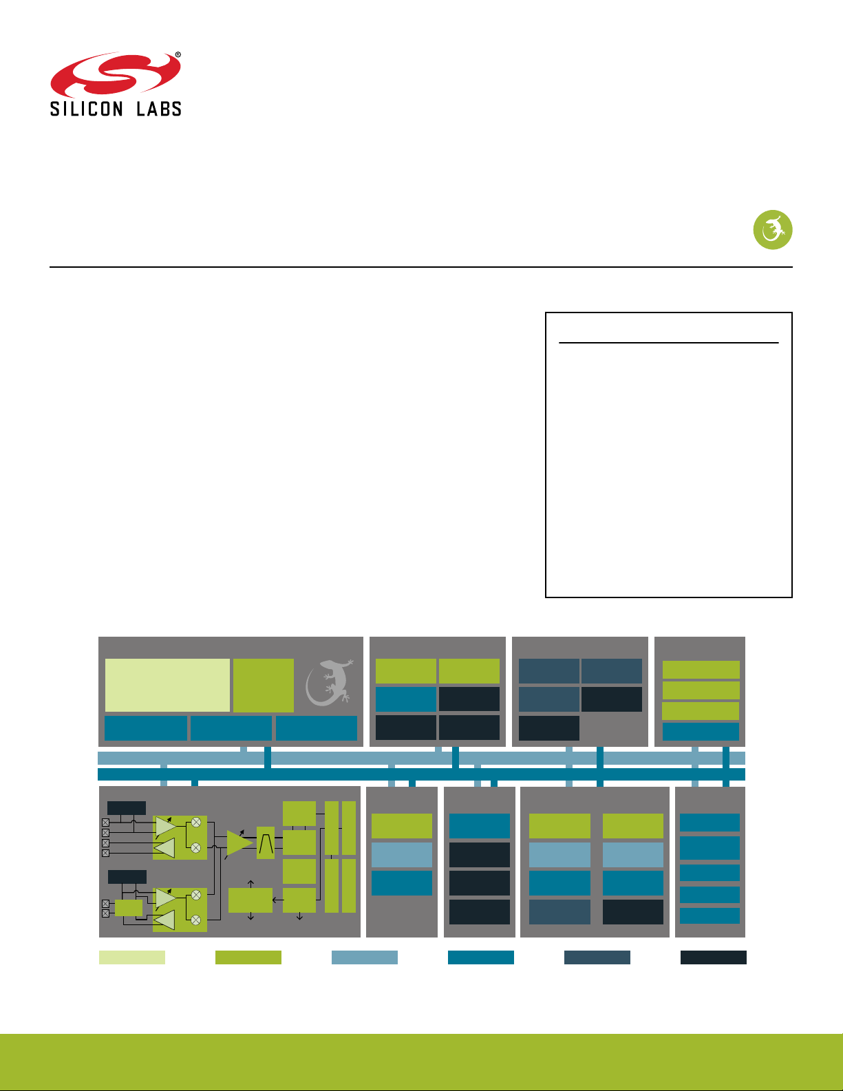
Core / Memory
TM
ARM Cortex
with DSP extensions, FPU and MPU
Debug Interface RAM Memory LDMA Controller
M4 processor
Flash Program
Memory
Clock Management
H-F Crystal
Oscillator
Auxiliary H-F RC
Oscillator
L-F Crystal
Oscillator
H-F
RC Oscillator
L-F
RC Oscillator
Ultra L-F RC
Oscillator
KEY FEATURES
• 32-bit ARM® Cortex-M4 core with 40 MHz
maximum operating frequency
• Scalable Memory and Radio configuration
options available in several footprint
compatible QFN packages
• 12-channel Peripheral Reflex System
enabling autonomous interaction of MCU
peripherals
• Autonomous Hardware Crypto Accelerator
and True Random Number Generator
• Integrated balun for 2.4 GHz and
integrated PA with up to 19 dBm transmit
power for 2.4 GHz and 20 dBm transmit
power for Sub-GHz radios
• Integrated DC-DC with RF noise mitigation
Energy Management
Voltage
Regulator
DC-DC
Converter
Brown-Out
Detector
Voltage Monitor
Power-On Reset
Other
CRYPTO
CRC
True Random
Number Generator
SMU
32-bit bus
Peripheral Reflex System
RFSENSE
RFSENSE
Lowest power mode with peripheral operational:
BALUN
Sub GHz
LNA
RF Frontend
PA
2.4 GHz
LNA
RF Frontend
PA
I
Q
I
Q
PGA
To Sub GHz
receive I/Q
mixers and PA
Frequency
Synthesizer
To 2.4 GHz receive
I/Q mixers and PA
Radio Transceiver
DEMOD
IFADC
AGC
MOD
To Sub GHz
and 2.4 GHz PA
FRC
CRC
BUFC
RAC
Serial
Interfaces
USART
Low Energy
TM
UART
2
I
C
I/O Ports Analog I/F
External
Interrupts
General
Purpose I/O
Pin Reset
Pin Wakeup
EM3—StopEM2—Deep SleepEM1—Sleep EM4—Hibernate EM4—ShutoffEM0—Active
Timers and Triggers
Timer/Counter
Low Energy
Timer
Pulse Counter Watchdog Timer
Real Time
Counter and
Calendar
Protocol Timer
Low Energy
Sensor Interface
Cryotimer
ADC
Analog
Comparator
IDAC
VDAC
Op-Amp
silabs.com | Building a more connected world. Rev. 1.1
Page 2

Table of Contents
1. About This Document ........................... 26
1.1 Introduction...............................26
1.2 Conventions ..............................26
1.3 Related Documentation ..........................27
2. System Overview ............................. 28
2.1 Introduction...............................28
2.2 Block Diagrams .............................29
2.3 MCU Features Overview ..........................30
2.4 Oscillators and Clocks ...........................32
2.5 RF Frequency Synthesizer .........................32
2.6 Modulation Modes ............................32
2.7 Transmit Mode .............................33
2.8 Receive Mode ..............................33
2.9 Data Buffering ..............................33
2.10 Unbuffered Data Transfer .........................33
2.11 Frame Format Support ..........................33
2.12 Hardware CRC Support ..........................34
2.13 Convolutional Encoding / Decoding ......................34
2.14 Binary Block Encoding / Decoding ......................34
2.15 Data Encryption and Authentication ......................35
2.16 Timers ................................36
2.17 RF Test Modes .............................36
3. System Processor ............................ 37
3.1 Introduction...............................37
3.2 Features................................38
3.3 Functional Description ...........................38
3.3.1 Interrupt Operation ..........................39
3.3.2 Interrupt Request Lines (IRQ) ......................40
4. Memory and Bus System .......................... 41
4.1 Introduction...............................42
4.2 Functional Description ...........................43
4.2.1 Peripheral Non-Word Access Behavior ...................45
4.2.2 Bit-banding .............................45
4.2.3 Peripheral Bit Set and Clear .......................46
4.2.4 Peripherals .............................47
4.2.5 Bus Matrix .............................48
4.3 Access to Low Energy Peripherals (Asynchronous Registers) ..............51
silabs.com
| Building a more connected world. Rev. 1.1 | 2
Page 3

4.3.1 Writing ..............................52
4.3.2 Reading ..............................54
4.3.3 FREEZE Register ..........................54
4.4 Flash .................................54
4.5 SRAM ................................55
4.6 DI Page Entry Map ............................56
4.7 DI Page Entry Description ..........................58
4.7.1 CAL - CRC of DI-page and calibration temperature ...............58
4.7.2 EXTINFO - External Component description .................59
4.7.3 EUI48L - EUI48 OUI and Unique identifier ..................60
4.7.4 EUI48H - OUI ...........................60
4.7.5 CUSTOMINFO - Custom information ...................60
4.7.6 MEMINFO - Flash page size and misc. chip information .............61
4.7.7 UNIQUEL - Low 32 bits of device unique number ...............62
4.7.8 UNIQUEH - High 32 bits of device unique number ...............62
4.7.9 MSIZE - Flash and SRAM Memory size in kB .................62
4.7.10 PART - Part description ........................63
4.7.11 DEVINFOREV - Device information page revision ...............65
4.7.12 EMUTEMP - EMU Temperature Calibration Information .............65
4.7.13 ADC0CAL0 - ADC0 calibration register 0 ..................66
4.7.14 ADC0CAL1 - ADC0 calibration register 1 ..................67
4.7.15 ADC0CAL2 - ADC0 calibration register 2 ..................68
4.7.16 ADC0CAL3 - ADC0 calibration register 3 ..................68
4.7.17 HFRCOCAL0 - HFRCO Calibration Register (4 MHz) ..............69
4.7.18 HFRCOCAL3 - HFRCO Calibration Register (7 MHz) ..............70
4.7.19 HFRCOCAL6 - HFRCO Calibration Register (13 MHz) .............71
4.7.20 HFRCOCAL7 - HFRCO Calibration Register (16 MHz) .............72
4.7.21 HFRCOCAL8 - HFRCO Calibration Register (19 MHz) .............73
4.7.22 HFRCOCAL10 - HFRCO Calibration Register (26 MHz) .............74
4.7.23 HFRCOCAL11 - HFRCO Calibration Register (32 MHz) .............75
4.7.24 HFRCOCAL12 - HFRCO Calibration Register (38 MHz) .............76
4.7.25 AUXHFRCOCAL0 - AUXHFRCO Calibration Register (4 MHz) ..........77
4.7.26 AUXHFRCOCAL3 - AUXHFRCO Calibration Register (7 MHz) ..........78
4.7.27 AUXHFRCOCAL6 - AUXHFRCO Calibration Register (13 MHz) ..........79
4.7.28 AUXHFRCOCAL7 - AUXHFRCO Calibration Register (16 MHz) ..........80
4.7.29 AUXHFRCOCAL8 - AUXHFRCO Calibration Register (19 MHz) ..........81
4.7.30 AUXHFRCOCAL10 - AUXHFRCO Calibration Register (26 MHz) .........82
4.7.31 AUXHFRCOCAL11 - AUXHFRCO Calibration Register (32 MHz) ..........83
4.7.32 AUXHFRCOCAL12 - AUXHFRCO Calibration Register (38 MHz) .........84
4.7.33 VMONCAL0 - VMON Calibration Register 0 .................85
4.7.34 VMONCAL1 - VMON Calibration Register 1 .................86
4.7.35 VMONCAL2 - VMON Calibration Register 2 .................87
4.7.36 IDAC0CAL0 - IDAC0 Calibration Register 0 .................88
4.7.37 IDAC0CAL1 - IDAC0 Calibration Register 1 .................89
4.7.38 DCDCLNVCTRL0 - DCDC Low-noise VREF Trim Register 0 ...........89
4.7.39 DCDCLPVCTRL0 - DCDC Low-power VREF Trim Register 0 ...........90
4.7.40 DCDCLPVCTRL1 - DCDC Low-power VREF Trim Register 1 ...........91
silabs.com
| Building a more connected world. Rev. 1.1 | 3
Page 4

4.7.41 DCDCLPVCTRL2 - DCDC Low-power VREF Trim Register 2 ...........92
4.7.42 DCDCLPVCTRL3 - DCDC Low-power VREF Trim Register 3 ...........93
4.7.43 DCDCLPCMPHYSSEL0 - DCDC LPCMPHYSSEL Trim Register 0 .........93
4.7.44 DCDCLPCMPHYSSEL1 - DCDC LPCMPHYSSEL Trim Register 1 .........94
4.7.45 VDAC0MAINCAL - VDAC0 Cals for Main Path ................95
4.7.46 VDAC0ALTCAL - VDAC0 Cals for Alternate Path ...............96
4.7.47 VDAC0CH1CAL - VDAC0 CH1 Error Cal ..................97
4.7.48 OPA0CAL0 - OPA0 Calibration Register for DRIVESTRENGTH 0, INCBW=1 .....98
4.7.49 OPA0CAL1 - OPA0 Calibration Register for DRIVESTRENGTH 1, INCBW=1 .....99
4.7.50 OPA0CAL2 - OPA0 Calibration Register for DRIVESTRENGTH 2, INCBW=1 ....100
4.7.51 OPA0CAL3 - OPA0 Calibration Register for DRIVESTRENGTH 3, INCBW=1 ....101
4.7.52 OPA1CAL0 - OPA1 Calibration Register for DRIVESTRENGTH 0, INCBW=1 ....102
4.7.53 OPA1CAL1 - OPA1 Calibration Register for DRIVESTRENGTH 1, INCBW=1 ....103
4.7.54 OPA1CAL2 - OPA1 Calibration Register for DRIVESTRENGTH 2, INCBW=1 ....104
4.7.55 OPA1CAL3 - OPA1 Calibration Register for DRIVESTRENGTH 3, INCBW=1 ....105
4.7.56 OPA0CAL4 - OPA0 Calibration Register for DRIVESTRENGTH 0, INCBW=0 ....106
4.7.57 OPA0CAL5 - OPA0 Calibration Register for DRIVESTRENGTH 1, INCBW=0 ....107
4.7.58 OPA0CAL6 - OPA0 Calibration Register for DRIVESTRENGTH 2, INCBW=0 ....108
4.7.59 OPA0CAL7 - OPA0 Calibration Register for DRIVESTRENGTH 3, INCBW=0 ....109
4.7.60 OPA1CAL4 - OPA1 Calibration Register for DRIVESTRENGTH 0, INCBW=0 ....110
4.7.61 OPA1CAL5 - OPA1 Calibration Register for DRIVESTRENGTH 1, INCBW=0 ....111
4.7.62 OPA1CAL6 - OPA1 Calibration Register for DRIVESTRENGTH 2, INCBW=0 ....112
4.7.63 OPA1CAL7 - OPA1 Calibration Register for DRIVESTRENGTH 3, INCBW=0 ....113
5. Radio Transceiver ............................114
5.1 Introduction..............................115
6. DBG - Debug Interface ...........................116
6.1 Introduction..............................116
6.2 Features...............................116
6.3 Functional Description ..........................116
6.3.1 Debug Pins............................117
6.3.2 Debug and EM2 Deep Sleep/EM3 Stop ..................117
6.3.3 Authentication Access Point ......................117
6.3.4 Debug Lock ...........................118
6.3.5 AAP Lock ............................118
6.3.6 Debugger Reads of Actionable Registers .................119
6.3.7 Debug Recovery ..........................119
6.4 Register Map .............................119
6.5 Register Description ...........................120
6.5.1 AAP_CMD - Command Register ....................120
6.5.2 AAP_CMDKEY - Command Key Register .................120
6.5.3 AAP_STATUS - Status Register ....................121
6.5.4 AAP_CTRL - Control Register .....................121
6.5.5 AAP_CRCCMD - CRC Command Register ................122
6.5.6 AAP_CRCSTATUS - CRC Status Register .................122
6.5.7 AAP_CRCADDR - CRC Address Register .................123
6.5.8 AAP_CRCRESULT - CRC Result Register .................123
silabs.com
| Building a more connected world. Rev. 1.1 | 4
Page 5

6.5.9 AAP_IDR - AAP Identification Register ..................124
7. MSC - Memory System Controller ......................125
7.1 Introduction..............................125
7.2 Features...............................126
7.3 Functional Description ..........................127
7.3.1 User Data (UD) Page Description ....................127
7.3.2 Lock Bits (LB) Page Description.....................128
7.3.3 Device Information (DI) Page .....................128
7.3.4 Bootloader ............................129
7.3.5 Device Revision ..........................129
7.3.6 Post-reset Behavior .........................129
7.3.7 Flash Startup ...........................130
7.3.8 Wait-states ............................130
7.3.9 Suppressed Conditional Branch Target Prefetch (SCBTP) ............131
7.3.10 Cortex-M4 If-Then Block Folding ....................131
7.3.11 Instruction Cache .........................132
7.3.12 Low Voltage Flash Read .......................133
7.3.13 Erase and Write Operations......................133
7.4 Register Map .............................134
7.5 Register Description ...........................135
7.5.1 MSC_CTRL - Memory System Control Register ...............135
7.5.2 MSC_READCTRL - Read Control Register ................136
7.5.3 MSC_WRITECTRL - Write Control Register ................137
7.5.4 MSC_WRITECMD - Write Command Register ...............138
7.5.5 MSC_ADDRB - Page Erase/Write Address Buffer ..............139
7.5.6 MSC_WDATA - Write Data Register ...................139
7.5.7 MSC_STATUS - Status Register ....................140
7.5.8 MSC_IF - Interrupt Flag Register ....................141
7.5.9 MSC_IFS - Interrupt Flag Set Register ..................142
7.5.10 MSC_IFC - Interrupt Flag Clear Register .................143
7.5.11 MSC_IEN - Interrupt Enable Register ..................144
7.5.12 MSC_LOCK - Configuration Lock Register ................145
7.5.13 MSC_CACHECMD - Flash Cache Command Register ............146
7.5.14 MSC_CACHEHITS - Cache Hits Performance Counter ............146
7.5.15 MSC_CACHEMISSES - Cache Misses Performance Counter ..........147
7.5.16 MSC_MASSLOCK - Mass Erase Lock Register ..............148
7.5.17 MSC_STARTUP - Startup Control ...................149
7.5.18 MSC_CMD - Command Register ...................150
7.5.19 MSC_BOOTLOADERCTRL - Bootloader Read and Write Enable, Write Once Register . 150
7.5.20 MSC_AAPUNLOCKCMD - Software Unlock AAP Command Register .......151
7.5.21 MSC_CACHECONFIG0 - Cache Configuration Register 0 ...........152
8. LDMA - Linked DMA Controller........................153
8.1 Introduction..............................153
8.1.1 Features ............................154
8.2 Block Diagram.............................155
silabs.com
| Building a more connected world. Rev. 1.1 | 5
Page 6

8.3 Functional Description ..........................156
8.3.1 Channel Descriptor .........................156
8.3.2 Channel Configuration ........................161
8.3.3 Channel Select Configuration .....................161
8.3.4 Starting a Transfer .........................161
8.3.5 Managing Transfer Errors .......................162
8.3.6 Arbitration ............................162
8.3.7 Channel Descriptor Data Structure ....................165
8.3.8 Interaction With the EMU .......................167
8.3.9 Interrupts ............................168
8.3.10 Debugging ...........................168
8.4 Examples ..............................168
8.4.1 Single Direct Register DMA Transfer ...................168
8.4.2 Descriptor Linked List ........................169
8.4.3 Single Descriptor Looped Transfer ....................171
8.4.4 Descriptor List With Looping ......................172
8.4.5 Simple Inter-Channel Synchronization...................173
8.4.6 2D Copy.............................175
8.4.7 Ping-Pong ............................177
8.4.8 Scatter-Gather ..........................178
8.5 Register Map .............................179
8.6 Register Description ...........................180
8.6.1 LDMA_CTRL - DMA Control Register ..................180
8.6.2 LDMA_STATUS - DMA Status Register ..................181
8.6.3 LDMA_SYNC - DMA Synchronization Trigger Register (Single-Cycle RMW) .....182
8.6.4 LDMA_CHEN - DMA Channel Enable Register (Single-Cycle RMW) ........182
8.6.5 LDMA_CHBUSY - DMA Channel Busy Register ...............183
8.6.6 LDMA_CHDONE - DMA Channel Linking Done Register (Single-Cycle RMW) .....183
8.6.7 LDMA_DBGHALT - DMA Channel Debug Halt Register ............184
8.6.8 LDMA_SWREQ - DMA Channel Software Transfer Request Register ........184
8.6.9 LDMA_REQDIS - DMA Channel Request Disable Register ...........185
8.6.10 LDMA_REQPEND - DMA Channel Requests Pending Register .........185
8.6.11 LDMA_LINKLOAD - DMA Channel Link Load Register ............186
8.6.12 LDMA_REQCLEAR - DMA Channel Request Clear Register ..........186
8.6.13 LDMA_IF - Interrupt Flag Register ...................187
8.6.14 LDMA_IFS - Interrupt Flag Set Register .................187
8.6.15 LDMA_IFC - Interrupt Flag Clear Register ................188
8.6.16 LDMA_IEN - Interrupt Enable Register .................188
8.6.17 LDMA_CHx_REQSEL - Channel Peripheral Request Select Register .......189
8.6.18 LDMA_CHx_CFG - Channel Configuration Register .............192
8.6.19 LDMA_CHx_LOOP - Channel Loop Counter Register ............193
8.6.20 LDMA_CHx_CTRL - Channel Descriptor Control Word Register .........194
8.6.21 LDMA_CHx_SRC - Channel Descriptor Source Data Address Register ......197
8.6.22 LDMA_CHx_DST - Channel Descriptor Destination Data Address Register .....197
8.6.23 LDMA_CHx_LINK - Channel Descriptor Link Structure Address Register ......198
9. RMU - Reset Management Unit ........................199
9.1 Introduction..............................199
silabs.com
| Building a more connected world. Rev. 1.1 | 6
Page 7

9.2 Features...............................199
9.3 Functional Description ..........................200
9.3.1 Reset Levels ...........................201
9.3.2 RMU_RSTCAUSE Register ......................202
9.3.3 Power-On Reset (POR) .......................203
9.3.4 Brown-Out Detector (BOD) ......................203
9.3.5 RESETn Pin Reset .........................204
9.3.6 Watchdog Reset ..........................204
9.3.7 Lockup Reset ...........................204
9.3.8 System Reset Request ........................204
9.3.9 Reset State ...........................204
9.3.10 Register Reset Signals .......................204
9.4 Register Map .............................206
9.5 Register Description ...........................207
9.5.1 RMU_CTRL - Control Register .....................207
9.5.2 RMU_RSTCAUSE - Reset Cause Register ................209
9.5.3 RMU_CMD - Command Register ....................210
9.5.4 RMU_RST - Reset Control Register ...................210
9.5.5 RMU_LOCK - Configuration Lock Register .................211
10. EMU - Energy Management Unit .......................212
10.1 Introduction .............................212
10.2 Features ..............................213
10.3 Functional Description .........................214
10.3.1 Energy Modes ..........................215
10.3.2 Entering Low Energy Modes .....................219
10.3.3 Exiting a Low Energy Mode .....................221
10.3.4 Power Configurations ........................222
10.3.5 DC-to-DC Interface ........................226
10.3.6 Analog Peripheral Power Selection ...................228
10.3.7 Digital LDO Power Selection .....................229
10.3.8 IOVDD Connection.........................229
10.3.9 Voltage Scaling ..........................230
10.3.10 EM23 Peripheral Retention Disable...................232
10.3.11 Brown Out Detector (BOD)......................232
10.3.12 Voltage Monitor (VMON) ......................233
10.3.13 Powering Off SRAM Blocks .....................234
10.3.14 Temperature Sensor ........................234
10.3.15 Registers latched in EM4 ......................235
10.3.16 Register Resets .........................235
10.4 Register Map.............................236
10.5 Register Description ..........................238
10.5.1 EMU_CTRL - Control Register ....................238
10.5.2 EMU_STATUS - Status Register ....................240
10.5.3 EMU_LOCK - Configuration Lock Register ................242
10.5.4 EMU_RAM0CTRL - Memory Control Register ...............242
silabs.com
| Building a more connected world. Rev. 1.1 | 7
Page 8

10.5.5 EMU_CMD - Command Register ...................243
10.5.6 EMU_EM4CTRL - EM4 Control Register .................244
10.5.7 EMU_TEMPLIMITS - Temperature Limits for Interrupt Generation ........245
10.5.8 EMU_TEMP - Value of Last Temperature Measurement ............245
10.5.9 EMU_IF - Interrupt Flag Register ...................246
10.5.10 EMU_IFS - Interrupt Flag Set Register .................248
10.5.11 EMU_IFC - Interrupt Flag Clear Register ................250
10.5.12 EMU_IEN - Interrupt Enable Register .................252
10.5.13 EMU_PWRLOCK - Regulator and Supply Lock Register ...........254
10.5.14 EMU_PWRCTRL - Power Control Register ................255
10.5.15 EMU_DCDCCTRL - DCDC Control ..................256
10.5.16 EMU_DCDCMISCCTRL - DCDC Miscellaneous Control Register ........257
10.5.17 EMU_DCDCZDETCTRL - DCDC Power Train NFET Zero Current Detector Control Register
................................259
10.5.18 EMU_DCDCCLIMCTRL - DCDC Power Train PFET Current Limiter Control Register . 260
10.5.19 EMU_DCDCLNCOMPCTRL - DCDC Low Noise Compensator Control Register ...261
10.5.20 EMU_DCDCLNVCTRL - DCDC Low Noise Voltage Register ..........262
10.5.21 EMU_DCDCLPVCTRL - DCDC Low Power Voltage Register .........263
10.5.22 EMU_DCDCLPCTRL - DCDC Low Power Control Register ..........264
10.5.23 EMU_DCDCLNFREQCTRL - DCDC Low Noise Controller Frequency Control ....265
10.5.24 EMU_DCDCSYNC - DCDC Read Status Register .............265
10.5.25 EMU_VMONAVDDCTRL - VMON AVDD Channel Control ..........266
10.5.26 EMU_VMONALTAVDDCTRL - Alternate VMON AVDD Channel Control ......267
10.5.27 EMU_VMONDVDDCTRL - VMON DVDD Channel Control ..........268
10.5.28 EMU_VMONIO0CTRL - VMON IOVDD0 Channel Control ...........269
10.5.29 EMU_RAM1CTRL - Memory Control Register ...............270
10.5.30 EMU_RAM2CTRL - Memory Control Register ...............271
10.5.31 EMU_DCDCLPEM01CFG - Configuration Bits for Low Power Mode to Be Applied During
EM01, This Field is Only Relevant If LP Mode is Used in EM01 ...........272
10.5.32 EMU_EM23PERNORETAINCMD - Clears Corresponding Bits in EM23PERNORETAINSTA-
TUS Unlocking Access to Peripheral ....................273
10.5.33 EMU_EM23PERNORETAINSTATUS - Status Indicating If Peripherals Were Powered Down
in EM23, Subsequently Locking Access to It .................275
10.5.34 EMU_EM23PERNORETAINCTRL - When Set Corresponding Peripherals May Get Powered
Down in EM23 ...........................277
11. CMU - Clock Management Unit .......................279
11.1 Introduction .............................279
11.2 Features ..............................279
11.3 Functional Description..........................280
11.3.1 System Clocks ..........................281
11.3.2 Oscillators............................284
11.3.3 Configuration for Operating Frequencies .................302
11.3.4 Energy Modes ..........................303
11.3.5 Clock Output on a Pin ........................304
11.3.6 Clock Input From a Pin .......................304
11.3.7 Clock Output on PRS ........................304
11.3.8 Error Handling ..........................304
silabs.com
| Building a more connected world. Rev. 1.1 | 8
Page 9

11.3.9 Interrupts ............................304
11.3.10 Wake-up ............................305
11.3.11 Protection ...........................305
11.4 Register Map .............................306
11.5 Register Description ..........................308
11.5.1 CMU_CTRL - CMU Control Register ..................308
11.5.2 CMU_HFRCOCTRL - HFRCO Control Register ..............310
11.5.3 CMU_AUXHFRCOCTRL - AUXHFRCO Control Register ...........312
11.5.4 CMU_LFRCOCTRL - LFRCO Control Register ...............313
11.5.5 CMU_HFXOCTRL - HFXO Control Register ................315
11.5.6 CMU_HFXOSTARTUPCTRL - HFXO Startup Control .............317
11.5.7 CMU_HFXOSTEADYSTATECTRL - HFXO Steady State Control .........318
11.5.8 CMU_HFXOTIMEOUTCTRL - HFXO Timeout Control ............319
11.5.9 CMU_LFXOCTRL - LFXO Control Register ................322
11.5.10 CMU_CALCTRL - Calibration Control Register ..............324
11.5.11 CMU_CALCNT - Calibration Counter Register ...............326
11.5.12 CMU_OSCENCMD - Oscillator Enable/Disable Command Register .......327
11.5.13 CMU_CMD - Command Register ...................328
11.5.14 CMU_DBGCLKSEL - Debug Trace Clock Select ..............329
11.5.15 CMU_HFCLKSEL - High Frequency Clock Select Command Register ......329
11.5.16 CMU_LFACLKSEL - Low Frequency A Clock Select Register .........330
11.5.17 CMU_LFBCLKSEL - Low Frequency B Clock Select Register .........330
11.5.18 CMU_LFECLKSEL - Low Frequency E Clock Select Register .........331
11.5.19 CMU_STATUS - Status Register ...................332
11.5.20 CMU_HFCLKSTATUS - HFCLK Status Register ..............334
11.5.21 CMU_HFXOTRIMSTATUS - HFXO Trim Status ..............335
11.5.22 CMU_IF - Interrupt Flag Register ...................336
11.5.23 CMU_IFS - Interrupt Flag Set Register .................338
11.5.24 CMU_IFC - Interrupt Flag Clear Register ................340
11.5.25 CMU_IEN - Interrupt Enable Register .................342
11.5.26 CMU_HFBUSCLKEN0 - High Frequency Bus Clock Enable Register 0 ......344
11.5.27 CMU_HFPERCLKEN0 - High Frequency Peripheral Clock Enable Register 0 ....345
11.5.28 CMU_HFRADIOALTCLKEN0 - High Frequency Alternate Radio Peripheral Clock Enable
Register 0 .............................346
11.5.29 CMU_LFACLKEN0 - Low Frequency a Clock Enable Register 0 (Async Reg) ....346
11.5.30 CMU_LFBCLKEN0 - Low Frequency B Clock Enable Register 0 (Async Reg) ....347
11.5.31 CMU_LFECLKEN0 - Low Frequency E Clock Enable Register 0 (Async Reg) ....347
11.5.32 CMU_HFPRESC - High Frequency Clock Prescaler Register .........348
11.5.33 CMU_HFCOREPRESC - High Frequency Core Clock Prescaler Register .....349
11.5.34 CMU_HFPERPRESC - High Frequency Peripheral Clock Prescaler Register ....349
11.5.35 CMU_HFRADIOPRESC - High Frequency Radio Peripheral Clock Prescaler Register . 350
11.5.36 CMU_HFEXPPRESC - High Frequency Export Clock Prescaler Register .....350
11.5.37 CMU_LFAPRESC0 - Low Frequency a Prescaler Register 0 (Async Reg) .....351
11.5.38 CMU_LFBPRESC0 - Low Frequency B Prescaler Register 0 (Async Reg) .....352
11.5.39 CMU_LFEPRESC0 - Low Frequency E Prescaler Register 0 (Async Reg) .....353
11.5.40 CMU_HFRADIOALTPRESC - High Frequency Alternate Radio Peripheral Clock Prescaler
Register .............................353
11.5.41 CMU_SYNCBUSY - Synchronization Busy Register .............354
silabs.com
| Building a more connected world. Rev. 1.1 | 9
Page 10

11.5.42 CMU_FREEZE - Freeze Register ...................357
11.5.43 CMU_PCNTCTRL - PCNT Control Register ...............358
11.5.44 CMU_ADCCTRL - ADC Control Register ................359
11.5.45 CMU_ROUTEPEN - I/O Routing Pin Enable Register ............360
11.5.46 CMU_ROUTELOC0 - I/O Routing Location Register ............361
11.5.47 CMU_ROUTELOC1 - I/O Routing Location Register ............362
11.5.48 CMU_LOCK - Configuration Lock Register ................363
12. SMU - Security Management Unit ......................364
12.1 Introduction .............................364
12.2 Features ..............................364
12.3 Functional Description .........................365
12.3.1 PPU - Peripheral Protection Unit ....................365
12.3.2 Programming Model ........................366
12.4 Register Map.............................367
12.5 Register Description ..........................368
12.5.1 SMU_IF - Interrupt Flag Register ...................368
12.5.2 SMU_IFS - Interrupt Flag Set Register ..................368
12.5.3 SMU_IFC - Interrupt Flag Clear Register .................369
12.5.4 SMU_IEN - Interrupt Enable Register ..................369
12.5.5 SMU_PPUCTRL - PPU Control Register .................370
12.5.6 SMU_PPUPATD0 - PPU Privilege Access Type Descriptor 0 ..........371
12.5.7 SMU_PPUPATD1 - PPU Privilege Access Type Descriptor 1 ..........373
12.5.8 SMU_PPUFS - PPU Fault Status ...................374
13. RTCC - Real Time Counter and Calendar ...................376
13.1 Introduction .............................376
13.2 Features ..............................376
13.3 Functional Description .........................377
13.3.1 Counter ............................378
13.3.2 Capture/Compare Channels .....................382
13.3.3 Interrupts and PRS Output ......................384
13.3.4 Energy Mode Availability .......................385
13.3.5 Register Lock ..........................385
13.3.6 Oscillator Failure Detection ......................385
13.3.7 Retention Registers ........................385
13.3.8 Debug Session ..........................385
13.4 Register Map.............................386
13.5 Register Description ..........................387
13.5.1 RTCC_CTRL - Control Register (Async Reg) ...............387
13.5.2 RTCC_PRECNT - Pre-Counter Value Register (Async Reg) ..........389
13.5.3 RTCC_CNT - Counter Value Register (Async Reg) .............389
13.5.4 RTCC_COMBCNT - Combined Pre-Counter and Counter Value Register ......390
13.5.5 RTCC_TIME - Time of Day Register (Async Reg) ..............391
13.5.6 RTCC_DATE - Date Register (Async Reg) ................392
13.5.7 RTCC_IF - RTCC Interrupt Flags ...................393
silabs.com
| Building a more connected world. Rev. 1.1 | 10
Page 11

13.5.8 RTCC_IFS - Interrupt Flag Set Register .................394
13.5.9 RTCC_IFC - Interrupt Flag Clear Register ................395
13.5.10 RTCC_IEN - Interrupt Enable Register .................396
13.5.11 RTCC_STATUS - Status Register ...................397
13.5.12 RTCC_CMD - Command Register ...................397
13.5.13 RTCC_SYNCBUSY - Synchronization Busy Register ............397
13.5.14 RTCC_POWERDOWN - Retention RAM Power-down Register (Async Reg) ....398
13.5.15 RTCC_LOCK - Configuration Lock Register (Async Reg) ...........398
13.5.16 RTCC_EM4WUEN - Wake Up Enable .................399
13.5.17 RTCC_CCx_CTRL - CC Channel Control Register (Async Reg) ........400
13.5.18 RTCC_CCx_CCV - Capture/Compare Value Register (Async Reg) ........402
13.5.19 RTCC_CCx_TIME - Capture/Compare Time Register (Async Reg) ........403
13.5.20 RTCC_CCx_DATE - Capture/Compare Date Register (Async Reg) .......404
13.5.21 RTCC_RETx_REG - Retention Register .................404
14. WDOG - Watchdog Timer .........................405
14.1 Introduction .............................405
14.2 Features ..............................405
14.3 Functional Description .........................405
14.3.1 Clock Source ..........................406
14.3.2 Debug Functionality ........................406
14.3.3 Energy Mode Handling .......................406
14.3.4 Register Access..........................406
14.3.5 Warning Interrupt .........................406
14.3.6 Window Interrupt .........................407
14.3.7 PRS as Watchdog Clear .......................408
14.3.8 PRS Rising Edge Monitoring .....................408
14.4 Register Map.............................409
14.5 Register Description ..........................410
14.5.1 WDOG_CTRL - Control Register (Async Reg) ...............410
14.5.2 WDOG_CMD - Command Register (Async Reg) ..............413
14.5.3 WDOG_SYNCBUSY - Synchronization Busy Register ............414
14.5.4 WDOGn_PCHx_PRSCTRL - PRS Control Register (Async Reg) .........415
14.5.5 WDOG_IF - Watchdog Interrupt Flags ..................416
14.5.6 WDOG_IFS - Interrupt Flag Set Register .................417
14.5.7 WDOG_IFC - Interrupt Flag Clear Register ................418
14.5.8 WDOG_IEN - Interrupt Enable Register .................419
15. PRS - Peripheral Reflex System .......................420
15.1 Introduction .............................420
15.2 Features ..............................420
15.3 Functional Description .........................421
15.3.1 Channel Functions .........................421
15.3.2 Producers............................422
15.3.3 Consumers ...........................423
15.3.4 Event on PRS ..........................424
15.3.5 DMA Request on PRS .......................424
silabs.com
| Building a more connected world. Rev. 1.1 | 11
Page 12

15.3.6 Example ............................425
15.4 Register Map.............................425
15.5 Register Description ..........................426
15.5.1 PRS_SWPULSE - Software Pulse Register ................426
15.5.2 PRS_SWLEVEL - Software Level Register ................427
15.5.3 PRS_ROUTEPEN - I/O Routing Pin Enable Register .............428
15.5.4 PRS_ROUTELOC0 - I/O Routing Location Register .............429
15.5.5 PRS_ROUTELOC1 - I/O Routing Location Register .............432
15.5.6 PRS_ROUTELOC2 - I/O Routing Location Register .............434
15.5.7 PRS_CTRL - Control Register ....................436
15.5.8 PRS_DMAREQ0 - DMA Request 0 Register ................437
15.5.9 PRS_DMAREQ1 - DMA Request 1 Register ................438
15.5.10 PRS_PEEK - PRS Channel Values ..................439
15.5.11 PRS_CHx_CTRL - Channel Control Register ...............440
16. PCNT - Pulse Counter ..........................446
16.1 Introduction .............................446
16.2 Features ..............................446
16.3 Functional Description .........................447
16.3.1 Pulse Counter Modes ........................447
16.3.2 Hysteresis ...........................454
16.3.3 Auxiliary Counter .........................455
16.3.4 Triggered Compare and Clear .....................456
16.3.5 Register Access..........................457
16.3.6 Clock Sources ..........................457
16.3.7 Input Filter ...........................457
16.3.8 Edge Polarity ..........................458
16.3.9 PRS and PCNTn_S0IN,PCNTn_S1IN Inputs ................458
16.3.10 Interrupts ...........................458
16.3.11 Cascading Pulse Counters......................460
16.4 Register Map.............................461
16.5 Register Description ..........................462
16.5.1 PCNTn_CTRL - Control Register (Async Reg) ...............462
16.5.2 PCNTn_CMD - Command Register (Async Reg) ..............466
16.5.3 PCNTn_STATUS - Status Register ...................466
16.5.4 PCNTn_CNT - Counter Value Register .................467
16.5.5 PCNTn_TOP - Top Value Register ...................467
16.5.6 PCNTn_TOPB - Top Value Buffer Register (Async Reg) ............468
16.5.7 PCNTn_IF - Interrupt Flag Register ...................468
16.5.8 PCNTn_IFS - Interrupt Flag Set Register .................469
16.5.9 PCNTn_IFC - Interrupt Flag Clear Register ................470
16.5.10 PCNTn_IEN - Interrupt Enable Register .................471
16.5.11 PCNTn_ROUTELOC0 - I/O Routing Location Register ............472
16.5.12 PCNTn_FREEZE - Freeze Register ..................474
16.5.13 PCNTn_SYNCBUSY - Synchronization Busy Register ............475
16.5.14 PCNTn_AUXCNT - Auxiliary Counter Value Register ............475
16.5.15 PCNTn_INPUT - PCNT Input Register .................476
silabs.com
| Building a more connected world. Rev. 1.1 | 12
Page 13

16.5.16 PCNTn_OVSCFG - Oversampling Config Register (Async Reg) ........477
17. I2C - Inter-Integrated Circuit Interface.....................478
17.1 Introduction .............................478
17.2 Features ..............................478
17.3 Functional Description .........................479
17.3.1 I2C-Bus Overview .........................480
17.3.2 Enable and Reset .........................484
17.3.3 Safely Disabling and Changing Slave Configuration..............484
17.3.4 Clock Generation .........................484
17.3.5 Arbitration............................485
17.3.6 Buffers .............................485
17.3.7 Master Operation .........................487
17.3.8 Bus States ...........................495
17.3.9 Slave Operation .........................495
17.3.10 Transfer Automation ........................499
17.3.11 Using 10-bit Addresses .......................500
17.3.12 Error Handling ..........................500
17.3.13 DMA Support ..........................502
17.3.14 Interrupts ...........................502
17.3.15 Wake-up............................502
17.4 Register Map.............................503
17.5 Register Description ..........................504
17.5.1 I2Cn_CTRL - Control Register ....................504
17.5.2 I2Cn_CMD - Command Register ...................507
17.5.3 I2Cn_STATE - State Register .....................508
17.5.4 I2Cn_STATUS - Status Register ....................509
17.5.5 I2Cn_CLKDIV - Clock Division Register .................510
17.5.6 I2Cn_SADDR - Slave Address Register .................510
17.5.7 I2Cn_SADDRMASK - Slave Address Mask Register .............511
17.5.8 I2Cn_RXDATA - Receive Buffer Data Register (Actionable Reads) ........511
17.5.9 I2Cn_RXDOUBLE - Receive Buffer Double Data Register (Actionable Reads) ....512
17.5.10 I2Cn_RXDATAP - Receive Buffer Data Peek Register ............512
17.5.11 I2Cn_RXDOUBLEP - Receive Buffer Double Data Peek Register ........513
17.5.12 I2Cn_TXDATA - Transmit Buffer Data Register ..............513
17.5.13 I2Cn_TXDOUBLE - Transmit Buffer Double Data Register ..........514
17.5.14 I2Cn_IF - Interrupt Flag Register ...................515
17.5.15 I2Cn_IFS - Interrupt Flag Set Register .................517
17.5.16 I2Cn_IFC - Interrupt Flag Clear Register ................519
17.5.17 I2Cn_IEN - Interrupt Enable Register ..................521
17.5.18 I2Cn_ROUTEPEN - I/O Routing Pin Enable Register ............522
17.5.19 I2Cn_ROUTELOC0 - I/O Routing Location Register .............523
18. USART - Universal Synchronous Asynchronous Receiver/Transmitter ........526
18.1 Introduction .............................526
18.2 Features ..............................527
18.3 Functional Description .........................528
silabs.com
| Building a more connected world. Rev. 1.1 | 13
Page 14

18.3.1 Modes of Operation ........................529
18.3.2 Asynchronous Operation.......................529
18.3.3 Synchronous Operation .......................546
18.3.4 Hardware Flow Control .......................552
18.3.5 Debug Halt ...........................552
18.3.6 PRS-triggered Transmissions .....................552
18.3.7 PRS RX Input ..........................552
18.3.8 PRS CLK Input ..........................553
18.3.9 DMA Support ..........................553
18.3.10 Timer .............................554
18.3.11 Interrupts ...........................559
18.3.12 IrDA Modulator/ Demodulator.....................560
18.4 Register Map.............................561
18.5 Register Description ..........................562
18.5.1 USARTn_CTRL - Control Register ...................562
18.5.2 USARTn_FRAME - USART Frame Format Register .............567
18.5.3 USARTn_TRIGCTRL - USART Trigger Control Register ............569
18.5.4 USARTn_CMD - Command Register ..................571
18.5.5 USARTn_STATUS - USART Status Register ...............572
18.5.6 USARTn_CLKDIV - Clock Control Register ................573
18.5.7 USARTn_RXDATAX - RX Buffer Data Extended Register (Actionable Reads) ....574
18.5.8 USARTn_RXDATA - RX Buffer Data Register (Actionable Reads) ........574
18.5.9 USARTn_RXDOUBLEX - RX Buffer Double Data Extended Register (Actionable Reads) 575
18.5.10 USARTn_RXDOUBLE - RX FIFO Double Data Register (Actionable Reads) ....576
18.5.11 USARTn_RXDATAXP - RX Buffer Data Extended Peek Register ........576
18.5.12 USARTn_RXDOUBLEXP - RX Buffer Double Data Extended Peek Register ....577
18.5.13 USARTn_TXDATAX - TX Buffer Data Extended Register ...........578
18.5.14 USARTn_TXDATA - TX Buffer Data Register ...............579
18.5.15 USARTn_TXDOUBLEX - TX Buffer Double Data Extended Register .......580
18.5.16 USARTn_TXDOUBLE - TX Buffer Double Data Register ...........581
18.5.17 USARTn_IF - Interrupt Flag Register ..................582
18.5.18 USARTn_IFS - Interrupt Flag Set Register ................584
18.5.19 USARTn_IFC - Interrupt Flag Clear Register ...............586
18.5.20 USARTn_IEN - Interrupt Enable Register ................588
18.5.21 USARTn_IRCTRL - IrDA Control Register ................590
18.5.22 USARTn_INPUT - USART Input Register ................592
18.5.23 USARTn_I2SCTRL - I2S Control Register ................594
18.5.24 USARTn_TIMING - Timing Register ..................596
18.5.25 USARTn_CTRLX - Control Register Extended ..............598
18.5.26 USARTn_TIMECMP0 - Used to Generate Interrupts and Various Delays ......599
18.5.27 USARTn_TIMECMP1 - Used to Generate Interrupts and Various Delays ......601
18.5.28 USARTn_TIMECMP2 - Used to Generate Interrupts and Various Delays ......603
18.5.29 USARTn_ROUTEPEN - I/O Routing Pin Enable Register ...........605
18.5.30 USARTn_ROUTELOC0 - I/O Routing Location Register ...........607
18.5.31 USARTn_ROUTELOC1 - I/O Routing Location Register ...........612
19. LEUART - Low Energy Universal Asynchronous Receiver/Transmitter ........615
19.1 Introduction .............................615
silabs.com
| Building a more connected world. Rev. 1.1 | 14
Page 15

19.2 Features ..............................616
19.3 Functional Description .........................617
19.3.1 Frame Format ..........................618
19.3.2 Clock Source ..........................618
19.3.3 Clock Generation .........................619
19.3.4 Data Transmission .........................619
19.3.5 Data Reception ..........................621
19.3.6 Loopback ............................624
19.3.7 Half Duplex Communication .....................624
19.3.8 Transmission Delay ........................625
19.3.9 PRS RX Input ..........................626
19.3.10 DMA Support ..........................626
19.3.11 Pulse Generator/ Pulse Extender ...................627
19.3.12 Register Access .........................627
19.4 Register Map.............................628
19.5 Register Description ..........................629
19.5.1 LEUARTn_CTRL - Control Register (Async Reg) ..............629
19.5.2 LEUARTn_CMD - Command Register (Async Reg) .............632
19.5.3 LEUARTn_STATUS - Status Register ..................633
19.5.4 LEUARTn_CLKDIV - Clock Control Register (Async Reg) ...........634
19.5.5 LEUARTn_STARTFRAME - Start Frame Register (Async Reg) .........634
19.5.6 LEUARTn_SIGFRAME - Signal Frame Register (Async Reg) ..........635
19.5.7 LEUARTn_RXDATAX - Receive Buffer Data Extended Register (Actionable Reads) ..635
19.5.8 LEUARTn_RXDATA - Receive Buffer Data Register (Actionable Reads) ......636
19.5.9 LEUARTn_RXDATAXP - Receive Buffer Data Extended Peek Register ......636
19.5.10 LEUARTn_TXDATAX - Transmit Buffer Data Extended Register (Async Reg) ....637
19.5.11 LEUARTn_TXDATA - Transmit Buffer Data Register (Async Reg) ........638
19.5.12 LEUARTn_IF - Interrupt Flag Register .................639
19.5.13 LEUARTn_IFS - Interrupt Flag Set Register ...............640
19.5.14 LEUARTn_IFC - Interrupt Flag Clear Register ...............641
19.5.15 LEUARTn_IEN - Interrupt Enable Register ................642
19.5.16 LEUARTn_PULSECTRL - Pulse Control Register (Async Reg) .........643
19.5.17 LEUARTn_FREEZE - Freeze Register .................644
19.5.18 LEUARTn_SYNCBUSY - Synchronization Busy Register ...........645
19.5.19 LEUARTn_ROUTEPEN - I/O Routing Pin Enable Register ..........646
19.5.20 LEUARTn_ROUTELOC0 - I/O Routing Location Register ...........647
19.5.21 LEUARTn_INPUT - LEUART Input Register ...............650
20. TIMER/WTIMER - Timer/Counter .......................651
20.1 Introduction .............................651
20.2 Features ..............................652
20.3 Functional Description .........................653
20.3.1 Counter Modes ..........................653
20.3.2 Compare/Capture Channels .....................659
20.3.3 Dead-Time Insertion Unit.......................669
20.3.4 Debug Mode ...........................673
20.3.5 Interrupts, DMA and PRS Output ....................673
silabs.com
| Building a more connected world. Rev. 1.1 | 15
Page 16

20.3.6 GPIO Input/Output .........................673
20.4 Register Map.............................674
20.5 Register Description ..........................675
20.5.1 TIMERn_CTRL - Control Register ...................675
20.5.2 TIMERn_CMD - Command Register ..................678
20.5.3 TIMERn_STATUS - Status Register ..................679
20.5.4 TIMERn_IF - Interrupt Flag Register ..................682
20.5.5 TIMERn_IFS - Interrupt Flag Set Register ................683
20.5.6 TIMERn_IFC - Interrupt Flag Clear Register ................684
20.5.7 TIMERn_IEN - Interrupt Enable Register .................686
20.5.8 TIMERn_TOP - Counter Top Value Register ................687
20.5.9 TIMERn_TOPB - Counter Top Value Buffer Register .............687
20.5.10 TIMERn_CNT - Counter Value Register .................688
20.5.11 TIMERn_LOCK - TIMER Configuration Lock Register ............688
20.5.12 TIMERn_ROUTEPEN - I/O Routing Pin Enable Register ...........689
20.5.13 TIMERn_ROUTELOC0 - I/O Routing Location Register ...........690
20.5.14 TIMERn_ROUTELOC2 - I/O Routing Location Register ...........695
20.5.15 TIMERn_CCx_CTRL - CC Channel Control Register ............699
20.5.16 TIMERn_CCx_CCV - CC Channel Value Register (Actionable Reads) ......702
20.5.17 TIMERn_CCx_CCVP - CC Channel Value Peek Register ...........702
20.5.18 TIMERn_CCx_CCVB - CC Channel Buffer Register .............703
20.5.19 TIMERn_DTCTRL - DTI Control Register ................704
20.5.20 TIMERn_DTTIME - DTI Time Control Register ..............706
20.5.21 TIMERn_DTFC - DTI Fault Configuration Register .............708
20.5.22 TIMERn_DTOGEN - DTI Output Generation Enable Register .........710
20.5.23 TIMERn_DTFAULT - DTI Fault Register .................711
20.5.24 TIMERn_DTFAULTC - DTI Fault Clear Register ..............712
20.5.25 TIMERn_DTLOCK - DTI Configuration Lock Register ............713
21. LETIMER - Low Energy Timer ........................714
21.1 Introduction .............................714
21.2 Features ..............................714
21.3 Functional Description .........................715
21.3.1 Timer .............................715
21.3.2 Compare Registers ........................715
21.3.3 Top Value ............................716
21.3.4 Underflow Output Action .......................722
21.3.5 PRS Output ...........................724
21.3.6 Examples ............................724
21.3.7 Register Access..........................727
21.4 Register Map.............................728
21.5 Register Description ..........................729
21.5.1 LETIMERn_CTRL - Control Register (Async Reg) ..............729
21.5.2 LETIMERn_CMD - Command Register .................731
21.5.3 LETIMERn_STATUS - Status Register ..................731
21.5.4 LETIMERn_CNT - Counter Value Register ................732
21.5.5 LETIMERn_COMP0 - Compare Value Register 0 (Async Reg) .........732
silabs.com
| Building a more connected world. Rev. 1.1 | 16
Page 17

21.5.6 LETIMERn_COMP1 - Compare Value Register 1 (Async Reg) .........733
21.5.7 LETIMERn_REP0 - Repeat Counter Register 0 (Async Reg) ..........733
21.5.8 LETIMERn_REP1 - Repeat Counter Register 1 (Async Reg) ..........734
21.5.9 LETIMERn_IF - Interrupt Flag Register .................734
21.5.10 LETIMERn_IFS - Interrupt Flag Set Register ...............735
21.5.11 LETIMERn_IFC - Interrupt Flag Clear Register ..............736
21.5.12 LETIMERn_IEN - Interrupt Enable Register ...............737
21.5.13 LETIMERn_SYNCBUSY - Synchronization Busy Register ..........737
21.5.14 LETIMERn_ROUTEPEN - I/O Routing Pin Enable Register ..........738
21.5.15 LETIMERn_ROUTELOC0 - I/O Routing Location Register ..........739
21.5.16 LETIMERn_PRSSEL - PRS Input Select Register .............742
22. CRYOTIMER - Ultra Low Energy Timer/Counter .................745
22.1 Introduction .............................745
22.2 Features ..............................745
22.3 Functional Description .........................745
22.3.1 Block Diagram ..........................746
22.3.2 Operation ............................747
22.3.3 Debug Mode ...........................747
22.3.4 Energy Mode Availability .......................747
22.4 Register Map.............................748
22.5 Register Description ..........................749
22.5.1 CRYOTIMER_CTRL - Control Register .................749
22.5.2 CRYOTIMER_PERIODSEL - Interrupt Duration ..............750
22.5.3 CRYOTIMER_CNT - Counter Value ..................751
22.5.4 CRYOTIMER_EM4WUEN - Wake Up Enable ...............751
22.5.5 CRYOTIMER_IF - Interrupt Flag Register .................752
22.5.6 CRYOTIMER_IFS - Interrupt Flag Set Register ...............752
22.5.7 CRYOTIMER_IFC - Interrupt Flag Clear Register ..............753
22.5.8 CRYOTIMER_IEN - Interrupt Enable Register ...............753
23. VDAC - Digital to Analog Converter .....................754
23.1 Introduction .............................754
23.2 Features ..............................755
23.3 Functional Description .........................755
23.3.1 Power Supply ..........................756
23.3.2 I/O Pin Considerations .......................756
23.3.3 Enabling and Disabling a Channel ...................756
23.3.4 Conversions ...........................757
23.3.5 Reference Selection ........................757
23.3.6 Warmup Time and Initial Conversion ...................758
23.3.7 Analog Output ..........................758
23.3.8 Output Mode ...........................758
23.3.9 Async Mode ...........................759
23.3.10 Refresh Timer ..........................759
23.3.11 Clock Prescaling .........................759
23.3.12 High Speed ...........................759
silabs.com
| Building a more connected world. Rev. 1.1 | 17
Page 18

23.3.13 Sine Generation Mode .......................760
23.3.14 Interrupt Flags ..........................760
23.3.15 PRS Outputs ..........................761
23.3.16 DMA Request ..........................761
23.3.17 LESENSE Trigger Mode ......................761
23.3.18 Opamps ............................761
23.3.19 Calibration ...........................761
23.3.20 Warmup Mode..........................762
23.4 Register Map.............................763
23.5 Register Description ..........................764
23.5.1 VDACn_CTRL - Control Register ...................764
23.5.2 VDACn_STATUS - Status Register ...................767
23.5.3 VDACn_CH0CTRL - Channel 0 Control Register ..............769
23.5.4 VDACn_CH1CTRL - Channel 1 Control Register ..............771
23.5.5 VDACn_CMD - Command Register ...................773
23.5.6 VDACn_IF - Interrupt Flag Register ...................774
23.5.7 VDACn_IFS - Interrupt Flag Set Register .................776
23.5.8 VDACn_IFC - Interrupt Flag Clear Register ................778
23.5.9 VDACn_IEN - Interrupt Enable Register .................780
23.5.10 VDACn_CH0DATA - Channel 0 Data Register ...............781
23.5.11 VDACn_CH1DATA - Channel 1 Data Register ...............782
23.5.12 VDACn_COMBDATA - Combined Data Register ..............782
23.5.13 VDACn_CAL - Calibration Register ..................783
23.5.14 VDACn_OPAx_APORTREQ - Operational Amplifier APORT Request Status Register . 784
23.5.15 VDACn_OPAx_APORTCONFLICT - Operational Amplifier APORT Conflict Status Register
................................785
23.5.16 VDACn_OPAx_CTRL - Operational Amplifier Control Register .........786
23.5.17 VDACn_OPAx_TIMER - Operational Amplifier Timer Control Register ......789
23.5.18 VDACn_OPAx_MUX - Operational Amplifier Mux Configuration Register ......790
23.5.19 VDACn_OPAx_OUT - Operational Amplifier Output Configuration Register .....793
23.5.20 VDACn_OPAx_CAL - Operational Amplifier Calibration Register ........795
24. OPAMP - Operational Amplifier .......................797
24.1 Introduction .............................797
24.2 Features ..............................797
24.3 Functional Description .........................798
24.3.1 Opamp Configuration........................799
24.3.2 Interrupts and PRS Output ......................803
24.3.3 APORT Request and Conflict Status ...................803
24.3.4 Opamp Modes ..........................803
24.3.5 Opamp VDAC Combination ......................810
24.4 Register Map.............................811
24.5 Register Description ..........................811
25. ACMP - Analog Comparator ........................812
25.1 Introduction .............................812
25.2 Features ..............................813
silabs.com
| Building a more connected world. Rev. 1.1 | 18
Page 19

25.3 Functional Description .........................814
25.3.1 Power Supply ..........................814
25.3.2 Warm-up Time ..........................815
25.3.3 Response Time .........................815
25.3.4 Hysteresis ...........................816
25.3.5 Input Pin Considerations .......................817
25.3.6 Input Selection ..........................817
25.3.7 Capacitive Sense Mode ......................818
25.3.8 Interrupts and PRS Output ......................820
25.3.9 Output to GPIO .........................820
25.3.10 APORT Conflicts ........................820
25.3.11 Supply Voltage Monitoring .....................820
25.3.12 External Override Interface .....................821
25.4 Register Map.............................821
25.5 Register Description ..........................822
25.5.1 ACMPn_CTRL - Control Register ...................822
25.5.2 ACMPn_INPUTSEL - Input Selection Register ...............825
25.5.3 ACMPn_STATUS - Status Register ...................830
25.5.4 ACMPn_IF - Interrupt Flag Register ..................831
25.5.5 ACMPn_IFS - Interrupt Flag Set Register .................831
25.5.6 ACMPn_IFC - Interrupt Flag Clear Register ................832
25.5.7 ACMPn_IEN - Interrupt Enable Register .................833
25.5.8 ACMPn_APORTREQ - APORT Request Status Register ...........834
25.5.9 ACMPn_APORTCONFLICT - APORT Conflict Status Register .........835
25.5.10 ACMPn_HYSTERESIS0 - Hysteresis 0 Register ..............837
25.5.11 ACMPn_HYSTERESIS1 - Hysteresis 1 Register ..............838
25.5.12 ACMPn_ROUTEPEN - I/O Routing Pine Enable Register ...........839
25.5.13 ACMPn_ROUTELOC0 - I/O Routing Location Register ............840
25.5.14 ACMPn_EXTIFCTRL - External Override Interface Control ..........842
26. ADC - Analog to Digital Converter ......................844
26.1 Introduction .............................844
26.2 Features ..............................845
26.3 Functional Description .........................846
26.3.1 Clock Selection ..........................847
26.3.2 Conversions ...........................848
26.3.3 ADC Modes ...........................848
26.3.4 Warm-up Time ..........................850
26.3.5 Power Supply ..........................851
26.3.6 Input Pin Considerations .......................851
26.3.7 Input Selection ..........................852
26.3.8 Reference Selection and Input Range Definition ...............856
26.3.9 Programming of Bias Current .....................860
26.3.10 Feature Set ...........................860
26.3.11 Interrupts, PRS Output .......................867
26.3.12 DMA Request ..........................867
26.3.13 Calibration ...........................867
silabs.com
| Building a more connected world. Rev. 1.1 | 19
Page 20

26.3.14 EM2 Deep Sleep or EM3 Stop Operation .................868
26.3.15 ASYNC ADC_CLK Usage Restrictions and Benefits .............869
26.3.16 Window Compare Function .....................869
26.3.17 ADC Programming Model ......................870
26.4 Register Map.............................871
26.5 Register Description ..........................872
26.5.1 ADCn_CTRL - Control Register ....................872
26.5.2 ADCn_CMD - Command Register ...................875
26.5.3 ADCn_STATUS - Status Register ...................876
26.5.4 ADCn_SINGLECTRL - Single Channel Control Register ............878
26.5.5 ADCn_SINGLECTRLX - Single Channel Control Register Continued .......883
26.5.6 ADCn_SCANCTRL - Scan Control Register ................886
26.5.7 ADCn_SCANCTRLX - Scan Control Register Continued ...........889
26.5.8 ADCn_SCANMASK - Scan Sequence Input Mask Register ...........892
26.5.9 ADCn_SCANINPUTSEL - Input Selection Register for Scan Mode ........894
26.5.10 ADCn_SCANNEGSEL - Negative Input Select Register for Scan ........897
26.5.11 ADCn_CMPTHR - Compare Threshold Register ..............899
26.5.12 ADCn_BIASPROG - Bias Programming Register for Various Analog Blocks Used in ADC Op-
eration ..............................900
26.5.13 ADCn_CAL - Calibration Register ...................901
26.5.14 ADCn_IF - Interrupt Flag Register ...................903
26.5.15 ADCn_IFS - Interrupt Flag Set Register .................905
26.5.16 ADCn_IFC - Interrupt Flag Clear Register ................907
26.5.17 ADCn_IEN - Interrupt Enable Register .................909
26.5.18 ADCn_SINGLEDATA - Single Conversion Result Data (Actionable Reads) .....910
26.5.19 ADCn_SCANDATA - Scan Conversion Result Data (Actionable Reads) ......910
26.5.20 ADCn_SINGLEDATAP - Single Conversion Result Data Peek Register ......911
26.5.21 ADCn_SCANDATAP - Scan Sequence Result Data Peek Register ........911
26.5.22 ADCn_SCANDATAX - Scan Sequence Result Data + Data Source Register (Actionable
Reads) ..............................912
26.5.23 ADCn_SCANDATAXP - Scan Sequence Result Data + Data Source Peek Register ..912
26.5.24 ADCn_APORTREQ - APORT Request Status Register ...........913
26.5.25 ADCn_APORTCONFLICT - APORT Conflict Status Register ..........914
26.5.26 ADCn_SINGLEFIFOCOUNT - Single FIFO Count Register ..........915
26.5.27 ADCn_SCANFIFOCOUNT - Scan FIFO Count Register ...........915
26.5.28 ADCn_SINGLEFIFOCLEAR - Single FIFO Clear Register ...........916
26.5.29 ADCn_SCANFIFOCLEAR - Scan FIFO Clear Register ............916
26.5.30 ADCn_APORTMASTERDIS - APORT Bus Master Disable Register .......917
27. IDAC - Current Digital to Analog Converter...................920
27.1 Introduction .............................920
27.2 Features ..............................920
27.3 Functional Description .........................921
27.3.1 Current Programming .......................921
27.3.2 IDAC Enable and Warm-up ......................921
27.3.3 Output Control ..........................922
27.3.4 APORT Configuration ........................922
27.3.5 Interrupts ............................922
silabs.com
| Building a more connected world. Rev. 1.1 | 20
Page 21

27.3.6 Minimizing Output Transition .....................922
27.3.7 Duty Cycle Configuration.......................922
27.3.8 Calibration ...........................922
27.3.9 PRS Triggered Charge Injection ....................923
27.4 Register Map.............................923
27.5 Register Description ..........................924
27.5.1 IDAC_CTRL - Control Register ....................924
27.5.2 IDAC_CURPROG - Current Programming Register .............926
27.5.3 IDAC_DUTYCONFIG - Duty Cycle Configuration Register ...........927
27.5.4 IDAC_STATUS - Status Register ...................927
27.5.5 IDAC_IF - Interrupt Flag Register ...................928
27.5.6 IDAC_IFS - Interrupt Flag Set Register .................928
27.5.7 IDAC_IFC - Interrupt Flag Clear Register .................929
27.5.8 IDAC_IEN - Interrupt Enable Register ..................929
27.5.9 IDAC_APORTREQ - APORT Request Status Register ............930
27.5.10 IDAC_APORTCONFLICT - APORT Request Status Register .........930
28. LESENSE - Low Energy Sensor Interface ...................931
28.1 Introduction .............................931
28.2 Features ..............................932
28.3 Functional Description .........................932
28.3.1 Channel Configuration .......................933
28.3.2 Scan Sequence ..........................934
28.3.3 Sensor Timing ..........................935
28.3.4 Sensor Interaction .........................937
28.3.5 Sensor Sampling .........................938
28.3.6 Sensor Evaluation .........................939
28.3.7 Decoder ............................941
28.3.8 Measurement Results........................944
28.3.9 VDAC Interface ..........................945
28.3.10 ACMP Interface .........................945
28.3.11 ACMP and VDAC Duty Cycling ....................945
28.3.12 ADC Interface ..........................946
28.3.13 DMA Requests .........................946
28.3.14 PRS Output...........................946
28.3.15 RAM .............................946
28.3.16 Application Examples .......................946
28.4 Register Map.............................952
28.5 Register Description ..........................954
28.5.1 LESENSE_CTRL - Control Register (Async Reg) ..............954
28.5.2 LESENSE_TIMCTRL - Timing Control Register (Async Reg) ..........957
28.5.3 LESENSE_PERCTRL - Peripheral Control Register (Async Reg) .........959
28.5.4 LESENSE_DECCTRL - Decoder Control Register (Async Reg) .........962
28.5.5 LESENSE_BIASCTRL - Bias Control Register (Async Reg) ..........965
28.5.6 LESENSE_EVALCTRL - LESENSE Evaluation Control (Async Reg) .......965
28.5.7 LESENSE_PRSCTRL - PRS Control Register (Async Reg) ..........966
28.5.8 LESENSE_CMD - Command Register ..................967
silabs.com
| Building a more connected world. Rev. 1.1 | 21
Page 22

28.5.9 LESENSE_CHEN - Channel Enable Register (Async Reg) ...........967
28.5.10 LESENSE_SCANRES - Scan Result Register (Async Reg) ..........968
28.5.11 LESENSE_STATUS - Status Register (Async Reg) .............969
28.5.12 LESENSE_PTR - Result Buffer Pointers (Async Reg) ............970
28.5.13 LESENSE_BUFDATA - Result Buffer Data Register (Async Reg) (Actionable Reads) . 970
28.5.14 LESENSE_CURCH - Current Channel Index (Async Reg) ..........971
28.5.15 LESENSE_DECSTATE - Current Decoder State (Async Reg) .........971
28.5.16 LESENSE_SENSORSTATE - Decoder Input Register (Async Reg) .......972
28.5.17 LESENSE_IDLECONF - GPIO Idle Phase Configuration (Async Reg) ......973
28.5.18 LESENSE_ALTEXCONF - Alternative Excite Pin Configuration (Async Reg) ....977
28.5.19 LESENSE_IF - Interrupt Flag Register .................980
28.5.20 LESENSE_IFS - Interrupt Flag Set Register ...............982
28.5.21 LESENSE_IFC - Interrupt Flag Clear Register ...............984
28.5.22 LESENSE_IEN - Interrupt Enable Register ................986
28.5.23 LESENSE_SYNCBUSY - Synchronization Busy Register ...........987
28.5.24 LESENSE_ROUTEPEN - I/O Routing Register (Async Reg) ..........988
28.5.25 LESENSE_STx_TCONFA - State Transition Configuration a (Async Reg) .....990
28.5.26 LESENSE_STx_TCONFB - State Transition Configuration B (Async Reg) .....992
28.5.27 LESENSE_BUFx_DATA - Scan Results (Async Reg) ............993
28.5.28 LESENSE_CHx_TIMING - Scan Configuration (Async Reg) ..........994
28.5.29 LESENSE_CHx_INTERACT - Scan Configuration (Async Reg) .........995
28.5.30 LESENSE_CHx_EVAL - Scan Configuration (Async Reg) ...........997
29. GPCRC - General Purpose Cyclic Redundancy Check ..............999
29.1 Introduction .............................999
29.2 Features ..............................999
29.3 Functional Description .........................1000
29.3.1 Polynomial Specification .......................1001
29.3.2 Input and Output Specification .....................1001
29.3.3 Initialization ...........................1001
29.3.4 DMA Usage ...........................1001
29.3.5 Byte-Level Bit Reversal and Byte Reordering ................1002
29.4 Register Map.............................1004
29.5 Register Description ..........................1005
29.5.1 GPCRC_CTRL - Control Register ...................1005
29.5.2 GPCRC_CMD - Command Register ..................1006
29.5.3 GPCRC_INIT - CRC Init Value ....................1006
29.5.4 GPCRC_POLY - CRC Polynomial Value .................1007
29.5.5 GPCRC_INPUTDATA - Input 32-bit Data Register ..............1007
29.5.6 GPCRC_INPUTDATAHWORD - Input 16-bit Data Register ...........1008
29.5.7 GPCRC_INPUTDATABYTE - Input 8-bit Data Register ............1008
29.5.8 GPCRC_DATA - CRC Data Register ..................1009
29.5.9 GPCRC_DATAREV - CRC Data Reverse Register .............1009
29.5.10 GPCRC_DATABYTEREV - CRC Data Byte Reverse Register .........1010
30. TRNG - True Random Number Generator ...................1011
30.1 Introduction .............................1011
silabs.com
| Building a more connected world. Rev. 1.1 | 22
Page 23

30.2 Features ..............................1011
30.3 Functional Description .........................1012
30.3.1 Built-In Tests ...........................1012
30.3.2 FIFO Interface ..........................1012
30.3.3 Data Format - Byte Ordering .....................1013
30.3.4 TRNG Usage ..........................1013
30.4 Register Map.............................1015
30.5 Register Description ..........................1016
30.5.1 TRNGn_CONTROL - Main Control Register ................1016
30.5.2 TRNGn_FIFOLEVEL - FIFO Level Register (Actionable Reads) .........1018
30.5.3 TRNGn_FIFODEPTH - FIFO Depth Register ...............1018
30.5.4 TRNGn_KEY0 - Key Register 0 ....................1019
30.5.5 TRNGn_KEY1 - Key Register 1 ....................1019
30.5.6 TRNGn_KEY2 - Key Register 2 ....................1020
30.5.7 TRNGn_KEY3 - Key Register 3 ....................1020
30.5.8 TRNGn_TESTDATA - Test Data Register .................1021
30.5.9 TRNGn_STATUS - Status Register ...................1022
30.5.10 TRNGn_INITWAITVAL - Initial Wait Counter ...............1023
30.5.11 TRNGn_FIFO - FIFO Data (Actionable Reads) ..............1023
31. CRYPTO - Crypto Accelerator........................1024
31.1 Introduction .............................1024
31.2 Features ..............................1025
31.3 Usage and Programming Interface .....................1025
31.4 Functional Description .........................1026
31.4.1 Data and Key Registers .......................1027
31.4.2 Instructions and Execution ......................1029
31.4.3 Repeated Sequence ........................1034
31.4.4 AES..............................1035
31.4.5 SHA..............................1037
31.4.6 ECC .............................1037
31.4.7 GCM and GMAC .........................1038
31.4.8 DMA .............................1038
31.4.9 BUFC Data Transfer ........................1040
31.4.10 Debugging ...........................1041
31.4.11 Example: Cipher Block Chaining (CBC) .................1041
31.5 Register Map.............................1044
31.6 Register Description ..........................1046
31.6.1 CRYPTO_CTRL - Control Register ...................1046
31.6.2 CRYPTO_WAC - Wide Arithmetic Configuration ..............1049
31.6.3 CRYPTO_CMD - Command Register ..................1051
31.6.4 CRYPTO_STATUS - Status Register ..................1056
31.6.5 CRYPTO_DSTATUS - Data Status Register ................1057
31.6.6 CRYPTO_CSTATUS - Control Status Register ...............1058
31.6.7 CRYPTO_KEY - KEY Register Access (No Bit Access) (Actionable Reads) .....1059
31.6.8 CRYPTO_KEYBUF - KEY Buffer Register Access (No Bit Access) (Actionable Reads) . 1060
silabs.com
| Building a more connected world. Rev. 1.1 | 23
Page 24

31.6.9 CRYPTO_SEQCTRL - Sequence Control ................1061
31.6.10 CRYPTO_SEQCTRLB - Sequence Control B ...............1062
31.6.11 CRYPTO_IF - AES Interrupt Flags ...................1063
31.6.12 CRYPTO_IFS - Interrupt Flag Set Register ................1064
31.6.13 CRYPTO_IFC - Interrupt Flag Clear Register ...............1065
31.6.14 CRYPTO_IEN - Interrupt Enable Register ................1066
31.6.15 CRYPTO_SEQ0 - Sequence Register 0 .................1066
31.6.16 CRYPTO_SEQ1 - Sequence Register 1 .................1067
31.6.17 CRYPTO_SEQ2 - Sequence Register 2 .................1067
31.6.18 CRYPTO_SEQ3 - Sequence Register 3 .................1068
31.6.19 CRYPTO_SEQ4 - Sequence Register 4 .................1068
31.6.20 CRYPTO_DATA0 - DATA0 Register Access (No Bit Access) (Actionable Reads) ...1069
31.6.21 CRYPTO_DATA1 - DATA1 Register Access (No Bit Access) (Actionable Reads) ...1069
31.6.22 CRYPTO_DATA2 - DATA2 Register Access (No Bit Access) (Actionable Reads) ...1070
31.6.23 CRYPTO_DATA3 - DATA3 Register Access (No Bit Access) (Actionable Reads) ...1070
31.6.24 CRYPTO_DATA0XOR - DATA0XOR Register Access (No Bit Access) (Actionable Reads) .
................................1071
31.6.25 CRYPTO_DATA0BYTE - DATA0 Register Byte Access (No Bit Access) (Actionable Reads)
................................1071
31.6.26 CRYPTO_DATA1BYTE - DATA1 Register Byte Access (No Bit Access) (Actionable Reads)
................................1072
31.6.27 CRYPTO_DATA0XORBYTE - DATA0 Register Byte XOR Access (No Bit Access) (Actionable
Reads) ..............................1072
31.6.28 CRYPTO_DATA0BYTE12 - DATA0 Register Byte 12 Access (No Bit Access) ....1073
31.6.29 CRYPTO_DATA0BYTE13 - DATA0 Register Byte 13 Access (No Bit Access) ....1073
31.6.30 CRYPTO_DATA0BYTE14 - DATA0 Register Byte 14 Access (No Bit Access) ....1074
31.6.31 CRYPTO_DATA0BYTE15 - DATA0 Register Byte 15 Access (No Bit Access) ....1074
31.6.32 CRYPTO_DDATA0 - DDATA0 Register Access (No Bit Access) (Actionable Reads) ..1075
31.6.33 CRYPTO_DDATA1 - DDATA1 Register Access (No Bit Access) (Actionable Reads) ..1075
31.6.34 CRYPTO_DDATA2 - DDATA2 Register Access (No Bit Access) (Actionable Reads) ..1076
31.6.35 CRYPTO_DDATA3 - DDATA3 Register Access (No Bit Access) (Actionable Reads) ..1076
31.6.36 CRYPTO_DDATA4 - DDATA4 Register Access (No Bit Access) (Actionable Reads) ..1077
31.6.37 CRYPTO_DDATA0BIG - DDATA0 Register Big Endian Access (No Bit Access) (Actionable
Reads) ..............................1077
31.6.38 CRYPTO_DDATA0BYTE - DDATA0 Register Byte Access (No Bit Access) (Actionable
Reads) ..............................1078
31.6.39 CRYPTO_DDATA1BYTE - DDATA1 Register Byte Access (No Bit Access) (Actionable
Reads) ..............................1078
31.6.40 CRYPTO_DDATA0BYTE32 - DDATA0 Register Byte 32 Access (No Bit Access) ...1079
31.6.41 CRYPTO_QDATA0 - QDATA0 Register Access (No Bit Access) (Actionable Reads) ..1079
31.6.42 CRYPTO_QDATA1 - QDATA1 Register Access (No Bit Access) (Actionable Reads) ..1080
31.6.43 CRYPTO_QDATA1BIG - QDATA1 Register Big Endian Access (No Bit Access) (Actionable
Reads) ..............................1080
31.6.44 CRYPTO_QDATA0BYTE - QDATA0 Register Byte Access (No Bit Access) (Actionable
Reads) ..............................1081
31.6.45 CRYPTO_QDATA1BYTE - QDATA1 Register Byte Access (No Bit Access) (Actionable
Reads) ..............................1081
32. GPIO - General Purpose Input/Output.....................1082
silabs.com
| Building a more connected world. Rev. 1.1 | 24
Page 25

32.1 Introduction .............................1082
32.2 Features ..............................1083
32.3 Functional Description .........................1084
32.3.1 Pin Configuration .........................1085
32.3.2 EM4 Wake-up ..........................1088
32.3.3 EM4 Retention ..........................1088
32.3.4 Alternate Functions ........................1089
32.3.5 Interrupt Generation ........................1089
32.3.6 Output to PRS ..........................1091
32.3.7 Synchronization..........................1091
32.4 Register Map.............................1092
32.5 Register Description ..........................1094
32.5.1 GPIO_Px_CTRL - Port Control Register .................1094
32.5.2 GPIO_Px_MODEL - Port Pin Mode Low Register ..............1096
32.5.3 GPIO_Px_MODEH - Port Pin Mode High Register ..............1101
32.5.4 GPIO_Px_DOUT - Port Data Out Register ................1106
32.5.5 GPIO_Px_DOUTTGL - Port Data Out Toggle Register ............1106
32.5.6 GPIO_Px_DIN - Port Data in Register ..................1107
32.5.7 GPIO_Px_PINLOCKN - Port Unlocked Pins Register .............1107
32.5.8 GPIO_Px_OVTDIS - Over Voltage Disable for All Modes ...........1108
32.5.9 GPIO_EXTIPSELL - External Interrupt Port Select Low Register .........1109
32.5.10 GPIO_EXTIPSELH - External Interrupt Port Select High Register ........1112
32.5.11 GPIO_EXTIPINSELL - External Interrupt Pin Select Low Register ........1115
32.5.12 GPIO_EXTIPINSELH - External Interrupt Pin Select High Register ........1118
32.5.13 GPIO_EXTIRISE - External Interrupt Rising Edge Trigger Register ........1120
32.5.14 GPIO_EXTIFALL - External Interrupt Falling Edge Trigger Register .......1121
32.5.15 GPIO_EXTILEVEL - External Interrupt Level Register ............1122
32.5.16 GPIO_IF - Interrupt Flag Register ...................1123
32.5.17 GPIO_IFS - Interrupt Flag Set Register .................1123
32.5.18 GPIO_IFC - Interrupt Flag Clear Register ................1124
32.5.19 GPIO_IEN - Interrupt Enable Register .................1124
32.5.20 GPIO_EM4WUEN - EM4 Wake Up Enable Register .............1125
32.5.21 GPIO_ROUTEPEN - I/O Routing Pin Enable Register ............1126
32.5.22 GPIO_ROUTELOC0 - I/O Routing Location Register ............1127
32.5.23 GPIO_INSENSE - Input Sense Register .................1127
32.5.24 GPIO_LOCK - Configuration Lock Register ...............1128
33. APORT - Analog Port ...........................1129
33.1 Introduction .............................1129
33.2 Features ..............................1129
33.3 Functional Description .........................1130
33.3.1 I/O Pin Considerations .......................1130
33.3.2 APORT ABUS Naming .......................1131
33.3.3 Managing ABUSes.........................1134
34. Revision History.............................1136
Appendix 1. Abbreviations ..........................1137
silabs.com
| Building a more connected world. Rev. 1.1 | 25
Page 26

Reference Manual
About This Document
1. About This Document
1.1 Introduction
This document contains reference material for the EFR32 devices. All modules and peripherals in the EFR32 devices are described in
general terms. Not all modules are present in all devices and the feature set for each device might vary. Such differences, including
pinout, are covered in the device data sheets and applicable errata documents.
1.2 Conventions
Register Names
Register names are given with a module name prefix followed by the short register name:
TIMERn_CTRL - Control Register
The "n" denotes the module number for modules which can exist in more than one instance.
Some registers are grouped which leads to a group name following the module prefix:
GPIO_Px_DOUT - Port Data Out Register
The "x" denotes the different ports.
Bit Fields
Registers contain one or more bit fields which can be 1 to 32 bits wide. Bit fields wider than 1 bit are given with start (x) and stop (y) bit
[y:x].
Bit fields containing more than one bit are unsigned integers unless otherwise is specified.
Unspecified bit field settings must not be used, as this may lead to unpredictable behaviour.
Address
The address for each register can be found by adding the base address of the module found in the Memory Map (see Figure 4.2 Sys-
tem Address Space With Core and Code Space Listing on page 43), and the offset address for the register (found in module Register
Map).
Access Type
The register access types used in the register descriptions are explained in Table 1.1 Register Access Types on page 26.
Table 1.1. Register Access Types
Access Type Description
R Read only. Writes are ignored
RW Readable and writable
RW1 Readable and writable. Only writes to 1 have effect
(R)W1 Sometimes readable. Only writes to 1 have effect. Currently only
used for IFC registers (see 3.3.1.2 IFC Read-clear Operation)
W1 Read value undefined. Only writes to 1 have effect
W Write only. Read value undefined.
RWH Readable, writable, and updated by hardware
RW(nB), RWH(nB), etc. "(nB)" suffix indicates that register explicitly does not support pe-
ripheral bit set or clear (see 4.2.3 Peripheral Bit Set and Clear)
RW(a), R(a), etc. "(a)" suffix indicates that register has actionable reads (see
6.3.6 Debugger Reads of Actionable Registers)
Number format
silabs.com | Building a more connected world. Rev. 1.1 | 26
Page 27

Reference Manual
About This Document
0x prefix is used for hexadecimal numbers
0b prefix is used for binary numbers
Numbers without prefix are in decimal representation.
Reserved
Registers and bit fields marked with reserved are reserved for future use. These should be written to 0 unless otherwise stated in the
Register Description. Reserved bits might be read as 1 in future devices.
Reset Value
The reset value denotes the value after reset.
Registers denoted with X have unknown value out of reset and need to be initialized before use. Note that read-modify-write operations
on these registers before they are initialized results in undefined register values.
Pin Connections
Pin connections are given with a module prefix followed by a short pin name:
CMU_CLKOUT1 (Clock management unit, clock output pin number 1)
The location for the pin names given in the module documentation can be found in the device-specific data sheet.
1.3 Related Documentation
Further documentation on the EFR32 devices and the ARM Cortex-M4 can be found at the Silicon Labs and ARM web pages:
www.silabs.com
www.arm.com
silabs.com | Building a more connected world. Rev. 1.1 | 27
Page 28

2. System Overview
43210
Reference Manual
System Overview
Quick Facts
What?
The EFR32 Wireless Gecko is a highly integrated,
configurable and low power wireless System-onChip (SoC) with a robust set of MCU and radio peripherals.
Why?
The radio enables support for zigbee, Thread, Bluetooth Low Energy (BLE) and proprietary protocols in
2.4 GHz and sub-GHz frequency bands while the
MCU system allows customized protocols and applications to run efficiently.
How?
Dynamic or fixed packet lengths, optional address
recognition, and flexible CRC and crypto schemes
makes the EFR32 ideal for many low power wireless
IoT applications. High performance analog and digital peripherals allows complete applications to run
on the EFR32 SoC.
2.1 Introduction
The high level features of EFR32 include:
• High performance radio transceiver
• Dual-band operation
• Low power consumption in transmit, receive, and standby modes
• Excellent receiver performance, including sensitivity, selectivity and blocking
• Excellent transmitter performance, including programmable output power, low phase noise and PA ramping
• Ultra Low Energy RF Detection for wake-up from any Energy Mode, through RFSENSE
• Configurable protocol support, including standards and customer developed protocols
• Preamble and frame synchronization insertion in transmit and recovery in receive
• Flexible CRC support, including configurable polynomial and multiple CRCs for single data frames
• Basic address filtering performed in hardware
• High performance, low power MCU system
• High Performance 32-bit ARM Cortex-M4 CPU
• Flexible and efficient energy management
• Complete set of digital peripherals
• Peripheral Reflex System (PRS)
• Precision analog interfaces
• Low external component count
• Fully integrated 2.4 GHz BALUN
• Integrated tunable crystal loading capacitors
A further introduction to the MCU and radio system is included in the following sections.
Note:
Detailed performance numbers, current consumption, pinout etc. is available in the device data sheet.
silabs.com | Building a more connected world. Rev. 1.1 | 28
Page 29
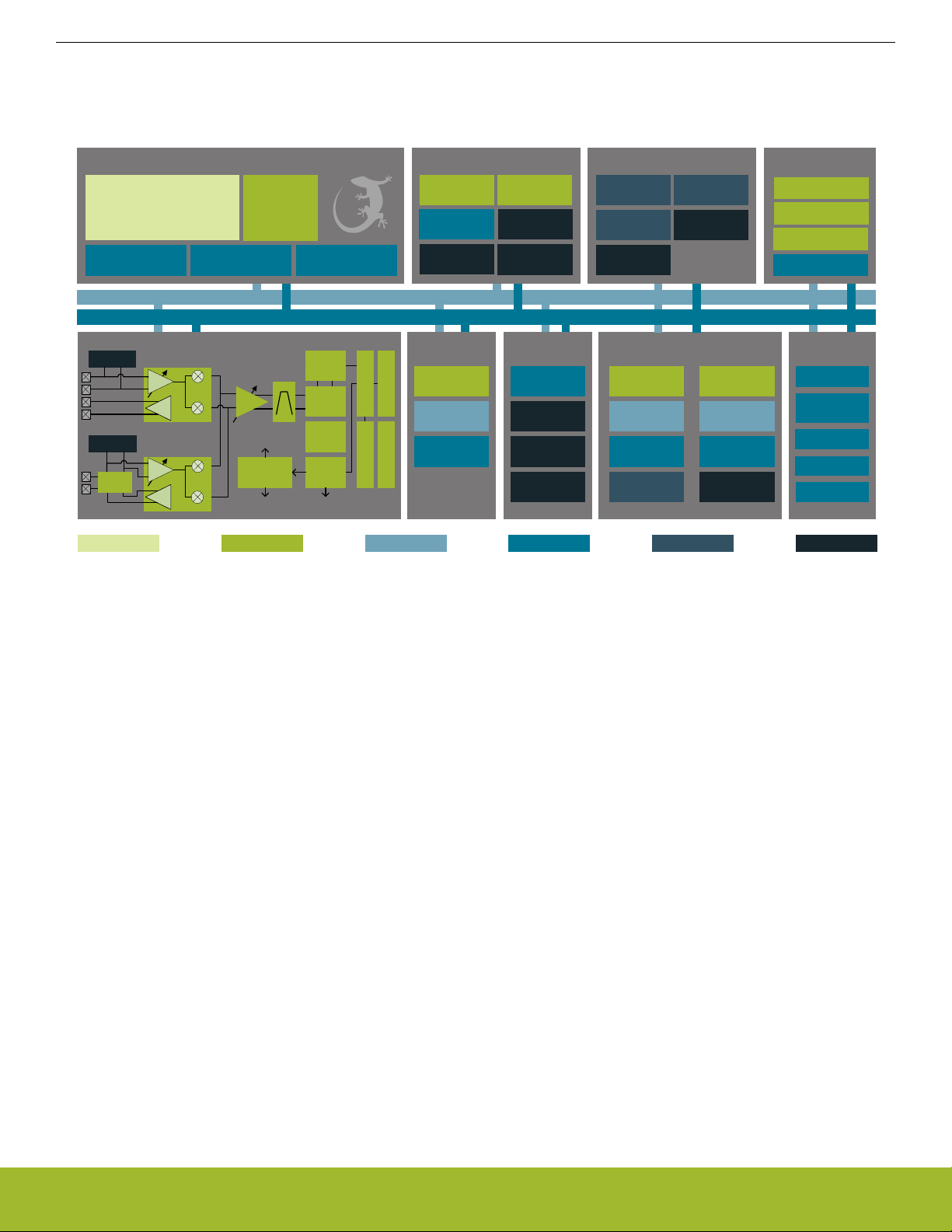
Reference Manual
System Overview
2.2 Block Diagrams
The block diagram for the EFR32 System-On-Chip series is shown in (Figure 2.1 EFR32 System-On-Chip Block Diagram on page
29).
Core / Memory
ARM Cortex
with DSP extensions, FPU and MPU
Debug Interface RAM Memory LDMA Controller
TM
M4 processor
Flash Program
Memory
Radio Transceiver
RFSENSE
RFSENSE
Lowest power mode with peripheral operational:
BALUN
Sub GHz
LNA
RF Frontend
PA
2.4 GHz
LNA
RF Frontend
PA
I
Q
I
Q
PGA
To Sub GHz
receive I/Q
mixers and PA
Frequency
Synthesizer
To 2.4 GHz receive
I/Q mixers and PA
DEMOD
IFADC
AGC
MOD
To Sub GHz
and 2.4 GHz PA
Figure 2.1. EFR32 System-On-Chip Block Diagram
FRC
CRC
Clock Management
H-F Crystal
Oscillator
Auxiliary H-F RC
Oscillator
L-F Crystal
Oscillator
32-bit bus
Peripheral Reflex System
Serial
Interfaces
BUFC
RAC
USART
Low Energy
TM
UART
2
I
C
Energy Management
H-F
RC Oscillator
L-F
RC Oscillator
Ultra L-F RC
Oscillator
I/O Ports Analog I/F
External
Interrupts
General
Purpose I/O
Pin Reset
Pin Wakeup
EM3—StopEM2—Deep SleepEM1—Sleep EM4—Hibernate EM4—ShutoffEM0—Active
Voltage
Regulator
DC-DC
Converter
Brown-Out
Detector
Voltage Monitor
Power-On Reset
Timers and Triggers
Timer/Counter
Low Energy
Timer
Pulse Counter Watchdog Timer
Real Time
Counter and
Calendar
Protocol Timer
Low Energy
Sensor Interface
Cryotimer
Other
CRYPTO
CRC
True Random
Number Generator
SMU
Comparator
ADC
Analog
IDAC
VDAC
Op-Amp
silabs.com | Building a more connected world. Rev. 1.1 | 29
Page 30

Reference Manual
System Overview
2.3 MCU Features Overview
• ARMCortex-M4 CPU platform
• High Performance 32-bit processor @ up to 40 MHz
• Memory Protection Unit
• Wake-up Interrupt Controller
• Flexible Energy Management System
• 5 Energy Modes from EM0 to EM4 provide flexibility between higher performance and low power
• Power routing configurations including DCDC control
• Voltage Monitoring and Brown Out Detection
• State Retention
• Up to 256 KB Flash
• Up to 32 KB RAM
• Up to 31 General Purpose I/O pins
• Configurable push-pull, open-drain, pull-up/down, input filter, drive strength
• Configurable peripheral I/O locations
• 16 asynchronous external interrupts
• Output state retention and wake-up from Shutoff Mode
• 8 Channel DMA Controller
• Alternate/primary descriptors with scatter-gather/ping-pong operation
• 12 Channel Peripheral Reflex System
• Autonomous inter-peripheral signaling enables smart operation in low energy modes
• CRYPTO Advanced Encryption Standard Accelerator
• AES encryption / decryption, with 128 or 256 bit keys
• Multiple AES modes of operation, including Counter (CTR), Galois/Counter Mode (GCM), Cipher Block Chaining (CBC), Cipher
Feedback (CFB) and Output Feedback (OFB).
• Accelerated SHA-1 and SHA-2 (SHA-224 / SHA-256)
• Accelerated Elliptic Curve Cryptography (ECC), with binary or prime fields
• Flexible 256-bit ALU and sequencer
• True Random Number Generator (TRNG)
• General Purpose Cyclic Redundancy Check
• Programmable 16-bit polynomial, fixed 32-bit polynomial
• The General Purpose Cyclic Redundancy Check (GPCRC) module comes in addition to the radio CRC
• Communication Interfaces
• 2 Universal Synchronous/Asynchronous Receiver/Transmitter
• UART/SPI/SmartCard (ISO 7816)/IrDA/I2S
• Triple buffered full/half-duplex operation
• Hardware flow control
• 4-16 data bits
• 1 Low Energy UART
• Autonomous operation with DMA in Deep Sleep Mode
•
1 I2C Interface with SMBus support
• Address recognition in Stop Mode
• Timers/Counters
• 2 16-bit Timer/Counter
• 3 or 4 Compare/Capture/PWM channels
• Dead-Time Insertion on TIMER0
• 1 32-bit Timer/Counter
• 3 or 4 Compare/Capture/PWM channels
• Dead-Time Insertion on WTIMER0
• 16-bit Low Energy Timer
• 32-bit Ultra Low Energy Timer/Counter (CRYOTIMER) for periodic wake-up from any Energy Mode
• 32-bit Real-Time Counter and Calendar
silabs.com | Building a more connected world. Rev. 1.1 | 30
Page 31

• 16+16+32 bit Protocol Timer
• 16-bit Pulse Counter
• Asynchronous pulse counting/quadrature decoding
• 2 Watchdog Timers with dedicated RC oscillator
• Ultra Low Power Precision Analog Peripherals
• 12-bit 1 Msamples/s Analog to Digital Converter
• All APORT input channels available
• On-chip temperature sensor
• Single ended or differential operation
• Conversion tailgating for predictable latency
• 12-bit 500 ksps Digital to Analog Converter
• 2 single ended channels/1 differential channel
• Up to 2 Operational Amplifiers
• Supports rail-to-rail inputs and outputs
• Programmable gain
• Current Digital to Analog Converter
• Source or sink a configurable constant current
• 2 Analog Comparator
• Programmable speed/current
• Analog Port
• Low-Energy Sensor Interface
• Autonomous sensor monitoring in deep sleep mode
• Wide range of supported sensors, including LC sensors and capacitive touch switches
• Ultra Efficient Power-on Reset and Brown-Out Detector
• Debug Interface
• 4-pin Joint Test Action Group (JTAG) interface
• 2-pin serial-wire debug (SWD) interface
Reference Manual
System Overview
silabs.com | Building a more connected world. Rev. 1.1 | 31
Page 32

2.4 Oscillators and Clocks
EFR32 has six different oscillators integrated, as shown in Table 2.1 EFR32 Oscillators on page 32.
Table 2.1. EFR32 Oscillators
Reference Manual
System Overview
Oscillator Frequency Optional? External
Description
components
HFXO 38 MHz - 40 MHz No Crystal High accuracy, low jitter high frequency crystal oscillator. Tun-
able crystal loading capacitors are fully integrated. The HFXO
is required for all types of RF communication to be active.
HFRCO 1 MHz - 38 MHz No - Medium accuracy RC oscillator, typically used for timing dur-
ing startup of the HFXO and as a clock source as long as no
RF communication is active.
AUXHFRCO 1 MHz - 38 MHz No - Medium accuracy RC oscillator, typically used as alternative
clock source for Analog to Digital Converter or Debug Trace.
LFRCO 32768 Hz No - Medium accuracy frequency reference typically used for medi-
um accuracy RTCC timing.
LFXO 32768 Hz Yes Crystal High accuracy frequency reference typically used for high ac-
curacy RTCC timing. Tunable crystal loading capacitors are
fully integrated.
ULFRCO 1000 Hz No - Ultra low frequency oscillator typically used for the watchdog
timer.
The RC oscillators can be calibrated against either of the crystal oscillators in order to compensate for temperature and voltage supply
variations. Hardware support is included to measure the frequency of various oscillators against each other.
Oscillator and clock management is available through the Clock Management Unit (CMU), see section 11. CMU - Clock Management
Unit for details.
2.5 RF Frequency Synthesizer
The Fractional-N RF Frequency Synthesizer (SYNTH) provides a low phase noise LO signal to be used in both receive and transmit
modes.
The capabilities of the SYNTH include:
• High performance, low phase noise
• Fast frequency settling
• Fast and fully automated calibration
• Sub 100 Hz frequency resolution across the supported frequency bands
2.6 Modulation Modes
EFR32 supports a wide range of modulation modes in transmit and receive:
• 2-FSK, 2-GFSK, 4-FSK, 4-GFSK, MSK, GMSK, O-QPSK with half-sine shaping, ASK / OOK, DBPSK TX
• NRZ or Manchester support
• UART mode over air for legacy protocols
• Data rates ranging from 600 bps up to 2 Mbps
• Configurable frequency deviation
• Configurable Direct Sequence Spread Spectrum (DSSS), with spread sequences up to 32 chips encoding up to 4 information bits
• Configurable 4-FSK symbol encoding
silabs.com | Building a more connected world. Rev. 1.1 | 32
Page 33

Reference Manual
System Overview
2.7 Transmit Mode
In transmit mode EFR32 performs the following functionality:
• Automatic PA power ramping during the start and end of a frame transmit
• Programmable output power
• Optional preamble and synchronization word insertion
• Accurate transmit frame timing to support time synchronized radio protocols
• Optional Carrier Sense Multiple Access - Collision Avoidance (CSMA-CA) or Listen Before Talk (LBT) hardware support
• Integrated transmit test modes, as described in 2.17 RF Test Modes
2.8 Receive Mode
In receive mode EFR32 performs the following functionality:
• A single-ended (2.4 GHz) or differential (Sub-GHz) LNA amplifies the input RF signal. The amplified signal is then mixed to a low-IF
signal through the quadrature down-coversion mixer. Further signal filtering is performed before conversion to a digital signal
through the I/Q ADC.
• Digitally configurable receiver bandwidth from 100 Hz to 2.5 MHz
• Timing recovery on received data, including simultaneous support for two different frame synchronization words
• Automatic frequency offset compensation, to compensate for carrier frequency offset between the transmitter and receiver
• Support for a wide range of modulation formats as described in section 2.6 Modulation Modes
2.9 Data Buffering
EFR32 supports buffered transmit and receive modes through its buffer controller (BUFC), with four individually configurable buffers.
The BUFC uses the system RAM as storage, and each buffer can be individually configured with parameters such as:
• Buffer size
• Buffer interrupt thresholds
• Buffer RAM location
• Overflow and underflow detection
In receive mode, data following frame synchronization is moved directly from the demodulator to the buffer storage.
In transmit mode, data following the inserted preamble and synchronization word is moved directly from the buffer storage to the modulator.
2.10 Unbuffered Data Transfer
For most system designs it is recommended to use the data buffering within EFR32 to provide a convenient user interface.
In cases where data buffering within EFR32 is not desired, it is possible to set up direct unbuffered data transfers using a single-pin or
two-pin interface on EFR32. A bit clock output is provided on the Serial Clock (SC) output pin, and a serial bitstream is provided to
EFR32 in a transmit mode and from EFR32 in a receive mode.
In unbuffered data transfer modes the hardware support provided by EFR32 to perform preamble and frame synchronization insertion
in transmit mode and detection in receive mode can still optionally be used.
2.11 Frame Format Support
EFR32 has an extensive support for frame handling in transmit and receive modes, which allows effective handling of even advanced
protocols. The support includes:
• Preamble and frame synchronization inserted into transmitted frames
• Full frame synchronization of received frames
• Simple address matching of received frames in hardware, further configurable address and frame filtering supported through sequencer
• Support for variable length frames
• Automated CRC calculation and verification
• Configurable bit ordering, with the most or least significant bit transmitted and received first
The frame format support is controlled by the Frame Controller (FRC).
silabs.com | Building a more connected world. Rev. 1.1 | 33
Page 34

Reference Manual
System Overview
2.12 Hardware CRC Support
EFR32 supports a configurable CRC generation in transmit and verification in receive mode:
• 8, 16, 24 or 32 bit CRC value
• Configurable polynomial and initialization value
• Optional inversion of CRC value over air
• Configurable CRC byte ordering
• Support for multiple CRC values calculated and verified per transmitted or received frame
• The CRC module is typically controlled by the Frame Controller (FRC) for in-line operations in transmit and receive modes. Alternatively, the CRC module may be accessed directly from software to calculate and verify CRC data.
2.13 Convolutional Encoding / Decoding
EFR32 includes hardware support for convolutional encoding and decoding, for forward error correction (FEC). This feature is performed by the Frame Controller (FRC) module:
• Constraint length configurable up to 7, for the highest robustness
• Configurable puncturing, to achieve rates between 1/2 rate and full rate
• Configurable soft decision or hard decision decoding
• Convolutional coding may be used together with the symbol interleaver to improve robustness against burst errors
2.14 Binary Block Encoding / Decoding
EFR32 includes hardware support for binary block encoding and decoding, both performed real-time in the the transmit and receive
path. This is performed in the Frame Controller (FRC) module:
The block coding works on blocks of up to 16 bits of data and adds parity bits to be capable of single or multiple bit corrections by the
receiver.
• One or more parity bits can be added and verified
• Bit error correction
• Lookup-codes can be used to implement virtually any block coding scheme
silabs.com | Building a more connected world. Rev. 1.1 | 34
Page 35

Reference Manual
System Overview
2.15 Data Encryption and Authentication
EFR32 has hardware support for AES encryption, decryption and authentication modes. These security operations can be performed
on data in RAM or any data buffer, without further CPU intervention. The key size is 128 bits.
AES modes of operations directly supported by the EFR32 hardware are listed in Table 2.2 AES Modes of Operation With Hardware
Support on page 35. In addition to these modes, other modes can also be implemented by using combinations of modes. For exam-
ple, the CCM mode can be implemented using the CTR and CBC-MAC modes in combination.
Table 2.2. AES Modes of Operation With Hardware Support
AES Mode Encryption / Decryption Authentication Comment
ECB Yes - Electronic Code Book
CTR Yes - Counter mode
CCM Yes Yes Counter with CBC-MAC
CCM* Yes Yes CCM with encryption-only and
integrity-only capabilities
GCM Yes Yes Galois Counter Mode
CBC Yes - Cipher Block Chaining
CBC-MAC - Yes Cipher Block Chaining, Mes-
sage Authentication Code
CMAC - Yes Cipher-based MAC
CFB Yes - Cipher Feedback
OFB Yes - Output Feedback
The CRYPTO module can operate directly on data buffers provided by the BUFC module. It is also possible to provide data directly
from the embedded Cortex-M4 or via DMA.
A True Random Number Generator (TRNG) module is also included for additional security. The TRNG is a non-deterministic random
number generator based on a full hardware solution, and is suitable for cryptographic key generation.
silabs.com | Building a more connected world. Rev. 1.1 | 35
Page 36

2.16 Timers
EFR32 includes multiple timers, as can be seen from Table 2.3 EFR32 Timers Overview on page 36.
Table 2.3. EFR32 Timers Overview
Timer Number of instances Typical clock source Overview
Reference Manual
System Overview
RTCC 1 (2) Low frequency (LFXO or
LFRCO)
PROTIMER 1 High frequency (HFXO or
HFRCO)
TIMER 2 High frequency (HFXO or
HFRCO)
WTIMER 2 High frequency (HFXO or
HFRCO)
Systick timer 1 High frequency (HFXO or
HFRCO)
WDOG 1 Low frequency (LFXO, LFRCO
or ULFRCO)
32 bit Real Time Counter and
Calendar, typically used to enable wakeup on compare match.
A second RTC module is used
by the radio software drivers for
accurately timing inactive periods in the radio communication
protocol.
16+16+32 bit Protocol Timer,
typically used to accurately control detailed RF protocol timing
in transmit and receive modes.
16 bit general purpose timer.
32 bit general purpose timer.
32 bit systick timer integrated in
the Cortex-M4. Typically used
as an Operating System timer.
Watch dog timer. Once enabled,
this module must be periodically
accessed. If not, this is considered an error and the EFR32 is
reset in order to recover the
system.
LETIMER 1 Low frequency (LFXO, LFRCO
or ULFRCO)
Low energy general purpose
timer.
Advanced interconnect features allows synchronization between timers. This includes:
• Start / stop any high frequency timer synchronized with the RTCC
• Trigger RSM state transitions based on compare timer compare match, for instance to provide clock cycle accuracy on frame transmit timing
2.17 RF Test Modes
EFR32 supports a wide range of RF test modes typically used for characterization and regulation compliance testing, including:
• Unmodulated carrier transmit
• Modulated carrier transmit, with internal configurable pseudo random data generator
• Continuous data reception for Bit Error Rate (BER) measurements
• Storing of raw receiver data to RAM
• Transmit of raw frequency data from RAM
silabs.com | Building a more connected world. Rev. 1.1 | 36
Page 37

3. System Processor
43210
CM4 Core
Reference Manual
System Processor
Quick Facts
What?
The industry leading Cortex-M4 processor from
ARM is the CPU in the EFR32 devices.
Why?
The ARM Cortex-M4 is designed for exceptionally
short response time, high code density, and high 32bit throughput while maintaining a strict cost and
power consumption budget.
3.1 Introduction
32-bit ALU
Hardware divider
Control Logic DSP extensions
Floating-Point Unit
Instruction Interface Data Interface
NVIC Interface
Single cycle
32-bit multiplier
Thumb & Thumb-2
Decode
Memory Protection Unit
How?
Combined with the ultra low energy peripherals
available in EFR32 devices, the Cortex-M4 processor's Harvard architecture, 3 stage pipeline, single cycle instructions, Thumb-2 instruction set support,
and fast interrupt handling make it perfect for 8-bit,
16-bit, and 32-bit applications.
The ARM Cortex-M4 32-bit RISC processor provides outstanding computational performance and exceptional system response to interrupts while meeting low cost requirements and low power consumption.
The ARM Cortex-M4 implemented is revision r0p1.
silabs.com | Building a more connected world. Rev. 1.1 | 37
Page 38

Reference Manual
System Processor
3.2 Features
• Harvard architecture
• Separate data and program memory buses (No memory bottleneck as in a single bus system)
• 3-stage pipeline
• Thumb-2 instruction set
• Enhanced levels of performance, energy efficiency, and code density
• Single cycle multiply and hardware divide instructions
• 32-bit multiplication in a single cycle
• Signed and unsigned divide operations between 2 and 12 cycles
• Atomic bit manipulation with bit banding
• Direct access to single bits of data
• Two 1MB bit banding regions for memory and peripherals mapping to 32MB alias regions
• Atomic operation, cannot be interrupted by other bus activities
• 1.25 DMIPS/MHz
• Memory Protection Unit
• Up to 8 protected memory regions
• 24 bits System Tick Timer for Real Time OS
• Excellent 32-bit migration choice for 8/16 bit architecture based designs
• Simplified stack-based programmer's model is compatible with traditional ARM architecture and retains the programming simplicity of legacy 8-bit and 16-bit architectures
• Alligned or unaligned data storage and access
• Contiguous storage of data requiring different byte lengths
• Data access in a single core access cycle
• Integrated power modes
• Sleep Now mode for immediate transfer to low power state
• Sleep on Exit mode for entry into low power state after the servicing of an interrupt
• Ability to extend power savings to other system components
• Optimized for low latency, nested interrupts
3.3 Functional Description
For a full functional description of the ARM Cortex-M4 implementation in the EFR32 family, the reader is referred to the ARM Cortex-M4
documentation provided by ARM.
silabs.com | Building a more connected world. Rev. 1.1 | 38
Page 39

3.3.1 Interrupt Operation
Module Cortex-M NVIC
Reference Manual
System Processor
IFS[n] IFC[n]
IEN[n]
SETENA[n]/CLRENA[n]
Interrupt
condition
set clear
IF[n]
Active interrupt
IRQ
set clear
Interrupt
request
SETPEND[n]/CLRPEND[n]
Software generated interrupt
Figure 3.1. Interrupt Operation
The interrupt request (IRQ) lines are connected to the Cortex-M4. Each of these lines (shown in Table 3.1 Interrupt Request Lines (IRQ)
on page 40) is connected to one or more interrupt flags in one or more modules. The interrupt flags are set by hardware on an inter-
rupt condition. It is also possible to set/clear the interrupt flags through the IFS/IFC registers. Each interrupt flag is then qualified with its
own interrupt enable bit (IEN register), before being OR'ed with the other interrupt flags to generate the IRQ. A high IRQ line will set the
corresponding pending bit (can also be set/cleared with the SETPEND/CLRPEND bits in ISPR0/ICPR0) in the Cortex-M4 NVIC. The
pending bit is then qualified with an enable bit (set/cleared with SETENA/CLRENA bits in ISER0/ICER0) before generating an interrupt
request to the core. Figure 3.1 Interrupt Operation on page 39 illustrates the interrupt system. For more information on how the interrupts are handled inside the Cortex-M4, the reader is referred to the ARM Cortex-M4 Technical Reference Manual.
3.3.1.1 Avoiding Extraneous Interrupts
There can be latencies in the system such that clearing an interrupt flag could take longer than leaving an Interrupt Service Routine
(ISR). This can lead to the ISR being re-entered as the interrupt flag has yet to clear immediately after leaving the ISR. To avoid this,
when clearing an interrupt flag at the end of an ISR, the user should execute ARM's Data Synchronization Barrier (DSB) instruction.
Another approach is to clear the interrupt flag immediately after identifying the interrupt source and then service the interrupt as shown
in the pseudo-code below. The ISR typically is sufficiently long to more than cover the few cycles it may take to clear the interrupt status, and also allows the status to be checked for further interrupts before exiting the ISR.
irqXServiceRoutine() {
do {
clearIrqXStatus();
serviceIrqX();
} while(irqXStatusIsActive());
}
3.3.1.2 IFC Read-clear Operation
In addition to the normal interrupt setting and clearing operations via the IFS/IFC registers, there is an additional atomic Read-clear
operation that can be enabled by setting IFCREADCLEAR=1 in the MSC_CTRL register. When enabled, reads of peripheral IFC registers will return the interrupt vector (mirroring the IF register), while at the same time clearing whichever interrupt flags are set. This operation is functionally equivalent to reading the IF register and then writing the result immediately back to the IFC register.
silabs.com | Building a more connected world. Rev. 1.1 | 39
Page 40

3.3.2 Interrupt Request Lines (IRQ)
Table 3.1. Interrupt Request Lines (IRQ)
IRQ # Source(s)
0 EMU
2 WDOG0
3 WDOG1
9 LDMA
10 GPIO_EVEN
11 TIMER0
12 USART0_RX
13 USART0_TX
14 ACMP0
ACMP1
Reference Manual
System Processor
15 ADC0
16 IDAC0
17 I2C0
18 GPIO_ODD
19 TIMER1
20 USART1_RX
21 USART1_TX
22 LEUART0
23 PCNT0
24 CMU
25 MSC
26 CRYPTO0
27 LETIMER0
31 RTCC
33 CRYOTIMER
35 FPUEH
36 SMU
37 WTIMER0
38 VDAC0
39 LESENSE
40 TRNG0
silabs.com | Building a more connected world. Rev. 1.1 | 40
Page 41

4. Memory and Bus System
43210
ARM Cortex-M
DMA Controller
Flash
RAM
Radio
Peripherals
Reference Manual
Memory and Bus System
Quick Facts
What?
A low latency memory system including low energy
Flash and RAM with data retention which makes the
energy modes attractive.
Why?
RAM retention reduces the need for storing data in
Flash and enables frequent use of the ultra low energy modes EM2 Deep Sleep and EM3 Stop.
How?
Low energy and non-volatile Flash memory stores
program and application data in all energy modes
and can easily be reprogrammed in system. Low
leakage RAM with data retention in EM0 Active to
EM3 Stop removes the data restore time penalty,
and the DMA ensures fast autonomous transfers
with predictable response time.
silabs.com | Building a more connected world. Rev. 1.1 | 41
Page 42

Reference Manual
Memory and Bus System
4.1 Introduction
The EFR32 contains an AMBA AHB Bus system to allow bus masters to access the memory mapped address space. A multilayer AHB
bus matrix connects the 5 master bus interfaces to the AHB slaves (Figure 4.1 EFR32 Bus System on page 42). The bus matrix allows several AHB slaves to be accessed simultaneously. An AMBA APB interface is used for the peripherals, which are accessed
through an AHB-to-APB bridge connected to the AHB bus matrix. The 5 AHB bus masters are:
• Cortex-M4 ICode: Used for instruction fetches from Code memory (valid address range: 0x00000000 - 0x1FFFFFFF)
• Cortex-M4 DCode: Used for debug and data access to Code memory (valid address range: 0x00000000 - 0x1FFFFFFF)
• Cortex-M4 System: Used for data and debug access to system space. It can access entire memory space except Code memory
(valid address range: 0x20000000 - 0xFFFFFFFF)
• DMA: Can access the entire memory space except the internal core memory region and the DMEM code region
• Sequencer Code: Used for instruction fetches and data accesses. Instruction fetches still come from data memory. (valid address
range: 0x00000000 - 0x0FFFFFFF, 0x20000000 - 0x3FFFFFFF)
• Sequencer System: Can access entire memory space except internal core memory region and RAM code space (valid address
range: 0x00000000 - 0x0FFFFFFF, 0x20000000 - 0xDFFFFFFF)
• BUFC: Can access general purpose SRAM (valid address range: 0x20000000 - 0x20FFFFFF)
• FRC: Can access general purpose SRAM (valid address range: 0x20000000 - 0x20FFFFFF)
Cortex-M
Sequencer
BUFC
FRC
DMA
ICode
DCode
System
Code
System
AHB Multilayer
Bus Matrix
Flash
RAM0
RAMn
SEQ_RAM
CRYPTO
AHB/APB
Bridge
Figure 4.1. EFR32 Bus System
Peripheral 0
Peripheral n
silabs.com | Building a more connected world. Rev. 1.1 | 42
Page 43

Reference Manual
Memory and Bus System
4.2 Functional Description
The memory segments are mapped together with the internal segments of the Cortex-M4 into the system memory map shown by Fig-
ure 4.2 System Address Space With Core and Code Space Listing on page 43.
Figure 4.2. System Address Space With Core and Code Space Listing
Additionally, the peripheral address map is detailed by Figure 4.3 System Address Space With Peripheral Listing on page 44.
silabs.com | Building a more connected world. Rev. 1.1 | 43
Page 44

Reference Manual
Memory and Bus System
Figure 4.3. System Address Space With Peripheral Listing
The embedded SRAM is located at address 0x20000000 in the memory map of the EFR32. When running code located in SRAM starting at this address, the Cortex-M4 uses the System bus interface to fetch instructions. This results in reduced performance as the Cortex-M4 accesses stack, other data in SRAM and peripherals using the System bus interface. To be able to run code from SRAM efficiently, the SRAM is also mapped in the code space at address 0x10000000.
When running code from this space, the Cortex-M4 fetches instructions through the I/D-Code bus interface, leaving the System bus
interface for data access.
The SRAM mapped into the code space can however only be accessed by the CPU and not any other bus masters, e.g. DMA. See
4.5 SRAM for more detailed info on the system SRAM.
The Sequencer RAM is used by the Sequencer for both instructions and data. This RAM is also available for general use by most AHB
masters.
silabs.com | Building a more connected world. Rev. 1.1 | 44
Page 45

Reference Manual
Memory and Bus System
4.2.1 Peripheral Non-Word Access Behavior
When writing to peripheral registers, all accesses are treated as 32-bit accesses. This means that writes to a register need to be large
enough to cover all bits of register, otherwise, any uncovered bits may become corrupted from the partial-word transfer. Thus, the safest
practice is to always do 32-bit writes to peripheral registers.
When reading, there is generally no issue with partial word accesses, however, note that any read action (e.g. FIFO popping) will be
triggered regardless of whether the actual FIFO bit-field was included in the transfer size.
Note: The implementation of bit-banding in the core is such that bit-band accesses forward the transfer size info into the actual bus
transfer size, so the same restrictions apply to bit-band accesses as apply to normal read/write accesses.
4.2.2 Bit-banding
The SRAM bit-band alias and peripheral bit-band alias regions are located at 0x22000000 and 0x42000000 respectively. Read and
write operations to these regions are converted into masked single-bit reads and atomic single-bit writes to the embedded SRAM and
peripherals of the EFR32.
Note: Bit-banding is only available through the CPU. No other AHB masters (e.g. DMA) can perform Bit-banding operations.
Using a standard approach to modify a single register or SRAM bit in the aliased regions, would require software to read the value of
the byte, half-word or word containing the bit, modify the bit, and then write the byte, half-word or word back to the register or SRAM
address. Using bit-banding, this can be done in a single operation, consuming only two bus cycles. As read-writeback, bit-masking and
bit-shift operations are not necessary in software, code size is reduced and execution speed improved.
The bit-band regions allow each bit in the SRAM and Peripheral areas of the memory map to be addressed. To set or clear a bit in the
embedded SRAM, write a 1 or a 0 to the following address:
bit_address = 0x22000000 + (address – 0x20000000) ∙ 32 + bit ∙ 4
where address is the address of the 32-bit word containing the bit to modify, and bit is the index of the bit in the 32-bit word.
To modify a bit in the Peripheral area, use the following address:
bit_address = 0x42000000 + (address – 0x40000000) ∙ 32 + bit ∙ 4
silabs.com | Building a more connected world. Rev. 1.1 | 45
Page 46

Reference Manual
Memory and Bus System
4.2.3 Peripheral Bit Set and Clear
The EFR32 supports bit set and bit clear access to all peripherals except those listed in Table 4.1 Peripherals that Do Not Support Bit
Set and Bit Clear on page 46. The bit set and bit clear functionality (also called Bit Access) enables modification of bit fields (single bit
or multiple bit wide) without the need to perform a read-modify-write (though it is functionally equivalent). Also, the operation is contained within a single bus access (for HF peripherals), unlike the Bit-banding operation described in section 4.2.2 Bit-banding which
consumes two bus accesses per operation. All AHB masters can utilize this feature.
The bit clear aliasing region starts at 0x44000000 and the bit set aliasing region starts at 0x46000000. Thus, to apply a bit set or clear
operation, write the bit set or clear mask to the following addresses:
bit_clear_address = address + 0x04000000
bit_set_address = address + 0x06000000
For bit set operations, bit locations that are 1 in the bit mask will be set in the destination register:
register = (register OR mask)
For bit clear operations, bit locations that are 1 in the bit mask will be cleared in the destination register:
register = (register AND (NOT mask))
Note: It is possible to combine bit clear and bit set operations in order to arbitrarily modify multi-bit register fields, without affecting other
fields in the same register. In this case, care should be taken to ensure that the field does not have intermediate values that can lead to
erroneous behavior. For example, if bit clear and bit set operations are used to change an analog tuning register field from 25 to 26, the
field would initially take on a value of zero. If the analog module is active at the time, this could lead to undesired behavior.
The peripherals listed in Table 4.1 Peripherals that Do Not Support Bit Set and Bit Clear on page 46 do not support Bit Access for any
registers. All other peripherals do support Bit Access, however, there may be cases of certain registers that do not support it. Such
registers have a note regarding this lack of support.
Table 4.1. Peripherals that Do Not Support Bit Set and Bit Clear
Module
EMU
RMU
CRYOTIMER
TRNG0
silabs.com | Building a more connected world. Rev. 1.1 | 46
Page 47

Reference Manual
Memory and Bus System
4.2.4 Peripherals
The peripherals are mapped into the peripheral memory segment, each with a fixed size address range according to Table 4.2 Periph-
erals on page 47, Table 4.3 Low Energy Peripherals on page 47 , and Table 4.4 Core Peripherals on page 47.
Table 4.2. Peripherals
Address Range Module Name
0x400E6000 - 0x400E6400 PRS
0x40022000 - 0x40022400 SMU
0x4001E000 - 0x4001E400 CRYOTIMER
0x4001D000 - 0x4001D400 TRNG0
0x4001C000 - 0x4001C400 GPCRC
0x4001A000 - 0x4001A400 WTIMER0
0x40018400 - 0x40018800 TIMER1
0x40018000 - 0x40018400 TIMER0
0x40010400 - 0x40010800 USART1
0x40010000 - 0x40010400 USART0
0x4000C000 - 0x4000C400 I2C0
0x4000A000 - 0x4000B000 GPIO
0x40008000 - 0x40008400 VDAC0
0x40006000 - 0x40006400 IDAC0
0x40002000 - 0x40002400 ADC0
0x40000400 - 0x40000800 ACMP1
0x40000000 - 0x40000400 ACMP0
Table 4.3. Low Energy Peripherals
Address Range Module Name
0x40055000 - 0x40055400 LESENSE
0x40052400 - 0x40052800 WDOG1
0x40052000 - 0x40052400 WDOG0
0x4004E000 - 0x4004E400 PCNT0
0x4004A000 - 0x4004A400 LEUART0
0x40046000 - 0x40046400 LETIMER0
0x40042000 - 0x40042400 RTCC
Table 4.4. Core Peripherals
Address Range Module Name
0xE0000000 - 0xE0040000 CM4
0x400F0000 - 0x400F0400 CRYPTO0
silabs.com | Building a more connected world. Rev. 1.1 | 47
Page 48

Reference Manual
Memory and Bus System
Address Range Module Name
0x400E2000 - 0x400E3000 LDMA
0x400E1000 - 0x400E1400 FPUEH
0x400E0000 - 0x400E0800 MSC
4.2.5 Bus Matrix
The Bus Matrix connects the memory segments to the bus masters as detailed in 4.1 Introduction.
4.2.5.1 Arbitration
The Bus Matrix uses a round-robin arbitration algorithm which enables high throughput and low latency, while starvation of simultaneous accesses to the same bus slave are eliminated. Round-robin does not assign a fixed priority to each bus master. The arbiter does
not insert any bus wait-states during peak interaction. However, one wait state is inserted for master accesses occurring after a prolonged inactive time. This wait state allows for increased power efficiency during master idle time.
4.2.5.2 Peripheral Access Performance
The Bus Matrix is a multi-layer energy optimized AMBA AHB compliant bus with an internal bandwidth of 5x a single AHB interface.
The Cortex-M4, DMA Controller, and peripherals (not peripherals in the low frequency clock domain) run on clocks which can be prescaled separately. Clocks and prescaling are described in more detail in 11. CMU - Clock Management Unit . This section describes the
expected bus wait states for a peripheral based on its frequency relative to the HFCLK frequency. For this discussion, PERCLK refers
to a selected peripheral's clock frequency, which is some integer division of the HFCLK frequency.
Another factor that effects the cycle latency of peripheral accesses is the Peripheral Access Wait Mode (WAITMODE in MSC_CTRL)
configuration, which is present in some parts in the EFR32 series. For instance, when set to WS0, a higher throughput (in terms of
HFCLK cycles) is possible than with a higher wait state setting. However, this family of parts does not have configurable wait states.
Instead, refer to the access performance information for WS0 for this device family.
silabs.com | Building a more connected world. Rev. 1.1 | 48
Page 49

Reference Manual
Memory and Bus System
4.2.5.2.1 WS0 Mode
In general, when accessing a peripheral, the latency in number of HFCLK cycles, not including master arbitration, is given by:
where N
slave cycles
N
bus cycles
N
bus cycles
N
bus cycles
N
bus cycles
is the throughput of the slave's bus interface in number of PERCLK cycles per transfer, including any wait cycles
= (N
= (N
= N
= N
slave cycles
slave cycles
slave cycles
slave cycles
+ 1) ∙ f
+ 1) ∙ f
∙ f
HFCLK/fPERCLK
∙ f
HFCLK/fPERCLK
HFCLK/fPERCLK
HFCLK/fPERCLK
, best-case write accesses
+ 1, best-case read accesses
- 1, worst-case write accesses
, worst-case read accesses
introduced by the slave.
Figure 4.4. Bus Access Latency (General Case)
Note that a latency of 1 cycle corresponds to 0 wait states.
Additionally, for back-to-back accesses to the same peripheral, the throughput in number of cycles per transfer is given by:
N
bus cycles
N
bus cycles
= N
= (N
slave cycles
slave cycles
∙ f
HFCLK/fPERCLK
+ 1) ∙ f
HFCLK/fPERCLK
, write accesses
, read accesses
Figure 4.5. Bus Access Throughput (Back-to-Back Transfers)
Lastly, in the highest performing case, where PERCLK equals HFCLK and the slave does not introduce any additional wait states, the
access latency in number of cycles is given by:
N
bus cycles
= 1, write accesses
N
bus cycles
= 2, read accesses
Figure 4.6. Bus Access Latency (Max Performance)
silabs.com | Building a more connected world. Rev. 1.1 | 49
Page 50

Reference Manual
Memory and Bus System
4.2.5.2.2 WS1 Mode
In general, when accessing a peripheral, the latency in number of HFCLK cycles, not including master arbitration, is given by:
where N
slave cycles
N
bus cycles
N
bus cycles
N
bus cycles
N
bus cycles
is the throughput of the slave's bus interface in number of PERCLK cycles per transfer, including any wait cycles
= (N
= (N
= N
slave cycles
= N
slave cycles
slave cycles
slave cycles
∙ f
HFCLK/fPERCLK
∙ f
HFCLK/fPERCLK
+ 1) ∙ f
+ 1) ∙ f
HFCLK/fPERCLK
HFCLK/fPERCLK
+ 2, best-case write accesses
+ 1, best-case read accesses
+ 1, worst-case write accesses
, worst-case read accesses
introduced by the slave.
Figure 4.7. Bus Access Latency (General Case)
Note that a latency of 1 cycle corresponds to 0 wait states.
Additionally, for back-to-back accesses to the same peripheral, the throughput in number of cycles per transfer is given by:
N
bus cycles
= max{f
N
bus cycles
HFCLK/fPERCLK
= (N
, 2} + N
slave cycles
slave cycles
+ 1) ∙ f
∙ f
HFCLK/fPERCLK
HFCLK/fPERCLK
, write accesses
, read accesses
Figure 4.8. Bus Access Throughput (Back-to-Back Transfers)
Lastly, in the highest performing case, where PERCLK equals HFCLK and the slave does not introduce any additional wait states, the
access latency in number of cycles is given by:
N
bus cycles
= 3, write accesses
N
bus cycles
= 2, read accesses
Figure 4.9. Bus Access Latency (Max Performance)
4.2.5.2.3 Core Access Latency
Note that the cycle counts in the equations above is in terms of the HFCLK. When the core is prescaled from the bus clock, the core will
see a reduced number of latency cycles given by:
N
core cycles
= ceiling( N
bus cycles
∙ f
HFCORECLK/fHFCLK
)
where master arbitration is not included.
Figure 4.10. Core Access Latency
silabs.com | Building a more connected world. Rev. 1.1 | 50
Page 51

Reference Manual
Memory and Bus System
4.2.5.3 Bus Faults
System accesses from the core can receive a bus fault in the following condition(s):
• The core attempts to access an address that is not assigned to any peripheral or other system device. These faults can be enabled
or disabled by setting the ADDRFAULTEN bit appropriately in MSC_CTRL.
• The core attempts to access a peripheral or system device that has its clock disabled. These faults can be enabled or disabled by
setting the CLKDISFAULTEN bit appropriately in MSC_CTRL.
• The bus times out during an access. For example, this could happen while trying to synchronize volatile read data during an LE
peripheral access. See 11.3.1.1 HFCLK - High Frequency Clock. These faults can be enabled or disabled by setting the TIMEOUTFAULTEN bit appropriately in MSC_CTRL.
In addition to any condition-specific bus fault control bits, the bus fault interrupt itself can be enabled or disabled in the same way as all
other internal core interrupts.
Note: The icache flush is not triggered at the event of a bus fault. As a result, when an instruction fetch results in a bus fault, invalid
data may be cached. This means that the next time the instruction that caused the bus fault is fetched, the processor core will get the
invalid cached data without any bus fault. In order to avoid invalid cached data propagation to the processor core, software should manually invalidate cache by writing 1 to MSC_CMD_INVCACHE bitfield at the event of a bus fault.
4.3 Access to Low Energy Peripherals (Asynchronous Registers)
The Low Energy Peripherals are capable of running when the high frequency oscillator and core system is powered off, i.e. in energy
mode EM2 Deep Sleep and in some cases also EM3 Stop. This enables the peripherals to perform tasks while the system energy consumption is minimal.
The Low Energy Peripherals are listed in Table 4.3 Low Energy Peripherals on page 47.
All Low Energy Peripherals are memory mapped, with automatic data synchronization. Because the Low Energy Peripherals are running on clocks asynchronous to the high frequency system clock, there are some constraints on how register accesses are performed,
as described in the following sections.
silabs.com | Building a more connected world. Rev. 1.1 | 51
Page 52

Reference Manual
Memory and Bus System
4.3.1 Writing
Every Low Energy Peripheral has one or more registers with data that needs to be synchronized into the Low Energy clock domain to
maintain data consistency and predictable operation. There are two different synchronization mechanisms on the EFR32, immediate
synchronization, and delayed synchronization. Immediate synchronization is available for the RTCC, LESENSE and LETIMER, and results in an immediate update of the target registers. Delayed synchronization is used for the remaining Low Energy Peripherals, and for
these peripherals, a write operation requires 3 positive edges of the clock on the Low Energy Peripheral being accessed. Registers
requiring synchronization are marked "Async Reg" in their description header.
Note: On the Gecko series of devices, all LE peripherals are subject to delayed synchronization.
Write request [0:n]
High Frequency Clock Domain
High Frequency Clock
Write request 0
Write request 1
Write request n
Set 0
Set 1
Set n
Register 0
Register 1
.
.
.
Register n
Syncbusy Register 0
Syncbusy Register 1
.
.
.
Syncbusy Register n
Figure 4.11. Write Operation to Low Energy Peripherals
Clear 0
Clear 1
Clear n
Freeze
Low Frequency Clock Domain
Low Frequency Clock Low Frequency Clock
Synchronizer 0
Synchronizer 1
.
.
.
Synchronizer n
Synchronization Done
Register 0 Sync
Register 1 Sync
Register n Sync
.
.
.
silabs.com | Building a more connected world. Rev. 1.1 | 52
Page 53

Reference Manual
Memory and Bus System
4.3.1.1 Delayed Synchronization
After writing data to a register which value is to be synchronized into the Low Energy Peripheral using delayed synchronization, a corresponding busy flag in the <module_name>_SYNCBUSY register (e.g. LETIMER_SYNCBUSY) is set. This flag is set as long as synchronization is in progress and is cleared upon completion.
Note: Subsequent writes to the same register before the corresponding busy flag is cleared is not supported. Write before the busy flag
is cleared may result in undefined behavior. In general the SYNCBUSY register only needs to be observed if there is a risk of multiple
write access to a register (which must be prevented). It is not required to wait until the relevant flag in the SYNCBUSY register is
cleared after writing a register. E.g., EM2 Deep Sleep can be entered directly after writing a register.
See Figure 4.12 Write Operation to Low Energy Peripherals on page 53 for an overview of the writing mechanism operation.
Write request [0:n]
High Frequency Clock Domain
High Frequency Clock
Write request 0
Write request 1
Write request n
Set 0
Set 1
Set n
Register 0
Register 1
.
.
.
Register n
Syncbusy Register 0
Syncbusy Register 1
.
.
.
Syncbusy Register n
Freeze
Clear 0
Clear 1
Clear n
Low Frequency Clock Domain
Low Frequency Clock Low Frequency Clock
Synchronizer 0
Synchronizer 1
.
.
.
Synchronizer n
Synchronization Done
Register 0 Sync
Register 1 Sync
Register n Sync
.
.
.
Figure 4.12. Write Operation to Low Energy Peripherals
4.3.1.2 Immediate Synchronization
In contrast to the peripherals with delayed synchronization, peripherals with immediate synchronization do not experience a delay from
a value is written to it takes effect in the peripheral. They are updated immediately on the peripheral write access. If such a write is done
close to an edge on the clock of the peripheral, the write is delayed to after the clock edge. This will introduce wait-states on the peripheral access.
Peripherals with immediate synchronization each have a SYNCBUSY register. Commands written to a peripheral with immediate synchronization are not executed before the first peripheral clock after the write. In this period, the SYNCBUSY flag for the command register is set, indicating that the command has not yet been performed. Secondly, to maintain compatibility with the Gecko series, the rest
of the SYNCBUSY registers are also present, but these are always 0, indicating that register writes are always safe.
Note: If compatibility with the Gecko series is a requirement for a given application, the rules that apply to delayed synchronization with
respect to SYNCBUSY should also be followed for the peripherals that support immediate synchronization.
silabs.com | Building a more connected world. Rev. 1.1 | 53
Page 54

Reference Manual
Memory and Bus System
4.3.2 Reading
When reading from a Low Energy Peripheral, the data read is synchronized regardless if it originates in the Low Energy clock domain
or High Frequency clock domain. See Figure 4.13 Read Operation From Low Energy Peripherals on page 54 for an overview of the
reading operation.
Note: Writing a register and then immediately reading the new value of the register may give the impression that the write operation is
complete. This may not be the case. Refer to the SYNCBUSY register for correct status of the write operation to the Low Energy Peripheral.
High Frequency Clock Domain Low Frequency Clock Domain
High Frequency Clock
Freeze
Low Frequency Clock Low Frequency Clock
Register 0
Register 1
.
.
.
Register n
Read
Synchronizer
Read Data
Synchronizer 0
Synchronizer 1
.
.
.
Synchronizer n
HW Status Register 0
HW Status Register 1
.
.
.
HW Status Register m
Register 0 Sync
Register 1 Sync
.
.
.
Register n Sync
Low Energy
Peripheral
Main
Function
Figure 4.13. Read Operation From Low Energy Peripherals
4.3.3 FREEZE Register
In all Low Energy Peripheral with delayed synchronization there is a <module_name>_FREEZE register (e.g. RTCC_FREEZE). The
register contains a bit named REGFREEZE. If precise control of the synchronization process is required, this bit may be utilized. When
REGFREEZE is set, the synchronization process is halted allowing the software to write multiple Low Energy registers before starting
the synchronization process, thus providing precise control of the module update process. The synchronization process is started by
clearing the REGFREEZE bit.
Note: The FREEZE register is also present on peripherals with immediate synchronization, but there it has no effect
4.4 Flash
The Flash retains data in any state and typically stores the application code, special user data and security information. The Flash
memory is typically programmed through the debug interface, but can also be erased and written to from software.
• Up to 256 KB of memory
• Page size of 2 KB (minimum erase unit)
• Minimum 10K erase cycles endurance
• Greater than 10 years data retention at 85 °C
• Lock-bits for memory protection
• Data retention in any state
silabs.com | Building a more connected world. Rev. 1.1 | 54
Page 55

Reference Manual
Memory and Bus System
4.5 SRAM
The primary task of the SRAM memory is to store application data. Additionally, it is possible to execute instructions from SRAM, and
the DMA may be set up to transfer data between the SRAM, Flash and peripherals.
• Up to 32 KB of memory
• Bit-band access support
• Set of RAM blocks may be powered down when not in use
• Data retention of the entire memory in EM0 Active to EM3 Stop
Note: The individual RAM sections may be smaller on some parts, however, the RAM AHB slaves maintain a contiguous address map.
For example, if RAM0 is half-size on a part, then RAM1 is relocated to begin immediately after RAM0's last address. Using the provided
software header files and linker scripts allows handling of this remapping in an autonomous manner.
silabs.com | Building a more connected world. Rev. 1.1 | 55
Page 56

Reference Manual
Memory and Bus System
4.6 DI Page Entry Map
The DI page contains production calibration data as well as device identification information. See the peripheral chapters for how each
calibration value is to be used with the associated peripheral.
The offset address is relative to the start address of the DI page (see 7.3 Functional Description).
Offset Name Type Description
0x000 CAL RO CRC of DI-page and calibration temperature
0x020 EXTINFO RO External Component description
0x028 EUI48L RO EUI48 OUI and Unique identifier
0x02C EUI48H RO OUI
0x030 CUSTOMINFO RO Custom information
0x034 MEMINFO RO Flash page size and misc. chip information
0x040 UNIQUEL RO Low 32 bits of device unique number
0x044 UNIQUEH RO High 32 bits of device unique number
0x048 MSIZE RO Flash and SRAM Memory size in kB
0x04C PART RO Part description
0x050 DEVINFOREV RO Device information page revision
0x054 EMUTEMP RO EMU Temperature Calibration Information
0x060 ADC0CAL0 RO ADC0 calibration register 0
0x064 ADC0CAL1 RO ADC0 calibration register 1
0x068 ADC0CAL2 RO ADC0 calibration register 2
0x06C ADC0CAL3 RO ADC0 calibration register 3
0x080 HFRCOCAL0 RO HFRCO Calibration Register (4 MHz)
0x08C HFRCOCAL3 RO HFRCO Calibration Register (7 MHz)
0x098 HFRCOCAL6 RO HFRCO Calibration Register (13 MHz)
0x09C HFRCOCAL7 RO HFRCO Calibration Register (16 MHz)
0x0A0 HFRCOCAL8 RO HFRCO Calibration Register (19 MHz)
0x0A8 HFRCOCAL10 RO HFRCO Calibration Register (26 MHz)
0x0AC HFRCOCAL11 RO HFRCO Calibration Register (32 MHz)
0x0B0 HFRCOCAL12 RO HFRCO Calibration Register (38 MHz)
0x0E0 AUXHFRCOCAL0 RO AUXHFRCO Calibration Register (4 MHz)
0x0EC AUXHFRCOCAL3 RO AUXHFRCO Calibration Register (7 MHz)
0x0F8 AUXHFRCOCAL6 RO AUXHFRCO Calibration Register (13 MHz)
0x0FC AUXHFRCOCAL7 RO AUXHFRCO Calibration Register (16 MHz)
0x100 AUXHFRCOCAL8 RO AUXHFRCO Calibration Register (19 MHz)
0x108 AUXHFRCOCAL10 RO AUXHFRCO Calibration Register (26 MHz)
0x10C AUXHFRCOCAL11 RO AUXHFRCO Calibration Register (32 MHz)
0x110 AUXHFRCOCAL12 RO AUXHFRCO Calibration Register (38 MHz)
0x140 VMONCAL0 RO VMON Calibration Register 0
silabs.com | Building a more connected world. Rev. 1.1 | 56
Page 57

Offset Name Type Description
0x144 VMONCAL1 RO VMON Calibration Register 1
0x148 VMONCAL2 RO VMON Calibration Register 2
0x158 IDAC0CAL0 RO IDAC0 Calibration Register 0
0x15C IDAC0CAL1 RO IDAC0 Calibration Register 1
0x168 DCDCLNVCTRL0 RO DCDC Low-noise VREF Trim Register 0
0x16C DCDCLPVCTRL0 RO DCDC Low-power VREF Trim Register 0
0x170 DCDCLPVCTRL1 RO DCDC Low-power VREF Trim Register 1
0x174 DCDCLPVCTRL2 RO DCDC Low-power VREF Trim Register 2
0x178 DCDCLPVCTRL3 RO DCDC Low-power VREF Trim Register 3
0x17C DCDCLPCMPHYSSEL0 RO DCDC LPCMPHYSSEL Trim Register 0
0x180 DCDCLPCMPHYSSEL1 RO DCDC LPCMPHYSSEL Trim Register 1
0x184 VDAC0MAINCAL RO VDAC0 Cals for Main Path
0x188 VDAC0ALTCAL RO VDAC0 Cals for Alternate Path
Reference Manual
Memory and Bus System
0x18C VDAC0CH1CAL RO VDAC0 CH1 Error Cal
0x190 OPA0CAL0 RO OPA0 Calibration Register for DRIVESTRENGTH 0, INCBW=1
0x194 OPA0CAL1 RO OPA0 Calibration Register for DRIVESTRENGTH 1, INCBW=1
0x198 OPA0CAL2 RO OPA0 Calibration Register for DRIVESTRENGTH 2, INCBW=1
0x19C OPA0CAL3 RO OPA0 Calibration Register for DRIVESTRENGTH 3, INCBW=1
0x1A0 OPA1CAL0 RO OPA1 Calibration Register for DRIVESTRENGTH 0, INCBW=1
0x1A4 OPA1CAL1 RO OPA1 Calibration Register for DRIVESTRENGTH 1, INCBW=1
0x1A8 OPA1CAL2 RO OPA1 Calibration Register for DRIVESTRENGTH 2, INCBW=1
0x1AC OPA1CAL3 RO OPA1 Calibration Register for DRIVESTRENGTH 3, INCBW=1
0x1D0 OPA0CAL4 RO OPA0 Calibration Register for DRIVESTRENGTH 0, INCBW=0
0x1D4 OPA0CAL5 RO OPA0 Calibration Register for DRIVESTRENGTH 1, INCBW=0
0x1D8 OPA0CAL6 RO OPA0 Calibration Register for DRIVESTRENGTH 2, INCBW=0
0x1DC OPA0CAL7 RO OPA0 Calibration Register for DRIVESTRENGTH 3, INCBW=0
0x1E0 OPA1CAL4 RO OPA1 Calibration Register for DRIVESTRENGTH 0, INCBW=0
0x1E4 OPA1CAL5 RO OPA1 Calibration Register for DRIVESTRENGTH 1, INCBW=0
0x1E8 OPA1CAL6 RO OPA1 Calibration Register for DRIVESTRENGTH 2, INCBW=0
0x1EC OPA1CAL7 RO OPA1 Calibration Register for DRIVESTRENGTH 3, INCBW=0
silabs.com | Building a more connected world. Rev. 1.1 | 57
Page 58

4.7 DI Page Entry Description
4.7.1 CAL - CRC of DI-page and calibration temperature
Offset Bit Position
Reference Manual
Memory and Bus System
0x000
Access
31
30
29
28
27
26
25
24
23
22
21
20
RO
19
18
17
16
15
14
13
12
11
10
9
8
7
6
5
4
3
RO
Name
TEMP
CRC
Bit Name Access Description
31:24 Reserved Reserved for future use
23:16 TEMP RO Calibration temperature as an usigned int in DegC (25 =
25DegC)
15:0 CRC RO CRC of DI-page (CRC-16-CCITT)
2
1
0
silabs.com | Building a more connected world. Rev. 1.1 | 58
Page 59

4.7.2 EXTINFO - External Component description
Offset Bit Position
Reference Manual
Memory and Bus System
0x020
Access
31
30
29
28
27
26
25
24
23
22
21
20
RO
19
18
17
16
15
14
13
12
11
RO
10
9
8
7
Name
REV
CONNECTION
Bit Name Access Description
31:24 Reserved Reserved for future use
23:16 REV RO MCM Revision
Value Mode Description
1 REV1 Revision 1
255 NONE No external component present
15:8 CONNECTION RO Connection protocal to external interface
Value Mode Description
6
5
4
3
2
1
0
RO
TYPE
1 SPI SPI control interface
255 NONE None
7:0 TYPE RO
External Component
Value Mode Description
1 IS25LQ040B IS25LQ040B-JWLE1 512kB Serial Flash
2 AT25S041 AT25S041-DWFHT 512kB Serial Flash
255 NONE None
silabs.com | Building a more connected world. Rev. 1.1 | 59
Page 60

4.7.3 EUI48L - EUI48 OUI and Unique identifier
Offset Bit Position
Reference Manual
Memory and Bus System
0x028
Access
31
30
29
28
RO
27
26
25
24
23
22
21
20
19
18
17
16
15
14
13
12
11
RO
10
9
8
7
6
5
4
Name
OUI48L
UNIQUEID
Bit Name Access Description
31:24 OUI48L RO Lower Octet of EUI48 Organizationally Unique Identifier
23:0 UNIQUEID RO Unique identifier
4.7.4 EUI48H - OUI
Offset Bit Position
0x02C
Access
31
30
29
28
27
26
25
24
23
22
21
20
19
18
17
16
15
14
13
12
11
10
9
8
7
6
5
4
RO
3
2
1
0
3
2
1
0
Name
OUI48H
Bit Name Access Description
31:16 Reserved Reserved for future use
15:0 OUI48H RO Upper two Octets of EUI48 Organizationally Unique Identifier
4.7.5 CUSTOMINFO - Custom information
Offset Bit Position
0x030
Access
31
30
29
28
27
26
25
24
RO
23
22
21
20
19
18
17
16
15
14
13
12
11
10
9
8
7
6
5
4
3
2
Name
PARTNO
Bit Name Access Description
31:16 PARTNO RO Custom part identifier as unsigned integer (e.g. 903) 65535 for
standard product
1
0
15:0 Reserved Reserved for future use
silabs.com | Building a more connected world. Rev. 1.1 | 60
Page 61

4.7.6 MEMINFO - Flash page size and misc. chip information
Offset Bit Position
Reference Manual
Memory and Bus System
0x034
Access
31
30
29
28
RO
27
26
25
24
23
22
21
20
RO
19
18
17
16
15
14
13
12
11
RO
10
9
8
7
6
5
Name
FLASH_PAGE_SIZE
PINCOUNT
PKGTYPE
Bit Name Access Description
31:24 FLASH_PAGE_SIZE RO Flash page size in bytes coded as 2 ^ ((MEM_IN-
FO_PAGE_SIZE + 10) & 0xFF). Ie. the value 0xFF = 512 bytes.
23:16 PINCOUNT RO Device pin count as unsigned integer (eg. 48)
15:8 PKGTYPE RO Package Identifier as character
Value Mode Description
4
3
2
RO
TEMPGRADE
1
0
74 WLCSP WLCSP package
76 BGA BGA package
77 QFN QFN package
81 QFP QFP package
7:0 TEMPGRADE RO Temperature Grade of product as unsigned integer enumeration
Value Mode Description
0 N40TO85 -40 to 85degC
1 N40TO125 -40 to 125degC
2 N40TO105 -40 to 105degC
3 N0TO70 0 to 70degC
silabs.com | Building a more connected world. Rev. 1.1 | 61
Page 62

4.7.7 UNIQUEL - Low 32 bits of device unique number
Offset Bit Position
Reference Manual
Memory and Bus System
0x040
Access
31
30
29
28
27
26
25
24
23
22
21
20
19
18
17
16
RO
15
14
13
12
11
10
9
8
Name
UNIQUEL
Bit Name Access Description
31:0 UNIQUEL RO Low 32 bits of device unique number
4.7.8 UNIQUEH - High 32 bits of device unique number
Offset Bit Position
0x044
Access
31
30
29
28
27
26
25
24
23
22
21
20
19
18
17
16
RO
15
14
13
12
11
10
9
8
Name
UNIQUEH
7
6
5
4
3
2
1
0
7
6
5
4
3
2
1
0
Bit Name Access Description
31:0 UNIQUEH RO High 32 bits of device unique number
4.7.9 MSIZE - Flash and SRAM Memory size in kB
Offset Bit Position
0x048
Access
31
30
29
28
27
26
25
24
RO
23
22
21
20
19
18
17
16
15
14
13
12
11
10
9
8
7
6
5
4
RO
Name
SRAM
FLASH
Bit Name Access Description
31:16 SRAM RO Ram size, kbyte count as unsigned integer (eg. 16)
15:0 FLASH RO Flash size, kbyte count as unsigned integer (eg. 128)
3
2
1
0
silabs.com | Building a more connected world. Rev. 1.1 | 62
Page 63

4.7.10 PART - Part description
Offset Bit Position
Reference Manual
Memory and Bus System
0x04C
Access
31
30
29
28
RO
27
26
25
24
23
22
21
20
RO
19
18
17
16
15
14
13
12
11
10
9
8
7
RO
Name
PROD_REV
DEVICE_FAMILY
DEVICE_NUMBER
Bit Name Access Description
31:24 PROD_REV RO Production revision as unsigned integer
23:16 DEVICE_FAMILY RO Device Family
Value Mode Description
16 EFR32MG1P EFR32 Mighty Gecko Family Series 1 Device Config 1
17 EFR32MG1B EFR32 Mighty Gecko Family Series 1 Device Config 1
18 EFR32MG1V EFR32 Mighty Gecko Family Series 1 Device Config 1
6
5
4
3
2
1
0
19 EFR32BG1P EFR32 Blue Gecko Family Series 1 Device Config 1
20 EFR32BG1B EFR32 Blue Gecko Family Series 1 Device Config 1
21 EFR32BG1V EFR32 Blue Gecko Family Series 1 Device Config 1
25 EFR32FG1P EFR32 Flex Gecko Family Series 1 Device Config 1
26 EFR32FG1B EFR32 Flex Gecko Family Series 1 Device Config 1
27 EFR32FG1V EFR32 Flex Gecko Family Series 1 Device Config 1
28 EFR32MG12P EFR32 Mighty Gecko Family Series 1 Device Config 2
29 EFR32MG12B EFR32 Mighty Gecko Family Series 1 Device Config 2
30 EFR32MG12V EFR32 Mighty Gecko Family Series 1 Device Config 2
31 EFR32BG12P EFR32 Blue Gecko Family Series 1 Device Config 2
32 EFR32BG12B EFR32 Blue Gecko Family Series 1 Device Config 2
33 EFR32BG12V EFR32 Blue Gecko Family Series 1 Device Config 2
37 EFR32FG12P EFR32 Flex Gecko Family Series 1 Device Config 2
38 EFR32FG12B EFR32 Flex Gecko Family Series 1 Device Config 2
39 EFR32FG12V EFR32 Flex Gecko Family Series 1 Device Config 2
40 EFR32MG13P EFR32 Mighty Gecko Family Series 1 Device Config 3
41 EFR32MG13B EFR32 Mighty Gecko Family Series 1 Device Config 3
42 EFR32MG13V EFR32 Mighty Gecko Family Series 1 Device Config 3
43 EFR32BG13P EFR32 Blue Gecko Family Series 1 Device Config 3
44 EFR32BG13B EFR32 Blue Gecko Family Series 1 Device Config 3
silabs.com | Building a more connected world. Rev. 1.1 | 63
Page 64

Bit Name Access Description
45 EFR32BG13V EFR32 Blue Gecko Family Series 1 Device Config 3
49 EFR32FG13P EFR32 Flex Gecko Family Series 1 Device Config 3
50 EFR32FG13B EFR32 Flex Gecko Family Series 1 Device Config 3
51 EFR32FG13V EFR32 Flex Gecko Family Series 1 Device Config 3
52 EFR32MG14P EFR32 Mighty Gecko Family Series 1 Device Config 4
53 EFR32MG14B EFR32 Mighty Gecko Family Series 1 Device Config 4
54 EFR32MG14V EFR32 Mighty Gecko Family Series 1 Device Config 4
55 EFR32BG14P EFR32 Blue Gecko Family Series 1 Device Config 4
56 EFR32BG14B EFR32 Blue Gecko Family Series 1 Device Config 4
57 EFR32BG14V EFR32 Blue Gecko Family Series 1 Device Config 4
61 EFR32FG14P EFR32 Flex Gecko Family Series 1 Device Config 4
62 EFR32FG14B EFR32 Flex Gecko Family Series 1 Device Config 4
63 EFR32FG14V EFR32 Flex Gecko Family Series 1 Device Config 4
Reference Manual
Memory and Bus System
71 EFM32G EFM32 Gecko Device Family
71 G EFM32 Gecko Device Family
72 EFM32GG EFM32 Giant Gecko Device Family
72 GG EFM32 Giant Gecko Device Family
73 TG EFM32 Tiny Gecko Device Family
73 EFM32TG EFM32 Tiny Gecko Device Family
74 EFM32LG EFM32 Leopard Gecko Device Family
74 LG EFM32 Leopard Gecko Device Family
75 EFM32WG EFM32 Wonder Gecko Device Family
75 WG EFM32 Wonder Gecko Device Family
76 ZG EFM32 Zero Gecko Device Family
76 EFM32ZG EFM32 Zero Gecko Device Family
77 HG EFM32 Happy Gecko Device Family
77 EFM32HG EFM32 Happy Gecko Device Family
81 EFM32PG1B EFM32 Pearl Gecko Family Series 1 Device Config 1
83 EFM32JG1B EFM32 Jade Gecko Family Series 1 Device Config 1
85 EFM32PG12B EFM32 Pearl Gecko Family Series 1 Device Config 2
87 EFM32JG12B EFM32 Jade Gecko Family Series 1 Device Config 2
100 EFM32GG11B EFM32 Giant Gecko Family Series 1 Device Config 1
103 EFM32TG11B EFM32 Tiny Gecko Family Series 1 Device Config 1
120 EZR32LG EZR32 Leopard Gecko Device Family
121 EZR32WG EZR32 Wonder Gecko Device Family
122 EZR32HG EZR32 Happy Gecko Device Family
silabs.com | Building a more connected world. Rev. 1.1 | 64
Page 65

Memory and Bus System
Bit Name Access Description
15:0 DEVICE_NUMBER RO Part number as unsigned integer (e.g. 233 for
EFR32BG1P233F256GM48-B0)
4.7.11 DEVINFOREV - Device information page revision
Offset Bit Position
Reference Manual
0x050
Access
31
30
29
28
27
26
25
24
23
22
21
20
19
18
17
16
15
14
13
12
11
10
9
8
7
6
5
4
3
RO
Name
DEVINFOREV
Bit Name Access Description
31:8 Reserved Reserved for future use
7:0 DEVINFOREV RO DEVINFO layout revision as unsigned integer (initially 1)
4.7.12 EMUTEMP - EMU Temperature Calibration Information
Offset Bit Position
0x054
Access
31
30
29
28
27
26
25
24
23
22
21
20
19
18
17
16
15
14
13
12
11
10
9
8
7
6
5
4
3
RO
2
1
0
2
1
0
Name
EMUTEMPROOM
Bit Name Access Description
31:8 Reserved Reserved for future use
7:0 EMUTEMPROOM RO EMU_TEMP temperature reading at room
silabs.com | Building a more connected world. Rev. 1.1 | 65
Page 66

4.7.13 ADC0CAL0 - ADC0 calibration register 0
Offset Bit Position
Reference Manual
Memory and Bus System
0x060
Access
31
30
29
28
27
RO
26
25
24
23
22
RO
21
20
19
18
RO
17
16
15
14
13
12
11
RO
10
9
8
7
6
5
RO
Name
GAIN2V5
NEGSEOFFSET2V5
OFFSET2V5
GAIN1V25
NEGSEOFFSET1V25
Bit Name Access Description
31 Reserved Reserved for future use
30:24 GAIN2V5 RO Gain for 2.5V reference
23:20 NEGSEOFFSET2V5 RO Negative single ended offset for 2.5V reference
19:16 OFFSET2V5 RO Offset for 2.5V reference
15 Reserved Reserved for future use
4
3
2
1
0
RO
OFFSET1V25
14:8 GAIN1V25 RO Gain for 1.25V reference
7:4 NEGSEOFFSET1V25 RO Negative single ended offset for 1.25V reference
3:0 OFFSET1V25 RO Offset for 1.25V reference
silabs.com | Building a more connected world. Rev. 1.1 | 66
Page 67

4.7.14 ADC0CAL1 - ADC0 calibration register 1
Offset Bit Position
Reference Manual
Memory and Bus System
0x064
Access
31
30
29
28
27
RO
26
25
24
23
22
RO
21
20
19
18
RO
17
16
15
14
13
12
11
RO
10
9
8
7
6
5
4
3
2
RO
RO
Name
GAIN5VDIFF
NEGSEOFFSET5VDIFF
OFFSET5VDIFF
GAINVDD
NEGSEOFFSETVDD
OFFSETVDD
Bit Name Access Description
31 Reserved Reserved for future use
30:24 GAIN5VDIFF RO Gain for for 5V differential reference
23:20 NEGSEOFFSET5VDIFF RO Negative single ended offset with for 5V differential reference
19:16 OFFSET5VDIFF RO Offset for 5V differential reference
1
0
15 Reserved Reserved for future use
14:8 GAINVDD RO Gain for VDD reference
7:4 NEGSEOFFSETVDD RO Negative single ended offset for VDD reference
3:0 OFFSETVDD RO Offset for VDD reference
silabs.com | Building a more connected world. Rev. 1.1 | 67
Page 68

4.7.15 ADC0CAL2 - ADC0 calibration register 2
Offset Bit Position
Reference Manual
Memory and Bus System
0x068
Access
31
30
29
28
27
26
25
24
23
22
21
20
19
18
17
16
15
14
13
12
11
10
9
8
7
6
5
RO
Name
NEGSEOFFSET2XVDD
Bit Name Access Description
31 Reserved Reserved for future use
30:24 Reserved Reserved for future use
23:20 Reserved Reserved for future use
19:16 Reserved Reserved for future use
15:8 Reserved Reserved for future use
7:4 NEGSEOFFSET2XVDD RO Negative single ended offset for 2XVDD reference
4
3
2
1
0
RO
OFFSET2XVDD
3:0 OFFSET2XVDD RO Offset for 2XVDD reference
4.7.16 ADC0CAL3 - ADC0 calibration register 3
Offset Bit Position
0x06C
Access
31
30
29
28
27
26
25
24
23
22
21
20
19
18
17
16
15
14
13
12
11
10
RO
9
8
Name
TEMPREAD1V25
Bit Name Access Description
31:16 Reserved Reserved for future use
15:4 TEMPREAD1V25 RO Temperature reading at 1V25 reference
3:0 Reserved Reserved for future use
7
6
5
4
3
2
1
0
silabs.com | Building a more connected world. Rev. 1.1 | 68
Page 69

4.7.17 HFRCOCAL0 - HFRCO Calibration Register (4 MHz)
Offset Bit Position
Reference Manual
Memory and Bus System
0x080
Access
31
30
RO
29
28
27
RO
26
RO
25
24
RO
23
22
RO
21
20
19
18
RO
17
16
15
14
13
12
11
RO
10
9
8
7
6
5
4
3
2
1
RO
Name
VREFTC
FINETUNINGEN
CLKDIV
LDOHP
CMPBIAS
FREQRANGE
FINETUNING
TUNING
Bit Name Access Description
31:28 VREFTC RO HFRCO Temperature Coefficient Trim on Comparator Reference
27 FINETUNINGEN RO HFRCO enable reference for fine tuning
26:25 CLKDIV RO HFRCO Clock Output Divide
24 LDOHP RO HFRCO LDO High Power Mode
23:21 CMPBIAS RO HFRCO Comparator Bias Current
0
20:16 FREQRANGE RO HFRCO Frequency Range
15:14 Reserved Reserved for future use
13:8 FINETUNING RO HFRCO Fine Tuning Value
7 Reserved Reserved for future use
6:0 TUNING RO HFRCO Tuning Value
silabs.com | Building a more connected world. Rev. 1.1 | 69
Page 70

4.7.18 HFRCOCAL3 - HFRCO Calibration Register (7 MHz)
Offset Bit Position
Reference Manual
Memory and Bus System
0x08C
Access
31
30
RO
29
28
27
RO
26
RO
25
24
RO
23
22
RO
21
20
19
18
RO
17
16
15
14
13
12
11
RO
10
9
8
7
6
5
4
3
2
1
RO
Name
VREFTC
FINETUNINGEN
CLKDIV
LDOHP
CMPBIAS
FREQRANGE
FINETUNING
TUNING
Bit Name Access Description
31:28 VREFTC RO HFRCO Temperature Coefficient Trim on Comparator Reference
27 FINETUNINGEN RO HFRCO enable reference for fine tuning
26:25 CLKDIV RO HFRCO Clock Output Divide
24 LDOHP RO HFRCO LDO High Power Mode
23:21 CMPBIAS RO HFRCO Comparator Bias Current
0
20:16 FREQRANGE RO HFRCO Frequency Range
15:14 Reserved Reserved for future use
13:8 FINETUNING RO HFRCO Fine Tuning Value
7 Reserved Reserved for future use
6:0 TUNING RO HFRCO Tuning Value
silabs.com | Building a more connected world. Rev. 1.1 | 70
Page 71

4.7.19 HFRCOCAL6 - HFRCO Calibration Register (13 MHz)
Offset Bit Position
Reference Manual
Memory and Bus System
0x098
Access
31
30
RO
29
28
27
RO
26
RO
25
24
RO
23
22
RO
21
20
19
18
RO
17
16
15
14
13
12
11
RO
10
9
8
7
6
5
4
3
2
1
RO
Name
VREFTC
FINETUNINGEN
CLKDIV
LDOHP
CMPBIAS
FREQRANGE
FINETUNING
TUNING
Bit Name Access Description
31:28 VREFTC RO HFRCO Temperature Coefficient Trim on Comparator Reference
27 FINETUNINGEN RO HFRCO enable reference for fine tuning
26:25 CLKDIV RO HFRCO Clock Output Divide
24 LDOHP RO HFRCO LDO High Power Mode
23:21 CMPBIAS RO HFRCO Comparator Bias Current
0
20:16 FREQRANGE RO HFRCO Frequency Range
15:14 Reserved Reserved for future use
13:8 FINETUNING RO HFRCO Fine Tuning Value
7 Reserved Reserved for future use
6:0 TUNING RO HFRCO Tuning Value
silabs.com | Building a more connected world. Rev. 1.1 | 71
Page 72

4.7.20 HFRCOCAL7 - HFRCO Calibration Register (16 MHz)
Offset Bit Position
Reference Manual
Memory and Bus System
0x09C
Access
31
30
RO
29
28
27
RO
26
RO
25
24
RO
23
22
RO
21
20
19
18
RO
17
16
15
14
13
12
11
RO
10
9
8
7
6
5
4
3
2
1
RO
Name
VREFTC
FINETUNINGEN
CLKDIV
LDOHP
CMPBIAS
FREQRANGE
FINETUNING
TUNING
Bit Name Access Description
31:28 VREFTC RO HFRCO Temperature Coefficient Trim on Comparator Reference
27 FINETUNINGEN RO HFRCO enable reference for fine tuning
26:25 CLKDIV RO HFRCO Clock Output Divide
24 LDOHP RO HFRCO LDO High Power Mode
23:21 CMPBIAS RO HFRCO Comparator Bias Current
0
20:16 FREQRANGE RO HFRCO Frequency Range
15:14 Reserved Reserved for future use
13:8 FINETUNING RO HFRCO Fine Tuning Value
7 Reserved Reserved for future use
6:0 TUNING RO HFRCO Tuning Value
silabs.com | Building a more connected world. Rev. 1.1 | 72
Page 73

4.7.21 HFRCOCAL8 - HFRCO Calibration Register (19 MHz)
Offset Bit Position
Reference Manual
Memory and Bus System
0x0A0
Access
31
30
RO
29
28
27
RO
26
RO
25
24
RO
23
22
RO
21
20
19
18
RO
17
16
15
14
13
12
11
RO
10
9
8
7
6
5
4
3
2
1
RO
Name
VREFTC
FINETUNINGEN
CLKDIV
LDOHP
CMPBIAS
FREQRANGE
FINETUNING
TUNING
Bit Name Access Description
31:28 VREFTC RO HFRCO Temperature Coefficient Trim on Comparator Reference
27 FINETUNINGEN RO HFRCO enable reference for fine tuning
26:25 CLKDIV RO HFRCO Clock Output Divide
24 LDOHP RO HFRCO LDO High Power Mode
23:21 CMPBIAS RO HFRCO Comparator Bias Current
0
20:16 FREQRANGE RO HFRCO Frequency Range
15:14 Reserved Reserved for future use
13:8 FINETUNING RO HFRCO Fine Tuning Value
7 Reserved Reserved for future use
6:0 TUNING RO HFRCO Tuning Value
silabs.com | Building a more connected world. Rev. 1.1 | 73
Page 74

4.7.22 HFRCOCAL10 - HFRCO Calibration Register (26 MHz)
Offset Bit Position
Reference Manual
Memory and Bus System
0x0A8
Access
31
30
RO
29
28
27
RO
26
RO
25
24
RO
23
22
RO
21
20
19
18
RO
17
16
15
14
13
12
11
RO
10
9
8
7
6
5
4
3
2
1
RO
Name
VREFTC
FINETUNINGEN
CLKDIV
LDOHP
CMPBIAS
FREQRANGE
FINETUNING
TUNING
Bit Name Access Description
31:28 VREFTC RO HFRCO Temperature Coefficient Trim on Comparator Reference
27 FINETUNINGEN RO HFRCO enable reference for fine tuning
26:25 CLKDIV RO HFRCO Clock Output Divide
24 LDOHP RO HFRCO LDO High Power Mode
23:21 CMPBIAS RO HFRCO Comparator Bias Current
0
20:16 FREQRANGE RO HFRCO Frequency Range
15:14 Reserved Reserved for future use
13:8 FINETUNING RO HFRCO Fine Tuning Value
7 Reserved Reserved for future use
6:0 TUNING RO HFRCO Tuning Value
silabs.com | Building a more connected world. Rev. 1.1 | 74
Page 75

4.7.23 HFRCOCAL11 - HFRCO Calibration Register (32 MHz)
Offset Bit Position
Reference Manual
Memory and Bus System
0x0AC
Access
31
30
RO
29
28
27
RO
26
RO
25
24
RO
23
22
RO
21
20
19
18
RO
17
16
15
14
13
12
11
RO
10
9
8
7
6
5
4
3
2
1
RO
Name
VREFTC
FINETUNINGEN
CLKDIV
LDOHP
CMPBIAS
FREQRANGE
FINETUNING
TUNING
Bit Name Access Description
31:28 VREFTC RO HFRCO Temperature Coefficient Trim on Comparator Reference
27 FINETUNINGEN RO HFRCO enable reference for fine tuning
26:25 CLKDIV RO HFRCO Clock Output Divide
24 LDOHP RO HFRCO LDO High Power Mode
23:21 CMPBIAS RO HFRCO Comparator Bias Current
0
20:16 FREQRANGE RO HFRCO Frequency Range
15:14 Reserved Reserved for future use
13:8 FINETUNING RO HFRCO Fine Tuning Value
7 Reserved Reserved for future use
6:0 TUNING RO HFRCO Tuning Value
silabs.com | Building a more connected world. Rev. 1.1 | 75
Page 76

4.7.24 HFRCOCAL12 - HFRCO Calibration Register (38 MHz)
Offset Bit Position
Reference Manual
Memory and Bus System
0x0B0
Access
31
30
RO
29
28
27
RO
26
RO
25
24
RO
23
22
RO
21
20
19
18
RO
17
16
15
14
13
12
11
RO
10
9
8
7
6
5
4
3
2
1
RO
Name
VREFTC
FINETUNINGEN
CLKDIV
LDOHP
CMPBIAS
FREQRANGE
FINETUNING
TUNING
Bit Name Access Description
31:28 VREFTC RO HFRCO Temperature Coefficient Trim on Comparator Reference
27 FINETUNINGEN RO HFRCO enable reference for fine tuning
26:25 CLKDIV RO HFRCO Clock Output Divide
24 LDOHP RO HFRCO LDO High Power Mode
23:21 CMPBIAS RO HFRCO Comparator Bias Current
0
20:16 FREQRANGE RO HFRCO Frequency Range
15:14 Reserved Reserved for future use
13:8 FINETUNING RO HFRCO Fine Tuning Value
7 Reserved Reserved for future use
6:0 TUNING RO HFRCO Tuning Value
silabs.com | Building a more connected world. Rev. 1.1 | 76
Page 77

4.7.25 AUXHFRCOCAL0 - AUXHFRCO Calibration Register (4 MHz)
Offset Bit Position
Reference Manual
Memory and Bus System
0x0E0
Access
31
30
RO
29
28
27
RO
26
RO
25
24
RO
23
22
RO
21
20
19
18
RO
17
16
15
14
13
12
11
RO
10
9
8
7
6
5
4
3
2
1
RO
Name
VREFTC
FINETUNINGEN
CLKDIV
LDOHP
CMPBIAS
FREQRANGE
FINETUNING
TUNING
Bit Name Access Description
31:28 VREFTC RO AUXHFRCO Temperature Coefficient Trim on Comparator Ref-
erence
27 FINETUNINGEN RO AUXHFRCO enable reference for fine tuning
26:25 CLKDIV RO AUXHFRCO Clock Output Divide
24 LDOHP RO AUXHFRCO LDO High Power Mode
0
23:21 CMPBIAS RO AUXHFRCO Comparator Bias Current
20:16 FREQRANGE RO AUXHFRCO Frequency Range
15:14 Reserved Reserved for future use
13:8 FINETUNING RO AUXHFRCO Fine Tuning Value
7 Reserved Reserved for future use
6:0 TUNING RO AUXHFRCO Tuning Value
silabs.com | Building a more connected world. Rev. 1.1 | 77
Page 78

4.7.26 AUXHFRCOCAL3 - AUXHFRCO Calibration Register (7 MHz)
Offset Bit Position
Reference Manual
Memory and Bus System
0x0EC
Access
31
30
RO
29
28
27
RO
26
RO
25
24
RO
23
22
RO
21
20
19
18
RO
17
16
15
14
13
12
11
RO
10
9
8
7
6
5
4
3
2
1
RO
Name
VREFTC
FINETUNINGEN
CLKDIV
LDOHP
CMPBIAS
FREQRANGE
FINETUNING
TUNING
Bit Name Access Description
31:28 VREFTC RO AUXHFRCO Temperature Coefficient Trim on Comparator Ref-
erence
27 FINETUNINGEN RO AUXHFRCO enable reference for fine tuning
26:25 CLKDIV RO AUXHFRCO Clock Output Divide
24 LDOHP RO AUXHFRCO LDO High Power Mode
0
23:21 CMPBIAS RO AUXHFRCO Comparator Bias Current
20:16 FREQRANGE RO AUXHFRCO Frequency Range
15:14 Reserved Reserved for future use
13:8 FINETUNING RO AUXHFRCO Fine Tuning Value
7 Reserved Reserved for future use
6:0 TUNING RO AUXHFRCO Tuning Value
silabs.com | Building a more connected world. Rev. 1.1 | 78
Page 79

4.7.27 AUXHFRCOCAL6 - AUXHFRCO Calibration Register (13 MHz)
Offset Bit Position
Reference Manual
Memory and Bus System
0x0F8
Access
31
30
RO
29
28
27
RO
26
RO
25
24
RO
23
22
RO
21
20
19
18
RO
17
16
15
14
13
12
11
RO
10
9
8
7
6
5
4
3
2
1
RO
Name
VREFTC
FINETUNINGEN
CLKDIV
LDOHP
CMPBIAS
FREQRANGE
FINETUNING
TUNING
Bit Name Access Description
31:28 VREFTC RO AUXHFRCO Temperature Coefficient Trim on Comparator Ref-
erence
27 FINETUNINGEN RO AUXHFRCO enable reference for fine tuning
26:25 CLKDIV RO AUXHFRCO Clock Output Divide
24 LDOHP RO AUXHFRCO LDO High Power Mode
0
23:21 CMPBIAS RO AUXHFRCO Comparator Bias Current
20:16 FREQRANGE RO AUXHFRCO Frequency Range
15:14 Reserved Reserved for future use
13:8 FINETUNING RO AUXHFRCO Fine Tuning Value
7 Reserved Reserved for future use
6:0 TUNING RO AUXHFRCO Tuning Value
silabs.com | Building a more connected world. Rev. 1.1 | 79
Page 80

4.7.28 AUXHFRCOCAL7 - AUXHFRCO Calibration Register (16 MHz)
Offset Bit Position
Reference Manual
Memory and Bus System
0x0FC
Access
31
30
RO
29
28
27
RO
26
RO
25
24
RO
23
22
RO
21
20
19
18
RO
17
16
15
14
13
12
11
RO
10
9
8
7
6
5
4
3
2
1
RO
Name
VREFTC
FINETUNINGEN
CLKDIV
LDOHP
CMPBIAS
FREQRANGE
FINETUNING
TUNING
Bit Name Access Description
31:28 VREFTC RO AUXHFRCO Temperature Coefficient Trim on Comparator Ref-
erence
27 FINETUNINGEN RO AUXHFRCO enable reference for fine tuning
26:25 CLKDIV RO AUXHFRCO Clock Output Divide
24 LDOHP RO AUXHFRCO LDO High Power Mode
0
23:21 CMPBIAS RO AUXHFRCO Comparator Bias Current
20:16 FREQRANGE RO AUXHFRCO Frequency Range
15:14 Reserved Reserved for future use
13:8 FINETUNING RO AUXHFRCO Fine Tuning Value
7 Reserved Reserved for future use
6:0 TUNING RO AUXHFRCO Tuning Value
silabs.com | Building a more connected world. Rev. 1.1 | 80
Page 81

4.7.29 AUXHFRCOCAL8 - AUXHFRCO Calibration Register (19 MHz)
Offset Bit Position
Reference Manual
Memory and Bus System
0x100
Access
31
30
RO
29
28
27
RO
26
RO
25
24
RO
23
22
RO
21
20
19
18
RO
17
16
15
14
13
12
11
RO
10
9
8
7
6
5
4
3
2
1
RO
Name
VREFTC
FINETUNINGEN
CLKDIV
LDOHP
CMPBIAS
FREQRANGE
FINETUNING
TUNING
Bit Name Access Description
31:28 VREFTC RO AUXHFRCO Temperature Coefficient Trim on Comparator Ref-
erence
27 FINETUNINGEN RO AUXHFRCO enable reference for fine tuning
26:25 CLKDIV RO AUXHFRCO Clock Output Divide
24 LDOHP RO AUXHFRCO LDO High Power Mode
0
23:21 CMPBIAS RO AUXHFRCO Comparator Bias Current
20:16 FREQRANGE RO AUXHFRCO Frequency Range
15:14 Reserved Reserved for future use
13:8 FINETUNING RO AUXHFRCO Fine Tuning Value
7 Reserved Reserved for future use
6:0 TUNING RO AUXHFRCO Tuning Value
silabs.com | Building a more connected world. Rev. 1.1 | 81
Page 82

4.7.30 AUXHFRCOCAL10 - AUXHFRCO Calibration Register (26 MHz)
Offset Bit Position
Reference Manual
Memory and Bus System
0x108
Access
31
30
RO
29
28
27
RO
26
RO
25
24
RO
23
22
RO
21
20
19
18
RO
17
16
15
14
13
12
11
RO
10
9
8
7
6
5
4
3
2
1
RO
Name
VREFTC
FINETUNINGEN
CLKDIV
LDOHP
CMPBIAS
FREQRANGE
FINETUNING
TUNING
Bit Name Access Description
31:28 VREFTC RO AUXHFRCO Temperature Coefficient Trim on Comparator Ref-
erence
27 FINETUNINGEN RO AUXHFRCO enable reference for fine tuning
26:25 CLKDIV RO AUXHFRCO Clock Output Divide
24 LDOHP RO AUXHFRCO LDO High Power Mode
0
23:21 CMPBIAS RO AUXHFRCO Comparator Bias Current
20:16 FREQRANGE RO AUXHFRCO Frequency Range
15:14 Reserved Reserved for future use
13:8 FINETUNING RO AUXHFRCO Fine Tuning Value
7 Reserved Reserved for future use
6:0 TUNING RO AUXHFRCO Tuning Value
silabs.com | Building a more connected world. Rev. 1.1 | 82
Page 83

4.7.31 AUXHFRCOCAL11 - AUXHFRCO Calibration Register (32 MHz)
Offset Bit Position
Reference Manual
Memory and Bus System
0x10C
Access
31
30
RO
29
28
27
RO
26
RO
25
24
RO
23
22
RO
21
20
19
18
RO
17
16
15
14
13
12
11
RO
10
9
8
7
6
5
4
3
2
1
RO
Name
VREFTC
FINETUNINGEN
CLKDIV
LDOHP
CMPBIAS
FREQRANGE
FINETUNING
TUNING
Bit Name Access Description
31:28 VREFTC RO AUXHFRCO Temperature Coefficient Trim on Comparator Ref-
erence
27 FINETUNINGEN RO AUXHFRCO enable reference for fine tuning
26:25 CLKDIV RO AUXHFRCO Clock Output Divide
24 LDOHP RO AUXHFRCO LDO High Power Mode
0
23:21 CMPBIAS RO AUXHFRCO Comparator Bias Current
20:16 FREQRANGE RO AUXHFRCO Frequency Range
15:14 Reserved Reserved for future use
13:8 FINETUNING RO AUXHFRCO Fine Tuning Value
7 Reserved Reserved for future use
6:0 TUNING RO AUXHFRCO Tuning Value
silabs.com | Building a more connected world. Rev. 1.1 | 83
Page 84

4.7.32 AUXHFRCOCAL12 - AUXHFRCO Calibration Register (38 MHz)
Offset Bit Position
Reference Manual
Memory and Bus System
0x110
Access
31
30
RO
29
28
27
RO
26
RO
25
24
RO
23
22
RO
21
20
19
18
RO
17
16
15
14
13
12
11
RO
10
9
8
7
6
5
4
3
2
1
RO
Name
VREFTC
FINETUNINGEN
CLKDIV
LDOHP
CMPBIAS
FREQRANGE
FINETUNING
TUNING
Bit Name Access Description
31:28 VREFTC RO AUXHFRCO Temperature Coefficient Trim on Comparator Ref-
erence
27 FINETUNINGEN RO AUXHFRCO enable reference for fine tuning
26:25 CLKDIV RO AUXHFRCO Clock Output Divide
24 LDOHP RO AUXHFRCO LDO High Power Mode
0
23:21 CMPBIAS RO AUXHFRCO Comparator Bias Current
20:16 FREQRANGE RO AUXHFRCO Frequency Range
15:14 Reserved Reserved for future use
13:8 FINETUNING RO AUXHFRCO Fine Tuning Value
7 Reserved Reserved for future use
6:0 TUNING RO AUXHFRCO Tuning Value
silabs.com | Building a more connected world. Rev. 1.1 | 84
Page 85

4.7.33 VMONCAL0 - VMON Calibration Register 0
Offset Bit Position
Reference Manual
Memory and Bus System
0x140
Access
31
30
RO
29
28
27
26
RO
25
24
23
22
RO
21
20
19
18
RO
17
16
15
14
RO
13
12
11
10
RO
9
8
7
Name
ALTAVDD2V98THRESCOARSE
ALTAVDD2V98THRESFINE
ALTAVDD1V86THRESCOARSE
ALTAVDD1V86THRESFINE
AVDD2V98THRESCOARSE
AVDD2V98THRESFINE
Bit Name Access Description
31:28 ALTAVDD2V98THRESCOARSE RO ALTAVDD 2.98 V Coarse Threshold Adjust
27:24 ALTAVDD2V98THRESFINE RO ALTAVDD 2.98 V Fine Threshold Adjust
23:20 ALTAVDD1V86THRESCOARSE RO ALTAVDD 1.86 V Coarse Threshold Adjust
6
5
4
3
2
1
RO
AVDD1V86THRESCOARSE
RO
AVDD1V86THRESFINE
0
19:16 ALTAVDD1V86THRESFINE RO ALTAVDD 1.86 V Fine Threshold Adjust
15:12 AVDD2V98THRESCOARSE RO AVDD 2.98 V Coarse Threshold Adjust
11:8 AVDD2V98THRESFINE RO AVDD 2.98 V Fine Threshold Adjust
7:4 AVDD1V86THRESCOARSE RO AVDD 1.86 V Coarse Threshold Adjust
3:0 AVDD1V86THRESFINE RO AVDD 1.86 V Fine Threshold Adjust
silabs.com | Building a more connected world. Rev. 1.1 | 85
Page 86

4.7.34 VMONCAL1 - VMON Calibration Register 1
Offset Bit Position
Reference Manual
Memory and Bus System
0x144
Access
31
30
RO
29
28
27
26
RO
25
24
23
22
RO
21
20
19
18
RO
17
16
15
14
RO
13
12
11
10
RO
9
8
Name
IO02V98THRESCOARSE
IO02V98THRESFINE
IO01V86THRESCOARSE
IO01V86THRESFINE
DVDD2V98THRESCOARSE
DVDD2V98THRESFINE
Bit Name Access Description
31:28 IO02V98THRESCOARSE RO IO0 2.98 V Coarse Threshold Adjust
27:24 IO02V98THRESFINE RO IO0 2.98 V Fine Threshold Adjust
23:20 IO01V86THRESCOARSE RO IO0 1.86 V Coarse Threshold Adjust
7
6
5
4
3
2
RO
DVDD1V86THRESCOARSE
1
0
RO
DVDD1V86THRESFINE
19:16 IO01V86THRESFINE RO IO0 1.86 V Fine Threshold Adjust
15:12 DVDD2V98THRESCOARSE RO DVDD 2.98 V Coarse Threshold Adjust
11:8 DVDD2V98THRESFINE RO DVDD 2.98 V Fine Threshold Adjust
7:4 DVDD1V86THRESCOARSE RO DVDD 1.86 V Coarse Threshold Adjust
3:0 DVDD1V86THRESFINE RO DVDD 1.86 V Fine Threshold Adjust
silabs.com | Building a more connected world. Rev. 1.1 | 86
Page 87

4.7.35 VMONCAL2 - VMON Calibration Register 2
Offset Bit Position
Reference Manual
Memory and Bus System
0x148
Access
31
30
RO
29
28
27
26
RO
25
24
23
22
RO
21
20
19
18
RO
17
16
15
14
RO
13
12
11
10
RO
9
8
Name
FVDD2V98THRESCOARSE
FVDD2V98THRESFINE
FVDD1V86THRESCOARSE
FVDD1V86THRESFINE
PAVDD2V98THRESCOARSE
PAVDD2V98THRESFINE
Bit Name Access Description
31:28 FVDD2V98THRESCOARSE RO FVDD 2.98 V Coarse Threshold Adjust
27:24 FVDD2V98THRESFINE RO FVDD 2.98 V Fine Threshold Adjust
23:20 FVDD1V86THRESCOARSE RO FVDD 1.86 V Coarse Threshold Adjust
7
6
5
4
3
2
RO
PAVDD1V86THRESCOARSE
1
0
RO
PAVDD1V86THRESFINE
19:16 FVDD1V86THRESFINE RO FVDD 1.86 V Fine Threshold Adjust
15:12 PAVDD2V98THRESCOARSE RO PAVDD 2.98 V Coarse Threshold Adjust
11:8 PAVDD2V98THRESFINE RO PAVDD 2.98 V Fine Threshold Adjust
7:4 PAVDD1V86THRESCOARSE RO PAVDD 1.86 V Coarse Threshold Adjust
3:0 PAVDD1V86THRESFINE RO PAVDD 1.86 V Fine Threshold Adjust
silabs.com | Building a more connected world. Rev. 1.1 | 87
Page 88

4.7.36 IDAC0CAL0 - IDAC0 Calibration Register 0
Offset Bit Position
Reference Manual
Memory and Bus System
0x158
Access
31
30
29
28
RO
27
26
25
24
23
22
21
20
RO
19
18
17
16
15
14
13
12
11
RO
10
9
8
7
6
5
4
3
2
RO
Name
SOURCERANGE3TUNING
SOURCERANGE2TUNING
SOURCERANGE1TUNING
SOURCERANGE0TUNING
Bit Name Access Description
31:24 SOURCERANGE3TUNING RO Calibrated middle step (16) of current source mode range 3
23:16 SOURCERANGE2TUNING RO Calibrated middle step (16) of current source mode range 2
15:8 SOURCERANGE1TUNING RO Calibrated middle step (16) of current source mode range 1
7:0 SOURCERANGE0TUNING RO Calibrated middle step (16) of current source mode range 0
1
0
silabs.com | Building a more connected world. Rev. 1.1 | 88
Page 89

4.7.37 IDAC0CAL1 - IDAC0 Calibration Register 1
Offset Bit Position
Reference Manual
Memory and Bus System
0x15C
Access
31
30
29
28
RO
27
26
25
24
23
22
21
20
RO
19
18
17
16
15
14
13
12
11
RO
10
9
8
7
6
5
4
3
RO
Name
SINKRANGE3TUNING
SINKRANGE2TUNING
SINKRANGE1TUNING
SINKRANGE0TUNING
Bit Name Access Description
31:24 SINKRANGE3TUNING RO Calibrated middle step (16) of current sink mode range 3
23:16 SINKRANGE2TUNING RO Calibrated middle step (16) of current sink mode range 2
15:8 SINKRANGE1TUNING RO Calibrated middle step (16) of current sink mode range 1
7:0 SINKRANGE0TUNING RO Calibrated middle step (16) of current sink mode range 0
2
1
0
4.7.38 DCDCLNVCTRL0 - DCDC Low-noise VREF Trim Register 0
Offset Bit Position
0x168
Access
31
30
29
28
RO
27
26
25
24
23
22
21
20
RO
19
18
17
16
15
14
13
12
11
RO
10
9
8
7
6
Name
3V0LNATT1
1V8LNATT1
1V8LNATT0
Bit Name Access Description
31:24 3V0LNATT1 RO DCDC LNVREF Trim for 3.0V output, LNATT=1
23:16 1V8LNATT1 RO DCDC LNVREF Trim for 1.8V output, LNATT=1
15:8 1V8LNATT0 RO DCDC LNVREF Trim for 1.8V output, LNATT=0
7:0 1V2LNATT0 RO DCDC LNVREF Trim for 1.2V output, LNATT=0
5
4
3
2
1
0
RO
1V2LNATT0
silabs.com | Building a more connected world. Rev. 1.1 | 89
Page 90

4.7.39 DCDCLPVCTRL0 - DCDC Low-power VREF Trim Register 0
Offset Bit Position
Reference Manual
Memory and Bus System
0x16C
Access
31
30
29
28
RO
27
26
25
24
23
22
21
20
RO
19
18
17
16
15
14
13
12
11
RO
10
9
8
7
6
5
4
3
2
1
RO
Name
1V8LPATT0LPCMPBIAS1
1V2LPATT0LPCMPBIAS1
1V8LPATT0LPCMPBIAS0
1V2LPATT0LPCMPBIAS0
Bit Name Access Description
31:24 1V8LPATT0LPCMPBIAS1 RO DCDC LPVREF Trim for 1.8V output, LPATT=0, LPCMPBIAS=1
23:16 1V2LPATT0LPCMPBIAS1 RO DCDC LPVREF Trim for 1.2V output, LPATT=0, LPCMPBIAS=1
15:8 1V8LPATT0LPCMPBIAS0 RO DCDC LPVREF Trim for 1.8V output, LPATT=0, LPCMPBIAS=0
7:0 1V2LPATT0LPCMPBIAS0 RO DCDC LPVREF Trim for 1.2V output, LPATT=0, LPCMPBIAS=0
0
silabs.com | Building a more connected world. Rev. 1.1 | 90
Page 91

4.7.40 DCDCLPVCTRL1 - DCDC Low-power VREF Trim Register 1
Offset Bit Position
Reference Manual
Memory and Bus System
0x170
Access
31
30
29
28
RO
27
26
25
24
23
22
21
20
RO
19
18
17
16
15
14
13
12
11
RO
10
9
8
7
6
5
4
3
2
1
RO
Name
1V8LPATT0LPCMPBIAS3
1V2LPATT0LPCMPBIAS3
1V8LPATT0LPCMPBIAS2
1V2LPATT0LPCMPBIAS2
Bit Name Access Description
31:24 1V8LPATT0LPCMPBIAS3 RO DCDC LPVREF Trim for 1.8V output, LPATT=0, LPCMPBIAS=3
23:16 1V2LPATT0LPCMPBIAS3 RO DCDC LPVREF Trim for 1.2V output, LPATT=0, LPCMPBIAS=3
15:8 1V8LPATT0LPCMPBIAS2 RO DCDC LPVREF Trim for 1.8V output, LPATT=0, LPCMPBIAS=2
7:0 1V2LPATT0LPCMPBIAS2 RO DCDC LPVREF Trim for 1.2V output, LPATT=0, LPCMPBIAS=2
0
silabs.com | Building a more connected world. Rev. 1.1 | 91
Page 92

4.7.41 DCDCLPVCTRL2 - DCDC Low-power VREF Trim Register 2
Offset Bit Position
Reference Manual
Memory and Bus System
0x174
Access
31
30
29
28
RO
27
26
25
24
23
22
21
20
RO
19
18
17
16
15
14
13
12
11
RO
10
9
8
7
6
5
4
3
2
1
RO
Name
3V0LPATT1LPCMPBIAS1
1V8LPATT1LPCMPBIAS1
3V0LPATT1LPCMPBIAS0
1V8LPATT1LPCMPBIAS0
Bit Name Access Description
31:24 3V0LPATT1LPCMPBIAS1 RO DCDC LPVREF Trim for 3.0V output, LPATT=1, LPCMPBIAS=1
23:16 1V8LPATT1LPCMPBIAS1 RO DCDC LPVREF Trim for 1.8V output, LPATT=1, LPCMPBIAS=1
15:8 3V0LPATT1LPCMPBIAS0 RO DCDC LPVREF Trim for 3.0V output, LPATT=1, LPCMPBIAS=0
7:0 1V8LPATT1LPCMPBIAS0 RO DCDC LPVREF Trim for 1.8V output, LPATT=1, LPCMPBIAS=0
0
silabs.com | Building a more connected world. Rev. 1.1 | 92
Page 93

4.7.42 DCDCLPVCTRL3 - DCDC Low-power VREF Trim Register 3
Offset Bit Position
Reference Manual
Memory and Bus System
0x178
Access
31
30
29
28
RO
27
26
25
24
23
22
21
20
RO
19
18
17
16
15
14
13
12
11
RO
10
9
8
7
6
5
4
3
2
1
RO
Name
3V0LPATT1LPCMPBIAS3
1V8LPATT1LPCMPBIAS3
3V0LPATT1LPCMPBIAS2
1V8LPATT1LPCMPBIAS2
Bit Name Access Description
31:24 3V0LPATT1LPCMPBIAS3 RO DCDC LPVREF Trim for 3.0V output, LPATT=1, LPCMPBIAS=3
23:16 1V8LPATT1LPCMPBIAS3 RO DCDC LPVREF Trim for 1.8V output, LPATT=1, LPCMPBIAS=3
15:8 3V0LPATT1LPCMPBIAS2 RO DCDC LPVREF Trim for 3.0V output, LPATT=1, LPCMPBIAS=3
7:0 1V8LPATT1LPCMPBIAS2 RO DCDC LPVREF Trim for 1.8V output, LPATT=1, LPCMPBIAS=2
0
4.7.43 DCDCLPCMPHYSSEL0 - DCDC LPCMPHYSSEL Trim Register 0
Offset Bit Position
0x17C
Access
31
30
29
28
27
26
25
24
23
22
21
20
19
18
17
16
15
14
13
12
11
RO
10
9
8
Name
LPCMPHYSSELLPATT1
Bit Name Access Description
31:16 Reserved Reserved for future use
15:8 LPCMPHYSSELLPATT1 RO DCDC LPCMPHYSSEL Trim, LPATT=1
7:0 LPCMPHYSSELLPATT0 RO DCDC LPCMPHYSSEL Trim, LPATT=0
7
6
5
4
3
2
1
0
RO
LPCMPHYSSELLPATT0
silabs.com | Building a more connected world. Rev. 1.1 | 93
Page 94

4.7.44 DCDCLPCMPHYSSEL1 - DCDC LPCMPHYSSEL Trim Register 1
Offset Bit Position
Reference Manual
Memory and Bus System
0x180
Access
31
30
29
28
RO
27
26
25
24
23
22
21
20
RO
19
18
17
16
15
14
13
12
11
RO
10
9
8
7
6
Name
LPCMPHYSSELLPCMPBIAS3
LPCMPHYSSELLPCMPBIAS2
LPCMPHYSSELLPCMPBIAS1
Bit Name Access Description
31:24 LPCMPHYSSELLPCMPBIAS3 RO DCDC LPCMPHYSSEL Trim, LPCMPBIAS=3
23:16 LPCMPHYSSELLPCMPBIAS2 RO DCDC LPCMPHYSSEL Trim, LPCMPBIAS=2
15:8 LPCMPHYSSELLPCMPBIAS1 RO DCDC LPCMPHYSSEL Trim, LPCMPBIAS=1
5
4
3
2
1
0
RO
LPCMPHYSSELLPCMPBIAS0
7:0 LPCMPHYSSELLPCMPBIAS0 RO DCDC LPCMPHYSSEL Trim, LPCMPBIAS=0
silabs.com | Building a more connected world. Rev. 1.1 | 94
Page 95

4.7.45 VDAC0MAINCAL - VDAC0 Cals for Main Path
Offset Bit Position
Reference Manual
Memory and Bus System
0x184
Access
31
30
29
28
27
RO
26
25
24
23
22
21
RO
20
19
18
17
16
15
RO
14
13
12
11
10
9
8
7
6
5
4
3
2
1
RO
RO
Name
GAINERRTRIMVDDANAEXTPIN
GAINERRTRIM2V5
GAINERRTRIM1V25
GAINERRTRIM2V5LN
GAINERRTRIM1V25LN
Bit Name Access Description
31:30 Reserved Reserved for future use
29:24 GAINERRTRIMVDDANAEXTPIN RO Gain Error Trim Value for DAC main output using references
VDDANA and EXTPIN
23:18 GAINERRTRIM2V5 RO Gain Error Trim Value for DAC main output using reference 2V5
0
17:12 GAINERRTRIM1V25 RO Gain Error Trim Value for DAC main output using reference
1V25
11:6 GAINERRTRIM2V5LN RO Gain Error Trim Value for DAC main output using reference
2V5LN
5:0 GAINERRTRIM1V25LN RO Gain Error Trim Value for DAC main output using reference
1V25LN
silabs.com | Building a more connected world. Rev. 1.1 | 95
Page 96

4.7.46 VDAC0ALTCAL - VDAC0 Cals for Alternate Path
Offset Bit Position
Reference Manual
Memory and Bus System
0x188
Access
31
30
29
28
27
RO
26
25
24
23
22
21
RO
20
19
18
17
16
15
RO
14
13
12
11
10
9
8
7
6
5
4
3
2
1
RO
RO
Name
GAINERRTRIMVDDANAEXTPINALT
GAINERRTRIM2V5ALT
GAINERRTRIM1V25ALT
GAINERRTRIM2V5LNALT
GAINERRTRIM1V25LNALT
Bit Name Access Description
31:30 Reserved Reserved for future use
29:24 GAINERRTRIMVDDANAEXTPI-
NALT
RO Gain Error Trim Value for DAC alternative output using referen-
ces VDDANA and EXTPIN
23:18 GAINERRTRIM2V5ALT RO Gain Error Trim Value for DAC alternative output using reference
2V5
0
17:12 GAINERRTRIM1V25ALT RO Gain Error Trim Value for DAC alternative output using reference
1V25
11:6 GAINERRTRIM2V5LNALT RO Gain Error Trim Value for DAC alternative output using reference
2V5LN
5:0 GAINERRTRIM1V25LNALT RO Gain Error Trim Value for DAC alternative output using reference
1V25LN
silabs.com | Building a more connected world. Rev. 1.1 | 96
Page 97

4.7.47 VDAC0CH1CAL - VDAC0 CH1 Error Cal
Offset Bit Position
Reference Manual
Memory and Bus System
0x18C
Access
31
30
29
28
27
26
25
24
23
22
21
20
19
18
17
16
15
14
13
12
11
10
RO
9
8
7
6
5
4
3
2
1
RO
RO
Name
GAINERRTRIMCH1B
GAINERRTRIMCH1A
OFFSETTRIM
Bit Name Access Description
31:12 Reserved Reserved for future use
11:8 GAINERRTRIMCH1B RO Gain Error Trim Value for Channel 1 for references 2V5LN, 2V5
7:4 GAINERRTRIMCH1A RO Gain Error Trim Value for Channel 1 for references 1V25LN,
1V25, VDDANA, EXTPIN
3 Reserved Reserved for future use
2:0 OFFSETTRIM RO Input Buffer Offset Calibration Value for all DAC references
0
silabs.com | Building a more connected world. Rev. 1.1 | 97
Page 98

4.7.48 OPA0CAL0 - OPA0 Calibration Register for DRIVESTRENGTH 0, INCBW=1
Offset Bit Position
Reference Manual
Memory and Bus System
0x190
Access
31
30
29
28
RO
27
26
25
24
23
22
RO
21
20
19
18
RO
17
16
15
14
RO
13
12
11
RO
10
9
8
7
6
5
4
RO
Name
OFFSETN
OFFSETP
GM3
GM
CM3
CM2
Bit Name Access Description
31 Reserved Reserved for future use
30:26 OFFSETN RO OPA Inverting Input Offset Configuration Value.
25 Reserved Reserved for future use
24:20 OFFSETP RO OPA Non-Inverting Input Offset Configuration Value.
19 Reserved Reserved for future use
18:17 GM3 RO Gm3 Trim Value
16 Reserved Reserved for future use
3
2
1
0
RO
CM1
15:13 GM RO Gm Trim Value
12 Reserved Reserved for future use
11:10 CM3 RO Compensation cap Cm3 trim value
9 Reserved Reserved for future use
8:5 CM2 RO Compensation cap Cm2 trim value
4 Reserved Reserved for future use
3:0 CM1 RO Compensation cap Cm1 trim value
silabs.com | Building a more connected world. Rev. 1.1 | 98
Page 99

4.7.49 OPA0CAL1 - OPA0 Calibration Register for DRIVESTRENGTH 1, INCBW=1
Offset Bit Position
Reference Manual
Memory and Bus System
0x194
Access
31
30
29
28
RO
27
26
25
24
23
22
RO
21
20
19
18
RO
17
16
15
14
RO
13
12
11
RO
10
9
8
7
6
5
4
RO
Name
OFFSETN
OFFSETP
GM3
GM
CM3
CM2
Bit Name Access Description
31 Reserved Reserved for future use
30:26 OFFSETN RO OPA Inverting Input Offset Configuration Value.
25 Reserved Reserved for future use
24:20 OFFSETP RO OPA Non-Inverting Input Offset Configuration Value.
19 Reserved Reserved for future use
18:17 GM3 RO Gm3 Trim Value
16 Reserved Reserved for future use
3
2
1
0
RO
CM1
15:13 GM RO Gm Trim Value
12 Reserved Reserved for future use
11:10 CM3 RO Compensation cap Cm3 trim value
9 Reserved Reserved for future use
8:5 CM2 RO Compensation cap Cm2 trim value
4 Reserved Reserved for future use
3:0 CM1 RO Compensation cap Cm1 trim value
silabs.com | Building a more connected world. Rev. 1.1 | 99
Page 100

4.7.50 OPA0CAL2 - OPA0 Calibration Register for DRIVESTRENGTH 2, INCBW=1
Offset Bit Position
Reference Manual
Memory and Bus System
0x198
Access
31
30
29
28
RO
27
26
25
24
23
22
RO
21
20
19
18
RO
17
16
15
14
RO
13
12
11
RO
10
9
8
7
6
5
4
RO
Name
OFFSETN
OFFSETP
GM3
GM
CM3
CM2
Bit Name Access Description
31 Reserved Reserved for future use
30:26 OFFSETN RO OPA Inverting Input Offset Configuration Value.
25 Reserved Reserved for future use
24:20 OFFSETP RO OPA Non-Inverting Input Offset Configuration Value.
19 Reserved Reserved for future use
18:17 GM3 RO Gm3 Trim Value
16 Reserved Reserved for future use
3
2
1
0
RO
CM1
15:13 GM RO Gm Trim Value
12 Reserved Reserved for future use
11:10 CM3 RO Compensation cap Cm3 trim value
9 Reserved Reserved for future use
8:5 CM2 RO Compensation cap Cm2 trim value
4 Reserved Reserved for future use
3:0 CM1 RO Compensation cap Cm1 trim value
silabs.com | Building a more connected world. Rev. 1.1 | 100
 Loading...