

Page 1
EFR32FG12 Gecko Proprietary Protocol
SoC Family Data Sheet
The Gecko proprietary protocol family of SoCs is part of the Wireless Gecko portfolio. Gecko SoCs are ideal for enabling energyfriendly proprietary protocol networking for IoT devices.
The single-die solution provides industry-leading energy efficiency, ultra-fast wakeup
times, a scalable power amplifier, an integrated balun and no-compromise MCU features.
Gecko applications include:
• Home and Building Automation and Security
• Metering
• Electronic Shelf Labels
• Industrial Automation
• Commercial and Retail Lighting and Sensing
Core / Memory
TM
ARM Cortex
with DSP extensions and FPU
Flash Program
Memory
M4 processor
RAM Memory
Memory
Protection Unit
Debug Interface
with ETM
Radio Transceiver
RFSENSE
RFSENSE
Lowest power mode with peripheral operational:
BALUN
Sub GHz
LNA
RF Frontend
PA
2.4 GHz
LNA
RF Frontend
PA
I
Q
I
Q
PGA
To Sub GHz
receive I/Q
mixers and PA
Frequency
Synthesizer
To 2.4 GHz receive
I/Q mixers and PA
Controller
DEMOD
IFADC
AGC
MOD
To Sub GHz
and 2.4 GHz PA
LDMA
FRC
CRC
BUFC
RAC
Clock Management
High Frequency
Crystal
Oscillator
Low Frequency
RC Oscillator
Low Frequency
Crystal
Oscillator
Peripheral Reflex System
Serial
Interfaces
USART
Low Energy
UART
2
I
32-bit bus
TM
C
High Frequency
RC Oscillator
Auxiliary High
Frequency RC
Oscillator
Ultra Low
Frequency RC
Oscillator
I/O Ports Analog I/F
External
Interrupts
General
Purpose I/O
Pin Reset
Pin Wakeup
EM3—StopEM2—Deep SleepEM1—Sleep EM4—Hibernate EM4—ShutoffEM0—Active
KEY FEATURES
• 32-bit ARM® Cortex®-M4 core with 40
MHz maximum operating frequency
• Up to 1 MB of flash and 256 kB of RAM
• Pin-compatible across EFR32FG families
(exceptions apply for 5V-tolerant pins)
• 12-channel Peripheral Reflex System,
Low-Energy Sensor Interface & Multichannel Capacitive Sense Interface
• Autonomous Hardware Crypto Accelerator
and True Random Number Generator
• Integrated PA with up to 19 dBm (2.4
GHz) or 20 dBm (Sub-GHz) TX power
• Integrated balun for 2.4 GHz
• Robust peripheral set and up to 65 GPIO
Energy Management
Voltage
Regulator
DC-DC
Converter
Brown-Out
Detector
Voltage Monitor
Power-On Reset
Timers and Triggers
Timer/Counter
Low Energy
Timer
Pulse Counter
Low Energy
Sensor Interface
Watchdog Timer
Protocol Timer
Real Time
Counter and
Calendar
Cryotimer
Other
CRYPTO
CRC
True Random
Number Generator
SMU
ADC
Analog
Comparator
IDAC
Capacitive Sense
VDAC
Op-Amp
silabs.com | Building a more connected world. Rev. 1.6
Page 2

1. Feature List
The EFR32FG12 highlighted features are listed below.
• Low Power Wireless System-on-Chip
•
High Performance 32-bit 40 MHz ARM Cortex®-M4 with
DSP instruction and floating-point unit for efficient signal
processing
• Embedded Trace Macrocell (ETM) for advanced debugging
• Up to 1024 kB flash program memory
• Up to 256 kB RAM data memory
• 2.4 GHz and Sub-GHz radio operation
• Transmit power:
• 2.4 GHz radio: Up to 19 dBm
• Sub-GHz radio: Up to 20 dBm
• Low Energy Consumption
• 8.4 mA RX current at 38.4 kbps, GFSK, 169 MHz
• 10.0 mA RX current at 1 Mbps, GFSK, 2.4 GHz
• 11 mA RX current at 250 kbps, DSSS-OQPSK, 2.4 GHz
• 8.5 mA TX current at 0 dBm output power at 2.4 GHz
• 35.3 mA TX current at 14 dBm output power at 868 MHz
• 70 μA/MHz in Active Mode (EM0)
• 1.5 μA EM2 DeepSleep current (16 kB RAM retention and
RTCC running from LFRCO)
• High Receiver Performance
• -94.8 dBm sensitivity at 1 Mbit/s GFSK, 2.4 GHz
• -102.7 dBm sensitivity at 250 kbps DSSS-OQPSK, 2.4 GHz
• -126.2 dBm sensitivity at 600 bps, GFSK, 915 MHz
• -120.6 dBm sensitivity at 2.4 kbps, GFSK, 868 MHz
• -107.4 dBm sensitivity at 4.8 kbps, OOK, 433 MHz
• -112.2 dBm sensitivity at 38.4 kbps, GFSK, 169 MHz
• Supported Modulation Formats
• 2/4 (G)FSK with fully configurable shaping
• BPSK / DBPSK TX
• OOK / ASK
• Shaped OQPSK / (G)MSK
• Configurable DSSS and FEC
• Supported Protocols
• Proprietary Protocols
• Wireless M-Bus
• Selected IEEE 802.15.4g SUN-FSK PHYs
• Low Power Wide Area Networks
• Suitable for Systems Targeting Compliance With:
• FCC Part 90.210 Mask D, FCC part 15.247, 15.231, 15.249
• ETSI Category I Operation, EN 300 220, EN 300 328
• ARIB T-108, T-96
• China regulatory
EFR32FG12 Gecko Proprietary Protocol SoC Family Data Sheet
Feature List
Wide selection of MCU peripherals
•
• 12-bit 1 Msps SAR Analog to Digital Converter (ADC)
• 2 × Analog Comparator (ACMP)
• 2 × Digital to Analog Converter (VDAC)
• 3 × Operational Amplifier (Opamp)
• Digital to Analog Current Converter (IDAC)
• Low-Energy Sensor Interface (LESENSE)
• Multi-channel Capacitive Sense Interface (CSEN)
• Up to 54 pins connected to analog channels (APORT)
shared between analog peripherals
• Up to 65 General Purpose I/O pins with output state retention and asynchronous interrupts
• 8 Channel DMA Controller
• 12 Channel Peripheral Reflex System (PRS)
• 2 × 16-bit Timer/Counter
• 3 or 4 Compare/Capture/PWM channels
• 2 × 32-bit Timer/Counter
• 3 or 4 Compare/Capture/PWM channels
• 32-bit Real Time Counter and Calendar
• 16-bit Low Energy Timer for waveform generation
• 32-bit Ultra Low Energy Timer/Counter for periodic wake-up
from any Energy Mode
• 3 × 16-bit Pulse Counter with asynchronous operation
• 2 × Watchdog Timer with dedicated RC oscillator
• 4 × Universal Synchronous/Asynchronous Receiver/Transmitter (UART/SPI/SmartCard (ISO 7816)/IrDA/I2S)
•
Low Energy UART (LEUART™)
•
2 × I2C interface with SMBus support and address recognition in EM3 Stop
• Wide Operating Range
• 1.8 V to 3.8 V single power supply
• Integrated DC-DC, down to 1.8 V output with up to 200 mA
load current for system
• Standard (-40 °C to 85 °C) and Extended (-40 °C to 125 °C)
temperature grades available
• Support for Internet Security
• General Purpose CRC
• True Random Number Generator
• 2 × Hardware Cryptographic Acceleration for AES 128/256,
SHA-1, SHA-2 (SHA-224 and SHA-256) and ECC
• QFN48 7x7 mm Package
• QFN68 8x8 mm Package
• BGA125 7x7 mm Package
silabs.com | Building a more connected world. Rev. 1.6 | 2
Page 3

2. Ordering Information
EFR32FG12 Gecko Proprietary Protocol SoC Family Data Sheet
Ordering Information
Table 2.1. Ordering Information
Protocol
Ordering Code
EFR32FG12P433F1024GL125-C Proprietary 2.4 GHz @ 19 dBm
EFR32FG12P433F1024GM68-C Proprietary 2.4 GHz @ 19 dBm
EFR32FG12P433F1024GM48-C Proprietary 2.4 GHz @ 19 dBm
EFR32FG12P432F1024GL125-C Proprietary 2.4 GHz @ 19 dBm 1024 256 65 BGA125 -40 to +85°C
EFR32FG12P432F1024GM48-C Proprietary 2.4 GHz @ 19 dBm 1024 256 31 QFN48 -40 to +85°C
EFR32FG12P431F1024GL125-C Proprietary Sub-GHz @ 20 dBm 1024 256 65 BGA125 -40 to +85°C
EFR32FG12P431F1024GM68-C Proprietary Sub-GHz @ 20 dBm 1024 256 46 QFN68 -40 to +85°C
EFR32FG12P431F512GM68-C Proprietary Sub-GHz @ 20 dBm 512 128 46 QFN68 -40 to +85°C
EFR32FG12P431F1024GM48-C Proprietary Sub-GHz @ 20 dBm 1024 256 31 QFN48 -40 to +85°C
EFR32FG12P431F1024IM48-C Proprietary Sub-GHz @ 20 dBm 1024 256 31 QFN48 -40 to +125°C
EFR32FG12P232F1024GL125-C Proprietary 2.4 GHz @ 19 dBm 1024 128 65 BGA125 -40 to +85°C
Stack
Frequency Band
@ Max TX Power
Sub-GHz @ 20 dBm
Sub-GHz @ 20 dBm
Sub-GHz @ 20 dBm
Flash
(kB)
1024 256 65 BGA125 -40 to +85°C
1024 256 46 QFN68 -40 to +85°C
1024 256 28 QFN48 -40 to +85°C
RAM
(kB) GPIO Package Temp Range
EFR32FG12P232F1024GM48-C Proprietary 2.4 GHz @ 19 dBm 1024 128 31 QFN48 -40 to +85°C
EFR32FG12P231F1024GL125-C Proprietary Sub-GHz @ 20 dBm 1024 128 65 BGA125 -40 to +85°C
EFR32FG12P231F1024GM68-C Proprietary Sub-GHz @ 20 dBm 1024 128 46 QFN68 -40 to +85°C
EFR32FG12P231F512GM68-C Proprietary Sub-GHz @ 20 dBm 512 64 46 QFN68 -40 to +85°C
EFR32FG12P231F1024GM48-C Proprietary Sub-GHz @ 20 dBm 1024 128 31 QFN48 -40 to +85°C
silabs.com | Building a more connected world. Rev. 1.6 | 3
Page 4
EFR32FG12 Gecko Proprietary Protocol SoC Family Data Sheet
Ordering Information
EFR32
G
X
Wireless Gecko 32-bit
2
Series
Gecko
Family – M, B, F
132 1024 L 125
Flash Memory Size in kB
Memory Type (Flash)
Feature Set Code – r2r1r0
r2: Reserved
r1: RF Type – 3 (TRX), 2 (RX), 1 (TX)
r0: Frequency Band – 1 (Sub-GHz), 2 (2.4 GHz), 3 (Dual-Band)
Performance Grade – P (Performance), B (Basic), V (Value)
Device Configuration
–1 P F G A R
Pin Count
Package – M (QFN), L (BGA)
Temperature Grade – G (-40 to +85 °C), -I (-40 to +125 °C)
Tape and Reel (Optional)
Revision
Figure 2.1. Ordering Code Key
silabs.com | Building a more connected world. Rev. 1.6 | 4
Page 5

Table of Contents
1. Feature List ................................2
2. Ordering Information ............................3
3. System Overview ..............................8
3.1 Introduction ...............................8
3.2 Radio .................................8
3.2.1 Antenna Interface ...........................8
3.2.2 Fractional-N Frequency Synthesizer .....................9
3.2.3 Receiver Architecture ..........................9
3.2.4 Transmitter Architecture .........................9
3.2.5 Wake on Radio ............................9
3.2.6 RFSENSE ..............................10
3.2.7 Flexible Frame Handling .........................10
3.2.8 Packet and State Trace .........................10
3.2.9 Data Buffering.............................10
3.2.10 Radio Controller (RAC) .........................10
3.2.11 Random Number Generator .......................11
3.3 Power .................................12
3.3.1 Energy Management Unit (EMU) ......................12
3.3.2 DC-DC Converter ...........................12
3.3.3 Power Domains ............................12
3.4 General Purpose Input/Output (GPIO) ......................13
3.5 Clocking ................................13
3.5.1 Clock Management Unit (CMU) .......................13
3.5.2 Internal and External Oscillators.......................13
3.6 Counters/Timers and PWM ..........................13
3.6.1 Timer/Counter (TIMER) .........................13
3.6.2 Wide Timer/Counter (WTIMER) .......................13
3.6.3 Real Time Counter and Calendar (RTCC) ...................13
3.6.4 Low Energy Timer (LETIMER) .......................14
3.6.5 Ultra Low Power Wake-up Timer (CRYOTIMER) .................14
3.6.6 Pulse Counter (PCNT) ..........................14
3.6.7 Watchdog Timer (WDOG) .........................14
3.7 Communications and Other Digital Peripherals ...................14
3.7.1 Universal Synchronous/Asynchronous Receiver/Transmitter (USART) ..........14
3.7.2 Low Energy Universal Asynchronous Receiver/Transmitter (LEUART) ..........14
3.7.3 Inter-Integrated Circuit Interface (I2C) .....................14
3.7.4 Peripheral Reflex System (PRS) ......................14
3.7.5 Low Energy Sensor Interface (LESENSE) ...................15
3.8 Security Features .............................15
3.8.1 General Purpose Cyclic Redundancy Check (GPCRC) ...............15
3.8.2 Crypto Accelerator (CRYPTO) .......................15
3.8.3 True Random Number Generator (TRNG) ...................15
3.8.4 Security Management Unit (SMU) ......................15
silabs.com
| Building a more connected world. Rev. 1.6 | 5
Page 6

3.9 Analog.................................15
3.9.1 Analog Port (APORT) ..........................15
3.9.2 Analog Comparator (ACMP) ........................15
3.9.3 Analog to Digital Converter (ADC) ......................16
3.9.4 Capacitive Sense (CSEN) .........................16
3.9.5 Digital to Analog Current Converter (IDAC) ...................16
3.9.6 Digital to Analog Converter (VDAC) .....................16
3.9.7 Operational Amplifiers ..........................16
3.10 Reset Management Unit (RMU) ........................16
3.11 Core and Memory ............................16
3.11.1 Processor Core ............................16
3.11.2 Memory System Controller (MSC) .....................17
3.11.3 Linked Direct Memory Access Controller (LDMA) ................17
3.12 Memory Map ..............................18
3.13 Configuration Summary ..........................20
4. Electrical Specifications ..........................21
4.1 Electrical Characteristics ..........................21
4.1.1 Absolute Maximum Ratings ........................22
4.1.2 Operating Conditions ..........................24
4.1.3 Thermal Characteristics .........................26
4.1.4 DC-DC Converter ...........................27
4.1.5 Current Consumption ..........................29
4.1.6 Wake Up Times ............................39
4.1.7 Brown Out Detector (BOD) ........................40
4.1.8 Frequency Synthesizer ..........................41
4.1.9 2.4 GHz RF Transceiver Characteristics ....................42
4.1.10 Sub-GHz RF Transceiver Characteristics ...................53
4.1.11 Modem...............................77
4.1.12 Oscillators .............................78
4.1.13 Flash Memory Characteristics .......................82
4.1.14 General-Purpose I/O (GPIO) .......................83
4.1.15 Voltage Monitor (VMON) .........................85
4.1.16 Analog to Digital Converter (ADC) .....................86
4.1.17 Analog Comparator (ACMP) .......................88
4.1.18 Digital to Analog Converter (VDAC) .....................91
4.1.19 Current Digital to Analog Converter (IDAC) ..................94
4.1.20 Capacitive Sense (CSEN) ........................96
4.1.21 Operational Amplifier (OPAMP) ......................98
4.1.22 Pulse Counter (PCNT) ........................101
4.1.23 Analog Port (APORT) .........................101
4.1.24 I2C ...............................102
4.1.25 USART SPI ............................105
4.2 Typical Performance Curves ........................106
4.2.1 Supply Current ...........................107
4.2.2 DC-DC Converter ..........................112
4.2.3 2.4 GHz Radio ...........................114
silabs.com
| Building a more connected world. Rev. 1.6 | 6
Page 7

5. Typical Connection Diagrams ........................116
5.1 Power ................................116
5.2 RF Matching Networks ..........................118
5.3 Other Connections............................119
6. Pin Definitions ..............................120
6.1 BGA125 2.4 GHz and Sub-GHz Device Pinout ..................120
6.2 BGA125 2.4 GHz Device Pinout .......................124
6.3 BGA125 Sub-GHz Device Pinout .......................127
6.4 QFN68 2.4 GHz and Sub-GHz Device Pinout...................130
6.5 QFN68 Sub-GHz Device Pinout .......................133
6.6 QFN48 2.4 GHz and Sub-GHz Device Pinout...................135
6.7 QFN48 2.4 GHz Device Pinout .......................137
6.8 QFN48 Sub-GHz Device Pinout .......................139
6.9 GPIO Functionality Table .........................141
6.10 Alternate Functionality Overview ......................184
6.11 Analog Port (APORT) Client Maps ......................199
7. BGA125 Package Specifications .......................208
7.1 BGA125 Package Dimensions ........................208
7.2 BGA125 PCB Land Pattern .........................210
7.3 BGA125 Package Marking .........................212
8. QFN48 Package Specifications........................213
8.1 QFN48 Package Dimensions ........................213
8.2 QFN48 PCB Land Pattern .........................215
8.3 QFN48 Package Marking .........................217
9. QFN68 Package Specifications........................218
9.1 QFN68 Package Dimensions ........................218
9.2 QFN68 PCB Land Pattern .........................220
9.3 QFN68 Package Marking .........................222
10. Revision History.............................223
silabs.com
| Building a more connected world. Rev. 1.6 | 7
Page 8
EFR32FG12 Gecko Proprietary Protocol SoC Family Data Sheet
System Overview
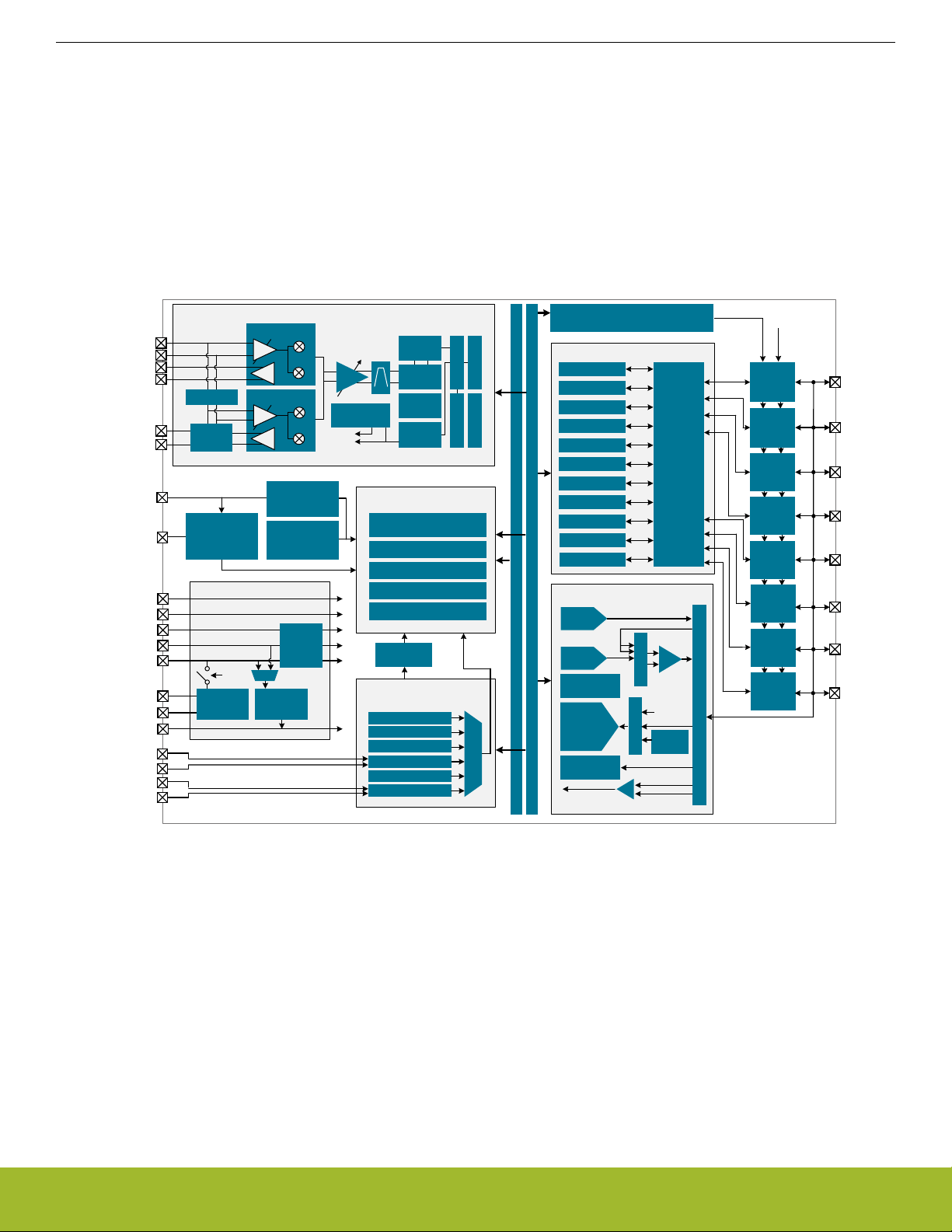
3. System Overview
3.1 Introduction
The EFR32 product family combines an energy-friendly MCU with a highly integrated radio transceiver. The devices are well suited for
any battery operated application as well as other systems requiring high performance and low energy consumption. This section gives a
short introduction to the full radio and MCU system. The detailed functional description can be found in the EFR32xG12 Wireless
Gecko Reference Manual.
A block diagram of the EFR32FG12 family is shown in Figure 3.1 Detailed EFR32FG12 Block Diagram on page 8. The diagram
shows a superset of features available on the family, which vary by OPN. For more information about specific device features, consult
Ordering Information.
SUBGRF_IP
SUBGRF_IN
SUBGRF_OP
SUBGRF_ON
2G4RF_IOP
2G4RF_ION
RESETn
Debug Signals
(shared w/GPIO)
PAVDD
RFVDD
IOVDD
AVDD
DVDD
VREGVDD
VREGSW
DECOUPLE
LFXTAL_P
LFXTAL_N
HFXTAL_P
HFXTAL_N
Sub-GHz RF
LNA
PA
RFSENSE
BALUN
Serial Wire
and ETM
Debug /
Programming
2.4 GHz RF
LNA
PA
Energy Management
bypass
DC-DC
Converter
Voltage
Regulator
Radio Transceiver
I
PGA
Q
I
Frequency
Synthesizer
To RF
Frontend
Q
Circuits
Reset
Management
Unit
Brown Out /
Power-On
Reset
Voltage
Monitor
DEMOD
IFADC
AGC
MOD
FRC
CRC
ARM Cortex-M4 Core
Up to 1024 KB ISP Flash
Program Memory
Up to 256 KB RAM
Memory Protection Unit
Floating Point Unit
LDMA Controller
Watchdog
Timer
Clock Management
ULFRCO
AUXHFRCO
LFRCO
LFXO
HFRCO
HFXO
BUFC
RAC
Port I/O Configuration
IOVDD
Digital Peripherals
LETIMER
TIMER
CRYOTIMER
PCNT
RTC / RTCC
USART
LEUART
I2C
CRYPTO
A
A
H
P
B
B
CRC
LESENSE
Port
Mapper
Analog Peripherals
IDAC
-
Mux & FB
Input Mux
+
-
+
Op-Amp
VDD
Temp
Sense
APORT
VDAC
Internal
Reference
12-bit ADC
Capacitive
Sense
Analog Comparator
Port A
Drivers
Port B
Drivers
Port C
Drivers
Port D
Drivers
Port F
Drivers
Port I
Drivers
Port J
Drivers
Port K
Drivers
PAn
PBn
PCn
PDn
PFn
PIn
PJn
PKn
Figure 3.1. Detailed EFR32FG12 Block Diagram
3.2 Radio
The Gecko family features a radio transceiver supporting proprietary wireless protocols.
3.2.1 Antenna Interface
The 2.4 GHz antenna interface consists of two pins (2G4RF_IOP and 2G4RF_ION) that interface directly to the on-chip BALUN. The
2G4RF_ION pin should be grounded externally.
The external components and power supply connections for the antenna interface typical applications are shown in the RF Matching
Networks section.
silabs.com | Building a more connected world. Rev. 1.6 | 8
Page 9

EFR32FG12 Gecko Proprietary Protocol SoC Family Data Sheet
System Overview
3.2.2 Fractional-N Frequency Synthesizer
The EFR32FG12 contains a high performance, low phase noise, fully integrated fractional-N frequency synthesizer. The synthesizer is
used in receive mode to generate the LO frequency used by the down-conversion mixer. It is also used in transmit mode to directly
generate the modulated RF carrier.
The fractional-N architecture provides excellent phase noise performance combined with frequency resolution better than 100 Hz, with
low energy consumption. The synthesizer has fast frequency settling which allows very short receiver and transmitter wake up times to
optimize system energy consumption.
3.2.3 Receiver Architecture
The EFR32FG12 uses a low-IF receiver architecture, consisting of a Low-Noise Amplifier (LNA) followed by an I/Q down-conversion
mixer, employing a crystal reference. The I/Q signals are further filtered and amplified before being sampled by the IF analog-to-digital
converter (IFADC).
The IF frequency is configurable from 150 kHz to 1371 kHz. The IF can further be configured for high-side or low-side injection, providing flexibility with respect to known interferers at the image frequency.
The Automatic Gain Control (AGC) block adjusts the receiver gain to optimize performance and avoid saturation for excellent selectivity
and blocking performance. The 2.4 GHz radio is calibrated at production to improve image rejection performance. The sub-GHz radio
can be calibrated on-demand by the user for the desired frequency band.
Demodulation is performed in the digital domain. The demodulator performs configurable decimation and channel filtering to allow receive bandwidths ranging from 0.1 to 2530 kHz. High carrier frequency and baud rate offsets are tolerated by active estimation and
compensation. Advanced features supporting high quality communication under adverse conditions include forward error correction by
block and convolutional coding as well as Direct Sequence Spread Spectrum (DSSS) for 2.4 GHz and sub-GHz bands.
A Received Signal Strength Indicator (RSSI) is available for signal quality metrics, for level-based proximity detection, and for RF channel access by Collision Avoidance (CA) or Listen Before Talk (LBT) algorithms. An RSSI capture value is associated with each received
frame and the dynamic RSSI measurement can be monitored throughout reception.
The EFR32FG12 features integrated support for antenna diversity to mitigate the problem of frequency-selective fading due to multipath
propagation and improve link budget. Support for antenna diversity is available for specific PHY configurations in 2.4 GHz and sub-GHz
bands. Internal configurable hardware controls an external switch for automatic switching between antennae during RF receive detection operations.
Note: Due to the shorter preamble of 802.15.4 and BLE packets, RX diversity is not supported.
3.2.4 Transmitter Architecture
The EFR32FG12 uses a direct-conversion transmitter architecture. For constant envelope modulation formats, the modulator controls
phase and frequency modulation in the frequency synthesizer. Transmit symbols or chips are optionally shaped by a digital shaping
filter. The shaping filter is fully configurable, including the BT product, and can be used to implement Gaussian or Raised Cosine shaping.
Carrier Sense Multiple Access - Collision Avoidance (CSMA-CA) or Listen Before Talk (LBT) algorithms can be automatically timed by
the EFR32FG12. These algorithms are typically defined by regulatory standards to improve inter-operability in a given bandwidth between devices that otherwise lack synchronized RF channel access.
3.2.5 Wake on Radio
The Wake on Radio feature allows flexible, autonomous RF sensing, qualification, and demodulation without required MCU activity, using a subsystem of the EFR32FG12 including the Radio Controller (RAC), Peripheral Reflex System (PRS), and Low Energy peripherals.
silabs.com | Building a more connected world. Rev. 1.6 | 9
Page 10

EFR32FG12 Gecko Proprietary Protocol SoC Family Data Sheet
System Overview
3.2.6 RFSENSE
The RFSENSE peripheral generates a system wakeup interrupt upon detection of wideband RF energy at the antenna interface, providing true RF wakeup capabilities from low energy modes including EM2, EM3 and EM4.
RFSENSE triggers on a relatively strong RF signal and is available in the lowest energy modes, allowing exceptionally low energy consumption. RFSENSE does not demodulate or otherwise qualify the received signal, but software may respond to the wakeup event by
enabling normal RF reception.
Various strategies for optimizing power consumption and system response time in presence of false alarms may be employed using
available timer peripherals.
3.2.7 Flexible Frame Handling
EFR32FG12 has an extensive and flexible frame handling support for easy implementation of even complex communication protocols.
The Frame Controller (FRC) supports all low level and timing critical tasks together with the Radio Controller and Modulator/Demodulator:
• Highly adjustable preamble length
• Up to 2 simultaneous synchronization words, each up to 32 bits and providing separate interrupts
• Frame disassembly and address matching (filtering) to accept or reject frames
• Automatic ACK frame assembly and transmission
• Fully flexible CRC generation and verification:
• Multiple CRC values can be embedded in a single frame
• 8, 16, 24 or 32-bit CRC value
• Configurable CRC bit and byte ordering
• Selectable bit-ordering (least significant or most significant bit first)
• Optional data whitening
• Optional Forward Error Correction (FEC), including convolutional encoding / decoding and block encoding / decoding
• Half rate convolutional encoder and decoder with constraint lengths from 2 to 7 and optional puncturing
• Optional symbol interleaving, typically used in combination with FEC
• Symbol coding, such as Manchester or DSSS, or biphase space encoding using FEC hardware
• UART encoding over air, with start and stop bit insertion / removal
• Test mode support, such as modulated or unmodulated carrier output
• Received frame timestamping
3.2.8 Packet and State Trace
The EFR32FG12 Frame Controller has a packet and state trace unit that provides valuable information during the development phase.
It features:
• Non-intrusive trace of transmit data, receive data and state information
• Data observability on a single-pin UART data output, or on a two-pin SPI data output
• Configurable data output bitrate / baudrate
• Multiplexed transmitted data, received data and state / meta information in a single serial data stream
3.2.9 Data Buffering
The EFR32FG12 features an advanced Radio Buffer Controller (BUFC) capable of handling up to 4 buffers of adjustable size from 64
bytes to 4096 bytes. Each buffer can be used for RX, TX or both. The buffer data is located in RAM, enabling zero-copy operations.
3.2.10 Radio Controller (RAC)
The Radio Controller controls the top level state of the radio subsystem in the EFR32FG12. It performs the following tasks:
• Precisely-timed control of enabling and disabling of the receiver and transmitter circuitry
• Run-time calibration of receiver, transmitter and frequency synthesizer
• Detailed frame transmission timing, including optional LBT or CSMA-CA
silabs.com | Building a more connected world. Rev. 1.6 | 10
Page 11

EFR32FG12 Gecko Proprietary Protocol SoC Family Data Sheet
System Overview
3.2.11 Random Number Generator
The Frame Controller (FRC) implements a random number generator that uses entropy gathered from noise in the RF receive chain.
The data is suitable for use in cryptographic applications.
Output from the random number generator can be used either directly or as a seed or entropy source for software-based random number generator algorithms such as Fortuna.
silabs.com | Building a more connected world. Rev. 1.6 | 11
Page 12

EFR32FG12 Gecko Proprietary Protocol SoC Family Data Sheet
System Overview
3.3 Power
The EFR32FG12 has an Energy Management Unit (EMU) and efficient integrated regulators to generate internal supply voltages. Only
a single external supply voltage is required, from which all internal voltages are created. An optional integrated DC-DC buck regulator
can be utilized to further reduce the current consumption. The DC-DC regulator requires one external inductor and one external capacitor.
The EFR32FG12 device family includes support for internal supply voltage scaling, as well as two different power domains groups for
peripherals. These enhancements allow for further supply current reductions and lower overall power consumption.
AVDD and VREGVDD need to be 1.8 V or higher for the MCU to operate across all conditions; however the rest of the system will
operate down to 1.62 V, including the digital supply and I/O. This means that the device is fully compatible with 1.8 V components.
Running from a sufficiently high supply, the device can use the DC-DC to regulate voltage not only for itself, but also for other PCB
components, supplying up to a total of 200 mA.
3.3.1 Energy Management Unit (EMU)
The Energy Management Unit manages transitions of energy modes in the device. Each energy mode defines which peripherals and
features are available and the amount of current the device consumes. The EMU can also be used to turn off the power to unused RAM
blocks, and it contains control registers for the DC-DC regulator and the Voltage Monitor (VMON). The VMON is used to monitor multiple supply voltages. It has multiple channels which can be programmed individually by the user to determine if a sensed supply has
fallen below a chosen threshold.
3.3.2 DC-DC Converter
The DC-DC buck converter covers a wide range of load currents and provides up to 90% efficiency in energy modes EM0, EM1, EM2
and EM3, and can supply up to 200 mA to the device and surrounding PCB components. Patented RF noise mitigation allows operation
of the DC-DC converter without degrading sensitivity of radio components. Protection features include programmable current limiting,
short-circuit protection, and dead-time protection. The DC-DC converter may also enter bypass mode when the input voltage is too low
for efficient operation. In bypass mode, the DC-DC input supply is internally connected directly to its output through a low resistance
switch. Bypass mode also supports in-rush current limiting to prevent input supply voltage droops due to excessive output current transients.
3.3.3 Power Domains
The EFR32FG12 has two peripheral power domains for operation in EM2 and lower. If all of the peripherals in a peripheral power domain are configured as unused, the power domain for that group will be powered off in the low-power mode, reducing the overall current consumption of the device.
Table 3.1. Peripheral Power Subdomains
Peripheral Power Domain 1 Peripheral Power Domain 2
ACMP0 ACMP1
PCNT0 PCNT1
ADC0 PCNT2
LETIMER0 CSEN
LESENSE DAC0
APORT LEUART0
- I2C0
- I2C1
- IDAC
silabs.com | Building a more connected world. Rev. 1.6 | 12
Page 13

EFR32FG12 Gecko Proprietary Protocol SoC Family Data Sheet
System Overview
3.4 General Purpose Input/Output (GPIO)
EFR32FG12 has up to 65 General Purpose Input/Output pins. Each GPIO pin can be individually configured as either an output or input. More advanced configurations including open-drain, open-source, and glitch-filtering can be configured for each individual GPIO
pin. The GPIO pins can be overridden by peripheral connections, like SPI communication. Each peripheral connection can be routed to
several GPIO pins on the device. The input value of a GPIO pin can be routed through the Peripheral Reflex System to other peripherals. The GPIO subsystem supports asynchronous external pin interrupts.
3.5 Clocking
3.5.1 Clock Management Unit (CMU)
The Clock Management Unit controls oscillators and clocks in the EFR32FG12. Individual enabling and disabling of clocks to all peripherals is performed by the CMU. The CMU also controls enabling and configuration of the oscillators. A high degree of flexibility allows
software to optimize energy consumption in any specific application by minimizing power dissipation in unused peripherals and oscillators.
3.5.2 Internal and External Oscillators
The EFR32FG12 supports two crystal oscillators and fully integrates four RC oscillators, listed below.
• A high frequency crystal oscillator (HFXO) with integrated load capacitors, tunable in small steps, provides a precise timing reference for the MCU. Crystal frequencies in the range from 38 to 40 MHz are supported. An external clock source such as a TCXO can
also be applied to the HFXO input for improved accuracy over temperature.
• A 32.768 kHz crystal oscillator (LFXO) provides an accurate timing reference for low energy modes.
• An integrated high frequency RC oscillator (HFRCO) is available for the MCU system, when crystal accuracy is not required. The
HFRCO employs fast startup at minimal energy consumption combined with a wide frequency range.
• An integrated auxilliary high frequency RC oscillator (AUXHFRCO) is available for timing the general-purpose ADC and the Serial
Wire Viewer port with a wide frequency range.
• An integrated low frequency 32.768 kHz RC oscillator (LFRCO) can be used as a timing reference in low energy modes, when crystal accuracy is not required.
• An integrated ultra-low frequency 1 kHz RC oscillator (ULFRCO) is available to provide a timing reference at the lowest energy consumption in low energy modes.
3.6 Counters/Timers and PWM
3.6.1 Timer/Counter (TIMER)
TIMER peripherals keep track of timing, count events, generate PWM outputs and trigger timed actions in other peripherals through the
PRS system. The core of each TIMER is a 16-bit counter with up to 4 compare/capture channels. Each channel is configurable in one
of three modes. In capture mode, the counter state is stored in a buffer at a selected input event. In compare mode, the channel output
reflects the comparison of the counter to a programmed threshold value. In PWM mode, the TIMER supports generation of pulse-width
modulation (PWM) outputs of arbitrary waveforms defined by the sequence of values written to the compare registers, with optional
dead-time insertion available in timer unit TIMER_0 only.
3.6.2 Wide Timer/Counter (WTIMER)
WTIMER peripherals function just as TIMER peripherals, but are 32 bits wide. They keep track of timing, count events, generate PWM
outputs and trigger timed actions in other peripherals through the PRS system. The core of each WTIMER is a 32-bit counter with up to
4 compare/capture channels. Each channel is configurable in one of three modes. In capture mode, the counter state is stored in a
buffer at a selected input event. In compare mode, the channel output reflects the comparison of the counter to a programmed threshold value. In PWM mode, the WTIMER supports generation of pulse-width modulation (PWM) outputs of arbitrary waveforms defined by
the sequence of values written to the compare registers, with optional dead-time insertion available in timer unit WTIMER_0 only.
3.6.3 Real Time Counter and Calendar (RTCC)
The Real Time Counter and Calendar (RTCC) is a 32-bit counter providing timekeeping in all energy modes. The RTCC includes a
Binary Coded Decimal (BCD) calendar mode for easy time and date keeping. The RTCC can be clocked by any of the on-board oscillators with the exception of the AUXHFRCO, and it is capable of providing system wake-up at user defined instances. When receiving
frames, the RTCC value can be used for timestamping. The RTCC includes 128 bytes of general purpose data retention, allowing easy
and convenient data storage in all energy modes down to EM4H.
silabs.com | Building a more connected world. Rev. 1.6 | 13
Page 14

EFR32FG12 Gecko Proprietary Protocol SoC Family Data Sheet
System Overview
3.6.4 Low Energy Timer (LETIMER)
The unique LETIMER is a 16-bit timer that is available in energy mode EM0 Active, EM1 Sleep, EM2 Deep Sleep, and EM3 Stop. This
allows it to be used for timing and output generation when most of the device is powered down, allowing simple tasks to be performed
while the power consumption of the system is kept at an absolute minimum. The LETIMER can be used to output a variety of waveforms with minimal software intervention. The LETIMER is connected to the Real Time Counter and Calendar (RTCC), and can be configured to start counting on compare matches from the RTCC.
3.6.5 Ultra Low Power Wake-up Timer (CRYOTIMER)
The CRYOTIMER is a 32-bit counter that is capable of running in all energy modes. It can be clocked by either the 32.768 kHz crystal
oscillator (LFXO), the 32.768 kHz RC oscillator (LFRCO), or the 1 kHz RC oscillator (ULFRCO). It can provide periodic Wakeup events
and PRS signals which can be used to wake up peripherals from any energy mode. The CRYOTIMER provides a wide range of interrupt periods, facilitating flexible ultra-low energy operation.
3.6.6 Pulse Counter (PCNT)
The Pulse Counter (PCNT) peripheral can be used for counting pulses on a single input or to decode quadrature encoded inputs. The
clock for PCNT is selectable from either an external source on pin PCTNn_S0IN or from an internal timing reference, selectable from
among any of the internal oscillators, except the AUXHFRCO. The peripheral may operate in energy mode EM0 Active, EM1 Sleep,
EM2 Deep Sleep, and EM3 Stop.
3.6.7 Watchdog Timer (WDOG)
The watchdog timer can act both as an independent watchdog or as a watchdog synchronous with the CPU clock. It has windowed
monitoring capabilities, and can generate a reset or different interrupts depending on the failure mode of the system. The watchdog can
also monitor autonomous systems driven by PRS.
3.7 Communications and Other Digital Peripherals
3.7.1 Universal Synchronous/Asynchronous Receiver/Transmitter (USART)
The Universal Synchronous/Asynchronous Receiver/Transmitter is a flexible serial I/O interface. It supports full duplex asynchronous
UART communication with hardware flow control as well as RS-485, SPI, MicroWire and 3-wire. It can also interface with devices supporting:
• ISO7816 SmartCards
• IrDA
•
I2S
3.7.2 Low Energy Universal Asynchronous Receiver/Transmitter (LEUART)
The unique LEUARTTM provides two-way UART communication on a strict power budget. Only a 32.768 kHz clock is needed to allow
UART communication up to 9600 baud. The LEUART includes all necessary hardware to make asynchronous serial communication
possible with a minimum of software intervention and energy consumption.
3.7.3 Inter-Integrated Circuit Interface (I2C)
The I2C interface enables communication between the MCU and a serial I2C bus. It is capable of acting as both a master and a slave
and supports multi-master buses. Standard-mode, fast-mode and fast-mode plus speeds are supported, allowing transmission rates
from 10 kbit/s up to 1 Mbit/s. Slave arbitration and timeouts are also available, allowing implementation of an SMBus-compliant system.
The interface provided to software by the I2C peripheral allows precise timing control of the transmission process and highly automated
transfers. Automatic recognition of slave addresses is provided in active and low energy modes.
3.7.4 Peripheral Reflex System (PRS)
The Peripheral Reflex System provides a communication network between different peripherals without software involvement. Peripherals producing Reflex signals are called producers. The PRS routes Reflex signals from producers to consumer peripherals, which in
turn perform actions in response. Edge triggers and other functionality such as simple logic operations (AND, OR, NOT) can be applied
by the PRS to the signals. The PRS allows peripheral to act autonomously without waking the MCU core, saving power.
silabs.com | Building a more connected world. Rev. 1.6 | 14
Page 15

EFR32FG12 Gecko Proprietary Protocol SoC Family Data Sheet
System Overview
3.7.5 Low Energy Sensor Interface (LESENSE)
The Low Energy Sensor Interface LESENSETM is a highly configurable sensor interface with support for up to 16 individually configurable sensors. By controlling the analog comparators, ADC, and DAC, LESENSE is capable of supporting a wide range of sensors and
measurement schemes, and can for instance measure LC sensors, resistive sensors and capacitive sensors. LESENSE also includes a
programmable finite state machine which enables simple processing of measurement results without CPU intervention. LESENSE is
available in energy mode EM2, in addition to EM0 and EM1, making it ideal for sensor monitoring in applications with a strict energy
budget.
3.8 Security Features
3.8.1 General Purpose Cyclic Redundancy Check (GPCRC)
The GPCRC block implements a Cyclic Redundancy Check (CRC) function. It supports both 32-bit and 16-bit polynomials. The supported 32-bit polynomial is 0x04C11DB7 (IEEE 802.3), while the 16-bit polynomial can be programmed to any value, depending on the
needs of the application.
3.8.2 Crypto Accelerator (CRYPTO)
The Crypto Accelerator is a fast and energy-efficient autonomous hardware encryption and decryption accelerator. EFR32 devices support AES encryption and decryption with 128- or 256-bit keys, ECC over both GF(P) and GF(2m), SHA-1 and SHA-2 (SHA-224 and
SHA-256).
Supported block cipher modes of operation for AES include: ECB, CTR, CBC, PCBC, CFB, OFB, GCM, CBC-MAC, GMAC and CCM.
Supported ECC NIST recommended curves include P-192, P-224, P-256, K-163, K-233, B-163 and B-233.
The CRYPTO1 block is tightly linked to the Radio Buffer Controller (BUFC) enabling fast and efficient autonomous cipher operations on
data buffer content. It allows fast processing of GCM (AES), ECC and SHA with little CPU intervention.
CRYPTO also provides trigger signals for DMA read and write operations.
3.8.3 True Random Number Generator (TRNG)
The TRNG is a non-deterministic random number generator based on a full hardware solution. The TRNG is validated with NIST800-22
and AIS-31 test suites as well as being suitable for FIPS 140-2 certification (for the purposes of cryptographic key generation).
Note: TRNG operation is only supported at VSCALE2. TRNG cannot be used at VSCALE0.
3.8.4 Security Management Unit (SMU)
The Security Management Unit (SMU) allows software to set up fine-grained security for peripheral access, which is not possible in the
Memory Protection Unit (MPU). Peripherals may be secured by hardware on an individual basis, such that only priveleged accesses to
the peripheral's register interface will be allowed. When an access fault occurs, the SMU reports the specific peripheral involved and
can optionally generate an interrupt.
3.9 Analog
3.9.1 Analog Port (APORT)
The Analog Port (APORT) is an analog interconnect matrix allowing access to many analog peripherals on a flexible selection of pins.
Each APORT bus consists of analog switches connected to a common wire. Since many clients can operate differentially, buses are
grouped by X/Y pairs.
3.9.2 Analog Comparator (ACMP)
The Analog Comparator is used to compare the voltage of two analog inputs, with a digital output indicating which input voltage is higher. Inputs are selected from among internal references and external pins. The tradeoff between response time and current consumption
is configurable by software. Two 6-bit reference dividers allow for a wide range of internally-programmable reference sources. The
ACMP can also be used to monitor the supply voltage. An interrupt can be generated when the supply falls below or rises above the
programmable threshold.
silabs.com | Building a more connected world. Rev. 1.6 | 15
Page 16

EFR32FG12 Gecko Proprietary Protocol SoC Family Data Sheet
System Overview
3.9.3 Analog to Digital Converter (ADC)
The ADC is a Successive Approximation Register (SAR) architecture, with a resolution of up to 12 bits at up to 1 Msps. The output
sample resolution is configurable and additional resolution is possible using integrated hardware for averaging over multiple samples.
The ADC includes integrated voltage references and an integrated temperature sensor. Inputs are selectable from a wide range of
sources, including pins configurable as either single-ended or differential.
3.9.4 Capacitive Sense (CSEN)
The CSEN peripheral is a dedicated Capacitive Sensing block for implementing touch-sensitive user interface elements such a
switches and sliders. The CSEN peripheral uses a charge ramping measurement technique, which provides robust sensing even in
adverse conditions including radiated noise and moisture. The peripheral can be configured to take measurements on a single port pin
or scan through multiple pins and store results to memory through DMA. Several channels can also be shorted together to measure the
combined capacitance or implement wake-on-touch from very low energy modes. Hardware includes a digital accumulator and an averaging filter, as well as digital threshold comparators to reduce software overhead.
3.9.5 Digital to Analog Current Converter (IDAC)
The IDAC can source or sink a configurable constant current. This current can be driven on an output pin or routed to the selected ADC
input pin for capacitive sensing. The full-scale current is programmable between 0.05 µA and 64 µA with several ranges consisting of
various step sizes.
3.9.6 Digital to Analog Converter (VDAC)
The Digital to Analog Converter (VDAC) can convert a digital value to an analog output voltage. The VDAC is a fully differential, 500
ksps, 12-bit converter. The opamps are used in conjunction with the VDAC, to provide output buffering. One opamp is used per singleended channel, or two opamps are used to provide differential outputs. The VDAC may be used for a number of different applications
such as sensor interfaces or sound output. The VDAC can generate high-resolution analog signals while the MCU is operating at low
frequencies and with low total power consumption. Using DMA and a timer, the VDAC can be used to generate waveforms without any
CPU intervention. The VDAC is available in all energy modes down to and including EM3.
3.9.7 Operational Amplifiers
The opamps are low power amplifiers with a high degree of flexibility targeting a wide variety of standard opamp application areas, and
are available down to EM3. With flexible built-in programming for gain and interconnection they can be configured to support multiple
common opamp functions. All pins are also available externally for filter configurations. Each opamp has a rail to rail input and a rail to
rail output. They can be used in conjunction with the VDAC peripheral or in stand-alone configurations. The opamps save energy, PCB
space, and cost as compared with standalone opamps because they are integrated on-chip.
3.10 Reset Management Unit (RMU)
The RMU is responsible for handling reset of the EFR32FG12. A wide range of reset sources are available, including several power
supply monitors, pin reset, software controlled reset, core lockup reset, and watchdog reset.
3.11 Core and Memory
3.11.1 Processor Core
The ARM Cortex-M processor includes a 32-bit RISC processor integrating the following features and tasks in the system:
• ARM Cortex-M4 RISC processor achieving 1.25 Dhrystone MIPS/MHz
• Memory Protection Unit (MPU) supporting up to 8 memory segments
• Up to 1024 kB flash program memory
• Up to 256 kB RAM data memory
• Configuration and event handling of all peripherals
• 2-pin Serial-Wire debug interface
silabs.com | Building a more connected world. Rev. 1.6 | 16
Page 17

EFR32FG12 Gecko Proprietary Protocol SoC Family Data Sheet
System Overview
3.11.2 Memory System Controller (MSC)
The Memory System Controller (MSC) is the program memory unit of the microcontroller. The flash memory is readable and writable
from both the Cortex-M and DMA. The flash memory is divided into two blocks; the main block and the information block. Program code
is normally written to the main block, whereas the information block is available for special user data and flash lock bits. There is also a
read-only page in the information block containing system and device calibration data. Read and write operations are supported in energy modes EM0 Active and EM1 Sleep.
3.11.3 Linked Direct Memory Access Controller (LDMA)
The Linked Direct Memory Access (LDMA) controller allows the system to perform memory operations independently of software. This
reduces both energy consumption and software workload. The LDMA allows operations to be linked together and staged, enabling sophisticated operations to be implemented.
silabs.com | Building a more connected world. Rev. 1.6 | 17
Page 18
EFR32FG12 Gecko Proprietary Protocol SoC Family Data Sheet
System Overview
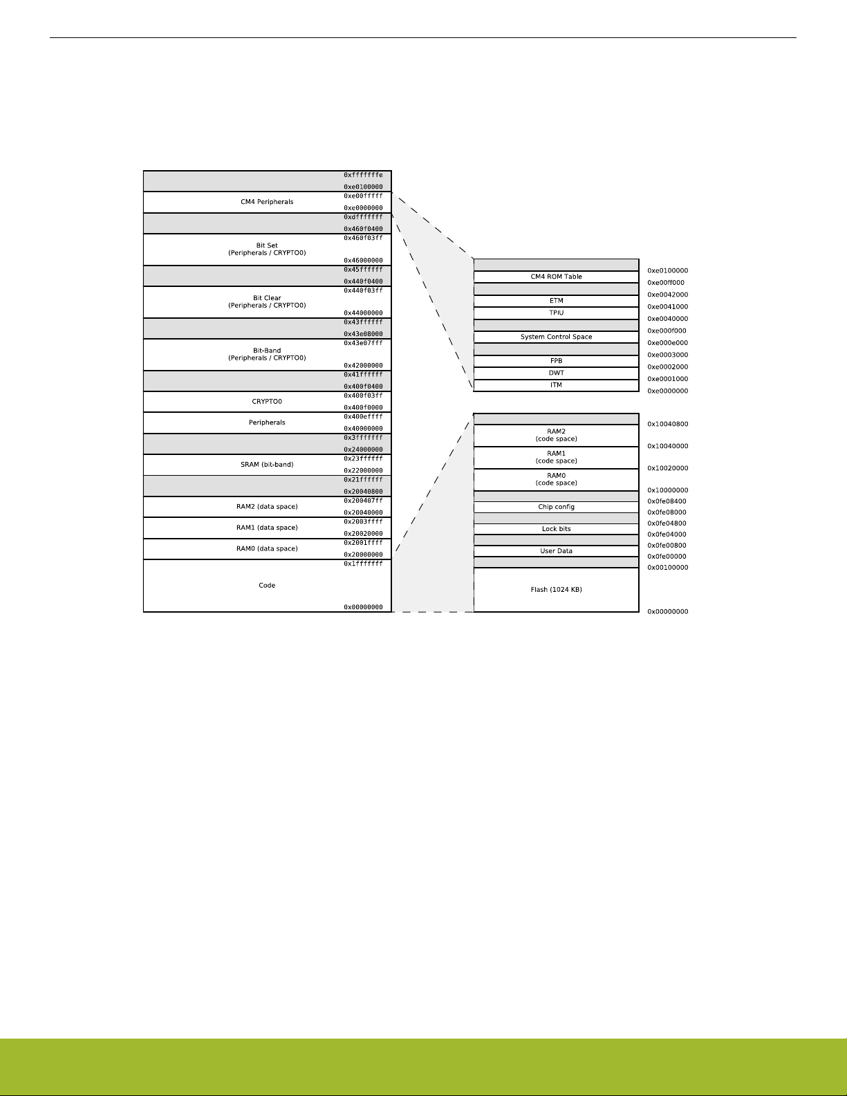
3.12 Memory Map
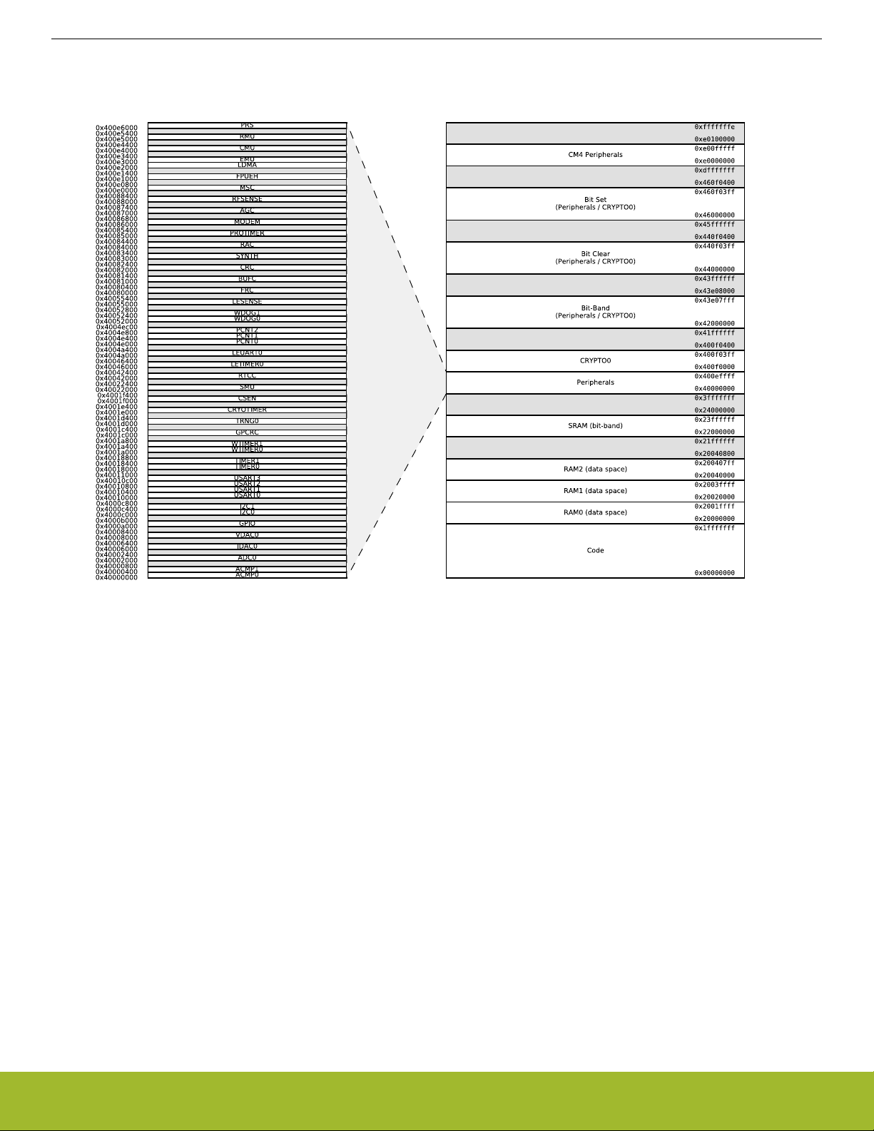
The EFR32FG12 memory map is shown in the figures below. RAM and flash sizes are for the largest memory configuration.
Figure 3.2. EFR32FG12 Memory Map — Core Peripherals and Code Space
silabs.com | Building a more connected world. Rev. 1.6 | 18
Page 19
EFR32FG12 Gecko Proprietary Protocol SoC Family Data Sheet
System Overview
Figure 3.3. EFR32FG12 Memory Map — Peripherals
silabs.com | Building a more connected world. Rev. 1.6 | 19
Page 20

EFR32FG12 Gecko Proprietary Protocol SoC Family Data Sheet
System Overview
3.13 Configuration Summary
The features of the EFR32FG12 are a subset of the feature set described in the device reference manual. The table below describes
device specific implementation of the features. Remaining modules support full configuration.
Table 3.2. Configuration Summary
Module Configuration Pin Connections
USART0 IrDA
US0_TX, US0_RX, US0_CLK, US0_CS
SmartCard
USART1
I2S
US1_TX, US1_RX, US1_CLK, US1_CS
SmartCard
USART2 IrDA
US2_TX, US2_RX, US2_CLK, US2_CS
SmartCard
USART3
I2S
US3_TX, US3_RX, US3_CLK, US3_CS
SmartCard
TIMER0 with DTI TIM0_CC[2:0], TIM0_CDTI[2:0]
TIMER1 - TIM1_CC[3:0]
WTIMER0 with DTI WTIM0_CC[2:0], WTIM0_CDTI[2:0]
WTIMER1 - WTIM1_CC[3:0]
silabs.com | Building a more connected world. Rev. 1.6 | 20
Page 21

EFR32FG12 Gecko Proprietary Protocol SoC Family Data Sheet
Electrical Specifications
4. Electrical Specifications
4.1 Electrical Characteristics
All electrical parameters in all tables are specified under the following conditions, unless stated otherwise:
• Typical values are based on T
• Radio performance numbers are measured in conducted mode, based on Silicon Laboratories reference designs using output power-specific external RF impedance-matching networks for interfacing to a 50 Ω antenna.
• Minimum and maximum values represent the worst conditions across supply voltage, process variation, and operating temperature,
unless stated otherwise.
Refer to 4.1.2.1 General Operating Conditions for more details about operational supply and temperature limits.
=25 °C and VDD= 3.3 V, by production test and/or technology characterization.
AMB
silabs.com | Building a more connected world. Rev. 1.6 | 21
Page 22

EFR32FG12 Gecko Proprietary Protocol SoC Family Data Sheet
Electrical Specifications
4.1.1 Absolute Maximum Ratings
Stresses above those listed below may cause permanent damage to the device. This is a stress rating only and functional operation of
the devices at those or any other conditions above those indicated in the operation listings of this specification is not implied. Exposure
to maximum rating conditions for extended periods may affect device reliability. For more information on the available quality and reliability data, see the Quality and Reliability Monitor Report at http://www.silabs.com/support/quality/pages/default.aspx.
Table 4.1. Absolute Maximum Ratings
Parameter Symbol Test Condition Min Typ Max Unit
Storage temperature range T
Voltage on any supply pin V
Voltage ramp rate on any
supply pin
DC voltage on any GPIO pin V
Voltage on HFXO pins V
Input RF level on pins
2G4RF_IOP and
2G4RF_ION
Voltage differential between
RF pins (2G4RF_IOP 2G4RF_ION)
Absolute voltage on RF pins
2G4RF_IOP and
2G4RF_ION
Absolute voltage on SubGHz RF pins
STG
DDMAX
V
DDRAMPMAX
DIGPIN
HFXOPIN
P
RFMAX2G4
V
MAXDIFF2G4
V
MAX2G4
V
MAXSUBG
-50 — 150 °C
-0.3 — 3.8 V
— — 1 V / µs
5V tolerant GPIO pins1 2
3
-0.3 — Min of 5.25
and IOVDD
+2
Standard GPIO pins -0.3 — IOVDD+0.3 V
-0.3 — 1.4 V
— — 10 dBm
-50 — 50 mV
-0.3 — 3.8 V
Pins SUBGRF_OP and
-0.3 — 3.8 V
SUBGRF_ON
V
Total current into VDD power
lines
Total current into VSS
ground lines
Current per I/O pin I
Current for all I/O pins I
Junction temperature T
I
VDDMAX
I
VSSMAX
IOMAX
IOALLMAX
J
Pins SUBGRF_IP and
-0.3 — 0.3 V
SUBGRF_IN,
Source — — 200 mA
Sink — — 200 mA
Sink — — 50 mA
Source — — 50 mA
Sink — — 200 mA
Source — — 200 mA
-G grade devices -40 — 105 °C
-I grade devices -40 — 125 °C
silabs.com | Building a more connected world. Rev. 1.6 | 22
Page 23

EFR32FG12 Gecko Proprietary Protocol SoC Family Data Sheet
Electrical Specifications
Parameter Symbol Test Condition Min Typ Max Unit
Note:
1. When a GPIO pin is routed to the analog block through the APORT, the maximum voltage = IOVDD.
2. Valid for IOVDD in valid operating range or when IOVDD is undriven (high-Z). If IOVDD is connected to a low-impedance source
below the valid operating range (e.g. IOVDD shorted to VSS), the pin voltage maximum is IOVDD + 0.3 V, to avoid exceeding the
maximum IO current specifications.
3. To operate above the IOVDD supply rail, over-voltage tolerance must be enabled according to the GPIO_Px_OVTDIS register.
Pins with over-voltage tolerance disabled have the same limits as Standard GPIO.
silabs.com | Building a more connected world. Rev. 1.6 | 23
Page 24

EFR32FG12 Gecko Proprietary Protocol SoC Family Data Sheet
4.1.2 Operating Conditions
When assigning supply sources, the following requirements must be observed:
• VREGVDD must be greater than or equal to AVDD, DVDD, RFVDD, PAVDD and all IOVDD supplies.
• VREGVDD = AVDD
• DVDD ≤ AVDD
• IOVDD ≤ AVDD
• RFVDD ≤ AVDD
• PAVDD ≤ AVDD
Electrical Specifications
silabs.com | Building a more connected world. Rev. 1.6 | 24
Page 25
EFR32FG12 Gecko Proprietary Protocol SoC Family Data Sheet
Electrical Specifications
4.1.2.1 General Operating Conditions
Table 4.2. General Operating Conditions
Parameter Symbol Test Condition Min Typ Max Unit
Operating ambient temperature range
AVDD supply voltage
1
2
VREGVDD operating supply
voltage2
3
VREGVDD current I
RFVDD operating supply
voltage
DVDD operating supply voltage
PAVDD operating supply
voltage
IOVDD operating supply voltage
DECOUPLE output capaci-
6
tor5
T
A
V
AVDD
V
VREGVDD
VREGVDD
V
RFVDD
V
DVDD
V
PAVDD
V
IOVDD
C
DECOUPLE
-G temperature grade -40 25 85 °C
-I temperature grade -40 25 125 °C
1.8 3.3 3.8 V
DCDC in regulation 2.4 3.3 3.8 V
DCDC in bypass, 50mA load 1.8 3.3 3.8 V
DCDC not in use. DVDD external-
1.8 3.3 3.8 V
ly shorted to VREGVDD
DCDC in bypass, T ≤ 85 °C — — 200 mA
DCDC in bypass, T > 85 °C — — 100 mA
All IOVDD pins
1.62 — V
1.62 — V
1.62 — V
4
1.62 — V
VREGVDD
VREGVDD
VREGVDD
VREGVDD
V
V
V
V
0.75 1.0 2.75 µF
Difference between AVDD
and VREGVDD, ABS(AVDD-
VREGVDD)
2
HFCORECLK frequency f
HFCLK frequency f
dV
DD
CORE
HFCLK
— — 0.1 V
VSCALE2, MODE = WS1 — — 40 MHz
VSCALE2, MODE = WS0 — — 25 MHz
VSCALE0, MODE = WS2 — — 20 MHz
VSCALE0, MODE = WS1 — — 14 MHz
VSCALE0, MODE = WS0 — — 7 MHz
VSCALE2 — — 40 MHz
VSCALE0 — — 20 MHz
silabs.com | Building a more connected world. Rev. 1.6 | 25
Page 26
EFR32FG12 Gecko Proprietary Protocol SoC Family Data Sheet
Electrical Specifications
Parameter Symbol Test Condition Min Typ Max Unit
Note:
1. The maximum limit on TA may be lower due to device self-heating, which depends on the power dissipation of the specific application. TA (max) = TJ (max) - (THETAJA x PowerDissipation). Refer to the Absolute Maximum Ratings table and the Thermal
Characteristics table for TJ and THETAJA.
2. VREGVDD must be tied to AVDD. Both VREGVDD and AVDD minimum voltages must be satisfied for the part to operate.
3. The minimum voltage required in bypass mode is calculated using R
other loads can be calculated as V
DVDD_min+ILOAD
* R
BYP_max
.
4. When the CSEN peripheral is used with chopping enabled (CSEN_CTRL_CHOPEN = ENABLE), IOVDD must be equal to AVDD.
5. The system designer should consult the characteristic specs of the capacitor used on DECOUPLE to ensure its capacitance value stays within the specified bounds across temperature and DC bias.
6. VSCALE0 to VSCALE2 voltage change transitions occur at a rate of 10 mV / usec for approximately 20 usec. During this transition, peak currents will be dependent on the value of the DECOUPLE output capacitor, from 35 mA (with a 1 µF capacitor) to 70
mA (with a 2.7 µF capacitor).
4.1.3 Thermal Characteristics
from the DCDC specification table. Requirements for
BYP
Table 4.3. Thermal Characteristics
Parameter Symbol Test Condition Min Typ Max Unit
Thermal resistance, QFN48
Package
THETA
JA_QFN48
2-Layer PCB, Air velocity = 0 m/s — 75.7 — °C/W
2-Layer PCB, Air velocity = 1 m/s — 61.5 — °C/W
2-Layer PCB, Air velocity = 2 m/s — 55.4 — °C/W
4-Layer PCB, Air velocity = 0 m/s — 30.2 — °C/W
4-Layer PCB, Air velocity = 1 m/s — 26.3 — °C/W
4-Layer PCB, Air velocity = 2 m/s — 24.9 — °C/W
Thermal resistance, BGA125
Package
THETA
JA_BGA125
2-Layer PCB, Air velocity = 0 m/s — 90.7 — °C/W
2-Layer PCB, Air velocity = 1 m/s — 73.7 — °C/W
2-Layer PCB, Air velocity = 2 m/s — 66.4 — °C/W
4-Layer PCB, Air velocity = 0 m/s — 45 — °C/W
4-Layer PCB, Air velocity = 1 m/s — 39.6 — °C/W
4-Layer PCB, Air velocity = 2 m/s — 37.6 — °C/W
Thermal resistance, QFN68
Package
THETA
JA_QFN68
4-Layer PCB, Air velocity = 0 m/s — 21.5 — °C/W
4-Layer PCB, Air velocity = 1 m/s — 18.9 — °C/W
4-Layer PCB, Air velocity = 2 m/s — 17.1 — °C/W
silabs.com | Building a more connected world. Rev. 1.6 | 26
Page 27

EFR32FG12 Gecko Proprietary Protocol SoC Family Data Sheet
Electrical Specifications
4.1.4 DC-DC Converter
Test conditions: L_DCDC=4.7 µH (Murata LQH3NPN4R7MM0L), C_DCDC=4.7 µF (Samsung CL10B475KQ8NQNC), V_DCDC_I=3.3
V, V_DCDC_O=1.8 V, I_DCDC_LOAD=50 mA, Heavy Drive configuration, F_DCDC_LN=7 MHz, unless otherwise indicated.
Table 4.4. DC-DC Converter
Parameter Symbol Test Condition Min Typ Max Unit
Input voltage range V
Output voltage programmable range
1
DCDC_I
V
DCDC_O
Regulation DC accuracy ACC
Regulation window
2
Steady-state output ripple V
Output voltage under/over-
WIN
R
V
OV
shoot
DC
REG
Bypass mode, I
DCDC_LOAD
mA
Low noise (LN) mode, 1.8 V output, I
DCDC_LOAD
= 100 mA, or
= 50
1.8 — V
2.4 — V
VREGVDD_
MAX
VREGVDD_
MAX
V
V
Low power (LP) mode, 1.8 V output, I
DCDC_LOAD
Low noise (LN) mode, 1.8 V output, I
DCDC_LOAD
Low Noise (LN) mode, 1.8 V tar-
= 10 mA
= 200 mA
2.6 — V
1.8 — V
VREGVDD_
MAX
VREGVDD
1.7 — 1.9 V
V
V
get output
Low Power (LP) mode,
1.63 — 2.2 V
LPCMPBIASEMxx3 = 0, 1.8 V target output, I
DCDC_LOAD
Low Power (LP) mode,
≤ 75 µA
1.63 — 2.1 V
LPCMPBIASEMxx3 = 3, 1.8 V target output, I
DCDC_LOAD
≤ 10 mA
Radio disabled — 3 — mVpp
CCM Mode (LNFORCECCM3 =
— 25 60 mV
1), Load changes between 0 mA
and 100 mA
DC line regulation V
DC load regulation I
REG
REG
DCM Mode (LNFORCECCM3 =
0), Load changes between 0 mA
and 10 mA
Overshoot during LP to LN
CCM/DCM mode transitions compared to DC level in LN mode
Undershoot during BYP/LP to LN
CCM (LNFORCECCM3 = 1) mode
transitions compared to DC level
in LN mode
Undershoot during BYP/LP to LN
DCM (LNFORCECCM3 = 0) mode
transitions compared to DC level
in LN mode
Input changes between
V
VREGVDD_MAX
and 2.4 V
Load changes between 0 mA and
100 mA in CCM mode
— 45 90 mV
— 200 — mV
— 40 — mV
— 100 — mV
— 0.1 — %
— 0.1 — %
silabs.com | Building a more connected world. Rev. 1.6 | 27
Page 28
EFR32FG12 Gecko Proprietary Protocol SoC Family Data Sheet
Electrical Specifications
Parameter Symbol Test Condition Min Typ Max Unit
Max load current I
LOAD_MAX
Low noise (LN) mode, Heavy
— — 200 mA
Drive4, T ≤ 85 °C
Low noise (LN) mode, Heavy
— — 100 mA
Drive4, T > 85 °C
Low noise (LN) mode, Medium
4
Drive
Low noise (LN) mode, Light
4
Drive
Low power (LP) mode,
— — 100 mA
— — 50 mA
— — 75 µA
LPCMPBIASEMxx3 = 0
Low power (LP) mode,
— — 10 mA
LPCMPBIASEMxx3 = 3
DCDC nominal output ca-
5
pacitor
DCDC nominal output induc-
C
DCDC
L
DCDC
25% tolerance 1 4.7 4.7 µF
20% tolerance 4.7 4.7 4.7 µH
tor
Resistance in Bypass mode R
BYP
— 1.2 2.5 Ω
Note:
1. Due to internal dropout, the DC-DC output will never be able to reach its input voltage, V
VREGVDD
.
2. LP mode controller is a hysteretic controller that maintains the output voltage within the specified limits.
3. LPCMPBIASEMxx refers to either LPCMPBIASEM234H in the EMU_DCDCMISCCTRL register or LPCMPBIASEM01 in the
EMU_DCDCLOEM01CFG register, depending on the energy mode.
4. Drive levels are defined by configuration of the PFETCNT and NFETCNT registers. Light Drive: PFETCNT=NFETCNT=3; Medium Drive: PFETCNT=NFETCNT=7; Heavy Drive: PFETCNT=NFETCNT=15.
5. Output voltage under/over-shoot and regulation are specified with C
must be used if C
is lower than 4.7 µF. See Application Note AN0948 for details.
DCDC
4.7 µF. Different settings for DCDCLNCOMPCTRL
DCDC
silabs.com | Building a more connected world. Rev. 1.6 | 28
Page 29
EFR32FG12 Gecko Proprietary Protocol SoC Family Data Sheet
Electrical Specifications
4.1.5 Current Consumption
4.1.5.1 Current Consumption 3.3 V without DC-DC Converter
Unless otherwise indicated, typical conditions are: VREGVDD = AVDD = DVDD = RFVDD = PAVDD = 3.3 V. T = 25 °C. DCDC is off.
Minimum and maximum values in this table represent the worst conditions across process variation at T = 25 °C.
Table 4.5. Current Consumption 3.3 V without DC-DC Converter
Parameter Symbol Test Condition Min Typ Max Unit
Current consumption in EM0
mode with all peripherals disabled
Current consumption in EM0
mode with all peripherals disabled and voltage scaling
enabled
Current consumption in EM1
mode with all peripherals disabled
I
ACTIVE
I
ACTIVE_VS
I
EM1
38.4 MHz crystal, CPU running
while loop from flash
1
38 MHz HFRCO, CPU running
— 130 — µA/MHz
— 99 — µA/MHz
Prime from flash
38 MHz HFRCO, CPU running
— 99 105 µA/MHz
while loop from flash
38 MHz HFRCO, CPU running
— 124 — µA/MHz
CoreMark from flash
26 MHz HFRCO, CPU running
— 102 108 µA/MHz
while loop from flash
1 MHz HFRCO, CPU running
— 280 435 µA/MHz
while loop from flash
19 MHz HFRCO, CPU running
— 88 — µA/MHz
while loop from flash
1 MHz HFRCO, CPU running
— 234 — µA/MHz
while loop from flash
38.4 MHz crystal
1
— 80 — µA/MHz
38 MHz HFRCO — 50 54 µA/MHz
26 MHz HFRCO — 52 58 µA/MHz
Current consumption in EM1
mode with all peripherals disabled and voltage scaling
enabled
Current consumption in EM2
mode, with voltage scaling
enabled
Current consumption in EM3
mode, with voltage scaling
enabled
Current consumption in
EM4H mode, with voltage
scaling enabled
I
EM1_VS
I
EM2_VS
I
EM3_VS
I
EM4H_VS
1 MHz HFRCO — 230 400 µA/MHz
19 MHz HFRCO — 47 — µA/MHz
1 MHz HFRCO — 193 — µA/MHz
Full 256 kB RAM retention and
— 2.9 — µA
RTCC running from LFXO
Full 256 kB RAM retention and
— 3.2 — µA
RTCC running from LFRCO
16 kB (1 bank) RAM retention and
RTCC running from LFRCO
2
Full 256 kB RAM retention and
— 2.1 3.5 µA
— 2.56 4.8 µA
CRYOTIMER running from ULFRCO
128 byte RAM retention, RTCC
— 1.0 — µA
running from LFXO
128 byte RAM retention, CRYO-
— 0.45 — µA
TIMER running from ULFRCO
128 byte RAM retention, no RTCC — 0.43 0.9 µA
silabs.com | Building a more connected world. Rev. 1.6 | 29
Page 30

EFR32FG12 Gecko Proprietary Protocol SoC Family Data Sheet
Electrical Specifications
Parameter Symbol Test Condition Min Typ Max Unit
Current consumption in
I
EM4S
No RAM retention, no RTCC — 0.04 0.1 µA
EM4S mode
Note:
1. CMU_HFXOCTRL_LOWPOWER=0.
2. CMU_LFRCOCTRL_ENVREF = 1, CMU_LFRCOCTRL_VREFUPDATE = 1
silabs.com | Building a more connected world. Rev. 1.6 | 30
Page 31

EFR32FG12 Gecko Proprietary Protocol SoC Family Data Sheet
Electrical Specifications
4.1.5.2 Current Consumption 3.3 V using DC-DC Converter
Unless otherwise indicated, typical conditions are: VREGVDD = AVDD = IOVDD = 3.3 V, DVDD = RFVDD = PAVDD = 1.8 V DC-DC
output. T = 25 °C. Minimum and maximum values in this table represent the worst conditions across process variation at T = 25 °C.
Table 4.6. Current Consumption 3.3 V using DC-DC Converter
Parameter Symbol Test Condition Min Typ Max Unit
Current consumption in EM0
mode with all peripherals disabled, DCDC in Low Noise
DCM mode
1
Current consumption in EM0
mode with all peripherals disabled, DCDC in Low Noise
CCM mode
3
I
ACTIVE_DCM
I
ACTIVE_CCM
38.4 MHz crystal, CPU running
while loop from flash
2
38 MHz HFRCO, CPU running
Prime from flash
38 MHz HFRCO, CPU running
while loop from flash
38 MHz HFRCO, CPU running
CoreMark from flash
26 MHz HFRCO, CPU running
while loop from flash
1 MHz HFRCO, CPU running
while loop from flash
38.4 MHz crystal, CPU running
while loop from flash
2
38 MHz HFRCO, CPU running
Prime from flash
38 MHz HFRCO, CPU running
while loop from flash
38 MHz HFRCO, CPU running
CoreMark from flash
— 88 — µA/MHz
— 70 — µA/MHz
— 70 — µA/MHz
— 85 — µA/MHz
— 77 — µA/MHz
— 636 — µA/MHz
— 98 — µA/MHz
— 81 — µA/MHz
— 82 — µA/MHz
— 95 — µA/MHz
Current consumption in EM0
mode with all peripherals disabled and voltage scaling
enabled, DCDC in Low
Noise CCM mode
3
Current consumption in EM1
mode with all peripherals disabled, DCDC in Low Noise
DCM mode
1
Current consumption in EM1
mode with all peripherals disabled and voltage scaling
enabled, DCDC in Low
Noise DCM mode
1
I
ACTIVE_CCM_VS
I
EM1_DCM
I
EM1_DCM_VS
26 MHz HFRCO, CPU running
— 95 — µA/MHz
while loop from flash
1 MHz HFRCO, CPU running
— 1155 — µA/MHz
while loop from flash
19 MHz HFRCO, CPU running
— 101 — µA/MHz
while loop from flash
1 MHz HFRCO, CPU running
— 1128 — µA/MHz
while loop from flash
38.4 MHz crystal
2
— 59 — µA/MHz
38 MHz HFRCO — 41 — µA/MHz
26 MHz HFRCO — 48 — µA/MHz
1 MHz HFRCO — 610 — µA/MHz
19 MHz HFRCO — 52 — µA/MHz
1 MHz HFRCO — 587 — µA/MHz
silabs.com | Building a more connected world. Rev. 1.6 | 31
Page 32

EFR32FG12 Gecko Proprietary Protocol SoC Family Data Sheet
Electrical Specifications
Parameter Symbol Test Condition Min Typ Max Unit
Current consumption in EM2
mode, with voltage scaling
enabled, DCDC in LP mode
4
I
EM2_VS
Full 256 kB RAM retention and
RTCC running from LFXO
Full 256 kB RAM retention and
— 2.1 — µA
— 2.2 — µA
RTCC running from LFRCO
Current consumption in EM3
mode, with voltage scaling
enabled
Current consumption in
EM4H mode, with voltage
scaling enabled
I
EM3_VS
I
EM4H_VS
16 kB (1 bank) RAM retention and
RTCC running from LFRCO
5
Full 256 kB RAM retention and
CRYOTIMER running from ULFRCO
128 byte RAM retention, RTCC
running from LFXO
128 byte RAM retention, CRYO-
— 1.5 — µA
— 1.81 — µA
— 0.69 — µA
— 0.39 — µA
TIMER running from ULFRCO
128 byte RAM retention, no RTCC — 0.39 — µA
Current consumption in
I
EM4S
No RAM retention, no RTCC — 0.06 — µA
EM4S mode
Note:
1. DCDC Low Noise DCM Mode = Light Drive (PFETCNT=NFETCNT=3), F=3.0 MHz (RCOBAND=0), ANASW=DVDD.
2. CMU_HFXOCTRL_LOWPOWER=0.
3. DCDC Low Noise CCM Mode = Light Drive (PFETCNT=NFETCNT=3), F=6.4 MHz (RCOBAND=4), ANASW=DVDD.
4. DCDC Low Power Mode = Medium Drive, LPOSCDIV=1, LPCMPBIASEM234H=0, LPCLIMILIMSEL=1, ANASW=DVDD.
5. CMU_LFRCOCTRL_ENVREF = 1, CMU_LFRCOCTRL_VREFUPDATE = 1
silabs.com | Building a more connected world. Rev. 1.6 | 32
Page 33

EFR32FG12 Gecko Proprietary Protocol SoC Family Data Sheet
Electrical Specifications
4.1.5.3 Current Consumption 1.8 V without DC-DC Converter
Unless otherwise indicated, typical conditions are: VREGVDD = AVDD = DVDD = RFVDD = PAVDD = 1.8 V. T = 25 °C. DCDC is off.
Minimum and maximum values in this table represent the worst conditions across process variation at T = 25 °C.
Table 4.7. Current Consumption 1.8 V without DC-DC Converter
Parameter Symbol Test Condition Min Typ Max Unit
Current consumption in EM0
mode with all peripherals disabled
Current consumption in EM0
mode with all peripherals disabled and voltage scaling
enabled
Current consumption in EM1
mode with all peripherals disabled
I
ACTIVE
I
ACTIVE_VS
I
EM1
38.4 MHz crystal, CPU running
while loop from flash
1
38 MHz HFRCO, CPU running
— 130 — µA/MHz
— 99 — µA/MHz
Prime from flash
38 MHz HFRCO, CPU running
— 99 — µA/MHz
while loop from flash
38 MHz HFRCO, CPU running
— 124 — µA/MHz
CoreMark from flash
26 MHz HFRCO, CPU running
— 102 — µA/MHz
while loop from flash
1 MHz HFRCO, CPU running
— 277 — µA/MHz
while loop from flash
19 MHz HFRCO, CPU running
— 87 — µA/MHz
while loop from flash
1 MHz HFRCO, CPU running
— 231 — µA/MHz
while loop from flash
38.4 MHz crystal
1
— 80 — µA/MHz
38 MHz HFRCO — 50 — µA/MHz
26 MHz HFRCO — 52 — µA/MHz
Current consumption in EM1
mode with all peripherals disabled and voltage scaling
enabled
Current consumption in EM2
mode, with voltage scaling
enabled
Current consumption in EM3
mode, with voltage scaling
enabled
Current consumption in
EM4H mode, with voltage
scaling enabled
Current consumption in
EM4S mode
I
EM1_VS
I
EM2_VS
I
EM3_VS
I
EM4H_VS
I
EM4S
1 MHz HFRCO — 227 — µA/MHz
19 MHz HFRCO — 47 — µA/MHz
1 MHz HFRCO — 190 — µA/MHz
Full 256 kB RAM retention and
— 2.8 — µA
RTCC running from LFXO
Full 256 kB RAM retention and
— 3.0 — µA
RTCC running from LFRCO
16 kB (1 bank) RAM retention and
RTCC running from LFRCO
2
Full 256 kB RAM retention and
— 1.9 — µA
— 2.47 — µA
CRYOTIMER running from ULFRCO
128 byte RAM retention, RTCC
— 0.91 — µA
running from LFXO
128 byte RAM retention, CRYO-
— 0.35 — µA
TIMER running from ULFRCO
128 byte RAM retention, no RTCC — 0.35 — µA
No RAM retention, no RTCC — 0.04 — µA
silabs.com | Building a more connected world. Rev. 1.6 | 33
Page 34

EFR32FG12 Gecko Proprietary Protocol SoC Family Data Sheet
Electrical Specifications
Parameter Symbol Test Condition Min Typ Max Unit
Note:
1. CMU_HFXOCTRL_LOWPOWER=0.
2. CMU_LFRCOCTRL_ENVREF = 1, CMU_LFRCOCTRL_VREFUPDATE = 1
silabs.com | Building a more connected world. Rev. 1.6 | 34
Page 35

EFR32FG12 Gecko Proprietary Protocol SoC Family Data Sheet
Electrical Specifications
4.1.5.4 Current Consumption Using Radio 3.3 V with DC-DC
Unless otherwise indicated, typical conditions are: VREGVDD = AVDD = IOVDD = 3.3 V, DVDD = RFVDD = PAVDD = 1.8 V. T = 25
°C. Minimum and maximum values in this table represent the worst conditions across process variation at T = 25 °C.
Table 4.8. Current Consumption Using Radio 3.3 V with DC-DC
Parameter Symbol Test Condition Min Typ Max Unit
Current consumption in receive mode, active packet
reception (MCU in EM1 @
38.4 MHz, peripheral clocks
disabled), T ≤ 85 °C
Current consumption in receive mode, active packet
reception (MCU in EM1 @
38.4 MHz, peripheral clocks
disabled), T > 85 °C
I
RX_ACTIVE
I
RX_ACTIVE_HT
500 kbit/s, 2GFSK, F = 915 MHz,
Radio clock prescaled by 4
38.4 kbit/s, 2GFSK, F = 868 MHz,
Radio clock prescaled by 4
38.4 kbit/s, 2GFSK, F = 490 MHz,
Radio clock prescaled by 4
50 kbit/s, 2GFSK, F = 433 MHz,
Radio clock prescaled by 4
38.4 kbit/s, 2GFSK, F = 315 MHz,
Radio clock prescaled by 4
38.4 kbit/s, 2GFSK, F = 169 MHz,
Radio clock prescaled by 4
1 Mbit/s, 2GFSK, F = 2.4 GHz,
Radio clock prescaled by 4
2 Mbit/s, 2GFSK, F = 2.4 GHz,
Radio clock prescaled by 4
802.15.4 receiving frame, F = 2.4
GHz, Radio clock prescaled by 3
500 kbit/s, 2GFSK, F = 915 MHz,
Radio clock prescaled by 4
38.4 kbit/s, 2GFSK, F = 868 MHz,
Radio clock prescaled by 4
38.4 kbit/s, 2GFSK, F = 490 MHz,
Radio clock prescaled by 4
— 9.3 10.2 mA
— 8.6 10.2 mA
— 8.6 10.2 mA
— 8.6 10.2 mA
— 8.6 10.2 mA
— 8.4 10.2 mA
— 10.0 — mA
— 11.5 — mA
— 11 — mA
— — 13 mA
— — 13 mA
— — 13 mA
50 kbit/s, 2GFSK, F = 433 MHz,
— — 13 mA
Radio clock prescaled by 4
38.4 kbit/s, 2GFSK, F = 315 MHz,
— — 13 mA
Radio clock prescaled by 4
38.4 kbit/s, 2GFSK, F = 169 MHz,
— — 13 mA
Radio clock prescaled by 4
silabs.com | Building a more connected world. Rev. 1.6 | 35
Page 36

EFR32FG12 Gecko Proprietary Protocol SoC Family Data Sheet
Electrical Specifications
Parameter Symbol Test Condition Min Typ Max Unit
Current consumption in receive mode, listening for
packet (MCU in EM1 @ 38.4
MHz, peripheral clocks disabled), T ≤ 85 °C
Current consumption in receive mode, listening for
packet (MCU in EM1 @ 38.4
MHz, peripheral clocks disabled), T > 85 °C
I
RX_LISTEN
I
RX_LISTEN_HT
500 kbit/s, 2GFSK, F = 915 MHz,
No radio clock prescaling
38.4 kbit/s, 2GFSK, F = 868 MHz,
No radio clock prescaling
38.4 kbit/s, 2GFSK, F = 490 MHz,
No radio clock prescaling
50 kbit/s, 2GFSK, F = 433 MHz,
No radio clock prescaling
38.4 kbit/s, 2GFSK, F = 315 MHz,
No radio clock prescaling
38.4 kbit/s, 2GFSK, F = 169 MHz,
No radio clock prescaling
1 Mbit/s, 2GFSK, F = 2.4 GHz, No
radio clock prescaling
2 Mbit/s, 2GFSK, F = 2.4 GHz, No
radio clock prescaling
802.15.4, F = 2.4 GHz, No radio
clock prescaling
500 kbit/s, 2GFSK, F = 915 MHz,
No radio clock prescaling
38.4 kbit/s, 2GFSK, F = 868 MHz,
No radio clock prescaling
38.4 kbit/s, 2GFSK, F = 490 MHz,
No radio clock prescaling
— 10.2 11 mA
— 9.5 11 mA
— 9.5 11 mA
— 9.5 11 mA
— 9.4 11 mA
— 9.3 11 mA
— 10.9 — mA
— 11.9 — mA
— 12.5 — mA
— — 14 mA
— — 14 mA
— — 14 mA
50 kbit/s, 2GFSK, F = 433 MHz,
No radio clock prescaling
38.4 kbit/s, 2GFSK, F = 315 MHz,
No radio clock prescaling
38.4 kbit/s, 2GFSK, F = 169 MHz,
No radio clock prescaling
— — 14 mA
— — 14 mA
— — 14 mA
silabs.com | Building a more connected world. Rev. 1.6 | 36
Page 37

EFR32FG12 Gecko Proprietary Protocol SoC Family Data Sheet
Electrical Specifications
Parameter Symbol Test Condition Min Typ Max Unit
Current consumption in
transmit mode (MCU in EM1
@ 38.4 MHz, peripheral
clocks disabled), T ≤ 85 °C
I
TX
F = 915 MHz, CW, 20 dBm
— 90.2 134.3 mA
match, External PA supply = 3.3V
F = 915 MHz, CW, 14 dBm
— 36 42.5 mA
match, External PA supply connected to DCDC output
F = 868 MHz, CW, 20 dBm
— 79.7 106.7 mA
match, External PA supply = 3.3V
F = 868 MHz, CW, 14 dBm
— 35.3 41 mA
match, External PA supply connected to DCDC output
F = 490 MHz, CW, 20 dBm
— 93.8 125.4 mA
match, External PA supply = 3.3V
F = 433 MHz, CW, 10 dBm
— 20.3 24 mA
match, External PA supply connected to DC-DC output
F = 433 MHz, CW, 14 dBm
— 34 41.5 mA
match, External PA supply connected to DCDC output
F = 315 MHz, CW, 14 dBm
— 33.5 42 mA
match, External PA supply connected to DCDC output
F = 169 MHz, CW, 20 dBm
— 88.6 116.7 mA
match, External PA supply = 3.3V
F = 2.4 GHz, CW, 0 dBm output
power, Radio clock prescaled by 3
F = 2.4 GHz, CW, 0 dBm output
power, Radio clock prescaled by 1
F = 2.4 GHz, CW, 3 dBm output
power
F = 2.4 GHz, CW, 8 dBm output
power
F = 2.4 GHz, CW, 10.5 dBm output power
F = 2.4 GHz, CW, 16.5 dBm output power, PAVDD connected directly to external 3.3V supply
F = 2.4 GHz, CW, 19.5 dBm output power, PAVDD connected directly to external 3.3V supply
— 8.5 — mA
— 9.5 — mA
— 16.5 — mA
— 26 — mA
— 34 — mA
— 86 — mA
— 131 — mA
silabs.com | Building a more connected world. Rev. 1.6 | 37
Page 38

EFR32FG12 Gecko Proprietary Protocol SoC Family Data Sheet
Electrical Specifications
Parameter Symbol Test Condition Min Typ Max Unit
Current consumption in
transmit mode (MCU in EM1
@ 38.4 MHz, peripheral
clocks disabled), T > 85 °C
I
TX_HT
F = 915 MHz, CW, 20 dBm
match, External PA supply = 3.3V
F = 915 MHz, CW, 14 dBm
match, External PA supply connected to DCDC output
F = 868 MHz, CW, 20 dBm
match, External PA supply = 3.3V
F = 868 MHz, CW, 14 dBm
match, External PA supply connected to DCDC output
F = 490 MHz, CW, 20 dBm
match, External PA supply = 3.3V
F = 433 MHz, CW, 10 dBm
match, External PA supply connected to DC-DC output
F = 433 MHz, CW, 14 dBm
match, External PA supply connected to DCDC output
F = 315 MHz, CW, 14 dBm
match, External PA supply connected to DCDC output
F = 169 MHz, CW, 20 dBm
match, External PA supply = 3.3V
— — 134.3 mA
— — 42.5 mA
— — 109.8 mA
— — 41.3 mA
— — 130.8 mA
— — 24.4 mA
— — 41.5 mA
— — 42 mA
— — 122.8 mA
silabs.com | Building a more connected world. Rev. 1.6 | 38
Page 39

EFR32FG12 Gecko Proprietary Protocol SoC Family Data Sheet
Electrical Specifications
4.1.6 Wake Up Times
Table 4.9. Wake Up Times
Parameter Symbol Test Condition Min Typ Max Unit
Wake up time from EM1 t
Wake up from EM2 t
EM1_WU
EM2_WU
Code execution from flash — 10.1 — µs
— 3 — AHB
Code execution from RAM — 3.2 — µs
Wake up from EM3 t
EM3_WU
Code execution from flash — 10.1 — µs
Code execution from RAM — 3.2 — µs
Wake up from EM4H
Wake up from EM4S
1
1
Time from release of reset
source to first instruction execution
Power mode scaling time t
t
EM4H_WU
t
EM4S_WU
t
RESET
SCALE
Executing from flash — 80 — µs
Executing from flash — 291 — µs
Soft Pin Reset released — 43 — µs
Any other reset released — 350 — µs
VSCALE0 to VSCALE2, HFCLK =
19 MHz2
3
VSCALE2 to VSCALE0, HFCLK =
19 MHz
4
— 31.8 — µs
— 4.3 — µs
Note:
1. Time from wake up request until first instruction is executed. Wakeup results in device reset.
2. Scaling up from VSCALE0 to VSCALE2 requires approximately 30.3 µs + 28 HFCLKs.
3. VSCALE0 to VSCALE2 voltage change transitions occur at a rate of 10 mV/µs for approximately 20 µs. During this transition,
peak currents will be dependent on the value of the DECOUPLE output capacitor, from 35 mA (with a 1 µF capacitor) to 70 mA
(with a 2.7 µF capacitor).
4. Scaling down from VSCALE2 to VSCALE0 requires approximately 2.8 µs + 29 HFCLKs.
Clocks
silabs.com | Building a more connected world. Rev. 1.6 | 39
Page 40

EFR32FG12 Gecko Proprietary Protocol SoC Family Data Sheet
Electrical Specifications
4.1.7 Brown Out Detector (BOD)
Table 4.10. Brown Out Detector (BOD)
Parameter Symbol Test Condition Min Typ Max Unit
DVDD BOD threshold V
DVDD BOD hysteresis V
DVDD BOD response time t
AVDD BOD threshold V
AVDD BOD hysteresis V
AVDD BOD response time t
EM4 BOD threshold V
EM4 BOD hysteresis V
EM4 BOD response time t
DVDDBOD
DVDDBOD_HYST
DVDDBOD_DELAY
AVDDBOD
AVDDBOD_HYST
AVDDBOD_DELAY
EM4DBOD
EM4BOD_HYST
EM4BOD_DELAY
DVDD rising — — 1.62 V
DVDD falling (EM0/EM1) 1.35 — — V
DVDD falling (EM2/EM3) 1.3 — — V
— 18 — mV
Supply drops at 0.1V/µs rate — 2.4 — µs
AVDD rising — — 1.8 V
AVDD falling (EM0/EM1) 1.62 — — V
AVDD falling (EM2/EM3) 1.53 — — V
— 20 — mV
Supply drops at 0.1V/µs rate — 2.4 — µs
AVDD rising — — 1.7 V
AVDD falling 1.45 — — V
— 25 — mV
Supply drops at 0.1V/µs rate — 300 — µs
silabs.com | Building a more connected world. Rev. 1.6 | 40
Page 41

EFR32FG12 Gecko Proprietary Protocol SoC Family Data Sheet
Electrical Specifications
4.1.8 Frequency Synthesizer
Table 4.11. Frequency Synthesizer
Parameter Symbol Test Condition Min Typ Max Unit
RF synthesizer frequency
range
LO tuning frequency resolution with 38.4 MHz crystal
Frequency deviation resolution with 38.4 MHz crystal
f
RANGE
f
RES
df
RES
2400 - 2483.5 MHz 2400 — 2483.5 MHz
779 - 956 MHz 779 — 956 MHz
584 - 717 MHz 584 — 717 MHz
358 - 574 MHz 358 — 574 MHz
191 - 358 MHz 191 — 358 MHz
110 - 191 MHz 110 — 191 MHz
2400 - 2483.5 MHz — — 73 Hz
779 - 956 MHz — — 24 Hz
584 - 717 MHz — — 18.3 Hz
358 - 574 MHz — — 12.2 Hz
191 - 358 MHz — — 7.3 Hz
110 - 191 MHz — — 4.6 Hz
2400 - 2483.5 MHz — — 73 Hz
779 - 956 MHz — — 24 Hz
584 - 717 MHz — — 18.3 Hz
358 - 574 MHz — — 12.2 Hz
Maximum frequency deviation with 38.4 MHz crystal
191 - 358 MHz — — 7.3 Hz
110 - 191 MHz — — 4.6 Hz
df
MAX
2400 - 2483.5 MHz — — 1677 kHz
779 - 956 MHz — — 559 kHz
584 - 717 MHz — — 419 kHz
358 - 574 MHz — — 280 kHz
191 - 358 MHz — — 167 kHz
110 - 191 MHz — — 105 kHz
silabs.com | Building a more connected world. Rev. 1.6 | 41
Page 42

EFR32FG12 Gecko Proprietary Protocol SoC Family Data Sheet
Electrical Specifications
4.1.9 2.4 GHz RF Transceiver Characteristics
4.1.9.1 RF Transmitter General Characteristics for 2.4 GHz Band
Unless otherwise indicated, typical conditions are: T = 25 °C, VREGVDD = AVDD = IOVDD = 3.3 V, DVDD = RFVDD = PAVDD.
RFVDD and PAVDD path is filtered using ferrites. Crystal frequency = 38.4 MHz. RF center frequency 2.45 GHz.
Table 4.12. RF Transmitter General Characteristics for 2.4 GHz Band
Parameter Symbol Test Condition Min Typ Max Unit
Maximum TX power
1
POUT
MAX
19 dBm-rated part numbers.
PAVDD connected directly to external 3.3V supply
— 19.5 — dBm
Minimum active TX Power POUT
Output power step size POUT
Output power variation vs
supply at POUT
MAX
Output power variation vs
temperature at POUT
MAX
Output power variation vs RF
frequency at POUT
MAX
POUT
POUT
POUT
MIN
STEP
VAR_V
VAR_T
VAR_F
CW -30 — dBm
-5 dBm< Output power < 0 dBm — 1 — dB
0 dBm < output power <
POUT
MAX
1.8 V < V
VREGVDD
< 3.3 V,
— 0.5 — dB
— 4.5 — dB
PAVDD connected directly to external supply, for output power >
10 dBm.
1.8 V < V
VREGVDD
< 3.3 V using
— 2.2 — dB
DC-DC converter
From -40 to +85 °C, PAVDD con-
— 1.5 — dB
nected to DC-DC output
From -40 to +125 °C, PAVDD
— 2.2 — dB
connected to DC-DC output
From -40 to +85 °C, PAVDD con-
— 1.5 — dB
nected to external supply
From -40 to +125 °C, PAVDD
— 3.4 — dB
connected to external supply
Over RF tuning frequency range — 0.4 — dB
RF tuning frequency range F
RANGE
2400 — 2483.5 MHz
Note:
1. Supported transmit power levels are determined by the ordering part number (OPN). Transmit power ratings for all devices covered in this datasheet can be found in the Max TX Power column of the Ordering Information Table.
silabs.com | Building a more connected world. Rev. 1.6 | 42
Page 43

EFR32FG12 Gecko Proprietary Protocol SoC Family Data Sheet
Electrical Specifications
4.1.9.2 RF Receiver General Characteristics for 2.4 GHz Band
Unless otherwise indicated, typical conditions are: T = 25 °C, VREGVDD = AVDD = IOVDD = 3.3 V, DVDD = RFVDD = PAVDD.
RFVDD and PAVDD path is filtered using ferrites. Crystal frequency = 38.4 MHz. RF center frequency 2.45 GHz.
Table 4.13. RF Receiver General Characteristics for 2.4 GHz Band
Parameter Symbol Test Condition Min Typ Max Unit
RF tuning frequency range F
Receive mode maximum
spurious emission
Max spurious emissions during active receive mode, per
FCC Part 15.109(a)
RANGE
SPUR
SPUR
RX
RX_FCC
30 MHz to 1 GHz — -57 — dBm
1 GHz to 12 GHz — -47 — dBm
216 MHz to 960 MHz, Conducted
Measurement
Above 960 MHz, Conducted
2400 — 2483.5 MHz
— -55.2 — dBm
— -47.2 — dBm
Measurement
Level above which
RFSENSE will trigger
1
Level below which
RFSENSE will not trigger
1% PER sensitivity SENS
1
RFSENSE
RFSENSE
2GFSK
TRIG
THRES
CW at 2.45 GHz — -24 — dBm
CW at 2.45 GHz — -50 — dBm
2 Mbps 2GFSK signal — -89.6 — dBm
250 kbps 2GFSK signal — -100.7 — dBm
Note:
1. RFSENSE performance is only valid from 0 to 85 °C. RFSENSE should be disabled outside this temperature range.
silabs.com | Building a more connected world. Rev. 1.6 | 43
Page 44

EFR32FG12 Gecko Proprietary Protocol SoC Family Data Sheet
Electrical Specifications
4.1.9.3 RF Transmitter Characteristics for 2GFSK in the 2.4GHz Band, 1 Mbps Data Rate
Unless otherwise indicated, typical conditions are: T = 25 °C, VREGVDD = AVDD = IOVDD = 3.3 V, DVDD = RFVDD = PAVDD.
RFVDD and PAVDD path is filtered using ferrites. Crystal frequency = 38.4MHz. RF center frequency 2.45 GHz. Maximum duty cycle of
85%.
Table 4.14. RF Transmitter Characteristics for 2GFSK in the 2.4GHz Band, 1 Mbps Data Rate
Parameter Symbol Test Condition Min Typ Max Unit
Transmit 6dB bandwidth TXBW 10 dBm — 781 — kHz
Power spectral density limit PSD
Occupied channel bandwidth
OCP
per ETSI EN300.328
Emissions of harmonics out-
SPUR
of-band, per FCC part
15.247
Spurious emissions out-of-
SPUR
band, excluding harmonics
captured in SPUR
HARM,FCC
.
Emissions taken at
POUT
, PAVDD connec-
MAX
ted to external 3.3 V supply
Spurious emissions out-of-
SPUR
band; per ETSI 300.328
LIMIT
ETSI328
HRM_FCC
OOB_FCC
ETSI328
Per FCC part 15.247 at 10 dBm — -8.4 — dBm/
3kHz
Per FCC part 15.247 at 20 dBm — -0.4 — dBm/
3kHz
Per ETSI 300.328 at 10 dBm/1
— 10.1 — dBm
MHz
99% BW at highest and lowest
— 1.1 — MHz
channels in band, 10 dBm
2nd,3rd, 5, 6, 8, 9,10 harmonics;
— -47 — dBm
continuous transmission of modulated carrier
Per FCC part 15.205/15.209,
— -47 — dBm
Above 2.483 GHz or below 2.4
GHz; continuous transmission of
CW carrier, Restricted Bands1
Per FCC part 15.247, Above
2
— -26 — dBc
2.483 GHz or below 2.4 GHz;
continuous transmission of CW
carrier, Non-Restricted Bands
[2400-BW to 2400] MHz, [2483.5
— -16 — dBm
to 2483.5+BW] MHz
[2400-2BW to 2400-BW] MHz,
— -26 — dBm
[2483.5+BW to 2483.5+2BW]
MHz per ETSI 300.328
Spurious emissions per ETSI
EN300.440
SPUR
ETSI440
47-74 MHz,87.5-108 MHz,
174-230 MHz, 470-862 MHz
— -60 — dBm
25-1000 MHz — -42 — dBm
1-12 GHz — -36 — dBm
Note:
1. For 2476 MHz, 1.5 dB of power backoff is used to achieve this value.
2. For 2478 MHz, 4.2 dB of power backoff is used to achieve this value.
silabs.com | Building a more connected world. Rev. 1.6 | 44
Page 45

EFR32FG12 Gecko Proprietary Protocol SoC Family Data Sheet
Electrical Specifications
4.1.9.4 RF Receiver Characteristics for 2GFSK in the 2.4GHz Band, 1 Mbps Data Rate
Unless otherwise indicated, typical conditions are: T = 25 °C, VREGVDD = AVDD = IOVDD = 3.3 V, DVDD = RFVDD = PAVDD.
RFVDD and PAVDD path is filtered using ferrites. Crystal frequency = 38.4MHz. RF center frequency 2.45 GHz.
Table 4.15. RF Receiver Characteristics for 2GFSK in the 2.4GHz Band, 1 Mbps Data Rate
Parameter Symbol Test Condition Min Typ Max Unit
Max usable receiver input
SAT
level, 0.1% BER
Sensitivity, 0.1% BER SENS
Signal to co-channel interfer-
C/I
CC
er, 0.1% BER
N+1 adjacent channel selec-
C/I
1+
tivity, 0.1% BER, with allowable exceptions. Desired is
reference signal at -67 dBm
N-1 adjacent channel selec-
C/I
1-
tivity, 0.1% BER, with allowable exceptions. Desired is
reference signal at -67 dBm
Alternate selectivity, 0.1%
C/I
2
BER, with allowable exceptions. Desired is reference
signal at -67 dBm
Signal is reference signal1. Packet
length is 20 bytes.
Signal is reference signal1. Using
DC-DC converter.
Desired signal 3 dB above reference sensitivity.
Interferer is reference signal at +1
MHz offset. Desired frequency
2402 MHz ≤ Fc ≤ 2480 MHz
Interferer is reference signal at -1
MHz offset. Desired frequency
2402 MHz ≤ Fc ≤ 2480 MHz
Interferer is reference signal at ± 2
MHz offset. Desired frequency
2402 MHz ≤ Fc ≤ 2480 MHz,
QFN48 and BGA125 packages.
Interferer is reference signal at ± 2
MHz offset. Desired frequency
2402 MHz ≤ Fc ≤ 2480 MHz,
QFN68 package.
— 10 — dBm
— -94.8 — dBm
— 10.3 — dB
— -1.8 — dB
— -0.7 — dB
— -40.6 — dB
— -34.1 — dB
Alternate selectivity, 0.1%
BER, with allowable exceptions. Desired is reference
signal at -67 dBm
Selectivity to image frequency, 0.1% BER. Desired is reference signal at -67 dBm
Selectivity to image frequency ± 1 MHz, 0.1% BER. Desired is reference signal at
-67 dBm
Blocking, less than 0.1%
BER. Desired is -67dBm
BLE reference signal at
2426MHz. Interferer is CW in
OOB range
2
C/I
3
C/I
IM
C/I
IM+1
BLOCK
OOB
Interferer is reference signal at ± 3
MHz offset. Desired frequency
2404 MHz ≤ Fc ≤ 2480 MHz
Interferer is reference signal at image frequency with 1 MHz precision
Interferer is reference signal at image frequency ± 1 MHz with 1
MHz precision
Interferer frequency 30 MHz ≤ f ≤
2000 MHz
Interferer frequency 2003 MHz ≤ f
≤ 2399 MHz
Interferer frequency 2484 MHz ≤ f
≤ 2997 MHz
Interferer frequency 3 GHz ≤ f ≤ 6
GHz
Interferer frequency 6 GHz ≤ f ≤
12.75 GHz
— -46.2 — dB
— -38.1 — dB
— -46.5 — dB
-5 — — dBm
-24 — — dBm
-10 — — dBm
-10 — — dBm
-17 — — dBm
silabs.com | Building a more connected world. Rev. 1.6 | 45
Page 46

EFR32FG12 Gecko Proprietary Protocol SoC Family Data Sheet
Electrical Specifications
Parameter Symbol Test Condition Min Typ Max Unit
Note:
1. Reference signal is defined 2GFSK at -67 dBm, Modulation index = 0.5, BT = 0.5, Bit rate = 1 Mbps, desired data = PRBS9;
interferer data = PRBS15; frequency accuracy better than 1 ppm.
2. Interferer max power limited by equipment capabilities and path loss. Minimum specified at 25 °C.
silabs.com | Building a more connected world. Rev. 1.6 | 46
Page 47

EFR32FG12 Gecko Proprietary Protocol SoC Family Data Sheet
Electrical Specifications
4.1.9.5 RF Transmitter Characteristics for 2GFSK in the 2.4GHz Band, 2 Mbps Data Rate
Unless otherwise indicated, typical conditions are: T = 25 °C, VREGVDD = AVDD = IOVDD = 3.3 V, DVDD = RFVDD = PAVDD.
RFVDD and PAVDD path is filtered using ferrites. Crystal frequency = 38.4MHz. RF center frequency 2.45 GHz. Maximum duty cycle of
85%.
Table 4.16. RF Transmitter Characteristics for 2GFSK in the 2.4GHz Band, 2 Mbps Data Rate
Parameter Symbol Test Condition Min Typ Max Unit
Transmit 6dB bandwidth TXBW 10 dBm — 1404 — kHz
Power spectral density limit PSD
Occupied channel bandwidth
OCP
per ETSI EN300.328
Emissions of harmonics out-
SPUR
of-band, per FCC part
15.247
Spurious emissions out-of-
SPUR
band, excluding harmonics
captured in SPUR
HARM,FCC
.
Emissions taken at
POUT
, PAVDD connec-
MAX
ted to external 3.3 V supply
Spurious emissions out-of-
SPUR
band; per ETSI 300.328
LIMIT
ETSI328
HRM_FCC
OOB_FCC
ETSI328
Per FCC part 15.247 at 10 dBm — -12.3 — dBm/
3kHz
Per FCC part 15.247 at 20 dBm — -4.0 — dBm/
3kHz
Per ETSI 300.328 at 10 dBm/1
— 11.3 — dBm
MHz
99% BW at highest and lowest
— 2.1 — MHz
channels in band, 10 dBm
2nd,3rd, 5, 6, 8, 9,10 harmonics;
— -47 — dBm
continuous transmission of modulated carrier
Per FCC part 15.205/15.209,
— -47 — dBm
Above 2.483 GHz or below 2.4
GHz; continuous transmission of
CW carrier, Restricted Bands1 2
4
Per FCC part 15.247, Above
3
— -26 — dBc
2.483 GHz or below 2.4 GHz;
continuous transmission of CW
carrier, Non-Restricted Bands
[2400-BW to 2400] MHz, [2483.5
— -16 — dBm
to 2483.5+BW] MHz
[2400-2BW to 2400-BW] MHz,
— -26 — dBm
[2483.5+BW to 2483.5+2BW]
MHz per ETSI 300.328
Spurious emissions per ETSI
EN300.440
SPUR
ETSI440
47-74 MHz,87.5-108 MHz,
174-230 MHz, 470-862 MHz
— -60 — dBm
25-1000 MHz — -42 — dBm
1-12 GHz — -36 — dBm
Note:
1. For 2472 MHz, 1.3 dB of power backoff is used to achieve this value.
2. For 2474 MHz, 3.8 dB of power backoff is used to achieve this value.
3. For 2476 MHz, 7 dB of power backoff is used to achieve this value.
4. For 2478 MHz, 11.2 dB of power backoff is used to achieve this value.
silabs.com | Building a more connected world. Rev. 1.6 | 47
Page 48

EFR32FG12 Gecko Proprietary Protocol SoC Family Data Sheet
Electrical Specifications
4.1.9.6 RF Receiver Characteristics for 2GFSK in the 2.4GHz Band, 2 Mbps Data Rate
Unless otherwise indicated, typical conditions are: T = 25 °C, VREGVDD = AVDD = IOVDD = 3.3 V, DVDD = RFVDD = PAVDD.
RFVDD and PAVDD path is filtered using ferrites. Crystal frequency = 38.4MHz. RF center frequency 2.45 GHz1.
Table 4.17. RF Receiver Characteristics for 2GFSK in the 2.4GHz Band, 2 Mbps Data Rate
Parameter Symbol Test Condition Min Typ Max Unit
Max usable receiver input
SAT
level, 0.1% BER
Sensitivity, 0.1% BER SENS
Signal to co-channel interfer-
C/I
CC
er, 0.1% BER
N+1 adjacent channel selec-
C/I
1+
tivity, 0.1% BER, with allowable exceptions. Desired is
reference signal at -67 dBm
N-1 adjacent channel selec-
C/I
1-
tivity, 0.1% BER, with allowable exceptions. Desired is
reference signal at -67 dBm
Alternate selectivity, 0.1%
C/I
2
BER, with allowable exceptions. Desired is reference
signal at -67 dBm
Signal is reference signal2. Packet
length is 20 bytes.
Signal is reference signal2. Using
DC-DC converter. QFN48 and
BGA125 packages.
Signal is reference signal2. Using
DC-DC converter. QFN68 package.
Desired signal 3 dB above reference sensitivity.
Interferer is reference signal at +2
MHz offset. Desired frequency
2402 MHz ≤ Fc ≤ 2480 MHz
Interferer is reference signal at -2
MHz offset. Desired frequency
2402 MHz ≤ Fc ≤ 2480 MHz
Interferer is reference signal at ± 4
MHz offset. Desired frequency
2402 MHz ≤ Fc ≤ 2480 MHz
— 10 — dBm
— -91.3 — dBm
— -91.3 — dBm
— 7.3 — dB
— -10.4 — dB
— -13.9 — dB
— -40.9 — dB
Alternate selectivity, 0.1%
BER, with allowable exceptions. Desired is reference
C/I
3
Interferer is reference signal at ± 6
— -43.7 — dB
MHz offset. Desired frequency
2404 MHz ≤ Fc ≤ 2480 MHz
signal at -67 dBm
Selectivity to image frequency, 0.1% BER. Desired is reference signal at -67 dBm
Selectivity to image frequency ± 2 MHz, 0.1% BER. Desired is reference signal at
C/I
C/I
IM
IM+1
Interferer is reference signal at image frequency with 1 MHz precision
Interferer is reference signal at image frequency ± 2 MHz with 2
MHz precision
— -10.4 — dB
— -40.9 — dB
-67 dBm
Note:
1. For the BLE 2Mbps in-band blocking performance, there may be up to 5 spurious response channels where the requirement of
30.8% PER is not met and therefore an exception will need to be taken for each of these frequencies to meet the requirements of
the BLE standard.
2. Reference signal is defined 2GFSK at -67 dBm, Modulation index = 0.5, BT = 0.5, Bit rate = 2 Mbps, desired data = PRBS9;
interferer data = PRBS15; frequency accuracy better than 1 ppm.
silabs.com | Building a more connected world. Rev. 1.6 | 48
Page 49

EFR32FG12 Gecko Proprietary Protocol SoC Family Data Sheet
Electrical Specifications
4.1.9.7 RF Transmitter Characteristics for 802.15.4 DSSS-OQPSK in the 2.4 GHz Band
Unless otherwise indicated, typical conditions are: T = 25 °C, VREGVDD = AVDD = IOVDD = 3.3 V, DVDD = RFVDD = PAVDD.
RFVDD and PAVDD path is filtered using ferrites. Crystal frequency = 38.4 MHz. RF center frequency 2.45 GHz. Maximum duty cycle
of 66%.
Table 4.18. RF Transmitter Characteristics for 802.15.4 DSSS-OQPSK in the 2.4 GHz Band
Parameter Symbol Test Condition Min Typ Max Unit
Error vector magnitude (off-
EVM Average across frequency. Signal
set EVM), per 802.15.4-2011
Power spectral density limit PSD
Occupied channel bandwidth
OCP
per ETSI EN300.328
Spurious emissions of harmonics in restricted bands
per FCC Part 15.205/15.209,
SPUR
R
Emissions taken at
POUT
, PAVDD connec-
MAX
ted to external 3.3 V supply,
Test Frequency is 2450 MHz
Spurious emissions of harmonics in non-restricted
bands per FCC Part
SPUR
NRR
15.247/15.35, Emissions taken at POUT
MAX
, PAVDD
connected to external 3.3 V
supply, Test Frequency is
2450 MHz
LIMIT
ETSI328
HRM_FCC_
HRM_FCC_
— 3.8 — % rms
is DSSS-OQPSK reference pack-
1
et
Relative, at carrier ± 3.5 MHz, output power at POUT
MAX
Absolute, at carrier ± 3.5 MHz,
output power at POUT
MAX
2
Per FCC part 15.247, output power at POUT
MAX
— -26 — dBc/
100kHz
— -36 — dBm/
100kHz
— -4 — dBm/
3kHz
ETSI — 12.1 — dBm
99% BW at highest and lowest
— 2.25 — MHz
channels in band
Continuous transmission of modu-
— -45.8 — dBm
lated carrier
Continuous transmission of modu-
— -26 — dBc
lated carrier
Spurious emissions out-ofband (above 2.483 GHz or
below 2.4 GHz) in restricted
bands, per FCC part
15.205/15.209, Emissions
taken at POUT
MAX
, PAVDD
connected to external 3.3 V
supply, Test Frequency =
2450 MHz
SPUR
R
OOB_FCC_
Restricted bands 30-88 MHz; continuous transmission of modulated
carrier
Restricted bands 88-216 MHz;
continuous transmission of modulated carrier
Restricted bands 216-960 MHz;
continuous transmission of modu-
— -61 — dBm
— -58 — dBm
— -55 — dBm
lated carrier
Restricted bands >960 MHz; con-
— -47 — dBm
tinuous transmission of modulated
carrier3
silabs.com | Building a more connected world. Rev. 1.6 | 49
4
Page 50

EFR32FG12 Gecko Proprietary Protocol SoC Family Data Sheet
Electrical Specifications
Parameter Symbol Test Condition Min Typ Max Unit
Spurious emissions out-ofband in non-restricted bands
per FCC Part 15.247, Emissions taken at POUT
MAX
SPUR
NR
OOB_FCC_
Above 2.483 GHz or below 2.4
GHz; continuous transmission of
modulated carrier
— -26 — dBc
,
PAVDD connected to external 3.3 V supply, Test Frequency = 2450 MHz
Spurious emissions out-ofband; per ETSI 300.328
SPUR
5
ETSI328
[2400-BW to 2400], [2483.5 to
2483.5+BW];
[2400-2BW to 2400-BW],
— -16 — dBm
— -26 — dBm
[2483.5+BW to 2483.5+2BW]; per
ETSI 300.328
Spurious emissions per ETSI
EN300.440
5
SPUR
ETSI440
47-74 MHz,87.5-108 MHz,
174-230 MHz, 470-862 MHz
25-1000 MHz, excluding above
— -60 — dBm
— -42 — dBm
frequencies
1G-14G — -36 — dBm
Note:
1. Reference packet is defined as 20 octet PSDU, modulated according to 802.15.4-2011 DSSS-OQPSK in the 2.4GHz band, with
pseudo-random packet data content.
2. For 2415 MHz, 2 dB of power backoff is used to achieve this value.
3. For 2475 MHz, 2 dB of power backoff is used to achieve this value.
4. For 2480 MHz, 13 dB of power backoff is used to achieve this value.
5. Specified at maximum power output level of 10 dBm.
silabs.com | Building a more connected world. Rev. 1.6 | 50
Page 51

EFR32FG12 Gecko Proprietary Protocol SoC Family Data Sheet
Electrical Specifications
4.1.9.8 RF Receiver Characteristics for 802.15.4 DSSS-OQPSK in the 2.4 GHz Band
Unless otherwise indicated, typical conditions are: T = 25 °C, VREGVDD = AVDD = IOVDD = 3.3 V, DVDD = RFVDD = PAVDD.
RFVDD and PAVDD path is filtered using ferrites. Crystal frequency = 38.4 MHz. RF center frequency 2.45 GHz.
Table 4.19. RF Receiver Characteristics for 802.15.4 DSSS-OQPSK in the 2.4 GHz Band
Parameter Symbol Test Condition Min Typ Max Unit
Max usable receiver input
level, 1% PER
SAT
Signal is reference signal1. Packet
length is 20 octets.
Sensitivity, 1% PER SENS Signal is reference signal. Packet
length is 20 octets. Using DC-DC
converter.
Signal is reference signal. Packet
length is 20 octets. Without DCDC converter.
Co-channel interferer rejection, 1% PER
High-side adjacent channel
rejection, 1% PER. Desired
is reference signal at 3dB
above reference sensitivity
2
level
CCR Desired signal 3 dB above sensi-
tivity limit
ACR
P1
Interferer is reference signal at +1
channel-spacing.
Interferer is filtered reference signal3 at +1 channel-spacing.
Interferer is CW at +1 channelspacing4.
Low-side adjacent channel
rejection, 1% PER. Desired
is reference signal at 3dB
above reference sensitivity
2
level
ACR
M1
Interferer is reference signal at -1
channel-spacing.
Interferer is filtered reference signal3 at -1 channel-spacing.
Interferer is CW at -1 channelspacing.
— 10 — dBm
— -102.7 — dBm
— -102.7 — dBm
— -4.6 — dB
— 40.7 — dB
— 47 — dB
— 54.3 — dB
— 40.8 — dB
— 47.5 — dB
— 56.5 — dB
Alternate channel rejection,
1% PER. Desired is reference signal at 3dB above
reference sensitivity level
2
Image rejection , 1% PER,
Desired is reference signal at
3dB above reference sensi-
tivity level
2
Blocking rejection of all other
channels. 1% PER, Desired
is reference signal at 3dB
above reference sensitivity
level2. Interferer is reference
signal
Blocking rejection of 802.11g
signal centered at +12MHz
or -13MHz
5
ACR
2
Interferer is reference signal at ± 2
channel-spacing
Interferer is filtered reference signal3 at ± 2 channel-spacing
Interferer is CW at ± 2 channelspacing
IR
Interferer is CW in image band
4
BLOCK Interferer frequency < Desired fre-
quency - 3 channel-spacing
Interferer frequency > Desired frequency + 3 channel-spacing
BLOCK
80211G
Desired is reference signal at 6dB
above reference sensitivity level
2
— 51.5 — dB
— 53.7 — dB
— 62.4 — dB
— 50.4 — dB
— 58.5 — dB
— 56.4 — dB
— 53 — dB
silabs.com | Building a more connected world. Rev. 1.6 | 51
Page 52

EFR32FG12 Gecko Proprietary Protocol SoC Family Data Sheet
Electrical Specifications
Parameter Symbol Test Condition Min Typ Max Unit
Upper limit of input power
RSSI
MAX
— — 5 dBm
range over which RSSI resolution is maintained
Lower limit of input power
RSSI
MIN
-98 — — dBm
range over which RSSI resolution is maintained
RSSI resolution RSSI
RSSI accuracy in the linear
RSSI
RES
LIN
over RSSI
to RSSI
MIN
MAX
— 0.25 — dB
— +/-6 — dB
region as defined by
802.15.4-2003
Note:
1. Reference signal is defined as O-QPSK DSSS per 802.15.4, Frequency range = 2400-2483.5 MHz, Symbol rate = 62.5 ksymbols/s.
2. Reference sensitivity level is -85 dBm.
3. Filter is characterized as a symmetric bandpass centered on the adjacent channel having a 3dB bandwidth of 4.6 MHz and stopband rejection better than 26 dB beyond 3.15 MHz from the adjacent carrier.
4. Due to low-IF frequency, there is some overlap of adjacent channel and image channel bands. Adjacent channel CW blocker
tests place the Interferer center frequency at the Desired frequency ± 5 MHz on the channel raster, whereas the image rejection
test places the CW interferer near the image frequency of the Desired signal carrier, regardless of the channel raster.
5. This is an IEEE 802.11b/g ERP-PBCC 22 MBit/s signal as defined by the IEEE 802.11 specification and IEEE 802.11g addendum.
silabs.com | Building a more connected world. Rev. 1.6 | 52
Page 53

4.1.10 Sub-GHz RF Transceiver Characteristics
EFR32FG12 Gecko Proprietary Protocol SoC Family Data Sheet
Electrical Specifications
silabs.com | Building a more connected world. Rev. 1.6 | 53
Page 54

EFR32FG12 Gecko Proprietary Protocol SoC Family Data Sheet
Electrical Specifications
4.1.10.1 Sub-GHz RF Transmitter characteristics for 915 MHz Band
Unless otherwise indicated, typical conditions are: T = 25 °C, VREGVDD = AVDD = IOVDD = 3.3 V, DVDD = RFVDD = External PA
Supply. RFVDD and external PA supply paths filtered using ferrites. Crystal frequency = 38.4 MHz. RF center frequency 915 MHz.
Table 4.20. Sub-GHz RF Transmitter characteristics for 915 MHz Band
Parameter Symbol Test Condition Min Typ Max Unit
RF tuning frequency range F
Maximum TX Power
1
RANGE
POUT
Minimum active TX Power POUT
Output power step size POUT
Output power variation vs
supply at POUT
MAX
Output power variation vs
POUT
POUT
temperature, peak to peak
Output power variation vs RF
POUT
frequency
MAX
MIN
STEP
VAR_V
VAR_T
VAR_F
902 — 930 MHz
External PA supply = 3.3V, 20
18 19.8 23.3 dBm
dBm output power setting
External PA supply connected to
12.6 14.2 16.1 dBm
DC-DC output, 14 dBm output
power setting
— -45.5 — dBm
output power > 0 dBm — 0.5 — dB
1.8 V < V
VREGVDD
< 3.3 V, Exter-
— 4.8 — dB
nal PA supply = 3.3 V, T = 25 °C
1.8 V < V
VREGVDD
< 3.3 V, Exter-
— 1.9 — dB
nal PA supply connected to DCDC output, T = 25 °C
-40 to +85 °C with External PA
— 0.6 1.3 dB
supply = 3.3 V
-40 to +85 °C with External PA
— 0.7 1.4 dB
supply connected to DC-DC output
External PA supply = 3.3 V, T =
— 0.2 0.6 dB
25 °C
Spurious emissions of harmonics at 20 dBm output
power, Conducted measurement, 20dBm match, External PA supply = 3.3V, Test
Frequency = 915 MHz
Spurious emissions out-ofband at 20 dBm output power, Conducted measurement,
20dBm match, External PA
supply = 3.3V, Test Frequency = 915 MHz
SPUR
_20
SPUR
20
HARM_FCC
OOB_FCC_
External PA supply connected to
DC-DC output, T = 25 °C
In restricted bands, per FCC Part
15.205 / 15.209
In non-restricted bands, per FCC
Part 15.247
In non-restricted bands, per FCC
Part 15.247
In restricted bands (30-88 MHz),
per FCC Part 15.205 / 15.209
In restricted bands (88-216 MHz),
per FCC Part 15.205 / 15.209
In restricted bands (216-960
MHz), per FCC Part 15.205 /
15.209
In restricted bands (>960 MHz),
per FCC Part 15.205 / 15.209
— 0.3 0.6 dB
— -45 -42 dBm
— -26 -20 dBc
— -26 -20 dBc
— -62 -56 dBm
— -61 -56 dBm
— -58 -52 dBm
— -47 -42 dBm
silabs.com | Building a more connected world. Rev. 1.6 | 54
Page 55

EFR32FG12 Gecko Proprietary Protocol SoC Family Data Sheet
Electrical Specifications
Parameter Symbol Test Condition Min Typ Max Unit
Spurious emissions of harmonics at 14 dBm output
power, Conducted measurement, 14dBm match, External PA supply connected to
DC-DC output, Test Frequency = 915 MHz
Spurious emissions out-ofband at 14 dBm output power, Conducted measurement,
14dBm match, External PA
supply connected to DC-DC
output, Test Frequency =
915 MHz
Error vector magnitude (offset EVM), per 802.15.4-2011
Power spectral density limit
SPUR
_14
HARM_FCC
In restricted bands, per FCC Part
15.205 / 15.209
In non-restricted bands, per FCC
Part 15.247
SPUR
14
OOB_FCC_
In non-restricted bands, per FCC
Part 15.247
In restricted bands (30-88 MHz),
per FCC Part 15.205 / 15.209
In restricted bands (88-216 MHz),
per FCC Part 15.205 / 15.209
In restricted bands (216-960
MHz), per FCC Part 15.205 /
15.209
In restricted bands (>960 MHz),
per FCC Part 15.205 / 15.209
EVM Signal is DSSS-OQPSK reference
packet. Modulated according to
802.15.4-2011 DSSS-OQPSK in
the 915MHz band, with pseudorandom packet data content. External PA supply = 3.3V.
2
PSD Relative, at carrier ± 1.2 MHz.
Average spectral power shall be
measured using a 100kHz resolution bandwidth. The reference level shall be the highest average
spectral power measured within ±
600kHz of the carrier frequency.
External PA supply = 3.3V.
— -47 -42 dBm
— -26 -20 dBc
— -26 -20 dBc
— -62 -56 dBm
— -61 -56 dBm
— -58 -52 dBm
— -45 -42 dBm
— 1.0 2.8 %rms
— -37.1 -24.8 dBc/
100kHz
Absolute, at carrier ± 1.2 MHz.
— -24.2 -20 dBm/
Average spectral power shall be
measured using a 100kHz resolution bandwidth. External PA supply = 3.3V.
Note:
1. Supported transmit power levels are determined by the ordering part number (OPN). Transmit power ratings for all devices covered in this datasheet can be found in the Max TX Power column of the Ordering Information Table.
2. Definition of reference signal is O-QPSK DSSS per 802.15.4, Frequency Range = 902-928 MHz, Data rate = 250 kbps, 16-chip
PN sequence mapping.
100kHz
silabs.com | Building a more connected world. Rev. 1.6 | 55
Page 56

EFR32FG12 Gecko Proprietary Protocol SoC Family Data Sheet
Electrical Specifications
4.1.10.2 Sub-GHz RF Receiver Characteristics for 915 MHz Band
Unless otherwise indicated, typical conditions are: T = 25 °C, VREGVDD = AVDD = IOVDD = 3.3 V, DVDD = RFVDD = External PA
Supply. RFVDD and external PA supply paths filtered using ferrites. Crystal frequency = 38.4 MHz. RF center frequency 915 MHz.
Table 4.21. Sub-GHz RF Receiver Characteristics for 915 MHz Band
Parameter Symbol Test Condition Min Typ Max Unit
Tuning frequency range F
Max usable input level, 0.1%
BER
RANGE
SAT
500K
Desired is reference 500 kbps
GFSK signal
1
Sensitivity SENS Desired is reference 4.8 kbps
OOK signal2, 20% PER, T ≤ 85 °C
Desired is reference 600 bps
GFSK signal3, 0.1% BER
Desired is reference 50 kbps
GFSK signal4, 0.1% BER, T ≤ 85
°C
Desired is reference 100 kbps
GFSK signal5, 0.1% BER, T ≤ 85
°C
Desired is reference 500 kbps
GFSK signal1, 0.1% BER, T ≤ 85
°C
Desired is reference 400 kbps
4GFSK signal6, 1% PER, T ≤ 85
°C
Desired is reference O-QPSK
DSSS signal7, 1% PER, Payload
length is 20 octets
902 — 930 MHz
— 10 — dBm
— -105.2 -100.7 dBm
— -126.2 — dBm
— -108.2 -104.2 dBm
— -105.1 -101.5 dBm
— -98.2 -93.2 dBm
— -95.2 -91 dBm
— -100.1 — dBm
Level above which
RFSENSE will trigger
8
Level below which
RFSENSE will not trigger
8
RFSENSE
RFSENSE
TRIG
THRES
CW at 915 MHz — -28.1 — dBm
CW at 915 MHz — -50 — dBm
silabs.com | Building a more connected world. Rev. 1.6 | 56
Page 57

EFR32FG12 Gecko Proprietary Protocol SoC Family Data Sheet
Electrical Specifications
Parameter Symbol Test Condition Min Typ Max Unit
Adjacent channel selectivity,
Interferer is CW at ± 1 ×
channel-spacing
C/I
1
Desired is 4.8 kbps OOK signal
at 3dB above sensitivity level,
20% PER
Desired is 600 bps GFSK signal
at 3dB above sensitivity level,
0.1% BER
Desired is 50 kbps GFSK signal
at 3dB above sensitivity level,
0.1% BER
Desired is 100 kbps GFSK signal
at 3dB above sensitivity level,
0.1% BER
Desired is 500 kbps GFSK signal
at 3dB above sensitivity level,
0.1% BER
2
3
4
— 48.1 — dB
— 71.4 — dB
— 49.8 — dB
5
— 51.1 — dB
1
— 48.1 — dB
Alternate channel selectivity,
Interferer is CW at ± 2 ×
channel-spacing
C/I
Desired is 400 kbps 4GFSK sig-
— 41.4 — dB
nal6 at 3dB above sensitivity level,
0.1% BER
Desired is reference O-QPSK
— 49.1 — dB
DSSS signal7 at 3dB above sensitivity level, 1% PER
2
Desired is 4.8 kbps OOK signal
2
— 56.3 — dB
at 3dB above sensitivity level,
20% PER
Desired is 600 bps GFSK signal
3
— 74.7 — dB
at 3dB above sensitivity level,
0.1% BER
Desired is 50 kbps GFSK signal
4
— 55.8 — dB
at 3dB above sensitivity level,
0.1% BER
5
Desired is 100 kbps GFSK signal
— 56.4 — dB
at 3dB above sensitivity level,
0.1% BER
1
Desired is 500 kbps GFSK signal
— 51.8 — dB
at 3dB above sensitivity level,
0.1% BER
Desired is 400 kbps 4GFSK sig-
— 46.8 — dB
nal6 at 3dB above sensitivity level,
0.1% BER
Desired is reference O-QPSK
— 57.7 — dB
DSSS signal7 at 3dB above sensitivity level, 1% PER
silabs.com | Building a more connected world. Rev. 1.6 | 57
Page 58

EFR32FG12 Gecko Proprietary Protocol SoC Family Data Sheet
Electrical Specifications
Parameter Symbol Test Condition Min Typ Max Unit
Image rejection, Interferer is
CW at image frequency
C/I
IMAGE
Desired is 4.8 kbps OOK signal
at 3dB above sensitivity level,
20% PER
Desired is 50 kbps GFSK signal
at 3dB above sensitivity level,
0.1% BER
Desired is 100 kbps GFSK signal
at 3dB above sensitivity level,
0.1% BER
Desired is 500 kbps GFSK signal
at 3dB above sensitivity level,
0.1% BER
2
4
— 48.4 — dB
— 54.9 — dB
5
— 49.1 — dB
1
— 47.9 — dB
Blocking selectivity, 0.1%
C/I
BLOCKER
BER. Desired is 100 kbps
GFSK signal at 3dB above
sensitivity level
Intermod selectivity, 0.1%
C/I
IM
BER. CW interferers at 400
kHz and 800 kHz offsets
Upper limit of input power
RSSI
range over which RSSI resolution is maintained
Lower limit of input power
RSSI
range over which RSSI resolution is maintained
RSSI resolution RSSI
Max spurious emissions dur-
SPUR
ing active receive mode, per
FCC Part 15.109(a)
MAX
MIN
RES
RX_FCC
Desired is 400 kbps 4GFSK sig-
— 42.8 — dB
nal6 at 3dB above sensitivity level,
0.1% BER
Desired is reference O-QPSK
— 48.9 — dB
DSSS signal7 at 3dB above sensitivity level, 1% PER
Interferer CW at Desired ± 1 MHz — 58.7 — dB
Interferer CW at Desired ± 2 MHz — 62.5 — dB
Interferer CW at Desired ± 10
— 76.4 — dB
MHz
5
Desired is 100 kbps GFSK signal
— 45 — dB
at 3dB above sensitivity level
— — 5 dBm
-98 — — dBm
Over RSSI
MIN
to RSSI
range — 0.25 — dBm
MAX
216-960 MHz — -55 -49.2 dBm
Above 960 MHz — -47 -41.2 dBm
Max spurious emissions during active receive mode,per
ARIB STD-T108 Section 3.3
SPUR
RX_ARIB
Below 710 MHz, RBW=100kHz — -60 -54 dBm
710-900 MHz, RBW=1MHz — -61 -55 dBm
900-915 MHz, RBW=100kHz — -61 -55 dBm
915-930 MHz, RBW=100kHz — -61 -55 dBm
930-1000 MHz, RBW=100kHz — -61 -55 dBm
Above 1000 MHz, RBW=1MHz — -53 -47 dBm
silabs.com | Building a more connected world. Rev. 1.6 | 58
Page 59

EFR32FG12 Gecko Proprietary Protocol SoC Family Data Sheet
Electrical Specifications
Parameter Symbol Test Condition Min Typ Max Unit
Note:
1. Definition of reference signal is 500 kbps 2GFSK, BT=0.5, Δf = 175 kHz, RX channel BW = 835.076 kHz, channel spacing = 1
MHz.
2. Definition of reference signal is 4.8 kbps OOK, RX channel BW = 306.036 kHz, channel spacing = 500 kHz.
3. Definition of reference signal is 600 bps 2GFSK, BT=0.5, Δf = 0.3 kHz, RX channel BW = 1.2 kHz, channel spacing = 300 kHz.
4. Definition of reference signal is 50 kbps 2GFSK, BT=0.5, Δf = 25 kHz, RX channel BW = 99.012 kHz, channel spacing = 200 kHz.
5. Definition of reference signal is 100 kbps 2GFSK, BT=0.5, Δf = 50 kHz, RX channel BW = 198.024 kHz, channel spacing = 400
kHz.
6. Definition of reference signal is 400 kbps 4GFSK, BT=0.5, inner deviation = 33.3 kHz, RX channel BW = 368.920 kHz, channel
spacing = 600 kHz.
7. Definition of reference signal is O-QPSK DSSS per 802.15.4, Frequency Range = 902-928 MHz, Data rate = 250 kbps, 16-chip
PN sequence mapping.
8. RFSENSE performance is only valid from 0 to 85 °C. RFSENSE should be disabled outside this temperature range.
silabs.com | Building a more connected world. Rev. 1.6 | 59
Page 60

EFR32FG12 Gecko Proprietary Protocol SoC Family Data Sheet
Electrical Specifications
4.1.10.3 Sub-GHz RF Transmitter characteristics for 868 MHz Band
Unless otherwise indicated, typical conditions are: T = 25 °C, VREGVDD = AVDD = IOVDD = 3.3 V, DVDD = RFVDD = External PA
Supply. RFVDD and external PA supply paths filtered using ferrites. Crystal frequency = 38.4 MHz. RF center frequency 868 MHz.
Table 4.22. Sub-GHz RF Transmitter characteristics for 868 MHz Band
Parameter Symbol Test Condition Min Typ Max Unit
RF tuning frequency range F
Maximum TX Power
1
RANGE
POUT
Minimum active TX Power POUT
Output power step size POUT
Output power variation vs
supply at POUT
MAX
Output power variation vs
POUT
POUT
temperature, peak to peak
Output power variation vs RF
POUT
frequency
MAX
MIN
STEP
VAR_V
VAR_T
VAR_F
863 — 876 MHz
External PA supply = 3.3V, 20
17.1 19.3 22.9 dBm
dBm output power setting, T ≤ 85
°C
External PA supply connected to
11.4 13.7 16.5 dBm
DC-DC output, 14 dBm output
power setting
— -43.5 — dBm
output power > 0 dBm — 0.5 — dB
1.8 V < V
VREGVDD
< 3.3 V, Exter-
— 5 — dB
nal PA supply = 3.3 V, T = 25 °C
1.8 V < V
VREGVDD
< 3.3 V, Exter-
— 2 — dB
nal PA supply connected to DCDC output, T = 25 °C
-40 to +85 °C with External PA
— 0.6 0.9 dB
supply = 3.3 V
-40 to +85 °C with External PA
— 0.5 1.2 dB
supply connected to DC-DC output
External PA supply = 3.3 V, T =
— 0.2 0.6 dB
25 °C
Spurious emissions of harmonics, Conducted measurement, Test Frequency =
868 MHz
Spurious emissions out-ofband, Conducted measurement, Test Frequency = 868
MHz
SPUR
SPUR
HARM_ETSI
OOB_ETSI
External PA supply connected to
DC-DC output, T = 25 °C
Per ETSI EN 300-220, Section
7.8.2.1, External PA supply connected to: DCDC at 14 dBm, or
3.3 V at 19.5 dBm
Per ETSI EN 300-220, Section
7.8.2.1 (47-74 MHz, 87.5-118
MHz, 174-230 MHz, and 470-862
MHz), External PA supply connected to: DCDC at 14 dBm, or 3.3 V
at 19.5 dBm
Per ETSI EN 300-220, Section
7.8.2.1 (other frequencies below 1
GHz), External PA supply connected to: DCDC at 14 dBm, or 3.3 V
at 19.5 dBm
Per ETSI EN 300-220, Section
7.8.2.1 (frequencies above 1
GHz), External PA supply connected to: DCDC at 14 dBm, or 3.3 V
at 19.5 dBm
— 0.2 0.8 dB
— -35 -30 dBm
— -59 -54 dBm
— -42 -36 dBm
— -36 -30 dBm
silabs.com | Building a more connected world. Rev. 1.6 | 60
Page 61

EFR32FG12 Gecko Proprietary Protocol SoC Family Data Sheet
Electrical Specifications
Parameter Symbol Test Condition Min Typ Max Unit
Error vector magnitude (offset EVM), per 802.15.4-2015
EVM Signal is DSSS-BPSK reference
packet. Modulated according to
— 5.7 — %rms
802.15.4-2015 DSSS-BPSK in the
868MHz band, with pseudo-random packet data content. External
PA supply connected to external
3.3V supply
Note:
1. Supported transmit power levels are determined by the ordering part number (OPN). Transmit power ratings for all devices covered in this datasheet can be found in the Max TX Power column of the Ordering Information Table.
silabs.com | Building a more connected world. Rev. 1.6 | 61
Page 62

EFR32FG12 Gecko Proprietary Protocol SoC Family Data Sheet
Electrical Specifications
4.1.10.4 Sub-GHz RF Receiver Characteristics for 868 MHz Band
Unless otherwise indicated, typical conditions are: T = 25 °C, VREGVDD = AVDD = IOVDD = 3.3 V, DVDD = RFVDD = External PA
Supply. RFVDD and external PA supply paths filtered using ferrites. Crystal frequency = 38.4 MHz. RF center frequency 868 MHz.
Table 4.23. Sub-GHz RF Receiver Characteristics for 868 MHz Band
Parameter Symbol Test Condition Min Typ Max Unit
Tuning frequency range F
Max usable input level, 0.1%
BER
Max usable input level, 0.1%
BER
RANGE
SAT
SAT
2k4
38k4
Desired is reference 2.4 kbps
GFSK signal
1
Desired is reference 38.4 kbps
GFSK signal
2
Sensitivity SENS Desired is reference 2.4 kbps
GFSK signal1, 0.1% BER
Desired is reference 38.4 kbps
GFSK signal2, 0.1% BER, T ≤ 85
°C
Desired is reference 500 kbps
GFSK signal3, 0.1% BER
Desired is reference BPSK signal4, 1% PER
Level above which
RFSENSE will trigger
5
Level below which
RFSENSE will not trigger
Adjacent channel selectivity,
Interferer is CW at ± 1 ×
channel-spacing
5
RFSENSE
RFSENSE
C/I
1
TRIG
THRES
CW at 868 MHz — -28.1 — dBm
CW at 868 MHz — -50 — dBm
Desired is 2.4 kbps GFSK signal
at 3dB above sensitivity level,
0.1% BER
Desired is 38.4kbps GFSK signal
at 3dB above sensitivity level,
0.1% BER
Alternate channel selectivity,
Interferer is CW at ± 2 ×
channel-spacing
C/I
2
Desired is 2.4kbps GFSK signal
at 3dB above sensitivity level,
0.1% BER
Desired is 38.4kbps GFSK signal
at 3dB above sensitivity level,
0.1% BER
Image rejection, Interferer is
CW at image frequency
C/I
IMAGE
Desired is 2.4kbps GFSK signal
at 3dB above sensitivity level,
0.1% BER
Desired is 38.4kbps GFSK signal
at 3dB above sensitivity level,
0.1% BER
863 — 876 MHz
— 10 — dBm
— 10 — dBm
— -120.6 — dBm
— -109.5 -105.4 dBm
— -96.4 — dBm
— -110.6 — dBm
1
44.5 56.9 — dB
2
35.4 43 — dB
1
1
— 56.8 — dB
2
— 48.2 — dB
— 50.2 — dB
2
— 48.7 — dB
Blocking selectivity, 0.1%
BER. Desired is 2.4 kbps
GFSK signal1 at 3 dB above
sensitivity level
C/I
BLOCKER
Interferer CW at Desired ± 1 MHz — 72.1 — dB
Interferer CW at Desired ± 2 MHz — 77.5 — dB
Interferer CW at Desired ± 10
— 90.4 — dB
MHz
silabs.com | Building a more connected world. Rev. 1.6 | 62
Page 63

EFR32FG12 Gecko Proprietary Protocol SoC Family Data Sheet
Electrical Specifications
Parameter Symbol Test Condition Min Typ Max Unit
Upper limit of input power
RSSI
MAX
— — 5 dBm
range over which RSSI resolution is maintained
Lower limit of input power
RSSI
MIN
-98 — — dBm
range over which RSSI resolution is maintained
RSSI resolution RSSI
Max spurious emissions dur-
SPUR
ing active receive mode
RES
RX
Over RSSI
MIN
to RSSI
range — 0.25 — dBm
MAX
30 MHz to 1 GHz — -63 -57 dBm
1 GHz to 12 GHz — -53 -47 dBm
Note:
1. Definition of reference signal is 2.4 kbps 2GFSK, BT=0.5, Δf = 1.2 kHz, RX channel BW = 4.797 kHz, channel spacing = 12.5
kHz.
2. Definition of reference signal is 38.4 kbps 2GFSK, BT=0.5, Δf = 20 kHz, RX channel BW = 74.809 kHz, channel spacing = 100
kHz.
3. Definition of reference signal is 500 kbps 2GFSK, BT=0.5, Δf = 125 kHz, RX channel BW = 753.320 kHz.
4. Definition of reference signal is 20 kbps BPSK
5. RFSENSE performance is only valid from 0 to 85 °C. RFSENSE should be disabled outside this temperature range.
silabs.com | Building a more connected world. Rev. 1.6 | 63
Page 64

EFR32FG12 Gecko Proprietary Protocol SoC Family Data Sheet
Electrical Specifications
4.1.10.5 Sub-GHz RF Transmitter characteristics for 490 MHz Band
Unless otherwise indicated, typical conditions are: T = 25 °C, VREGVDD = AVDD = IOVDD = 3.3 V, DVDD = RFVDD = External PA
Supply. RFVDD and external PA supply paths filtered using ferrites. Crystal frequency = 38.4 MHz. RF center frequency 490 MHz.
Table 4.24. Sub-GHz RF Transmitter characteristics for 490 MHz Band
Parameter Symbol Test Condition Min Typ Max Unit
RF tuning frequency range F
Maximum TX Power
1
RANGE
POUT
Minimum active TX Power POUT
Output power step size POUT
Output power variation vs
POUT
supply, peak to peak
Output power variation vs
POUT
temperature, peak to peak
Output power variation vs RF
POUT
frequency
Harmonic emissions, 20
SPUR
dBm output power setting,
490 MHz
Spurious emissions, 20 dBm
SPUR
output power setting, 490
MHz
MAX
MIN
STEP
VAR_V
VAR_T
VAR_F
HARM_CN
OOB_CN
470 — 510 MHz
External PA supply = 3.3V 18.1 20.3 23.7 dBm
-44.9 — dBm
output power > 0 dBm — 0.5 — dB
at 20 dBm;1.8 V < V
VREGVDD
<
— 4.3 — dB
3.3 V, External PA supply connected directly to external supply, T =
25 °C
-40 to +85 °C at 20 dBm — 0.2 0.9 dB
T = 25 °C — 0.2 0.4 dB
Per China SRW Requirement,
— -40 -36 dBm
Section 2.1, frequencies below
1GHz
Per China SRW Requirement,
— -36 -30 dBm
Section 2.1, frequencies above
1GHz
Per China SRW Requirement,
— -54 — dBm
Section 3 (48.5-72.5MHz,
76-108MHz, 167-223MHz,
470-556MHz, and 606-798MHz)
Per China SRW Requirement,
— -42 — dBm
Section 2.1 (other frequencies below 1GHz)
Per China SRW Requirement,
— -36 — dBm
Section 2.1 (frequencies above
1GHz)
Note:
1. Supported transmit power levels are determined by the ordering part number (OPN). Transmit power ratings for all devices covered in this datasheet can be found in the Max TX Power column of the Ordering Information Table.
silabs.com | Building a more connected world. Rev. 1.6 | 64
Page 65

EFR32FG12 Gecko Proprietary Protocol SoC Family Data Sheet
Electrical Specifications
4.1.10.6 Sub-GHz RF Receiver Characteristics for 490 MHz Band
Unless otherwise indicated, typical conditions are: T = 25 °C, VREGVDD = AVDD = IOVDD = 3.3 V, DVDD = RFVDD = External PA
Supply. RFVDD and external PA supply paths filtered using ferrites. Crystal frequency = 38.4 MHz. RF center frequency 490 MHz.
Table 4.25. Sub-GHz RF Receiver Characteristics for 490 MHz Band
Parameter Symbol Test Condition Min Typ Max Unit
Tuning frequency range F
Max usable input level, 0.1%
BER
Max usable input level, 0.1%
BER
RANGE
SAT
SAT
2k4
38k4
Desired is reference 2.4 kbps
GFSK signal
1
Desired is reference 38.4 kbps
GFSK signal
2
Sensitivity SENS Desired is reference 2.4 kbps
GFSK signal1, 0.1% BER
Desired is reference 38.4 kbps
GFSK signal2, 0.1% BER, T ≤ 85
°C
Desired is reference 10 kbps
GFSK signal3, 0.1% BER, T ≤ 85
°C
Desired is reference 100 kbps
GFSK signal4, 0.1% BER, T ≤ 85
°C
Level above which
RFSENSE will trigger
5
Level below which
RFSENSE will not trigger
Adjacent channel selectivity,
Interferer is CW at ± 1 ×
channel-spacing
5
RFSENSE
RFSENSE
C/I
1
TRIG
THRES
Desired is reference 100 kbps
GFSK signal4, 0.1% BER
CW at 490 MHz — -50 — dBm
Desired is 2.4 kbps GFSK signal
at 3dB above sensitivity level,
0.1% BER
Desired is 38.4kbps GFSK signal
at 3dB above sensitivity level,
0.1% BER
Alternate channel selectivity,
Interferer is CW at ± 2 ×
channel-spacing
C/I
2
Desired is 2.4kbps GFSK signal
at 3dB above sensitivity level,
0.1% BER
Desired is 38.4kbps GFSK signal
at 3dB above sensitivity level,
0.1% BER
Image rejection, Interferer is
CW at image frequency
C/I
IMAGE
Desired is 2.4kbps GFSK signal
at 3dB above sensitivity level,
0.1% BER
Desired is 38.4kbps GFSK signal
at 3dB above sensitivity level,
0.1% BER
470 — 510 MHz
— 10 — dBm
— 10 — dBm
— -122.2 — dBm
— -111.4 -108.9 dBm
— -116.8 -113.9 dBm
— -107.3 -104.7 dBm
— -28.1 — dBm
1
1
1
48 60.3 — dB
2
38.3 45.6 — dB
— 60.4 — dB
2
— 52.6 — dB
— 56.5 — dB
2
— 54.1 — dB
Blocking selectivity, 0.1%
BER. Desired is 2.4 kbps
GFSK signal1 at 3 dB above
sensitivity level
C/I
BLOCKER
Interferer CW at Desired ± 1 MHz — 73.9 — dB
Interferer CW at Desired ± 2 MHz — 75.4 — dB
Interferer CW at Desired ± 10
— 90.2 — dB
MHz
silabs.com | Building a more connected world. Rev. 1.6 | 65
Page 66

EFR32FG12 Gecko Proprietary Protocol SoC Family Data Sheet
Electrical Specifications
Parameter Symbol Test Condition Min Typ Max Unit
Upper limit of input power
RSSI
MAX
— — 5 dBm
range over which RSSI resolution is maintained
Lower limit of input power
RSSI
MIN
-98 — — dBm
range over which RSSI resolution is maintained
RSSI resolution RSSI
Max spurious emissions dur-
SPUR
ing active receive mode
RES
RX
Over RSSI
MIN
to RSSI
range — 0.25 — dBm
MAX
30 MHz to 1 GHz — -53 -47 dBm
1 GHz to 12 GHz — -53 -47 dBm
Note:
1. Definition of reference signal is 2.4 kbps 2GFSK, BT=0.5, Δf = 1.2 kHz, RX channel BW = 4.798 kHz, channel spacing = 12.5
kHz.
2. Definition of reference signal is 38.4 kbps 2GFSK, BT=0.5, Δf = 20 kHz, RX channel BW = 74.809 kHz, channel spacing = 100
kHz.
3. Definition of reference signal is 10 kbps 2GFSK, BT=0.5, Δf = 5 kHz, RX channel BW = 20.038 kHz.
4. Definition of reference signal is 100 kbps 2GFSK, BT=0.5, Δf = 50 kHz, RX channel BW = 198.024 kHz.
5. RFSENSE performance is only valid from 0 to 85 °C. RFSENSE should be disabled outside this temperature range.
silabs.com | Building a more connected world. Rev. 1.6 | 66
Page 67

EFR32FG12 Gecko Proprietary Protocol SoC Family Data Sheet
Electrical Specifications
4.1.10.7 Sub-GHz RF Transmitter characteristics for 433 MHz Band
Unless otherwise indicated, typical conditions are: T = 25 °C, VREGVDD = AVDD = IOVDD = 3.3 V, DVDD = RFVDD = External PA
Supply. RFVDD and external PA supply paths filtered using ferrites. Crystal frequency = 38.4 MHz. RF center frequency 433 MHz.
Table 4.26. Sub-GHz RF Transmitter characteristics for 433 MHz Band
Parameter Symbol Test Condition Min Typ Max Unit
RF tuning frequency range F
Maximum TX Power
1
RANGE
POUT
Minimum active TX Power POUT
Output power step size POUT
Output power variation vs
POUT
supply, peak to peak, Pout =
10dBm
Output power variation vs
POUT
temperature, peak to peak,
Pout= 10dBm
Output power variation vs RF
POUT
frequency, Pout = 10dBm
Spurious emissions of har-
SPUR
monics FCC, Conducted
measurement, 14dBm
match, External PA supply
connected to DC-DC output,
Test Frequency = 434 MHz
MAX
MIN
STEP
VAR_V
VAR_T
VAR_F
HARM_FCC
426 — 445 MHz
External PA supply connected to
12.5 15.1 17.4 dBm
DC-DC output, 14dBm output
power
External PA supply connected to
8.3 10.6 13.3 dBm
DC-DC output, 10dBm output
power
— -42 — dBm
output power > 0 dBm — 0.5 — dB
At 10 dBm;1.8 V < V
VREGVDD
<
— 1.7 — dB
3.3 V, External PA supply = DCDC output, T = 25 °C
-40 to +85C at 10dBm — 0.5 1.2 dB
T = 25 °C — 0.1 0.2 dB
In restricted bands, per FCC Part
— -47 -42 dBm
15.205 / 15.209
In non-restricted bands, per FCC
— -26 -20 dBc
Part 15.231
Spurious emissions out-ofband FCC, Conducted
measurement, 14dBm
match, External PA supply
connected to DC-DC output,
Test Frequency = 434 MHz
Spurious emissions of harmonics ETSI, Conducted
measurement, 14dBm
match, External PA supply
connected to DC-DC output,
Test Frequency = 434 MHz
SPUR
SPUR
OOB_FCC
HARM_ETSI
In non-restricted bands, per FCC
Part 15.231
In restricted bands (30-88 MHz),
per FCC Part 15.205 / 15.209
In restricted bands (88-216 MHz),
per FCC Part 15.205 / 15.209
In restricted bands (216-960
MHz), per FCC Part 15.205 /
15.209
In restricted bands (>960 MHz),
per FCC Part 15.205 / 15.209
Per ETSI EN 300-220, Section
7.8.2.1 (frequencies below 1Ghz)
Per ETSI EN 300-220, Section
7.8.2.1 (frequencies above 1Ghz)
— -26 -20 dBc
— -52 -46 dBm
— -61 -56 dBm
— -58 -52 dBm
— -47 -42 dBm
— -42 -36 dBm
— -36 -30 dBm
silabs.com | Building a more connected world. Rev. 1.6 | 67
Page 68

EFR32FG12 Gecko Proprietary Protocol SoC Family Data Sheet
Electrical Specifications
Parameter Symbol Test Condition Min Typ Max Unit
Spurious emissions out-ofband ETSI, Conducted
measurement, 14dBm
match, External PA supply
connected to DC-DC output,
Test Frequency = 434 MHz
SPUR
OOB_ETSI
Per ETSI EN 300-220, Section
7.8.2.1 (47-74 MHz, 87.5-118
MHz, 174-230 MHz, and 470-862
MHz)
Per ETSI EN 300-220, Section
7.8.2.1 (other frequencies below 1
— -60 -54 dBm
— -42 -36 dBm
GHz)
Per ETSI EN 300-220, Section
— -36 -30 dBm
7.8.2.1 (frequencies above 1
GHz)
Note:
1. Supported transmit power levels are determined by the ordering part number (OPN). Transmit power ratings for all devices covered in this datasheet can be found in the Max TX Power column of the Ordering Information Table.
silabs.com | Building a more connected world. Rev. 1.6 | 68
Page 69

EFR32FG12 Gecko Proprietary Protocol SoC Family Data Sheet
Electrical Specifications
4.1.10.8 Sub-GHz RF Receiver Characteristics for 433 MHz Band
Unless otherwise indicated, typical conditions are: T = 25 °C, VREGVDD = AVDD = IOVDD = 3.3 V, DVDD = RFVDD = External PA
Supply. RFVDD and external PA supply paths filtered using ferrites. Crystal frequency = 38.4 MHz. RF center frequency 433 MHz.
Table 4.27. Sub-GHz RF Receiver Characteristics for 433 MHz Band
Parameter Symbol Test Condition Min Typ Max Unit
Tuning frequency range F
Max usable input level, 0.1%
BER
Max usable input level, 0.1%
BER
RANGE
SAT
SAT
2k4
50k
Desired is reference 2.4 kbps
GFSK signal
1
Desired is reference 50 kbps
GFSK signal
2
Sensitivity SENS Desired is reference 4.8 kbps
OOK signal3, 20% PER
Desired is reference 100 kbps
GFSK signal4, 0.1% BER, T ≤ 85
°C
Desired is reference 50 kbps
GFSK signal2, 0.1% BER, T ≤ 85
°C
Desired is reference 2.4 kbps
GFSK signal1, 0.1% BER
Desired is reference 9.6 kbps
GFSK signal5, 1% PER, T ≤ 85 °C
Level above which
RFSENSE will trigger
6
Level below which
RFSENSE will not trigger
Adjacent channel selectivity,
Interferer is CW at ± 1 ×
channel-spacing
6
RFSENSE
RFSENSE
C/I
1
TRIG
THRES
CW at 433 MHz — -28.1 — dBm
CW at 433 MHz — -50 — dBm
Desired is 4.8 kbps OOK signal
at 3dB above sensitivity level,
20% PER
Desired is 100 kbps GFSK signal
at 3dB above sensitivity level,
0.1% BER
Desired is 2.4 kbps GFSK signal
at 3dB above sensitivity level,
0.1% BER
Desired is 50 kbps GFSK signal
at 3dB above sensitivity level,
0.1% BER
426 — 445 MHz
— 10 — dBm
— 10 — dBm
— -107.4 — dBm
— -107.3 -105 dBm
— -110.3 -107.2 dBm
— -123.1 — dBm
— -112.6 -109 dBm
3
1
2
— 51.6 — dB
4
35 44.1 — dB
47 61.5 — dB
45.6 53.1 — dB
Desired is 9.6 kbps 4GFSK sig-
— 35.7 — dB
nal5 at 3dB above sensitivity level,
1% PER
silabs.com | Building a more connected world. Rev. 1.6 | 69
Page 70

EFR32FG12 Gecko Proprietary Protocol SoC Family Data Sheet
Electrical Specifications
Parameter Symbol Test Condition Min Typ Max Unit
Alternate channel selectivity,
Interferer is CW at ± 2 ×
channel-spacing
C/I
2
Desired is 4.8 kbps OOK signal
at 3dB above sensitivity level,
20% PER
Desired is 100 kbps GFSK signal
at 3dB above sensitivity level,
0.1% BER
Desired is 2.4 kbps GFSK signal
at 3dB above sensitivity level,
0.1% BER
Desired is 50 kbps GFSK signal
at 3dB above sensitivity level,
0.1% BER
3
1
2
— 57.8 — dB
4
— 54.6 — dB
— 62.4 — dB
— 58.1 — dB
Image rejection, Interferer is
CW at image frequency
Blocking selectivity, 0.1%
BER. Desired is 2.4 kbps
GFSK signal1 at 3dB above
sensitivity level
Intermod selectivity, 0.1%
BER. CW interferers at 12.5
kHz and 25 kHz offsets
C/I
IMAGE
C/I
BLOCKER
C/I
IM
Desired is 9.6 kbps 4GFSK sig-
— 50.6 — dB
nal5 at 3dB above sensitivity level,
1% PER
Desired is 4.8 kbps OOK signal
3
— 46.5 — dB
at 3dB above sensitivity level,
20% PER
4
Desired is 100 kbps GFSK signal
— 51.7 — dB
at 3dB above sensitivity level,
0.1% BER
Desired is 2.4 kbps GFSK signal
1
— 57.5 — dB
at 3dB above sensitivity level,
0.1% BER
Desired is 50 kbps GFSK signal
2
— 54.4 — dB
at 3dB above sensitivity level,
0.1% BER
Desired is 9.6 kbps 4GFSK sig-
— 48 — dB
nal5 at 3dB above sensitivity level,
1% PER
Interferer CW at Desired ± 1 MHz — 75.7 — dB
Interferer CW at Desired ± 2 MHz — 77.2 — dB
Interferer CW at Desired ± 10
— 92 — dB
MHz
Desired is 2.4 kbps GFSK signal
1
— 58.8 — dB
at 3dB above sensitivity level
Upper limit of input power
RSSI
MAX
— — 5 dBm
range over which RSSI resolution is maintained
Lower limit of input power
RSSI
MIN
-98 — — dBm
range over which RSSI resolution is maintained
RSSI resolution RSSI
Max spurious emissions dur-
SPUR
RES
RX_FCC
ing active receive mode, per
FCC Part 15.109(a)
silabs.com | Building a more connected world. Rev. 1.6 | 70
Over RSSI
MIN
to RSSI
range — 0.25 — dBm
MAX
216-960 MHz — -55 -49 dBm
Above 960 MHz — -47 -41 dBm
Page 71

EFR32FG12 Gecko Proprietary Protocol SoC Family Data Sheet
Electrical Specifications
Parameter Symbol Test Condition Min Typ Max Unit
Max spurious emissions during active receive mode, per
ETSI 300-220 Section 8.6
Max spurious emissions dur-
SPUR
SPUR
RX_ETSI
RX_ARIB
Below 1000 MHz — -63 -57 dBm
Above 1000 MHz — -53 -47 dBm
Below 710 MHz, RBW=100kHz — -60 -54 dBm
ing active receive mode, per
ARIB STD T67 Section
3.3(5)
Note:
1. Definition of reference signal is 2.4 kbps 2GFSK, BT=0.5, Δf = 1.2 kHz, RX channel BW = 4.798 kHz, channel spacing = 12.5
kHz.
2. Definition of reference signal is 50 kbps 2GFSK, BT=0.5, Δf = 25 kHz, RX channel BW = 99.012 kHz, channel spacing = 200 kHz.
3. Definition of reference signal is 4.8 kbps OOK, RX channel BW = 306.036 kHz, channel spacing = 500 kHz.
4. Definition of reference signal is 100 kbps 2GFSK, BT=0.5, Δf = 50 kHz, RX channel BW = 198.024 kHz, channel spacing = 200
kHz.
5. Definition of reference signal is 9.6 kbps 4GFSK, BT=0.5, inner deviation = 0.8 kHz, RX channel BW = 8.5 kHz, channel spacing
= 12.5 kHz.
6. RFSENSE performance is only valid from 0 to 85 °C. RFSENSE should be disabled outside this temperature range.
silabs.com | Building a more connected world. Rev. 1.6 | 71
Page 72

EFR32FG12 Gecko Proprietary Protocol SoC Family Data Sheet
Electrical Specifications
4.1.10.9 Sub-GHz RF Transmitter characteristics for 315 MHz Band
Unless otherwise indicated, typical conditions are: T = 25 °C, VREGVDD = AVDD = IOVDD = 3.3 V, DVDD = RFVDD = External PA
Supply. RFVDD and external PA supply paths filtered using ferrites. Crystal frequency = 38.4 MHz. RF center frequency 315 MHz.
Table 4.28. Sub-GHz RF Transmitter characteristics for 315 MHz Band
Parameter Symbol Test Condition Min Typ Max Unit
RF tuning frequency range F
Maximum TX Power
1
RANGE
POUT
Minimum active TX Power POUT
Output power step size POUT
Output power variation vs
POUT
supply
Output power variation vs
POUT
temperature
Output power variation vs RF
POUT
frequency
Spurious emissions of har-
SPUR
monics at 14 dBm output
power, Conducted measurement, 14dBm match, External PA supply connected to
DC-DC output, Test Frequency = 303 MHz
Spurious emissions out-of-
SPUR
band at 14 dBm output power, Conducted measurement,
14dBm match, External PA
supply connected to DC-DC
output, Test Frequency =
303 MHz
MAX
MIN
STEP
VAR_V
VAR_T
VAR_F
HARM_FCC
OOB_FCC
195 — 358 MHz
External PA supply connected to
13.8 17.2 21.1 dBm
DC-DC output, T ≤ 85 °C
-43.9 — dBm
output power > 0 dBm — 0.5 — dB
1.8 V < V
VREGVDD
< 3.3 V, Exter-
— 1.8 — dB
nal PA supply = DC-DC output, T
= 25 °C
-40 to +85C — 0.5 1.2 dB
T = 25 °C — 0.1 0.7 dB
In restricted bands, per FCC Part
— -47 -42 dBm
15.205 / 15.209
In non-restricted bands, per FCC
— -26 -20 dBc
Part 15.231
In non-restricted bands, per FCC
— -26 -20 dBc
Part 15.231
In restricted bands (30-88 MHz),
— -52 -46 dBm
per FCC Part 15.205 / 15.209
In restricted bands (88-216 MHz),
— -61 -56 dBm
per FCC Part 15.205 / 15.209
In restricted bands (216-960
— -58 -52 dBm
MHz), per FCC Part 15.205 /
15.209
In restricted bands (>960 MHz),
— -47 -42 dBm
per FCC Part 15.205 / 15.209
Note:
1. Supported transmit power levels are determined by the ordering part number (OPN). Transmit power ratings for all devices covered in this datasheet can be found in the Max TX Power column of the Ordering Information Table.
silabs.com | Building a more connected world. Rev. 1.6 | 72
Page 73

EFR32FG12 Gecko Proprietary Protocol SoC Family Data Sheet
Electrical Specifications
4.1.10.10 Sub-GHz RF Receiver Characteristics for 315 MHz Band
Unless otherwise indicated, typical conditions are: T = 25 °C, VREGVDD = AVDD = IOVDD = 3.3 V, DVDD = RFVDD = External PA
Supply. RFVDD and external PA supply paths filtered using ferrites. Crystal frequency = 38.4 MHz. RF center frequency 315 MHz.
Table 4.29. Sub-GHz RF Receiver Characteristics for 315 MHz Band
Parameter Symbol Test Condition Min Typ Max Unit
Tuning frequency range F
Max usable input level, 0.1%
BER
Max usable input level, 0.1%
BER
RANGE
SAT
SAT
2k4
38k4
Desired is reference 2.4 kbps
GFSK signal
1
Desired is reference 38.4 kbps
GFSK signal
2
Sensitivity SENS Desired is reference 2.4 kbps
GFSK signal1, 0.1% BER, T ≤ 85
°C
Desired is reference 38.4 kbps
GFSK signal2, 0.1% BER, T ≤ 85
°C
Desired is reference 500 kbps
GFSK signal3, 0.1% BER, T ≤ 85
°C
Level above which
RFSENSE will trigger
4
Level below which
RFSENSE will not trigger
Adjacent channel selectivity,
Interferer is CW at ± 1 ×
channel-spacing
4
RFSENSE
RFSENSE
C/I
1
TRIG
THRES
CW at 315 MHz — -28.1 — dBm
CW at 315 MHz — -50 — dBm
Desired is 2.4 kbps GFSK signal
at 3dB above sensitivity level,
0.1% BER
Desired is 38.4kbps GFSK signal
at 3dB above sensitivity level,
0.1% BER
Alternate channel selectivity,
Interferer is CW at ± 2 ×
channel-spacing
C/I
2
Desired is 2.4kbps GFSK signal
at 3dB above sensitivity level,
0.1% BER
Desired is 38.4kbps GFSK signal
at 3dB above sensitivity level2,
0.1% BER
Image rejection, Interferer is
CW at image frequency
C/I
IMAGE
Desired is 2.4kbps GFSK signal
at 3dB above sensitivity level,
0.1% BER
Desired is 38.4kbps GFSK signal
at 3dB above sensitivity level,
0.1% BER
195 — 358 MHz
— 10 — dBm
— 10 — dBm
— -123.2 -120.7 dBm
— -111.4 -108.6 dBm
— -98.8 -95.5 dBm
1
54.1 63.6 — dB
2
— 49.9 — dB
1
1
— 64.2 — dB
2
— 56.2 — dB
— 53 — dB
2
— 51.4 — dB
Blocking selectivity, 0.1%
BER. Desired is 2.4 kbps
GFSK signal1 at 3 dB above
sensitivity level
C/I
BLOCKER
Interferer CW at Desired ± 1 MHz — 75 — dB
Interferer CW at Desired ± 2 MHz — 76.5 — dB
Interferer CW at Desired ± 10
72.6 91.9 — dB
MHz
silabs.com | Building a more connected world. Rev. 1.6 | 73
Page 74

EFR32FG12 Gecko Proprietary Protocol SoC Family Data Sheet
Electrical Specifications
Parameter Symbol Test Condition Min Typ Max Unit
Upper limit of input power
RSSI
MAX
— — 5 dBm
range over which RSSI resolution is maintained
Lower limit of input power
RSSI
MIN
-98 — — dBm
range over which RSSI resolution is maintained
RSSI resolution RSSI
Max spurious emissions dur-
SPUR
ing active receive mode, per
FCC Part 15.109(a)
RES
RX_FCC
Over RSSI
MIN
to RSSI
range — 0.25 — dBm
MAX
216-960 MHz — -63 -57 dBm
Above 960MHz — -53 -47 dBm
Note:
1. Definition of reference signal is 2.4 kbps 2GFSK, BT=0.5, Δf = 1.2 kHz, RX channel BW = 4.798 kHz, channel spacing = 12.5
kHz.
2. Definition of reference signal is 38.4 kbps 2GFSK, BT=0.5, Δf = 20 kHz, RX channel BW = 74.809 kHz, channel spacing = 100
kHz.
3. Definition of reference signal is 500 kbps 2GFSK, BT=0.5, Δf = 125 kHz, RX channel BW = 753.320 kHz.
4. RFSENSE performance is only valid from 0 to 85 °C. RFSENSE should be disabled outside this temperature range.
silabs.com | Building a more connected world. Rev. 1.6 | 74
Page 75

EFR32FG12 Gecko Proprietary Protocol SoC Family Data Sheet
Electrical Specifications
4.1.10.11 Sub-GHz RF Transmitter Characteristics for 169 MHz Band
Unless otherwise indicated, typical conditions are: T = 25 °C, VREGVDD = AVDD = IOVDD = 3.3 V, DVDD = RFVDD = External PA
Supply. RFVDD and external PA supply paths filtered using ferrites. Crystal frequency = 38.4 MHz. RF center frequency 169 MHz.
Table 4.30. Sub-GHz RF Transmitter Characteristics for 169 MHz Band
Parameter Symbol Test Condition Min Typ Max Unit
RF tuning frequency range F
Maximum TX Power
1
RANGE
POUT
Minimum active TX Power POUT
Output power step size POUT
Output power variation vs
POUT
supply, peak to peak
Output power variation vs
POUT
temperature, peak to peak
Spurious emissions of har-
SPUR
monics, Conducted measurement, External PA supply
= 3.3 V, Test Frequency =
169 MHz
Spurious emissions out-of-
SPUR
band, Conducted measurement, External PA supply =
3.3 V, Test Frequency = 169
MHz
MAX
MIN
STEP
VAR_V
VAR_T
HARM_ETSI
OOB_ETSI
169 — 170 MHz
External PA supply = 3.3 V 18.1 19.7 22.4 dBm
-42.6 — dBm
output power > 0 dBm — 0.5 — dB
1.8 V < V
VREGVDD
< 3.3 V, Exter-
— 4.8 5.0 dB
nal PA supply = 3.3 V, T = 25 °C
-40 to +85 °C at 20 dBm — 0.6 1.2 dB
Per ETSI EN 300-220, Section
— -42 — dBm
7.8.2.1 (47-74 MHz, 87.5-118
MHz, 174-230 MHz, and 470-862
MHz)
Per ETSI EN 300-220, Section
— -38 — dBm
7.8.2.1 (other frequencies below 1
2
GHz)
Per ETSI EN 300-220, Section
— -36 — dBm
7.8.2.1 (frequencies above 1
2
GHz)
Per ETSI EN 300-220, Section
— -42 -36 dBm
7.8.2.1 (47-74 MHz, 87.5-118
MHz, 174-230 MHz, and 470-862
MHz)
Per ETSI EN 300-220, Section
— -42 -36 dBm
7.8.2.1 (other frequencies below 1
GHz)
Per ETSI EN 300-220, Section
— -36 -30 dBm
7.8.2.1 (frequencies above 1
GHz)
Note:
1. Supported transmit power levels are determined by the ordering part number (OPN). Transmit power ratings for all devices covered in this datasheet can be found in the Max TX Power column of the Ordering Information Table.
2. Typical value marginally passes specification. Additional margin can be obtained by increasing the order of the harmonic filter.
silabs.com | Building a more connected world. Rev. 1.6 | 75
Page 76

EFR32FG12 Gecko Proprietary Protocol SoC Family Data Sheet
Electrical Specifications
4.1.10.12 Sub-GHz RF Receiver Characteristics for 169 MHz Band
Unless otherwise indicated, typical conditions are: T = 25 °C, VREGVDD = AVDD = IOVDD = 3.3 V, DVDD = RFVDD = External PA
Supply. RFVDD and external PA supply paths filtered using ferrites. Crystal frequency = 38.4 MHz. RF center frequency 169 MHz.
Table 4.31. Sub-GHz RF Receiver Characteristics for 169 MHz Band
Parameter Symbol Test Condition Min Typ Max Unit
Tuning frequency range F
Max usable input level, 0.1%
BER
Max usable input level, 0.1%
BER
RANGE
SAT
SAT
2k4
38k4
Desired is reference 2.4 kbps
GFSK signal
1
Desired is reference 38.4 kbps
GFSK signal
2
Sensitivity SENS Desired is reference 2.4 kbps
GFSK signal1, 0.1% BER
Desired is reference 38.4 kbps
GFSK signal2, 0.1% BER, T ≤ 85
°C
Desired is reference 500 kbps
GFSK signal3, 0.1% BER, T ≤ 85
°C
Level above which
RFSENSE will trigger
4
Level below which
RFSENSE will not trigger
Adjacent channel selectivity,
Interferer is CW at ± 1 x
channel-spacing
4
RFSENSE
RFSENSE
C/I
1
TRIG
THRES
CW at 169 MHz — -28.1 — dBm
CW at 169 MHz — -50 — dBm
Desired is 2.4 kbps GFSK signal
at 3dB above sensitivity level,
0.1% BER
Desired is 38.4kbps GFSK signal
at 3dB above sensitivity level,
0.1% BER
Alternate channel selectivity,
Interferer is CW at ± 2 x
channel-spacing
C/I
2
Desired is 2.4kbps GFSK signal
at 3dB above sensitivity level,
0.1% BER
Desired is 38.4kbps GFSK signal
at 3dB above sensitivity level,
0.1% BER
Image rejection, Interferer is
CW at image frequency
C/I
IMAGE
Desired is 2.4kbps GFSK signal
at 3dB above sensitivity level,
0.1% BER
Desired is 38.4kbps GFSK signal
at 3dB above sensitivity level,
0.1% BER
169 — 170 MHz
— 10 — dBm
— 10 — dBm
— -124 — dBm
— -112.2 -108 dBm
— -99.2 -96 dBm
1
1
1
— 64.8 — dB
1
43.3 51.4 — dB
— 67.4 — dB
2
— 60.6 — dB
— 47.1 — dB
2
— 47.1 — dB
Blocking selectivity, 0.1%
BER. Desired is 2.4 kbps
GFSK signal1 at 3 dB above
sensitivity level
C/I
BLOCKER
Interferer CW at Desired ± 1 MHz — 73.4 — dB
Interferer CW at Desired ± 2 MHz — 75 — dB
Interferer CW at Desired ± 10
80 90.1 — dB
MHz
Upper limit of input power
RSSI
MAX
— — 5 dBm
range over which RSSI resolution is maintained
silabs.com | Building a more connected world. Rev. 1.6 | 76
Page 77

EFR32FG12 Gecko Proprietary Protocol SoC Family Data Sheet
Electrical Specifications
Parameter Symbol Test Condition Min Typ Max Unit
Lower limit of input power
RSSI
MIN
-98 — — dBm
range over which RSSI resolution is maintained
RSSI resolution RSSI
Max spurious emissions dur-
SPUR
ing active receive mode
RES
RX
Over RSSI
MIN
to RSSI
range — 0.25 — dBm
MAX
30 MHz to 1 GHz — -63 -57 dBm
1 GHz to 12 GHz — -53 -47 dBm
Note:
1. Definition of reference signal is 2.4 kbps 2GFSK, BT=0.5, Δf = 1.2 kHz, RX channel BW = 4.798 kHz, channel spacing = 12.5
kHz.
2. Definition of reference signal is 38.4 kbps 2GFSK, BT=0.5, Δf = 20 kHz, RX channel BW = 74.809 kHz, channel spacing = 100
kHz.
3. Definition of reference signal is 500 kbps 2GFSK, BT=0.5, Δf = 125 kHz, RX channel BW = 753.320 kHz.
4. RFSENSE performance is only valid from 0 to 85 °C. RFSENSE should be disabled outside this temperature range.
4.1.11 Modem
Table 4.32. Modem
Parameter Symbol Test Condition Min Typ Max Unit
Receive bandwidth BW
IF frequency f
IF
DSSS symbol length SL
DSSS bits per symbol BPS
RX
DSSS
DSSS
Configurable range with 38.4 MHz
0.1 — 2530 kHz
crystal
Configurable range with 38.4 MHz
150 — 1371 kHz
crystal. Selected steps available.
Configurable in steps of 1 chip 2 — 32 chips
Configurable 1 — 4 bits/
symbol
silabs.com | Building a more connected world. Rev. 1.6 | 77
Page 78

EFR32FG12 Gecko Proprietary Protocol SoC Family Data Sheet
Electrical Specifications
4.1.12 Oscillators
4.1.12.1 Low-Frequency Crystal Oscillator (LFXO)
Table 4.33. Low-Frequency Crystal Oscillator (LFXO)
Parameter Symbol Test Condition Min Typ Max Unit
Crystal frequency f
Supported crystal equivalent
LFXO
ESR
LFXO
— 32.768 — kHz
— — 70 kΩ
series resistance (ESR)
Supported range of crystal
load capacitance
1
On-chip tuning cap range
C
LFXO_CL
2
C
LFXO_T
On each of LFXTAL_N and
6 — 18 pF
8 — 40 pF
LFXTAL_P pins
On-chip tuning cap step size SS
Current consumption after
startup
3
Start- up time t
I
LFXO
LFXO
LFXO
ESR = 70 kOhm, CL = 7 pF,
GAIN4 = 2, AGC4 = 1
ESR = 70 kOhm, CL = 7 pF,
— 0.25 — pF
— 273 — nA
— 308 — ms
GAIN4 = 2
Note:
1. Total load capacitance as seen by the crystal.
2. The effective load capacitance seen by the crystal will be C
/2. This is because each XTAL pin has a tuning cap and the
LFXO_T
two caps will be seen in series by the crystal.
3. Block is supplied by AVDD if ANASW = 0, or DVDD if ANASW=1 in EMU_PWRCTRL register.
4. In CMU_LFXOCTRL register.
silabs.com | Building a more connected world. Rev. 1.6 | 78
Page 79

EFR32FG12 Gecko Proprietary Protocol SoC Family Data Sheet
Electrical Specifications
4.1.12.2 High-Frequency Crystal Oscillator (HFXO)
Table 4.34. High-Frequency Crystal Oscillator (HFXO)
Parameter Symbol Test Condition Min Typ Max Unit
Crystal frequency f
HFXO
38.4 MHz required for radio transciever operation
Supported crystal equivalent
ESR
HFXO_38M4
Crystal frequency 38.4 MHz — — 60 Ω
series resistance (ESR)
Supported range of crystal
load capacitance
1
On-chip tuning cap range
C
HFXO_CL
2
C
HFXO_T
On each of HFXTAL_N and
HFXTAL_P pins
On-chip tuning capacitance
SS
HFXO
step
Startup time t
HFXO
38.4 MHz, ESR = 50 Ohm, CL =
10 pF
Frequency tolerance for the
crystal
FT
HFXO
38.4 MHz, ESR = 50 Ohm, CL =
10 pF
Note:
1. Total load capacitance as seen by the crystal.
2. The effective load capacitance seen by the crystal will be C
two caps will be seen in series by the crystal.
38 38.4 40 MHz
6 — 12 pF
9 20 25 pF
— 0.04 — pF
— 300 — µs
-40 — 40 ppm
/2. This is because each XTAL pin has a tuning cap and the
HFXO_T
4.1.12.3 Low-Frequency RC Oscillator (LFRCO)
Table 4.35. Low-Frequency RC Oscillator (LFRCO)
Parameter Symbol Test Condition Min Typ Max Unit
Oscillation frequency f
Startup time t
Current consumption
2
LFRCO
LFRCO
I
LFRCO
ENVREF1 = 1, T ≤ 85 °C
ENVREF1 = 1, T > 85 °C
ENVREF1 = 0, T ≤ 85 °C
ENVREF1 = 0, T > 85 °C
ENVREF = 1 in
31.3 32.768 33.6 kHz
31.6 32.768 36.8 kHz
31.3 32.768 33.4 kHz
30.0 32.768 33.4 kHz
— 500 — µs
— 370 — nA
CMU_LFRCOCTRL
ENVREF = 0 in
— 520 — nA
CMU_LFRCOCTRL
Note:
1. In CMU_LFRCOCTRL register.
2. Block is supplied by AVDD if ANASW = 0, or DVDD if ANASW=1 in EMU_PWRCTRL register.
silabs.com | Building a more connected world. Rev. 1.6 | 79
Page 80

EFR32FG12 Gecko Proprietary Protocol SoC Family Data Sheet
Electrical Specifications
4.1.12.4 High-Frequency RC Oscillator (HFRCO)
Table 4.36. High-Frequency RC Oscillator (HFRCO)
Parameter Symbol Test Condition Min Typ Max Unit
Frequency accuracy f
Start-up time t
Current consumption on all
supplies
HFRCO_ACC
HFRCO
I
HFRCO
At production calibrated frequen-
-2.5 — 2.5 %
cies, across supply voltage and
temperature
f
≥ 19 MHz — 300 — ns
HFRCO
4 < f
f
HFRCO
f
HFRCO
f
HFRCO
f
HFRCO
f
HFRCO
f
HFRCO
f
HFRCO
f
HFRCO
f
HFRCO
f
HFRCO
f
HFRCO
< 19 MHz — 1 — µs
HFRCO
≤ 4 MHz — 2.5 — µs
= 38 MHz — 244 265 µA
= 32 MHz — 204 222 µA
= 26 MHz — 173 188 µA
= 19 MHz — 143 156 µA
= 16 MHz — 123 136 µA
= 13 MHz — 110 124 µA
= 7 MHz — 85 94 µA
= 4 MHz — 32 37 µA
= 2 MHz — 28 34 µA
= 1 MHz — 26 31 µA
Coarse trim step size (% of
period)
Fine trim step size (% of pe-
SS
E
SS
riod)
Period jitter PJ
HFRCO_COARS
HFRCO_FINE
HFRCO
— 0.8 — %
— 0.1 — %
— 0.2 — % RMS
silabs.com | Building a more connected world. Rev. 1.6 | 80
Page 81

EFR32FG12 Gecko Proprietary Protocol SoC Family Data Sheet
Electrical Specifications
4.1.12.5 Auxiliary High-Frequency RC Oscillator (AUXHFRCO)
Table 4.37. Auxiliary High-Frequency RC Oscillator (AUXHFRCO)
Parameter Symbol Test Condition Min Typ Max Unit
Frequency accuracy f
Start-up time t
Current consumption on all
supplies
AUXHFRCO_ACC
AUXHFRCO
I
AUXHFRCO
At production calibrated frequencies, across supply voltage and
temperature
f
AUXHFRCO
4 < f
f
AUXHFRCO
f
AUXHFRCO
f
AUXHFRCO
f
AUXHFRCO
f
AUXHFRCO
f
AUXHFRCO
f
AUXHFRCO
f
AUXHFRCO
f
AUXHFRCO
f
AUXHFRCO
f
AUXHFRCO
≥ 19 MHz — 400 — ns
AUXHFRCO
< 19 MHz — 1.4 — µs
≤ 4 MHz — 2.5 — µs
= 38 MHz — 193 213 µA
= 32 MHz — 157 175 µA
= 26 MHz — 135 151 µA
= 19 MHz — 108 122 µA
= 16 MHz — 100 113 µA
= 13 MHz — 77 88 µA
= 7 MHz — 53 63 µA
= 4 MHz — 29 36 µA
= 2 MHz — 28 34 µA
= 1 MHz — 27 31 µA
-3 — 3 %
Coarse trim step size (% of
period)
Fine trim step size (% of period)
Period jitter PJ
SS
AUXHFR-
CO_COARSE
SS
AUXHFR-
CO_FINE
AUXHFRCO
— 0.8 — %
— 0.1 — %
— 0.2 — % RMS
4.1.12.6 Ultra-low Frequency RC Oscillator (ULFRCO)
Table 4.38. Ultra-low Frequency RC Oscillator (ULFRCO)
Parameter Symbol Test Condition Min Typ Max Unit
Oscillation frequency f
ULFRCO
0.95 1 1.07 kHz
silabs.com | Building a more connected world. Rev. 1.6 | 81
Page 82

EFR32FG12 Gecko Proprietary Protocol SoC Family Data Sheet
Electrical Specifications
4.1.13 Flash Memory Characteristics
1
Table 4.39. Flash Memory Characteristics
1
Parameter Symbol Test Condition Min Typ Max Unit
Flash erase cycles before
EC
FLASH
10000 — — cycles
failure
Flash data retention RET
FLASH
T ≤ 85 °C 10 — — years
T ≤ 125 °C 10 — — years
Word (32-bit) programming
time
t
W_PROG
Burst write, 128 words, average
time per word
20 24.4 30 µs
Single word 60 68.4 80 µs
Page erase time
Mass erase time
2
3
Device erase time4
5
t
PERASE
t
MERASE
t
DERASE
20 26.4 35 ms
20 26.5 35 ms
T ≤ 85 °C — 82 100 ms
T ≤ 125 °C — 82 110 ms
Erase current
Write current
6
6
I
ERASE
I
WRITE
Page Erase — — 1.6 mA
— — 3.8 mA
Supply voltage during flash
V
FLASH
1.62 — 3.6 V
erase and write
Note:
1. Flash data retention information is published in the Quarterly Quality and Reliability Report.
2. From setting the ERASEPAGE bit in MSC_WRITECMD to 1 until the BUSY bit in MSC_STATUS is cleared to 0. Internal setup
and hold times for flash control signals are included.
3. Mass erase is issued by the CPU and erases all flash.
4. Device erase is issued over the AAP interface and erases all flash, SRAM, the Lock Bit (LB) page, and the User data page Lock
Word (ULW).
5. From setting the DEVICEERASE bit in AAP_CMD to 1 until the ERASEBUSY bit in AAP_STATUS is cleared to 0. Internal setup
and hold times for flash control signals are included.
6. Measured at 25 °C.
silabs.com | Building a more connected world. Rev. 1.6 | 82
Page 83

EFR32FG12 Gecko Proprietary Protocol SoC Family Data Sheet
Electrical Specifications
4.1.14 General-Purpose I/O (GPIO)
Table 4.40. General-Purpose I/O (GPIO)
Parameter Symbol Test Condition Min Typ Max Unit
Input low voltage
Input high voltage
1
1
V
IL
V
IH
GPIO pins — — IOVDD*0.3 V
GPIO pins IOVDD*0.7 — — V
Output high voltage relative
to IOVDD
Output low voltage relative to
IOVDD
V
OH
Sourcing 3 mA, IOVDD ≥ 3 V,
IOVDD*0.8 — — V
DRIVESTRENGTH2 = WEAK
Sourcing 1.2 mA, IOVDD ≥ 1.62
IOVDD*0.6 — — V
V,
DRIVESTRENGTH2 = WEAK
Sourcing 20 mA, IOVDD ≥ 3 V,
IOVDD*0.8 — — V
DRIVESTRENGTH2 = STRONG
Sourcing 8 mA, IOVDD ≥ 1.62 V,
IOVDD*0.6 — — V
DRIVESTRENGTH2 = STRONG
V
OL
Sinking 3 mA, IOVDD ≥ 3 V,
— — IOVDD*0.2 V
DRIVESTRENGTH2 = WEAK
Sinking 1.2 mA, IOVDD ≥ 1.62 V,
— — IOVDD*0.4 V
DRIVESTRENGTH2 = WEAK
Sinking 20 mA, IOVDD ≥ 3 V,
— — IOVDD*0.2 V
DRIVESTRENGTH2 = STRONG
Sinking 8 mA, IOVDD ≥ 1.62 V,
— — IOVDD*0.4 V
DRIVESTRENGTH2 = STRONG
Input leakage current I
IOLEAK
All GPIO except LFXO pins, GPIO
— 0.1 30 nA
≤ IOVDD, T ≤ 85 °C
LFXO Pins, GPIO ≤ IOVDD, T ≤
— 0.1 50 nA
85 °C
All GPIO except LFXO pins, GPIO
— — 110 nA
≤ IOVDD, T > 85 °C
LFXO Pins, GPIO ≤ IOVDD, T >
— — 250 nA
85 °C
Input leakage current on
I
5VTOLLEAK
IOVDD < GPIO ≤ IOVDD + 2 V — 3.3 15 µA
5VTOL pads above IOVDD
I/O pin pull-up/pull-down re-
3
sistor
Pulse width of pulses re-
R
PUD
t
IOGLITCH
30 40 65 kΩ
15 25 45 ns
moved by the glitch suppression filter
silabs.com | Building a more connected world. Rev. 1.6 | 83
Page 84

EFR32FG12 Gecko Proprietary Protocol SoC Family Data Sheet
Electrical Specifications
Parameter Symbol Test Condition Min Typ Max Unit
Output fall time, From 70%
to 30% of V
IO
t
IOOF
CL = 50 pF,
— 1.8 — ns
DRIVESTRENGTH2 = STRONG,
SLEWRATE2 = 0x6
CL = 50 pF,
— 4.5 — ns
DRIVESTRENGTH2 = WEAK,
SLEWRATE2 = 0x6
Output rise time, From 30%
to 70% of V
IO
t
IOOR
CL = 50 pF,
— 2.2 — ns
DRIVESTRENGTH2 = STRONG,
SLEWRATE = 0x6
CL = 50 pF,
2
— 7.4 — ns
DRIVESTRENGTH2 = WEAK,
SLEWRATE2 = 0x6
Note:
1. GPIO input threshold are proportional to the IOVDD supply, except for RESETn which is proportional to AVDD.
2. In GPIO_Pn_CTRL register.
3. GPIO pull-ups are referenced to the IOVDD supply, except for RESETn, which connects to AVDD.
silabs.com | Building a more connected world. Rev. 1.6 | 84
Page 85

EFR32FG12 Gecko Proprietary Protocol SoC Family Data Sheet
Electrical Specifications
4.1.15 Voltage Monitor (VMON)
Table 4.41. Voltage Monitor (VMON)
Parameter Symbol Test Condition Min Typ Max Unit
Supply current (including
I_SENSE)
Loading of monitored supply I
Threshold range V
I
VMON
SENSE
VMON_RANGE
In EM0 or EM1, 1 active channel,
— 6.3 10 µA
T ≤ 85 °C
In EM0 or EM1, 1 active channel,
— — 14 µA
T > 85 °C
In EM0 or EM1, All channels ac-
— 12.5 17 µA
tive, T ≤ 85 °C
In EM0 or EM1, All channels ac-
— — 21 µA
tive, T > 85 °C
In EM2, EM3 or EM4, 1 channel
— 62 — nA
active and above threshold
In EM2, EM3 or EM4, 1 channel
— 62 — nA
active and below threshold
In EM2, EM3 or EM4, All channels
— 99 — nA
active and above threshold
In EM2, EM3 or EM4, All channels
— 99 — nA
active and below threshold
In EM0 or EM1 — 2 — µA
In EM2, EM3 or EM4 — 2 — nA
1.62 — 3.4 V
Threshold step size N
Response time t
Hysteresis V
VMON_STESP
VMON_RES
VMON_HYST
Coarse — 200 — mV
Fine — 20 — mV
Supply drops at 1V/µs rate — 460 — ns
— 26 — mV
silabs.com | Building a more connected world. Rev. 1.6 | 85
Page 86

EFR32FG12 Gecko Proprietary Protocol SoC Family Data Sheet
Electrical Specifications
4.1.16 Analog to Digital Converter (ADC)
Specified at 1 Msps, ADCCLK = 16 MHz, BIASPROG = 0, GPBIASACC = 0, unless otherwise indicated.
Table 4.42. Analog to Digital Converter (ADC)
Parameter Symbol Test Condition Min Typ Max Unit
Resolution V
Input voltage range
1
Input range of external reference voltage, single ended
and differential
Power supply rejection
2
Analog input common mode
rejection ratio
Current from all supplies, using internal reference buffer.
Continuous operation. WAR-
MUPMODE3 = KEEPADCWARM
Current from all supplies, using internal reference buffer.
Duty-cycled operation. WAR-
MUPMODE3 = NORMAL
RESOLUTION
V
ADCIN
V
ADCREFIN_P
PSRR
ADC
CMRR
ADC
I
ADC_CONTINU-
OUS_LP
I
ADC_NORMAL_LP
6 — 12 Bits
Single ended — — V
FS
V
Differential -VFS/2 — VFS/2 V
1 — V
AVDD
V
At DC — 80 — dB
At DC — 80 — dB
1 Msps / 16 MHz ADCCLK, BIASPROG = 0, GPBIASACC = 1
4
250 ksps / 4 MHz ADCCLK, BIASPROG = 6, GPBIASACC = 1
4
62.5 ksps / 1 MHz ADCCLK, BIASPROG = 15, GPBIASACC = 1
35 ksps / 16 MHz ADCCLK, BIASPROG = 0, GPBIASACC = 1
4
5 ksps / 16 MHz ADCCLK BIASPROG = 0, GPBIASACC = 1
4
4
— 270 315 µA
— 125 — µA
— 80 — µA
— 45 — µA
— 8 — µA
Current from all supplies, using internal reference buffer.
Duty-cycled operation.
AWARMUPMODE3 = KEEPINSTANDBY or KEEPINSLOWACC
Current from all supplies, using internal reference buffer.
Continuous operation. WAR-
MUPMODE3 = KEEPADCWARM
Current from all supplies, using internal reference buffer.
Duty-cycled operation. WAR-
MUPMODE3 = NORMAL
Current from all supplies, using internal reference buffer.
Duty-cycled operation.
AWARMUPMODE3 = KEEPINSTANDBY or KEEPINSLOWACC
I
ADC_STAND-
BY_LP
I
ADC_CONTINU-
OUS_HP
I
ADC_NORMAL_HP
I
ADC_STAND-
BY_HP
125 ksps / 16 MHz ADCCLK, BIASPROG = 0, GPBIASACC = 1
4
35 ksps / 16 MHz ADCCLK, BIASPROG = 0, GPBIASACC = 1
4
1 Msps / 16 MHz ADCCLK, BIASPROG = 0, GPBIASACC = 0
4
250 ksps / 4 MHz ADCCLK, BIASPROG = 6, GPBIASACC = 0
4
62.5 ksps / 1 MHz ADCCLK, BIASPROG = 15, GPBIASACC = 0
35 ksps / 16 MHz ADCCLK, BIASPROG = 0, GPBIASACC = 0
4
5 ksps / 16 MHz ADCCLK BIASPROG = 0, GPBIASACC = 0
4
125 ksps / 16 MHz ADCCLK, BIASPROG = 0, GPBIASACC = 0
4
35 ksps / 16 MHz ADCCLK, BIASPROG = 0, GPBIASACC = 0
4
— 105 — µA
— 70 — µA
— 325 — µA
— 175 — µA
— 125 — µA
4
— 85 — µA
— 16 — µA
— 160 — µA
— 125 — µA
Current from HFPERCLK I
silabs.com | Building a more connected world. Rev. 1.6 | 86
ADC_CLK
HFPERCLK = 16 MHz — 160 — µA
Page 87

EFR32FG12 Gecko Proprietary Protocol SoC Family Data Sheet
Electrical Specifications
Parameter Symbol Test Condition Min Typ Max Unit
ADC clock frequency f
Throughput rate f
Conversion time
5
Startup time of reference
generator and ADC core
SNDR at 1Msps and fIN =
10kHz
Spurious-free dynamic range
(SFDR)
Differential non-linearity
(DNL)
ADCCLK
ADCRATE
t
ADCCONV
t
ADCSTART
SNDR
ADC
SFDR
ADC
DNL
ADC
— — 16 MHz
— — 1 Msps
6 bit — 7 — cycles
8 bit — 9 — cycles
12 bit — 13 — cycles
WARMUPMODE3 = NORMAL
WARMUPMODE3 = KEEPIN-
— — 5 µs
— — 2 µs
STANDBY
WARMUPMODE3 = KEEPINSLO-
— — 1 µs
WACC
Internal reference6, differential
58 67 — dB
measurement
External reference7, differential
— 68 — dB
measurement
1 MSamples/s, 10 kHz full-scale
— 75 — dB
sine wave
12 bit resolution, No missing co-
-1 — 2 LSB
des
Integral non-linearity (INL),
INL
ADC
12 bit resolution -6 — 6 LSB
End point method
Offset error V
Gain error in ADC V
ADCOFFSETERR
ADCGAIN
Using internal reference — -0.2 3.5 %
-3 0 3 LSB
Using external reference — -1 — %
Temperature sensor slope V
TS_SLOPE
— -1.84 — mV/°C
Note:
1. The absolute voltage allowed at any ADC input is dictated by the power rail supplied to on-chip circuitry, and may be lower than
the effective full scale voltage. All ADC inputs are limited to the ADC supply (AVDD or DVDD depending on
EMU_PWRCTRL_ANASW). Any ADC input routed through the APORT will further be limited by the IOVDD supply to the pin.
2. PSRR is referenced to AVDD when ANASW=0 and to DVDD when ANASW=1 in EMU_PWRCTRL.
3. In ADCn_CTRL register.
4. In ADCn_BIASPROG register.
5. Derived from ADCCLK.
6. Internal reference option used corresponds to selection 2V5 in the SINGLECTRL_REF or SCANCTRL_REF register field. The
differential input range with this configuration is ± 1.25 V. Typical value is characterized using full-scale sine wave input. Minimum
value is production-tested using sine wave input at 1.5 dB lower than full scale.
7. External reference is 1.25 V applied externally to ADCnEXTREFP, with the selection CONF in the SINGLECTRL_REF or
SCANCTRL_REF register field and VREFP in the SINGLECTRLX_VREFSEL or SCANCTRLX_VREFSEL field. The differential
input range with this configuration is ± 1.25 V.
silabs.com | Building a more connected world. Rev. 1.6 | 87
Page 88

EFR32FG12 Gecko Proprietary Protocol SoC Family Data Sheet
Electrical Specifications
4.1.17 Analog Comparator (ACMP)
Table 4.43. Analog Comparator (ACMP)
Parameter Symbol Test Condition Min Typ Max Unit
Input voltage range V
Supply voltage V
Active current not including
voltage reference
3
Current consumption of internal voltage reference
3
ACMPIN
ACMPVDD
I
ACMP
I
ACMPREF
ACMPVDD =
ACMPn_CTRL_PWRSEL
1
BIASPROG2 ≤ 0x10 or FULLBIAS2 = 0
0x10 < BIASPROG2 ≤ 0x20 and
FULLBIAS2 = 1
BIASPROG2 = 1, FULLBIAS2 = 0
BIASPROG2 = 0x10, FULLBIAS
2
— — V
1.8 — V
2.1 — V
ACMPVDD
VREGVDD_
MAX
VREGVDD_
MAX
— 50 — nA
— 306 — nA
V
V
V
= 0
BIASPROG2 = 0x02, FULLBIAS
2
— 6.5 — µA
= 1
BIASPROG2 = 0x20, FULLBIAS
2
— 75 92 µA
= 1
VLP selected as input using 2.5 V
— 50 — nA
Reference / 4 (0.625 V)
VLP selected as input using VDD — 20 — nA
VBDIV selected as input using
— 4.1 — µA
1.25 V reference / 1
VADIV selected as input using
— 2.4 — µA
VDD/1
silabs.com | Building a more connected world. Rev. 1.6 | 88
Page 89

EFR32FG12 Gecko Proprietary Protocol SoC Family Data Sheet
Electrical Specifications
Parameter Symbol Test Condition Min Typ Max Unit
Hysteresis (VCM = 1.25 V,
BIASPROG2 = 0x10, FULLBIAS2 = 1)
V
ACMPHYST
HYSTSEL4 = HYST0
HYSTSEL4 = HYST1
HYSTSEL4 = HYST2
HYSTSEL4 = HYST3
HYSTSEL4 = HYST4
HYSTSEL4 = HYST5
HYSTSEL4 = HYST6
HYSTSEL4 = HYST7
HYSTSEL4 = HYST8
HYSTSEL4 = HYST9
HYSTSEL4 = HYST10
HYSTSEL4 = HYST11
HYSTSEL4 = HYST12
HYSTSEL4 = HYST13
HYSTSEL4 = HYST14
-3 0 3 mV
5 18 27 mV
12 33 50 mV
17 46 65 mV
23 57 82 mV
26 68 98 mV
30 79 130 mV
34 90 150 mV
-3 0 3 mV
-27 -18 -5 mV
-50 -33 -12 mV
-65 -45 -17 mV
-82 -57 -23 mV
-98 -67 -26 mV
-130 -78 -30 mV
Comparator delay
5
Offset voltage V
Reference voltage V
Capacitive sense internal resistance
t
ACMPDELAY
ACMPOFFSET
ACMPREF
R
CSRES
HYSTSEL4 = HYST15
BIASPROG2 = 1, FULLBIAS2 = 0
BIASPROG2 = 0x10, FULLBIAS
-150 -88 -34 mV
— 30 — µs
2
— 3.7 — µs
= 0
BIASPROG2 = 0x02, FULLBIAS
2
— 360 — ns
= 1
BIASPROG2 = 0x20, FULLBIAS
2
— 35 — ns
= 1
BIASPROG2 =0x10, FULLBIAS
2
-35 — 35 mV
= 1
Internal 1.25 V reference 1 1.25 1.47 V
Internal 2.5 V reference 2 2.5 2.8 V
CSRESSEL6 = 0
CSRESSEL6 = 1
CSRESSEL6 = 2
CSRESSEL6 = 3
CSRESSEL6 = 4
— infinite — kΩ
— 15 — kΩ
— 27 — kΩ
— 39 — kΩ
— 51 — kΩ
CSRESSEL6 = 5
CSRESSEL6 = 6
CSRESSEL6 = 7
silabs.com | Building a more connected world. Rev. 1.6 | 89
— 100 — kΩ
— 162 — kΩ
— 235 — kΩ
Page 90

EFR32FG12 Gecko Proprietary Protocol SoC Family Data Sheet
Electrical Specifications
Parameter Symbol Test Condition Min Typ Max Unit
Note:
1. ACMPVDD is a supply chosen by the setting in ACMPn_CTRL_PWRSEL and may be IOVDD, AVDD or DVDD.
2. In ACMPn_CTRL register.
3. The total ACMP current is the sum of the contributions from the ACMP and its internal voltage reference. I
I
ACMPREF
.
4. In ACMPn_HYSTERESIS registers.
5. ± 100 mV differential drive.
6. In ACMPn_INPUTSEL register.
ACMPTOTAL
= I
ACMP
+
silabs.com | Building a more connected world. Rev. 1.6 | 90
Page 91

EFR32FG12 Gecko Proprietary Protocol SoC Family Data Sheet
Electrical Specifications
4.1.18 Digital to Analog Converter (VDAC)
DRIVESTRENGTH = 2 unless otherwise specified. Primary VDAC output.
Table 4.44. Digital to Analog Converter (VDAC)
Parameter Symbol Test Condition Min Typ Max Unit
Output voltage V
Current consumption including references (2 channels)
Current from HFPERCLK
3
2
I
DAC
I
DAC_CLK
Sample rate SR
DAC clock frequency f
Conversion time t
Settling time t
Startup time t
DAC
DACCONV
DACSETTLE
DACSTARTUP
Output impedance R
DACOUT
DAC
OUT
Single-Ended 0 — V
Differential
1
500 ksps, 12-bit, DRIVES-
-V
VREF
— V
— 396 — µA
VREF
VREF
TRENGTH = 2, REFSEL = 4
44.1 ksps, 12-bit, DRIVES-
— 72 — µA
TRENGTH = 1, REFSEL = 4
200 Hz refresh rate, 12-bit Sam-
— 1.2 — µA
ple-Off mode in EM2, DRIVESTRENGTH = 2, REFSEL = 4,
SETTLETIME = 0x02, WARMUPTIME = 0x0A
— 5.8 — µA/MHz
— — 500 ksps
— — 1 MHz
f
= 1MHz 2 — — µs
DAC
50% fs step settling to 5 LSB — 2.5 — µs
Enable to 90% fs output, settling
— — 12 µs
to 10 LSB
DRIVESTRENGTH = 2, 0.4 V ≤
V
≤ V
OUT
I
< 8 mA, Full supply range
OUT
- 0.4 V, -8 mA <
OPA
— 2 — Ω
V
V
Power supply rejection ratio
DRIVESTRENGTH = 0 or 1, 0.4 V
≤ V
≤ V
OUT
I
< 400 µA, Full supply range
OUT
- 0.4 V, -400 µA <
OPA
DRIVESTRENGTH = 2, 0.1 V ≤
V
≤ V
OUT
I
< 2 mA, Full supply range
OUT
- 0.1 V, -2 mA <
OPA
DRIVESTRENGTH = 0 or 1, 0.1 V
≤ V
≤ V
OUT
I
< 100 µA, Full supply range
OUT
4
PSRR Vout = 50% fs. DC — 65.5 — dB
- 0.1 V, -100 µA <
OPA
— 2 — Ω
— 2 — Ω
— 2 — Ω
silabs.com | Building a more connected world. Rev. 1.6 | 91
Page 92

EFR32FG12 Gecko Proprietary Protocol SoC Family Data Sheet
Electrical Specifications
Parameter Symbol Test Condition Min Typ Max Unit
Signal to noise and distortion
ratio (1 kHz sine wave),
Noise band limited to 250
kHz
Signal to noise and distortion
ratio (1 kHz sine wave),
Noise band limited to 22 kHz
SNDR
SNDR
DAC
DAC_BAND
500 ksps, single-ended, internal
1.25V reference
500 ksps, single-ended, internal
2.5V reference
500 ksps, single-ended, 3.3V
VDD reference
500 ksps, differential, internal
1.25V reference
500 ksps, differential, internal
2.5V reference
500 ksps, differential, 3.3V VDD
reference
500 ksps, single-ended, internal
1.25V reference
500 ksps, single-ended, internal
2.5V reference
500 ksps, single-ended, 3.3V
VDD reference
500 ksps, differential, internal
1.25V reference
— 60.4 — dB
— 61.6 — dB
— 64.0 — dB
— 63.3 — dB
— 64.4 — dB
— 65.8 — dB
— 65.3 — dB
— 66.7 — dB
— 70.0 — dB
— 67.8 — dB
500 ksps, differential, internal
— 69.0 — dB
2.5V reference
500 ksps, differential, 3.3V VDD
— 68.5 — dB
reference
Total harmonic distortion THD — 70.2 — dB
5
Differential non-linearity
DNL
Intergral non-linearity INL
Offset error
6
V
OFFSET
DAC
DAC
T = 25 °C -8 — 8 mV
Across operating temperature
-0.99 — 1 LSB
-4 — 4 LSB
-25 — 25 mV
range
Gain error
6
V
GAIN
T = 25 °C, Low-noise internal ref-
-2.5 — 2.5 %
erence (REFSEL = 1V25LN or
2V5LN)
T = 25 °C, Internal reference (RE-
-5 — 5 %
FSEL = 1V25 or 2V5)
T = 25 °C, External reference
-1.8 — 1.8 %
(REFSEL = VDD or EXT)
Across operating temperature
-3.5 — 3.5 %
range, Low-noise internal reference (REFSEL = 1V25LN or
2V5LN)
Across operating temperature
-7.5 — 7.5 %
range, Internal reference (REFSEL = 1V25 or 2V5)
Across operating temperature
-2.0 — 2.0 %
range, External reference (REFSEL = VDD or EXT)
silabs.com | Building a more connected world. Rev. 1.6 | 92
Page 93

EFR32FG12 Gecko Proprietary Protocol SoC Family Data Sheet
Electrical Specifications
Parameter Symbol Test Condition Min Typ Max Unit
External load capactiance,
C
LOAD
— — 75 pF
OUTSCALE=0
Note:
1. In differential mode, the output is defined as the difference between two single-ended outputs. Absolute voltage on each output is
limited to the single-ended range.
2. Supply current specifications are for VDAC circuitry operating with static output only and do not include current required to drive
the load.
3. Current from HFPERCLK is dependent on HFPERCLK frequency. This current contributes to the total supply current used when
the clock to the DAC peripheral is enabled in the CMU.
4. PSRR calculated as 20 * log10(ΔVDD / ΔV
), VDAC output at 90% of full scale
OUT
5. Entire range is monotonic and has no missing codes.
6. Gain is calculated by measuring the slope from 10% to 90% of full scale. Offset is calculated by comparing actual VDAC output at
10% of full scale to ideal VDAC output at 10% of full scale with the measured gain.
silabs.com | Building a more connected world. Rev. 1.6 | 93
Page 94

EFR32FG12 Gecko Proprietary Protocol SoC Family Data Sheet
Electrical Specifications
4.1.19 Current Digital to Analog Converter (IDAC)
Table 4.45. Current Digital to Analog Converter (IDAC)
Parameter Symbol Test Condition Min Typ Max Unit
Number of ranges N
Output current I
Linear steps within each
IDAC_OUT
N
range
Step size SS
Total accuracy, STEPSEL1 =
ACC
0x10
IDAC_RANGES
IDAC_STEPS
IDAC
IDAC
RANGESEL1 = RANGE0
RANGESEL1 = RANGE1
RANGESEL1 = RANGE2
RANGESEL1 = RANGE3
RANGESEL1 = RANGE0
RANGESEL1 = RANGE1
RANGESEL1 = RANGE2
RANGESEL1 = RANGE3
EM0 or EM1, AVDD=3.3 V, T = 25
°C
EM0 or EM1, Across operating
temperature range
EM2 or EM3, Source mode, RANGESEL1 = RANGE0, AVDD=3.3
V, T = 25 °C
— 4 — ranges
0.05 — 1.6 µA
1.6 — 4.7 µA
0.5 — 16 µA
2 — 64 µA
— 32 — steps
— 50 — nA
— 100 — nA
— 500 — nA
— 2 — µA
-3 — 3 %
-18 — 22 %
— -2 — %
EM2 or EM3, Source mode, RANGESEL1 = RANGE1, AVDD=3.3
V, T = 25 °C
EM2 or EM3, Source mode, RANGESEL1 = RANGE2, AVDD=3.3
V, T = 25 °C
EM2 or EM3, Source mode, RANGESEL1 = RANGE3, AVDD=3.3
V, T = 25 °C
EM2 or EM3, Sink mode, RANGESEL1 = RANGE0, AVDD=3.3
V, T = 25 °C
EM2 or EM3, Sink mode, RANGESEL1 = RANGE1, AVDD=3.3
V, T = 25 °C
EM2 or EM3, Sink mode, RANGESEL1 = RANGE2, AVDD=3.3
V, T = 25 °C
EM2 or EM3, Sink mode, RANGESEL1 = RANGE3, AVDD=3.3
V, T = 25 °C
— -1.7 — %
— -0.8 — %
— -0.5 — %
— -0.7 — %
— -0.6 — %
— -0.5 — %
— -0.5 — %
Start up time t
IDAC_SU
Output within 1% of steady state
— 5 — µs
value
silabs.com | Building a more connected world. Rev. 1.6 | 94
Page 95

EFR32FG12 Gecko Proprietary Protocol SoC Family Data Sheet
Electrical Specifications
Parameter Symbol Test Condition Min Typ Max Unit
Settling time, (output settled
within 1% of steady state value),
Current consumption
2
Output voltage compliance in
source mode, source current
change relative to current
sourced at 0 V
t
IDAC_SETTLE
I
IDAC
I
COMP_SRC
Range setting is changed — 5 — µs
Step value is changed — 1 — µs
EM0 or EM1 Source mode, ex-
— 11 18 µA
cluding output current, Across operating temperature range
EM0 or EM1 Sink mode, exclud-
— 13 21 µA
ing output current, Across operating temperature range
EM2 or EM3 Source mode, ex-
— 0.023 — µA
cluding output current, T = 25 °C
EM2 or EM3 Sink mode, exclud-
— 0.041 — µA
ing output current, T = 25 °C
EM2 or EM3 Source mode, ex-
— 11 — µA
cluding output current, T ≥ 85 °C
EM2 or EM3 Sink mode, exclud-
— 13 — µA
ing output current, T ≥ 85 °C
RANGESEL1 = RANGE0, output
voltage = min(V
2
V
-100 mV)
AVDD
IOVDD
,
RANGESEL1 = RANGE1, output
voltage = min(V
2
V
-100 mV)
AVDD
IOVDD
,
— 0.11 — %
— 0.06 — %
— 0.04 — %
— 0.03 — %
— 0.12 — %
Output voltage compliance in
sink mode, sink current
I
COMP_SINK
RANGESEL1 = RANGE2, output
voltage = min(V
2
V
-150 mV)
AVDD
IOVDD
,
RANGESEL1 = RANGE3, output
voltage = min(V
2
V
-250 mV)
AVDD
IOVDD
,
RANGESEL1 = RANGE0, output
voltage = 100 mV
change relative to current
sunk at IOVDD
RANGESEL1 = RANGE1, output
— 0.05 — %
voltage = 100 mV
RANGESEL1 = RANGE2, output
— 0.04 — %
voltage = 150 mV
RANGESEL1 = RANGE3, output
— 0.03 — %
voltage = 250 mV
Note:
1. In IDAC_CURPROG register.
2. The IDAC is supplied by either AVDD, DVDD, or IOVDD based on the setting of ANASW in the EMU_PWRCTRL register and
PWRSEL in the IDAC_CTRL register. Setting PWRSEL to 1 selects IOVDD. With PWRSEL cleared to 0, ANASW selects between AVDD (0) and DVDD (1).
silabs.com | Building a more connected world. Rev. 1.6 | 95
Page 96

EFR32FG12 Gecko Proprietary Protocol SoC Family Data Sheet
Electrical Specifications
4.1.20 Capacitive Sense (CSEN)
Table 4.46. Capacitive Sense (CSEN)
Parameter Symbol Test Condition Min Typ Max Unit
Single conversion time (1x
accumulation)
Maximum external capacitive
load
Maximum external series impedance
Supply current, EM2 bonded
conversions, WARMUPMODE=NORMAL, WARMUPCNT=0
t
CNV
C
EXTMAX
R
EXTMAX
I
CSEN_BOND
12-bit SAR Conversions — 20.2 — µs
16-bit SAR Conversions — 26.4 — µs
Delta Modulation Conversion (sin-
— 1.55 — µs
gle comparison)
IREFPROG=7 (Gain = 1x), includ-
— 68 — pF
ing routing parasitics
IREFPROG=0 (Gain = 10x), in-
— 680 — pF
cluding routing parasitics
— 1 — kΩ
12-bit SAR conversions, 20 ms
— 326 — nA
conversion rate, IREFPROG=7
(Gain = 1x), 10 channels bonded
(total capacitance of 330 pF)
Delta Modulation conversions, 20
1
— 226 — nA
ms conversion rate, IREFPROG=7 (Gain = 1x), 10 channels bonded (total capacitance of
330 pF)
12-bit SAR conversions, 200 ms
1
— 33 — nA
conversion rate, IREFPROG=7
(Gain = 1x), 10 channels bonded
(total capacitance of 330 pF)
1
Supply current, EM2 scan
conversions, WARMUPMODE=NORMAL, WARMUPCNT=0
I
CSEN_EM2
Delta Modulation conversions,
200 ms conversion rate, IREFPROG=7 (Gain = 1x), 10 channels bonded (total capacitance of
330 pF)
1
12-bit SAR conversions, 20 ms
scan rate, IREFPROG=0 (Gain =
10x), 8 samples per scan
1
Delta Modulation conversions, 20
ms scan rate, 8 comparisons per
sample (DMCR = 1, DMR = 2),
IREFPROG=0 (Gain = 10x), 8
samples per scan
1
12-bit SAR conversions, 200 ms
scan rate, IREFPROG=0 (Gain =
10x), 8 samples per scan
1
Delta Modulation conversions,
200 ms scan rate, 8 comparisons
per sample (DMCR = 1, DMR =
2), IREFPROG=0 (Gain = 10x), 8
samples per scan
1
— 25 — nA
— 690 — nA
— 515 — nA
— 79 — nA
— 57 — nA
silabs.com | Building a more connected world. Rev. 1.6 | 96
Page 97

EFR32FG12 Gecko Proprietary Protocol SoC Family Data Sheet
Electrical Specifications
Parameter Symbol Test Condition Min Typ Max Unit
Supply current, continuous
conversions, WARMUPMODE=KEEPCSENWARM
I
CSEN_ACTIVE
SAR or Delta Modulation conversions of 33 pF capacitor, IREFPROG=0 (Gain = 10x), always
— 90.5 — µA
on
HFPERCLK supply current I
CSEN_HFPERCLK
Current contribution from
— 2.25 — µA/MHz
HFPERCLK when clock to CSEN
block is enabled.
Note:
1. Current is specified with a total external capacitance of 33 pF per channel. Average current is dependent on how long the peripheral is actively sampling channels within the scan period, and scales with the number of samples acquired. Supply current for a
specific application can be estimated by multiplying the current per sample by the total number of samples per period (total_current = single_sample_current * (number_of_channels * accumulation)).
silabs.com | Building a more connected world. Rev. 1.6 | 97
Page 98

EFR32FG12 Gecko Proprietary Protocol SoC Family Data Sheet
Electrical Specifications
4.1.21 Operational Amplifier (OPAMP)
Unless otherwise indicated, specified conditions are: Non-inverting input configuration, VDD = 3.3 V, DRIVESTRENGTH = 2, MAINOUTEN = 1, C
specified in table footnotes1 2.
Parameter Symbol Test Condition Min Typ Max Unit
= 75 pF with OUTSCALE = 0, or C
LOAD
= 37.5 pF with OUTSCALE = 1. Unit gain buffer and 3X-gain connection as
LOAD
Table 4.47. Operational Amplifier (OPAMP)
Supply voltage (from AVDD) V
Input voltage V
Input impedance R
Output voltage V
Load capacitance
3
Output impedance R
C
OPA
IN
IN
OUT
LOAD
OUT
HCMDIS = 0, Rail-to-rail input
2 — 3.8 V
range
HCMDIS = 1 1.62 — 3.8 V
HCMDIS = 0, Rail-to-rail input
V
VSS
— V
OPA
V
range
HCMDIS = 1 V
VSS
— V
-1.2 V
OPA
100 — — MΩ
V
VSS
— V
OPA
V
OUTSCALE = 0 — — 75 pF
OUTSCALE = 1 — — 37.5 pF
DRIVESTRENGTH = 2 or 3, 0.4 V
≤ V
≤ V
OUT
I
< 8 mA, Buffer connection,
OUT
- 0.4 V, -8 mA <
OPA
— 0.25 — Ω
Full supply range
DRIVESTRENGTH = 0 or 1, 0.4 V
≤ V
≤ V
OUT
I
< 400 µA, Buffer connection,
OUT
- 0.4 V, -400 µA <
OPA
— 0.6 — Ω
Full supply range
DRIVESTRENGTH = 2 or 3, 0.1 V
≤ V
≤ V
OUT
I
< 2 mA, Buffer connection,
OUT
- 0.1 V, -2 mA <
OPA
— 0.4 — Ω
Full supply range
DRIVESTRENGTH = 0 or 1, 0.1 V
≤ V
≤ V
OUT
I
< 100 µA, Buffer connection,
OUT
- 0.1 V, -100 µA <
OPA
— 1 — Ω
Full supply range
Internal closed-loop gain G
CL
Buffer connection 0.99 1 1.01 -
3x Gain connection 2.93 2.99 3.05 -
16x Gain connection 15.07 15.7 16.33 -
Active current
4
I
OPA
DRIVESTRENGTH = 3, OUT-
— 580 — µA
SCALE = 0
DRIVESTRENGTH = 2, OUT-
— 176 — µA
SCALE = 0
DRIVESTRENGTH = 1, OUT-
— 13 — µA
SCALE = 0
DRIVESTRENGTH = 0, OUT-
— 4.7 — µA
SCALE = 0
silabs.com | Building a more connected world. Rev. 1.6 | 98
Page 99

EFR32FG12 Gecko Proprietary Protocol SoC Family Data Sheet
Electrical Specifications
Parameter Symbol Test Condition Min Typ Max Unit
Open-loop gain G
Loop unit-gain frequency
5
OL
DRIVESTRENGTH = 3 — 135 — dB
DRIVESTRENGTH = 2 — 137 — dB
DRIVESTRENGTH = 1 — 121 — dB
DRIVESTRENGTH = 0 — 109 — dB
UGF DRIVESTRENGTH = 3, Buffer
connection
DRIVESTRENGTH = 2, Buffer
connection
DRIVESTRENGTH = 1, Buffer
connection
DRIVESTRENGTH = 0, Buffer
connection
DRIVESTRENGTH = 3, 3x Gain
connection
DRIVESTRENGTH = 2, 3x Gain
connection
DRIVESTRENGTH = 1, 3x Gain
connection
DRIVESTRENGTH = 0, 3x Gain
connection
— 3.38 — MHz
— 0.9 — MHz
— 132 — kHz
— 34 — kHz
— 2.57 — MHz
— 0.71 — MHz
— 113 — kHz
— 28 — kHz
Phase margin PM DRIVESTRENGTH = 3, Buffer
connection
DRIVESTRENGTH = 2, Buffer
connection
DRIVESTRENGTH = 1, Buffer
connection
DRIVESTRENGTH = 0, Buffer
connection
Output voltage noise N
OUT
DRIVESTRENGTH = 3, Buffer
connection, 10 Hz - 10 MHz
DRIVESTRENGTH = 2, Buffer
connection, 10 Hz - 10 MHz
DRIVESTRENGTH = 1, Buffer
connection, 10 Hz - 1 MHz
DRIVESTRENGTH = 0, Buffer
connection, 10 Hz - 1 MHz
DRIVESTRENGTH = 3, 3x Gain
connection, 10 Hz - 10 MHz
DRIVESTRENGTH = 2, 3x Gain
connection, 10 Hz - 10 MHz
— 67 — °
— 69 — °
— 63 — °
— 68 — °
— 146 — µVrms
— 163 — µVrms
— 170 — µVrms
— 176 — µVrms
— 313 — µVrms
— 271 — µVrms
DRIVESTRENGTH = 1, 3x Gain
— 247 — µVrms
connection, 10 Hz - 1 MHz
DRIVESTRENGTH = 0, 3x Gain
— 245 — µVrms
connection, 10 Hz - 1 MHz
silabs.com | Building a more connected world. Rev. 1.6 | 99
Page 100

EFR32FG12 Gecko Proprietary Protocol SoC Family Data Sheet
Electrical Specifications
Parameter Symbol Test Condition Min Typ Max Unit
Slew rate
6
SR DRIVESTRENGTH = 3,
INCBW=1
7
— 4.7 — V/µs
Startup time
8
Input offset voltage V
T
START
OSI
DRIVESTRENGTH = 3,
— 1.5 — V/µs
INCBW=0
DRIVESTRENGTH = 2,
INCBW=1
7
DRIVESTRENGTH = 2,
— 1.27 — V/µs
— 0.42 — V/µs
INCBW=0
DRIVESTRENGTH = 1,
INCBW=1
7
DRIVESTRENGTH = 1,
— 0.17 — V/µs
— 0.058 — V/µs
INCBW=0
DRIVESTRENGTH = 0,
INCBW=1
7
DRIVESTRENGTH = 0,
— 0.044 — V/µs
— 0.015 — V/µs
INCBW=0
DRIVESTRENGTH = 2 — — 12 µs
DRIVESTRENGTH = 2 or 3, T =
-2 — 2 mV
25 °C
DRIVESTRENGTH = 1 or 0, T =
-2 — 2 mV
25 °C
DRIVESTRENGTH = 2 or 3,
-12 — 12 mV
across operating temperature
range
DC power supply rejection
9
ratio
DC common-mode rejection
9
ratio
PSRR
CMRR
Total harmonic distortion THD
DC
OPA
DC
DRIVESTRENGTH = 1 or 0,
-30 — 30 mV
across operating temperature
range
Input referred — 70 — dB
Input referred — 70 — dB
DRIVESTRENGTH = 2, 3x Gain
connection, 1 kHz, V
to V
OPA
- 0.1 V
OUT
= 0.1 V
DRIVESTRENGTH = 0, 3x Gain
connection, 0.1 kHz, V
to V
OPA
- 0.1 V
OUT
= 0.1 V
— 90 — dB
— 90 — dB
silabs.com | Building a more connected world. Rev. 1.6 | 100
 Loading...