

Page 1

AN928.1: EFR32 Series 1 Layout Design
Guide
The purpose of this application note is to help users design PCBs
for the EFR32 Wireless Gecko Portfolio using design practices
that allow for good RF performance.
The 2.4 GHz matching principles are described in the application note, AN930.1:
EFR32 Series 1 2.4GHz Matching Guide, and the matching process for the sub-GHz
section is discussed in AN923: EFR32 sub-GHz Matching Guide. The MCU-related
subjects are detailed in the following application notes: AN0918.1: MCU Series 0 to
EFM32GG1x/TG11 Compatibility and Migration Guide, AN0948: Power Configurations
and DC-DC, and AN0955: CRYPTO.
The Silicon Labs MCU and Wireless Starter Kits and Simplicity Studio provide a powerful development and debug environment. In order to take advantage of the capabilities
and features on custom hardware, Silicon Labs recommends including debugging and
programming interface connector(s) in custom hardware designs. The details and benefits of including these connector interfaces are detailed in AN958: Debugging and Pro-
gramming Interfaces for Custom Designs.
The power configurations and the proper usage of the internal DC-DC converter of
EFR32 is described in AN0948: Power Configurations and DC-DC. The RF performance strongly depends on the PCB layout, as well as the design of the matching networks. For optimal performance, Silicon Labs recommends using the PCB layout design guidelines described in the following sections.
KEY POINTS
• Provides a reference schematic and PCB
layout
• Lists and describes all main design
principles
• Provides a summary checklist of all design
principles
silabs.com | Building a more connected world. Rev. 0.5
Page 2
AN928.1: EFR32 Series 1 Layout Design Guide
Design Recommendations When Using EFR32 Series 1 Wireless MCUs
1. Design Recommendations When Using EFR32 Series 1 Wireless MCUs
• Extensive testing has been completed using reference designs provided by Silicon Labs. It is recommended that designers use the
reference designs “as-is” since they minimize detuning effects caused by parasitics or generated by poor component placement and
PCB routing. EFR32 reference design files are available in Simplicity Studio under the Kit Documentation tab.
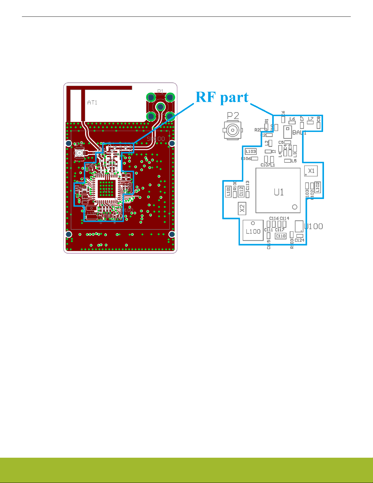
• The compact RF part of the designs (excluding the 50 Ω single-ended antenna) is highlighted by a blue frame, and it is strongly
recommended to use the same framed RF layout in order to avoid any possibility of detuning effects. The figure below shows the
framed compact RF part of the designs.
Figure 1.1. Top Layer of the Radio Board (Left Side) and Assembly Drawing of the RF Part (Right Side)
• The layout of the MCU VDD filtering capacitors should also be copied from the reference design as much as possible. When layouts
cannot be followed as shown by the reference designs (due to PCB size and shape limitations), the layout design rules described in
the following sections are recommended.
silabs.com | Building a more connected world. Rev. 0.5 | 2
Page 3
AN928.1: EFR32 Series 1 Layout Design Guide
Design Recommendations When Using EFR32 Series 1 Wireless MCUs
1.1 Matching Network Types for the 2.4 GHz EFR32 Series 1 Wireless MCU
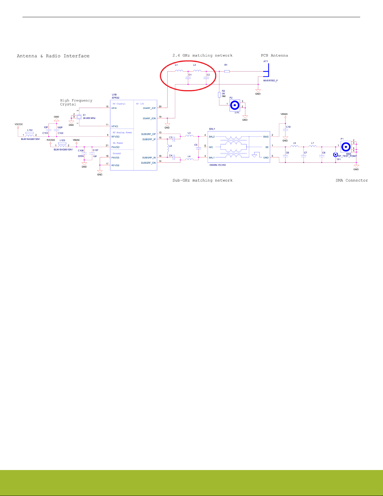
The antenna and radio interface schematic for the EFR32 Series 1 Dual-band (2.4 GHz and sub-GHz) Reference Radio Board is shown
in the figure below, the 2.4 GHz matching is highlighted by a red frame.
Figure 1.2. Schematic of the RF Section for the EFR32 Series 1 Dual-band Reference Radio Board (2.4 GHz Matching is High-
lighted)
Note: Matching network component values for the 2.4 GHz frequency band should be chosen based on power range. For the correct
component values, refer to the reference designs. The 2.4 GHz-only EFR32 and the dual-band EFR32 have different pinouts. For the
correct pinout information, refer to the data sheet and reference designs.
The 2.4 GHz EFR32 Series 1 wireless MCU can provide maximum +19.5 dBm power. All EFR32 Series 1 reference designs for 2.4
GHz use a series-L parallel-C ladder structured matching network. For low power applications (≤10 dBm) a 2-element L-C network is
sufficient, while high power solutions (>10 dBm) require a 4-element match.
It is not surprising that the increased TX output power of the EFR32 devices is accompanied by a corresponding increase in the absolute level of harmonic signals. Since most regulatory standards (e.g. FCC, ETSI, ARIB etc.) require the harmonic signals to be attenuated below some absolute power level (in watts or dBm), the amount of low-pass filtering required is generally greater on an RF radioboard using an EFR32 that was designed for higher output power.
In the figure above, there is an additional component (R1) beside the 4-element matching, which is basically not part of the matching
network. The default value of R1 is 0 Ω. On 2.4 GHz-only radio boards that use the 2-element matching network, R1 is replaced by an
inductor to suppress the radiated 2nd harmonic. The proper value varies with antenna structure, in most cases 0 Ω can be used. For a
custom design, it is recommended to leave option for this series element, and its default value should be 0 Ω.
Further details on the 2.4 GHz matching network principles can be found in the application note, AN930.1: EFR32 Series 1 2.4GHz
Matching Guide.
All EFR32 Series 1 radio boards for 2.4 GHz comprise a 50 Ω IFA (Inverted-F Antenna) connected to the 50 Ω output of the matching
network to be able to measure radiated performance. Optional conducted measurements are possible on these radio boards through an
U.FL connector.
silabs.com | Building a more connected world. Rev. 0.5 | 3
Page 4
AN928.1: EFR32 Series 1 Layout Design Guide
Design Recommendations When Using EFR32 Series 1 Wireless MCUs
1.2 Matching Network Types for the sub-GHz EFR32 Series 1 Wireless MCU
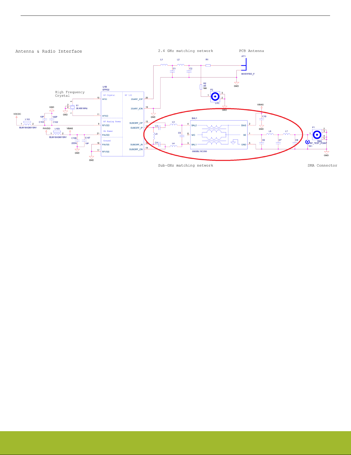
The antenna and radio interface schematic for the EFR32 Series 1 Dual-band (2.4 GHz and sub-GHz) Reference Radio Board is shown
in the figure below, the sub-GHz matching is highlighted by a red frame.
Figure 1.3. Schematic of the RF Section for the EFR32 Series 1 Dual-band Reference Radio Board (sub-GHz Matching is High-
lighted)
Note: Matching network component values should be chosen based on frequency band. Matching network structure can be slightly
different for different frequency bands. For the correct matching network information, refer to the datasheet and reference designs.
The sub-GHz EFR32 Series 1 wireless MCU can provide maximum +19.5 dBm power. All sub-GHz EFR32 matching network consist of
the following sections: impedance transformation circuit, differential to single-ended balun and low-pass filter.
For further details on the sub-GHz matching network principles, refer to the application note, AN923: EFR32 sub-GHz Matching Guide.
All radio boards for sub-GHz comprise an SMA connector, which can be used for conducted measurements or to connect an external
antenna for radiated test purposes.
silabs.com | Building a more connected world. Rev. 0.5 | 4
Page 5

AN928.1: EFR32 Series 1 Layout Design Guide
Guidelines for Layout Design When Using EFR32 Wireless MCUs
2. Guidelines for Layout Design When Using EFR32 Wireless MCUs
Some general guidelines for designing RF-related layouts for good RF performance are:
• For custom designs, use the same number of PCB layers as are present in the reference design whenever possible. Deviation from
the reference PCB layer count can cause different PCB parasitic capacitances, which can detune the matching network from its optimal form. If a design with a different number of layers than the reference design is necessary, make sure that the distance between
the top layer and the first inner layer is similar to that found in the reference design, because this distance determines the parasitic
capacitance value to ground. Otherwise, detuning of the matching network is possible, and fine tuning of the component values may
be required.
• Use as much continuous and unified ground plane metallization as possible, especially on the top and bottom layers.
• Avoid the separation of the ground plane metallization, especially between the ground of the matching network and the RFIC GND
pins / exposed pad.
• Use as many grounding vias (especially near the GND pins) as possible to minimize series parasitic inductance between the ground
pours of different layers and between the GND pins.
• Use a series of GND stitching vias along the PCB edges and internal GND metal pouring edges. The maximum distance between
the vias should be less than lambda/10 of the 10th harmonic (the typical distance between vias on reference radio boards is 40–50
mil). This distance is required to reduce the PCB radiation at higher harmonics caused by the fringing field of these edges.
• For designs with more than two layers, it is recommended to put as many traces (even the digital traces) as possible in an inner
layer and ensure large, continuous GND pours on the top and bottom layers.
• Avoid using long and/or thin transmission lines to connect the RF related components. Otherwise, due to their distributed parasitic
inductance, some detuning effects can occur. Also shorten the interconnection lines as much as possible to reduce the parallel parasitic caps to the ground. However, couplings between neighbor discretes may increase in this way.
• To reduce the coupling between the nearby discrete inductors, avoid placing them in the same orientation.
• Use tapered line between transmission lines with different width (i.e., different impedance) to reduce internal reflections.
• Avoid using loops and long wires to obviate their resonances. They also work well as unwanted radiators, especially at the harmonics.
• Always ensure good VDD filtering by using some bypass capacitors (especially at the range of the operating frequency). The series
self-resonance of the capacitor should be close to the filtered frequency. The bypass capacitor which filters the highest frequency
should be placed closest to the VDD pins of the EFR32. In addition to the fundamental frequency, the crystal/clock frequency and its
harmonics (up to the 3rd) should be filtered to avoid up-converted spurs.
• Connect the crystal case to the ground using many vias to avoid radiation of the ungrounded parts. Do not leave any metal unconnected and floating that may be an unwanted radiator. Avoid leading supply traces close or beneath the crystal or parallel with a
crystal signal or clock trace.
• Place the RF related parts (especially the antenna) far away from the DC-DC converter output and the related DC-DC components.
• Avoid routing GPIO lines close or beneath the RF lines, antenna or crystal, or in parallel with a crystal signal. Use the lowest slew
rate possible on GPIO lines to decrease crosstalk to RF or crystal signals.
• Use as short VDD traces as possible. The VDD trace can be a hidden, unwanted radiator so it is important to simplify the VDD routing
as much as possible and use large, continuous GND pours with many stitching vias. To achieve the simplified VDD routing, try to
avoid star topology of VDD traces (i.e., avoid connecting all VDD traces in one common point).
• Using silkscreen near the antenna could slightly affect the dielectric environment of the antenna. Although this effect is usually negligible, if possible, try to avoid using silkscreen on the antenna or on the antenna copper pour keep out areas.
silabs.com | Building a more connected world. Rev. 0.5 | 5
Page 6
AN928.1: EFR32 Series 1 Layout Design Guide
Guidelines for Layout Design When Using EFR32 Wireless MCUs
2.1 Layout for the 2.4 GHz Frequency Band EFR32 Series 1 Wireless MCU Based on the Dual-band (2.4 GHz and sub-GHz) Reference Radio Board
Examples shown in this section are based on the layout of the EFR32 Series 1 Dual-band Reference Radio Board. The main layout
design concepts are shown with this layout to demonstrate the basic principles. Although these rules will be shown through a design
that uses a 4-element matching, similar design practices should be applied with a 2-element matching network as well. Most of the
layout guidelines in this section are general, and should be applied in the sub-GHz layout design as well.
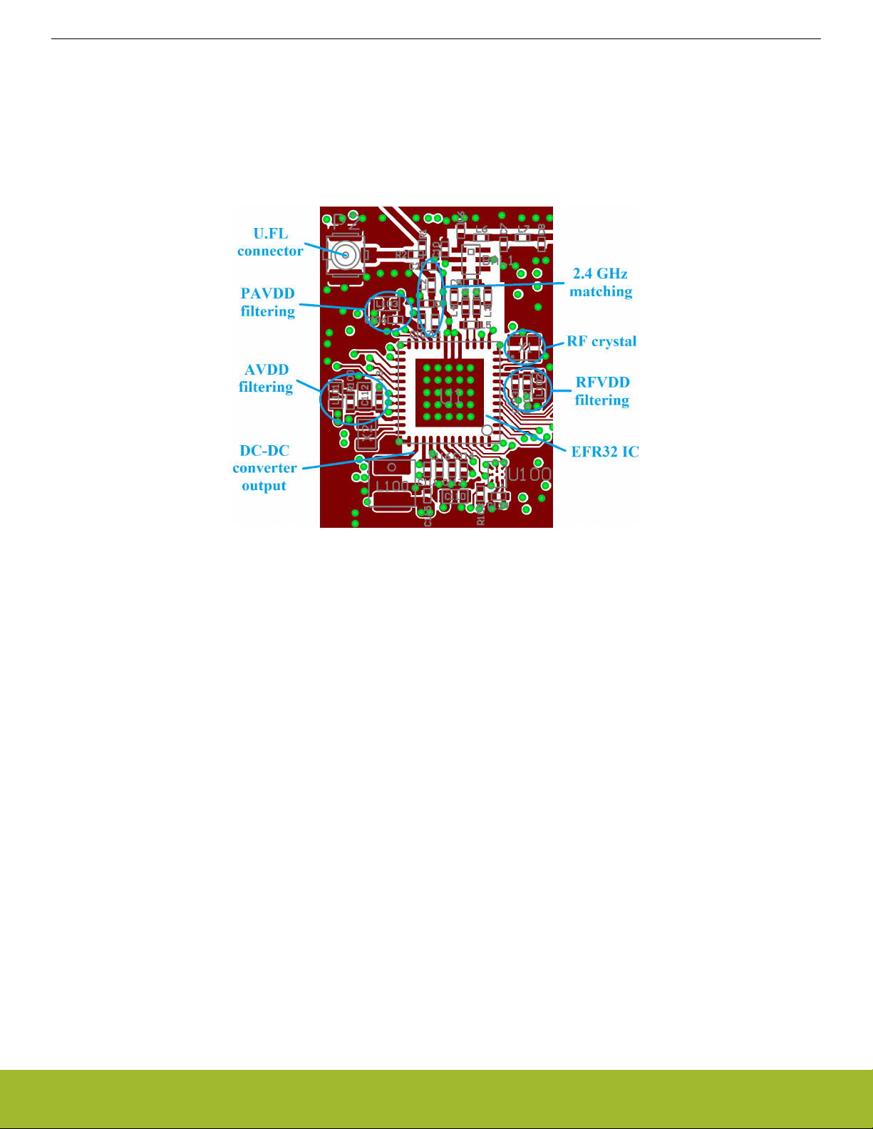
The layout structure for the RF part of the EFR32 Series 1 Dual-band Reference Radio Board is shown in the figure below, the 2.4 GHz
matching is highlighted by a blue frame.
Figure 2.1. Layout of the RF Section for the EFR32 Series 1 Dual-band Reference Radio Board (2.4 GHz Matching is Highligh-
ted)
silabs.com | Building a more connected world. Rev. 0.5 | 6
Page 7

AN928.1: EFR32 Series 1 Layout Design Guide
Guidelines for Layout Design When Using EFR32 Wireless MCUs
2.1.1 Layout Design Guidelines (2.4 GHz)
• The L1 inductor should be placed as close as possible to the 2G4RF_IOP pin (pin 17 on the 7×7 mm sized package) of the EFR32
IC to reduce the series parasitic inductance and avoid any detuning effects.
• The neighboring matching network components should be placed as close to each other as possible to minimize any PCB parasitic
capacitance to the ground and the series parasitic inductances between the components.
• Traces near the GND pins of the capacitors should be thickened to improve the grounding effect in the thermal straps. This minimizes series parasitic inductances between the ground pour and the GND pins. Additional vias placed close to the GND pins of capacitors connect them to the inner/bottom layer GND plane and serve to further reduce these effects.
• The lower-value VDD bypass capacitors (the ones with ~pF values) should be kept as close as possible to the VDD pins (RFVDD,
PAVDD, VREGVDD, AVDD, DVDD, IOVDD).
• To ensure good ground connection, all VDD filtering capacitors should use many vias close to their ground pins. It is also recommended that the GND return path between the GND vias of the VDD filtering capacitors and the GND vias of the RFIC paddle should not
be blocked in any way; return currents should have a clear and unhindered pathway through the GND plane to the back of the RFIC.
• The exposed pad footprint for the paddle of the EFR32 should use as many vias as possible to ensure good grounding and heat sink
capability. In the reference designs there are 25 vias for the 7×7 mm sized package ICs, each with 10 mil diameter.
• The RF crystal should be placed as close as possible to the HFXI and HFXO pins of the ERF32 IC in order to minimize wire parasitic
capacitances and any frequency offsets.
• Use at least 0.5 mm separation between traces/pads to the adjacent GND pour in the areas of the matching networks. This technique will minimize the parasitic capacitance and reduce the detuning effects.
• If space allows, the nearby inductors of the matching network should be kept perpendicular to each other to reduce coupling between stages. This helps to improve filter attenuation at higher harmonic frequencies. The series matching / filtering inductors can be
placed one after another or perpendicular to each other.
• Couplings through the ground can occur between nearby filtering capacitors (especially at high harmonics) and decrease the effectiveness of low-pass filtering, causing higher conducted and radiated harmonics. To avoid possible high harmonic levels, it is recommended to connect the nearby harmonic filtering capacitors to ground planes on different sides of the transmission line.
The figure below demonstrates the above listed layout design recommendations on the reference radio board.
Figure 2.2. EFR32 Series 1 Layout Design Rules (Dual-band Reference Layout Top Layer)
• To achieve good RF ground on the layout, it is recommended to add large, continuous GND metallization on the top layer in the area
of the RF section (at a minimum). Better performance may be obtained if this is applied to the entire PCB. To provide a good RF
ground, the RF voltage potentials should be equal along the entire GND area as this helps maintain good VDD filtering. Gaps should
ideally be filled with GND metal and the resulting sections on the top and bottom layers should be connected with as many vias as
possible. The reason for not using vias on the entire GND section is due to the restrictions of the actual radio board design. These
restrictions include traces routed on other layers or components on the bottom side, which are not shown in the figure above.
silabs.com | Building a more connected world. Rev. 0.5 | 7
Page 8

AN928.1: EFR32 Series 1 Layout Design Guide
Guidelines for Layout Design When Using EFR32 Wireless MCUs
• The area beneath the RF chip and the matching network (on the first inner layer) should be filled with continuous ground metal as it
will show good ground reference for the matching network and will ensure a good, low impedance return path to the RF chip’s
ground as well. Board routing and wiring should not be placed in this region to prevent coupling effects with the matching network. It
is also recommended that the GND return path between the GND vias of the TX/RX matching network and the GND vias of the
RFIC paddle should not be blocked in any way; the return currents should see a clear, unhindered pathway through the GND plane
to the back of the RFIC.
• Use an isolating ground metal between the crystal and VDD traces to avoid any detuning effects on the crystal caused by the nearby
power supply and to avoid the leakage of the crystal/clk signal and its harmonics to the supply lines.
Figure 2.3. EFR32 Series 1 Layout Design Rules (Dual-band Reference Layout Top and Inner Layer 1)
• Use as many parallel grounding vias at the GND metal edges as possible, especially at the edge of the PCB and along the V
trace, to reduce their harmonic radiation caused by the fringing field.
Figure 2.4. GND Vias at PCB Edges on the EFR32 Series 1 Dual-band Reference Layout
DD
• If necessary, a shielding cap can be used to shield the harmonic radiations of the PCB; in that case, the shielding cap should cover
all of the RF-related components (excluding the antenna).
silabs.com | Building a more connected world. Rev. 0.5 | 8
Page 9

AN928.1: EFR32 Series 1 Layout Design Guide
Guidelines for Layout Design When Using EFR32 Wireless MCUs
The ideal layer consistency for PCBs with more than two layers is as follows:
Top layer: Use as much continuous solid GND metallization as possible with many vias.
First inner layer: Use continuous, unified GND metallization beneath the RF part; wires can be routed beneath the non-
RF parts if necessary.
All other inner layers: Route as many (supply and digital) traces on these layers as possible.
Bottom layer: This layer should be unified GND metal; route traces on this layer only if necessary.
The following figure illustrates layer consistency on the layout of the EFR32 Series 1 Dual-band Reference Radio Board.
Top Inner 1 Inner 2 Bottom
Figure 2.5. Layer Consistency on the Layout of the EFR32 Series 1 Dual-band Reference Radio Board
Note: The sub-GHz matching has some special layout recommendations for the individual PCB layers, which will be discussed in
2.2.1 Layout Design Guidelines (sub-GHz).
• Route traces (especially the supply and digital lines) on inner layers for boards with more than two layers.
• Avoid placing the supply lines close to the PCB edge.
• To reduce sensitivity to PCB thickness variations, use 50 Ω grounded coplanar lines where possible for connecting the antenna or
the U.FL connector to the matching network. This also reduces radiation and coupling effects. A general rule is to use 50 Ω transmission lines where the length of the RF trace is longer than λ/16 at the fundamental frequency.
• The interconnections between elements are not considered transmission lines since their lengths are much shorter than the wavelength, and, thus, their impedances are not critical. As a result, their recommended width is equal to the width of the pad of the applied components. In this way, reflections at pad-trace transitions can be prevented, and parasitic capacitances to ground can be
minimized. Examples for the trace dimensions are shown in the table below.
• Use many vias near the coplanar lines in order to minimize radiation.
silabs.com | Building a more connected world. Rev. 0.5 | 9
Page 10

AN928.1: EFR32 Series 1 Layout Design Guide
Guidelines for Layout Design When Using EFR32 Wireless MCUs
The following figure demonstrates the 50 Ω grounded coplanar lines on the layout of the EFR32 Series 1 Dual-band Reference Radio
Board.
Figure 2.6. 50 Ω Grounded Coplanar Lines on the Layout of the EFR32 Series 1 Dual-band Reference Radio Board
Table 2.1. Parameters for 50 Ω Grounded Coplanar Lines
Lines Parameters
f 2.4 GHz, sub-GHz
T 0.018-0.035 mm
ε
r
4.6
H 0.325 mm
G 0.25 mm
W 0.45 mm
Notes:
1. Characteristic impedance is not “super sensitive” to the gap value. It should be between 0.25 and 0.4 mm to have 47 through 53 Ω
impedance.
2. Different impedance calculators may yield slightly different results.
3. H is the distance between the top and the first inner layer.
Figure 2.7. Grounded Coplanar Line Parameters
silabs.com | Building a more connected world. Rev. 0.5 | 10
Page 11

AN928.1: EFR32 Series 1 Layout Design Guide
Guidelines for Layout Design When Using EFR32 Wireless MCUs
2.2 Layout for the sub-GHz Frequency Band EFR32 Series 1 Based on the Dual-band (2.4 GHz and sub-GHz) Reference Radio Board
Examples shown in this section are based on the layout of the EFR32 Series 1 Dual-band Reference Radio Board. The main layout
design concepts are shown with this layout to demonstrate the basic principles. Although these rules will be shown through a design
that uses a 915 MHz matching, similar design practices should be applied with matching networks for other sub-GHz frequencies as
well.
The layout structure for the RF part of the EFR32 Series 1 Dual-band Reference Radio Board is shown in the figure below, the subGHz matching is highlighted by a blue frame.
Figure 2.8. Layout of the RF Section for the EFR32 Series 1 Dual-band Reference Radio Board (sub-GHz Matching is Highligh-
ted)
silabs.com | Building a more connected world. Rev. 0.5 | 11
Page 12

AN928.1: EFR32 Series 1 Layout Design Guide
Guidelines for Layout Design When Using EFR32 Wireless MCUs
2.2.1 Layout Design Guidelines (sub-GHz)
• Due to the differential TX/RX pins of the sub-GHz EFR32 Series 1 wireless MCU, the traces that connect the first TX/RX component(s) with the TX output / RX input of the chip must be routed on different layers. To decrease the parasitic capacitance towards
the ground, it is recommended to apply a keepout on all inner layers beneath the area of the RX matching network. On the first inner
layer, the area beneath the remainder sub-GHz matching network (balun and low-pass filter) should be filled with ground metal.
Traces can be routed beneath the area of the balun and low-pass filter sections on all other inner layers.
• Use the shortest traces possible to connect the first RX matching network component with the RX input pins of the chip. As a result,
the first TX matching network components can be connected only with relatively long traces.
• No traces should be routed on the layer beneath the traces that connects the first TX matching components with TX pins.
• It is recommended to add an isolating ground metal with many vias between the 2.4 GHz and sub-GHz matching networks.
The following figures illustrate layer consistency around the area of the matching networks on the layout of the EFR32 Series 1 Dualband Reference Radio Board.
Figure 2.9. Layout of the Matching Area on the EFR32 Series 1 Dual-band Reference Layout — Top layer
Figure 2.10. Layout of the Matching Area on the EFR32 Series 1 Dual-band Reference Layout — Inner layer 1
Figure 2.11. Layout of the Matching Area on the EFR32 Series 1 Dual-band Reference Layout — Inner layer 2
silabs.com | Building a more connected world. Rev. 0.5 | 12
Page 13

AN928.1: EFR32 Series 1 Layout Design Guide
Guidelines for Layout Design When Using EFR32 Wireless MCUs
Figure 2.12. Layout of the Matching Area on the EFR32 Series 1 Dual-band Reference Layout — Bottom layer
silabs.com | Building a more connected world. Rev. 0.5 | 13
Page 14

3. Checklists
3.1 Main Layout Design Principles
1. Is the number of PCB layers the same
as in the reference design? Or at a minimum, is the distance between the top
and first inner layers similar?
2. Are the neighboring matching network
components as close to each other as
possible?
3. Is the trace width (near) the same as
pad width for connecting nearby components?
4. Are the series matching / filtering inductors placed one after another or perpendicular to each other?
5. Is the RF crystal as close to the XTAL
pins of the EFR32 IC as possible?
6. Does ground metal exist between the
crystal and the RFVDD feed?
AN928.1: EFR32 Series 1 Layout Design Guide
Checklists
7. Are the smallest value VDD filtering capacitors kept as close as possible to the
VDD pins (RFVDD, PAVDD, VREGVDD,
AVDD, DVDD, IOVDD) of the EFR32?
8. Are there multiple thermal straps used
with the shunt capacitors?
9. Do the ground pins of the shunt capacitors use multiple vias?
10. Does the exposed pad footprint use multiple vias?
11. Is there at least 0.5 mm separation in
the matching between the traces/pads
and the GND metal?
12. Is wiring and routing avoided on (basically) the first inner (GND) layer between
the grounding vias of VDD filtering capacitors and the exposed pad of the
EFR32 IC?
silabs.com | Building a more connected world. Rev. 0.5 | 14
Page 15

13. Are supply and digital traces routed on
inner layers? Or at a minimum, are the
supply lines surrounded by ground metal
with many GND vias if routed on the top
or the bottom layers?
14. Is placing supply or digital lines close to
the PCB edge avoided?
15. Is large, continuous GND metallization
added to at least the RF sections using
as many GND vias as possible?
16. Are the GND metal edges closed by
"stitching vias" where possible, with a
via distance less than lambda/10 of the
highest (usually 10th) critical harmonic
frequency?
AN928.1: EFR32 Series 1 Layout Design Guide
Checklists
17. Are 50 Ω grounded coplanar lines used
for RF traces longer than λ/16 at the fundamental frequency?
18. Are there vias at the ground metallization near the 50 Ω transmission lines?
19. Are the RF related parts (especially the
antenna) placed far away from the DCDC converter output and the related DCDC components?
silabs.com | Building a more connected world. Rev. 0.5 | 15
Page 16

3.2 Additional Concerns for the 2.4 GHz Matching Network
20. Is the first matching network component
(L1) placed as close to the corresponding TX pin as possible?
21. Are the nearby harmonic filtering capacitors connected to ground planes on different sides of the transmission line?
22. Is the area on the first inner layer beneath the RF chip and the matching network filled with continuous GND metal,
and was wiring and routing avoided in
this region?
AN928.1: EFR32 Series 1 Layout Design Guide
Checklists
silabs.com | Building a more connected world. Rev. 0.5 | 16
Page 17

3.3 Additional Concerns for the sub-GHz Matching Network
23. Is the first RX matching network component placed as close to the RX pins as
possible?
24. Is an isolating ground metal with many
vias added between the 2.4 GHz and
sub-GHz matching network?
25. Is a keepout applied on all inner layers
beneath the area of the RX matching
network?
26. Is the area on the first inner layer beneath the balun and low-pass filter filled
with continuous GND metal, and was
wiring and routing avoided in this region?
AN928.1: EFR32 Series 1 Layout Design Guide
Checklists
27. Is wiring and routing avoided on the layer beneath the traces that connect the
first TX matching network components
with TX pins?
silabs.com | Building a more connected world. Rev. 0.5 | 17
Page 18

Simplicity Studio
One-click access to MCU and
wireless tools, documentation,
software, source code libraries &
more. Available for Windows,
Mac and Linux!
IoT Portfolio
www.silabs.com/IoT
Disclaimer
Silicon Labs intends to provide customers with the latest, accurate, and in-depth documentation of all peripherals and modules available for system and software implementers using or
intending to use the Silicon Labs products. Characterization data, available modules and peripherals, memory sizes and memory addresses refer to each specific device, and "Typical"
parameters provided can and do vary in different applications. Application examples described herein are for illustrative purposes only. Silicon Labs reserves the right to make changes
without further notice to the product information, specifications, and descriptions herein, and does not give warranties as to the accuracy or completeness of the included information.
Without prior notification, Silicon Labs may update product firmware during the manufacturing process for security or reliability reasons. Such changes will not alter the specifications or the
performance of the product. Silicon Labs shall have no liability for the consequences of use of the information supplied in this document. This document does not imply or expressly grant
any license to design or fabricate any integrated circuits. The products are not designed or authorized to be used within any FDA Class III devices, applications for which FDA premarket
approval is required or Life Support Systems without the specific written consent of Silicon Labs. A "Life Support System" is any product or system intended to support or sustain life and/or
health, which, if it fails, can be reasonably expected to result in significant personal injury or death. Silicon Labs products are not designed or authorized for military applications. Silicon
Labs products shall under no circumstances be used in weapons of mass destruction including (but not limited to) nuclear, biological or chemical weapons, or missiles capable of delivering
such weapons. Silicon Labs disclaims all express and implied warranties and shall not be responsible or liable for any injuries or damages related to use of a Silicon Labs product in such
unauthorized applications.
Trademark Information
Silicon Laboratories Inc.® , Silicon Laboratories®, Silicon Labs®, SiLabs® and the Silicon Labs logo®, Bluegiga®, Bluegiga Logo®, Clockbuilder®, CMEMS®, DSPLL®, EFM®, EFM32®,
EFR, Ember®, Energy Micro, Energy Micro logo and combinations thereof, "the world’s most energy friendly microcontrollers", Ember®, EZLink®, EZRadio®, EZRadioPRO®, Gecko®, Gecko
OS, Gecko OS Studio, ISOmodem®, Precision32®, ProSLIC®, Simplicity Studio®, SiPHY®, T elegesis, the Telegesis Logo®, USBXpress® , Zentri, the Zentri logo and Zentri DMS, Z-Wave®,
and others are trademarks or registered trademarks of Silicon Labs. ARM, CORTEX, Cortex-M3 and THUMB are trademarks or registered trademarks of ARM Holdings. Keil is a registered
trademark of ARM Limited. Wi-Fi is a registered trademark of the Wi-Fi Alliance. All other products or brand names mentioned herein are trademarks of their respective holders.
Silicon Laboratories Inc.
400 West Cesar Chavez
Austin, TX 78701
USA
SW/HW
www.silabs.com/simplicity
Quality
www.silabs.com/quality
Support and Community
community.silabs.com
http://www.silabs.com
 Loading...