

Page 1
AN930.2: EFR32 Series 2 2.4 GHz
Matching Guide
The EFR32 Series 2 devices include chip variants that provide
2.4 GHz-only operation. In addition, the EFR32xG21 chips are
only available in a 4x4 mm 32-pin QFN package while the
EFR32xG22 parts have both 32- and 40-pin package variants
available (QFN32, TQFN32, QFN40). This application note describes the matching techniques applied to the EFR32 Series 2
Wireless Gecko Portfolio in the 2.4 GHz band.
For information on PCB layout requirements for proper 2.4 GHz operation, refer to application note, AN928.2: EFR32 Series 2 Layout Design Guide.
KEY POINTS
• Description of the applied 2.4 GHz
matching networks and techniques for the
EFR32 Series 2 devices
• Detailed discussion of the design steps
and design examples
• Measured TX fundamental and harmonic
performance
• Measured receive sensitivity values
silabs.com | Building a more connected world. Rev. 0.6
Page 2

1. Device Compatibility
This application note supports the following devices:
EFR32 Wireless Gecko Series 2:
• EFR32MG21
• EFR32MG22
• EFR32BG21
• EFR32BG22
• EFR32FG22
AN930.2: EFR32 Series 2 2.4 GHz Matching Guide
Device Compatibility
silabs.com | Building a more connected world. Rev. 0.6 | 2
Page 3
AN930.2: EFR32 Series 2 2.4 GHz Matching Guide
Introduction
2. Introduction
This application note is intended to help users achieve the best 2.4 GHz RF match for targeted applications. It describes the details of
matching network design procedures and presents additional test results.
Thorough derivations of four different matching options are presented for EFR32xG21:
• 4-element discrete LC match for up to 0 dBm power levels
• 3-element discrete LC match for up to +10 dBm power levels
• 5-element discrete LC match for up to +20 dBm power levels
• 4-element combined discrete LC match for both +10 and 0 dBm power levels
A 4-element discrete LC match for up to +6 dBm power levels is also presented for EFR32xG22.
The 4x4 mm, 32-pin 2.4 GHz-only version's package pinouts are shown in the figures below for each EFR32xG21 and EFR32xG22
part. The 2.4 GHz RF IO pins are highlighted with a red box.
Figure 2.1. EFR32xG21 2.4 GHz RF IO Pins
silabs.com | Building a more connected world. Rev. 0.6 | 3
Page 4
AN930.2: EFR32 Series 2 2.4 GHz Matching Guide
Introduction
Figure 2.2. EFR32xG22 2.4 GHz RF IO Pin
2.1 Related Literature
Related documentation includes:
• AN928.2: EFR32 Series 2 Layout Design Guide
• AN0002.2: EFM32 and EFR32 Wireless Gecko Series 2 Hardware Design Considerations
silabs.com | Building a more connected world. Rev. 0.6 | 4
Page 5
AN930.2: EFR32 Series 2 2.4 GHz Matching Guide
RF Architecture Overview
3. RF Architecture Overview
3.1 EFR32xG21 RF Front-End Overview
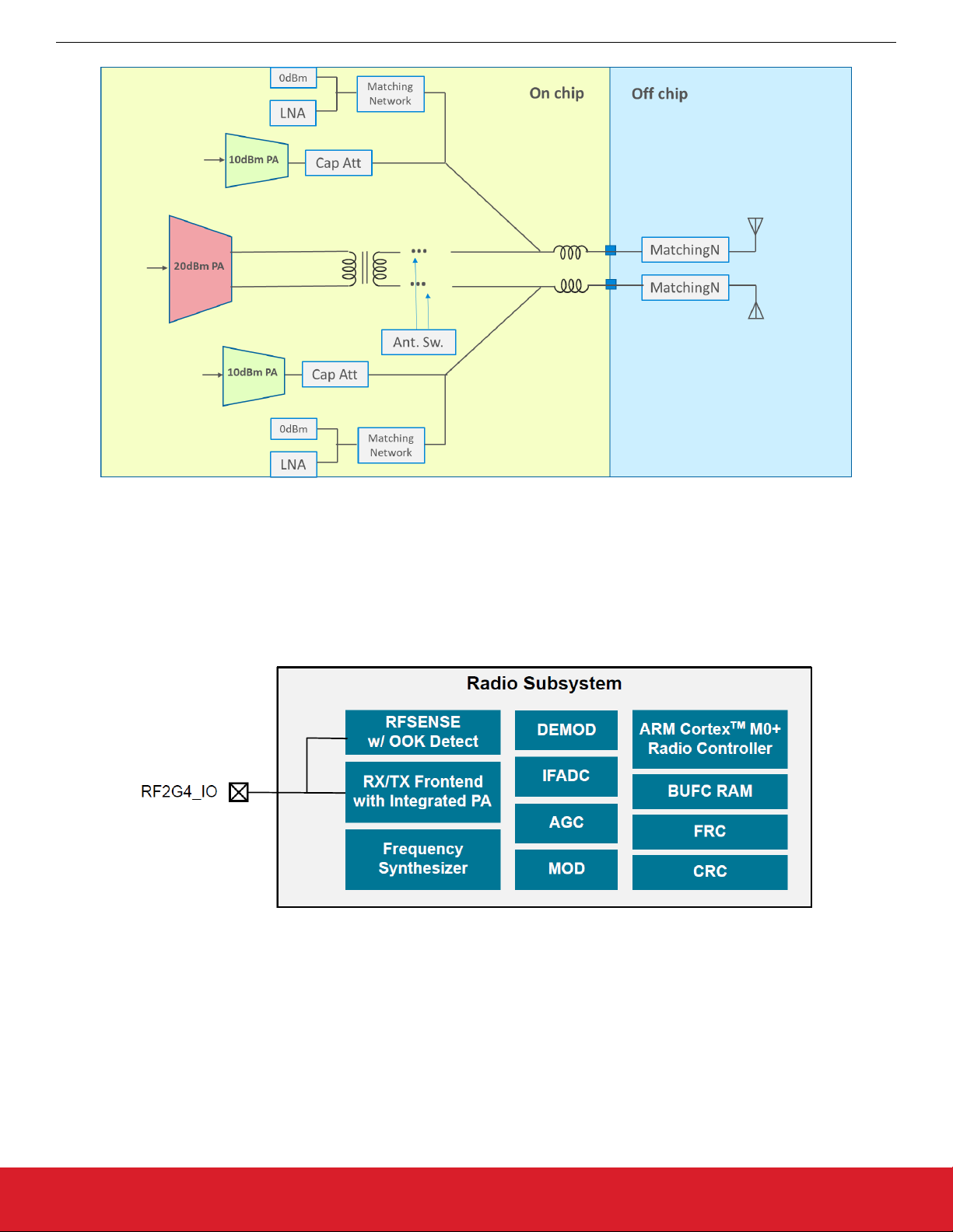
The EFR32 Series 2 xG21 chip family has 2.4 GHz RF front ends only. The 2.4 GHz RF front-end architecture is shown in the figure
below. The 2.4 GHz antenna interface consists of two pins (RF2G4_IO1 and RF2G4_IO2) that interface directly to the on-chip BALUN.
Figure 3.1. 2.4 GHz RF Front-end Configuration
Several changes compared to the EFR32 Series 1 chip variants are highlighted below:
• New RF front-end topology: Three PAs included that require an optimal load impedance for each TX power level, i.e., different
matches are required per max TX power.
• Power supply scheme: There is no on-chip DCDC converter available. Optimized for mains-power applications.
• Pre-Regulator for the Power Amplifiers: Linear regulator with an input of PAVDD and output of PA blocks. Regulates to a target voltage when PAVDD > Vtarget. Follows supply with a ~30 mV offset when PAVDD ≤ Vtarget (and PA power will trail off also).
• For +10 and 0 dBm PA modes: Vtarget = 1.8 V.
• For +20 dBm PA mode: Vtarget = 3.3 V.
• RFSENSE removed, instead a wide-band power sensing block introduced for better out-of-band blocker detection and coexistence
performance.
The on-chip part of the front-end comprises three PA structures optimized for the TX power levels of 0, 10, and 20 dBm, two differential
LNAs, and an integrated balun. Each PA is biased through the PAVDD pin. Externally, a single-ended matching network and harmonic
filtering are required.
• Differential Class-AB mode PA and an internal balun for TX power of +20 dBm
• Single-ended Class-D mode PA for TX power of +10 dBm
• Single-ended Class-D mode PA for TX power of 0 dBm
• Two LNAs
• Two RF IO ports available: Internal switches ground one of the two sides to create single-ended inputs / outputs on either RFIO pin.
silabs.com | Building a more connected world. Rev. 0.6 | 5
Page 6
AN930.2: EFR32 Series 2 2.4 GHz Matching Guide
RF Architecture Overview
Figure 3.2. 2.4 GHz RF Front-end Block Diagram
3.2 EFR32xG22 RF Front-End Overview
The EFR32 Series 2 xG22 chip family has 2.4 GHz RF front ends only. The radio subsystem is shown in the figure below. The RF frontend consists of an integrated LNA and two separate PAs with an internal switch to select between them, while one RF IO port is available (RF2G4_IO) at a chip pin.
Figure 3.3. EFR32xG22 Radio Subsystem
A few highlights on the RF front-end blocks:
• Two separate Class-D PAs, optimized for maximum TX power levels of 0 and +6 dBm.
• Each PA is biased through the PAVDD pin
• Externally, a single-ended matching network and harmonic filtering are required
• Power supply scheme: An on-chip, dc-dc converter is available, so this chip variant is optimized for low-power applications with high
efficiency.
silabs.com | Building a more connected world. Rev. 0.6 | 6
Page 7

AN930.2: EFR32 Series 2 2.4 GHz Matching Guide
2.4 GHz RF Matching Design Steps
4. 2.4 GHz RF Matching Design Steps
2.4 GHz RF matching design for EFR32 chips consists of the following steps:
1. Determine the optimum termination impedance for the PA. Note that different matching topologies are recommended for different
TX power levels as shown in the Introduction section.
2. Choose the RF matching topology.
3. Create the initial design with ideal, loss-free elements. This ideal design can be used as a starting point for a design with parasitics.
4. Design with parasitics and losses. At 2.4 GHz, the parasitics of the SMD elements and the pcb have a major effect, so tuning/
optimization of the design is required. Here an optional EM simulation can be done, but simulations with well-estimated pcb parasitics and SMD equivalent models usually give adequate results.
5. Conduct bench testing and tuning.
4.1 Determining the Optimum Termination Impedance for the PA
The first step of the matching design procedure is to determine the optimum termination impedance at the PA. The realized matching
network should present this impedance for the PA at the RF2G4_IO1/2 pin if 50 Ω termination is applied at the antenna port.
The RF2G4_IO1/2 RF port termination determines the major RF parameters, such as the delivered PA power and harmonic content in
TX mode or the sensitivity in RX mode. As part of the design process, the goal is to deliver maximum power to a 50 Ω output termination (e.g., to a 50 Ω antenna) in TX mode. In addition, proper harmonic suppression and good RX sensitivity in reception mode are
required.
4.1.1 EFR32xG21 Optimum PA Load Impedance
The design target of optimum load impedance looking from the PA to the antenna is 14 + j5 Ω at the PA. However, the optimum termination impedance for both delivering the desired power and achieving the best PA efficiency in TX mode is determined by load-pull
testing. The optimum termination impedance at the chip pin is determined for each PA of the EFR32xG21 parts and it slightly differs for
the different power levels, i.e., for the +20, +10, and 0 dBm PAs, and also differs from the design target at the PA due to bonding wire
inductances and parasitics. This termination impedance has to be shown by the matching network at the PA side if its antenna output is
terminated with a 50 Ω load. The optimum termination impedance at chip RF2G4_IO pin is the following:
• For the +20 dBm PA: Zload_opt = 12.6 - j11 Ω
• For the +10 dBm PA: Zload_opt = 12.2 - j8.3 Ω
• For the 0 dBm PA: Zload_opt = 17.4 + j3.9 Ω
The load-pull curves for each PA are shown in 6. Appendix 1 PA Optimum Termination Impedance on EFR32xG21.
Applications with one antenna typically require using only one of the RF IO ports available on the EFR32xG21 parts, in which case the
recommended active RF IO port is RF2G4_IO2. Because this pin has a shorter on-chip, internal connection to the PA blocks so slightly
lower parasitics appear on this pin.
The proper impedance at one of the single-ended RF2G4_IO pins also depends on the loading of the other RF2G4_IO pin. To keep its
effect negligible, for applications with one antenna with both +10 and +20 dBm PAs, it is recommended to directly tie the un-used
RF2G4_IO pin back to the center GND pad of the chip. However, the 0 dBm PA requires to be DC blocked externally so the method
described for the +10 and +20 dBm PAs doesn't work. The 0 dBm PA recommended match includes a series capacitor in the RF path
but for proper operation a DC-blocking 0.5pF capacitor to GND needs to also be used on the unused RF port. Silicon Labs' reference
radio boards are suitable and optimized to be used with the +10 and +20 dBm PAs because of the short between the chip pin and
center GND pad under the chip. More detailed information about proper layout design can be found in application note, "AN928.2:
EFR32 Series 2 Layout Design Guide".
In real radio links, the TX power and the receiver sensitivity together (i.e., the link budget) determine the range. So, with the applied TX
termination impedance, the impedance match in RX mode should also be acceptable. Fortunately, the RX sensitivity is quite immune to
impedance variations. The sensitivity variation is less than 0.5 dB if the termination changes from 50 Ω to the PA optimum impedance
(Zload_opt) given above.
silabs.com | Building a more connected world. Rev. 0.6 | 7
Page 8

AN930.2: EFR32 Series 2 2.4 GHz Matching Guide
2.4 GHz RF Matching Design Steps
4.1.2 EFR32xG22 Optimum PA Load Impedance
The design target of optimum load impedance looking from the PA to the antenna is 50 Ω at the PA for both 0 and +6 dBm PA. However, the optimum termination impedance at the chip pin determined for each PA of the EFR32xG22 parts differs from the design target at
the PA due to bonding wire inductances and parasitics. Also, the output match plus low-pass filter (LPF) section is designed to enhance
the suppression of the 2nd- and 3rd-order harmonics. Thus, the optimum termination impedance at the chip pin is about 37 + j5 Ω for
both 0 and +6 dBm PA and this impedance has to be shown by the matching network at the PA side if its antenna output is terminated
with a 50 Ω load.
Because the optimum termination impedance is the same for both 0 and +6 dBm PA, the matching network is also identical for these
different power levels. Silicon Labs provides radio boards with one matching network applied, however, the series dc-blocking capacitor
in the match plus LPF section must be needed only when the 0 dBm PA is being utilized.
4.2 Choosing the RF Matching Topology
The second step of the matching design procedure is to choose the appropriate RF matching topology.
In addition to creating an optimum termination impedance on the IC side, the matching solution must exhibit sufficiently robust harmonic
filtering characteristics to comply with emissions standards. There are many different types of RF matching topologies. Separate matching and harmonic filtering sections can be utilized, or they can be combined in one circuit. To minimize the number of elements, all
matches presented here are of the combined type, with low-pass circuits employed for their inherent harmonic suppression characteristics.
Four 2.4 GHz matching topologies for EFR32xG21 are presented here:
• 4-element discrete LC match for the 0 dBm PA, i.e., for power levels equal or below 0 dBm
• 4-element combined discrete LC match for both 0 and +10 dBm PA, i.e., for power levels equal or below +10 dBm
• 3-element discrete LC match for the +10 dBm PA, i.e., for power levels equal or below +10 dBm, but not suitable to operate with the
0 dBm PA (i.e., equal or below 0 dBm the required PA to be used is still the +10 dBm PA which has less power efficiency at that
lower power range)
• 5-element discrete LC match for the +20dBm PA, i.e., for power levels equal or below +20 dBm (not suitable to operate with the 0
dBm PA)
For EFR32xG22, a single 4-element discrete LC match is provided that is optimized for both 0 and +6 dBm PA, i.e., for any power level
available with this part.
4.3 Initial Design with Ideal, Loss-Free Elements
After choosing the appropriate topology for the application based on the TX power level requirements, the third step of the matching
design procedure is to generate a lumped element schematic of the match with ideal loss-free elements and without PCB parasitics.
The matching circuit should show an input impedance of Zload_opt at the RF IO port of the chip while it is terminated by 50 Ω load at its
output (ANT port). The impedance procedure is shown in the next sections, where, for simplification, the matching design is started
from a termination impedance (ZL) which is the complex conjugate of the Zload_opt impedance. The reason is that the matching network will show the required Zload_opt impedance at its RF port only if it is perfectly matched there to a termination impedance which is
the complex conjugate of the Zload_opt impedance.
The matching design process starts with a simplified case in which all losses and parasitics are eliminated. Here, parasitic-free ideal
capacitors and inductors are used, and there are no PCB losses or parasitics. The real-world case can be derived later from this ideal
design by means of incremental tuning and optimization.
silabs.com | Building a more connected world. Rev. 0.6 | 8
Page 9

AN930.2: EFR32 Series 2 2.4 GHz Matching Guide
2.4 GHz RF Matching Design Steps
4.4 Design with Parasitics and Losses
Silicon Labs reference designs utilize lumped elements in the RF matching network. At the operating frequency band of 2.4 GHz, the
used SMD components and also the PCB parasitic effects need to be taken into account during the matching network design. The SMD
components at these high-frequency ranges behave as a resonator. A capacitor can be realized by a series RLC resonant circuit,
meanwhile an inductor’s equivalent circuit represents a parallel RLC resonant circuit. Regarding the PCB parasitic effects, the series
traces can be modeled as transmission lines with distributed L-C components, and can have considerable series parasitic inductance,
while an SMD pad can behave as a parallel parasitic capacitance. For more details on the SMD parasitic descriptions and the rough
estimation of PCB parasitics, refer to the application note, AN930.1: EFR32 Series 1 2.4 GHz Matching Guide, and the SMD manufacturer website at www.murata.com, in regards to the appropriate SMD equivalent circuits.
The SMD components with different sizes have different parasitics, so it is also important to calculate with the appropriate values. Silicon Labs reference designs use SMD 0201 components.
The PCB parasitics also have effects on the RF performance versus tuned component values of the matching network. Silicon Labs
reference design matching network component values are typically given with a 4-layer PCB with a separation of about 300 µm
between the top (component-side) and first inner layer. This distance mostly determines the parasitics capacitance and via inductance,
which influences the return-path impedance between the matching network and chip GND (especially at the harmonics). Also, the series trace placed between the chip pin and matching network is part of the match, the dimensions of which should be followed carefully
from Silicon Labs reference designs. Refer to AN928.2: EFR32 Series 2 Layout Design Guide for more layout details.
In the case of using different PCB stack-up (e.g. 2-layer PCB with board thickness > 300 um), the matching network component values
need tuning to keep the RF performance values, especially the harmonic suppressions.
The recommended matching network for the RF port(s) of each part is shown in the section Recommended Matching Networks. The
circuit provides the optimum impedance load for the EFR32xG2x part while ensuring sufficient harmonic suppression. Some of the
shunt capacitors are tuned to have self-resonances at the frequency ranges falling close to TX harmonics and therefore, they provide
enhanced attenuation at specific harmonics. The impedance transformation procedure for each PA of EFR32xG21 is shown in the
Smith Chart figures below. The impedance transformation procedure for the PAs of EFR32xG22 is not separately shown here on the
Smith Chart because the matching network is basically a tuned LPF between 50 Ω loads.
Figure 4.1. EFR32xG21 4-element Match with SMD and PCB Layout Parasitics Tuned for the 0 dBm Power Level Optimum
silabs.com | Building a more connected world. Rev. 0.6 | 9
Page 10

AN930.2: EFR32 Series 2 2.4 GHz Matching Guide
2.4 GHz RF Matching Design Steps
Figure 4.2. EFR32xG21 3-element Match with SMD and PCB Layout Parasitics Tuned for the 10 dBm Power Level Optimum
Figure 4.3. EFR32xG21 5-element Match with SMD and PCB Layout Parasitics Tuned for the 20 dBm Power Level Optimum
silabs.com | Building a more connected world. Rev. 0.6 | 10
Page 11
AN930.2: EFR32 Series 2 2.4 GHz Matching Guide
2.4 GHz RF Matching Design Steps
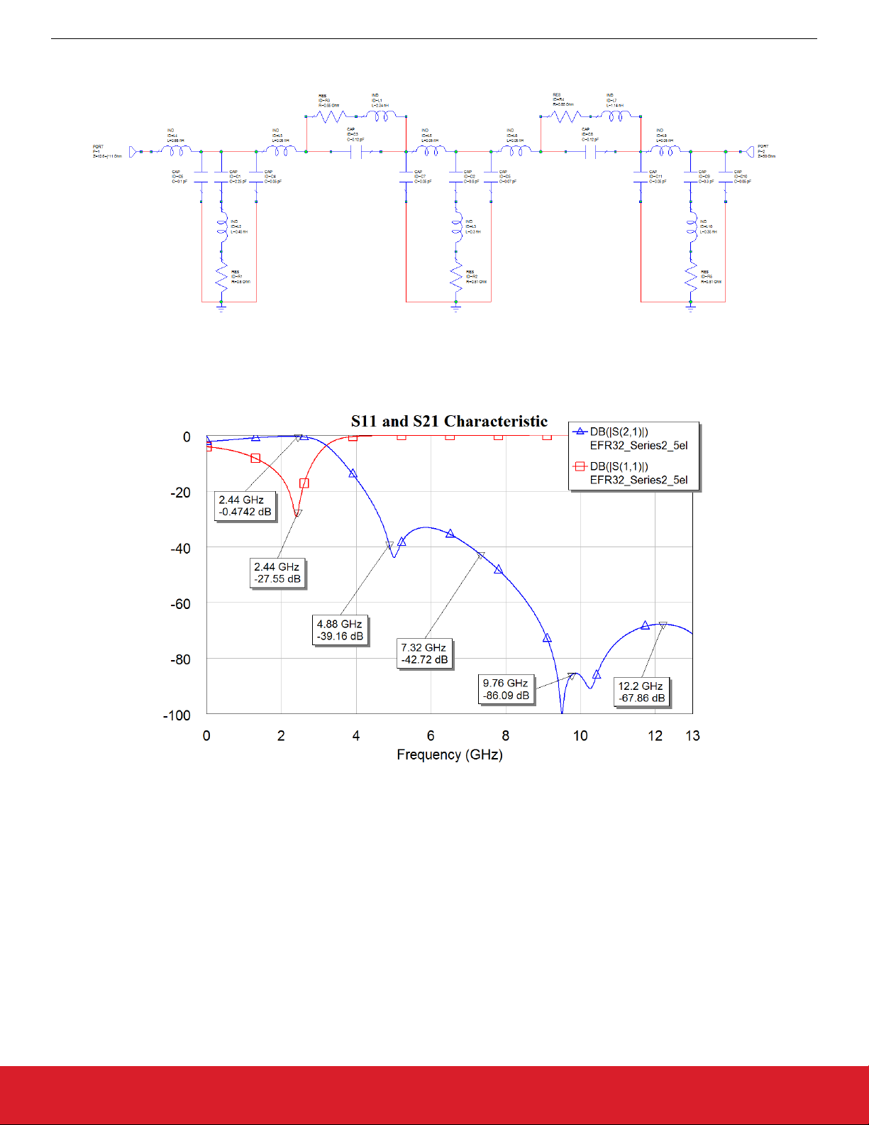
4.5 Simulation Example on the 5-element Match for +20 dBm Power Level on EFR32xG21
Figure 4.4. Discrete Schematic Model of 5-element Match with SMD and PCB Layout Parasitics
Port 1 (left-hand side-end) is the RF2G4_IO chip port/pin where the port impedance (ZL) should be set for the complex conjugate of
optimum load impedance (ZL=Zload_opt*), while the Port 2 (right end) is the 50-ohm antenna port.
Figure 4.5. S11 and S21 Characteristics of 5-element Match for 20 dBm Power Level Optimum
silabs.com | Building a more connected world. Rev. 0.6 | 11
Page 12
5. Recommended Matching Networks
5.1 EFR32xG21 Matching Networks
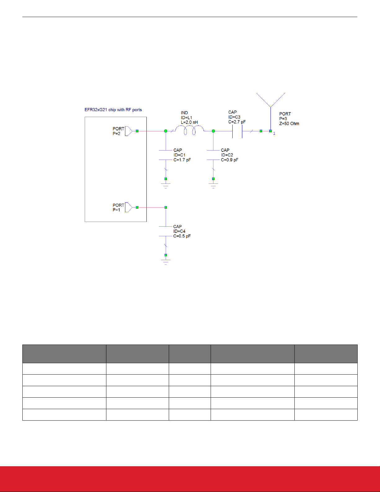
5.1.1 Recommended Matching Network for the 0 dBm PA
AN930.2: EFR32 Series 2 2.4 GHz Matching Guide
Recommended Matching Networks
Figure 5.1. Matching Network Schematic for the 0 dBm PA
It is recommended to use this matching network shown above when the maximum transmitting power requirement is 0 dBm (TX power
≤ 0 dBm), i.e., the application utilizes the 0 dBm PA to achieve the possible best efficiency at that low power regions. Due to the highly
optimized power efficiency, the need of 4-element matching network here is mostly driven by the harmonic suppression requirements.
The unused RF2G4_IO pin needs to be grounded via an (DC-blocking) 0.5 pF capacitor.
Table 5.1. Final SMD Values for the 0 dBm PA (4-element)
Schematic Reference Desig-
nator
C1 1.7 pF ± 0.5 % GRM0335C1H1R7WA01D Murata
L1 2.0 nH ± 0.1 nH LQP03HQ2N0B02D Murata
C2 0.9 pF ± 0.05 pF GRM0335C1HR90WA01D Murata
C3 2.7 pF ± 0.5 % GRM0335C1H2R7WA01D Murata
C4 0.5 pF ± 0.05 pF GRM0335C1HR50WA01D Murata
Component Value Tolerance Part Number Manufacturer
silabs.com | Building a more connected world. Rev. 0.6 | 12
Page 13

5.1.2 Recommended Matching Network for the +10 dBm PA
AN930.2: EFR32 Series 2 2.4 GHz Matching Guide
Recommended Matching Networks
Figure 5.2. Matching Network Schematic for the +10 dBm PA
It is recommended to use the matching network shown above when the maximum transmitting power requirement is +10 dBm (0 dBm <
TX power ≤ +10 dBm), i.e., the application utilizes the +10 dBm PA to achieve the possible best efficiency at that power level state. The
unused RF2G4_IO pin can be grounded directly. Make a short from the pin back to the center exposed pad of the part under the chip.
Table 5.2. Final SMD Values for the +10 dBm PA (3-element)
Schematic Reference Desig-
Component Value Tolerance Part Number Manufacturer
nator
C1 1.9 pF ± 0.5 % GRM0335C1H1R9WA01D Murata
L1 2.1 nH ± 0.1 nH LQP03HQ2N1B02D Murata
C2 0.9 pF ± 0.05 pF GRM0335C1HR90WA01D Murata
silabs.com | Building a more connected world. Rev. 0.6 | 13
Page 14

5.1.3 Recommended Combined Matching Network for Both 0/10 dBm PA
AN930.2: EFR32 Series 2 2.4 GHz Matching Guide
Recommended Matching Networks
Figure 5.3. Combined Matching Network Schematic for both 0 and +10 dBm PA
Use the matching network shown above when the maximum transmitting power requirement is +10 dBm (TX power ≤ +10 dBm). Use 0
dBm PA for the best power efficiency equal or below 0 dBm. Ground the unused RF2G4_IO pin via an (DC-blocking) 0.5 pF capacitor.
Table 5.3. Final SMD Values for the 0/10 dBm PA Match
Schematic Refer-
Component Value Tolerance Part Number Manufacturer
ence Designator
C1 1.9 pF ± 0.5 % GRM0335C1H1R9WA01D Murata
L1 2.1 nH ± 0.1 nH LQP03HQ2N1B02D Murata
C2 0.9 pF ± 0.05 pF GRM0335C1HR90WA01D Murata
C3 2.7 pF ± 0.5 % GRM0335C1H2R7WA01D Murata
C4 0.5 pF ± 0.05 pF GRM0335C1HR50WA01D Murata
silabs.com | Building a more connected world. Rev. 0.6 | 14
Page 15
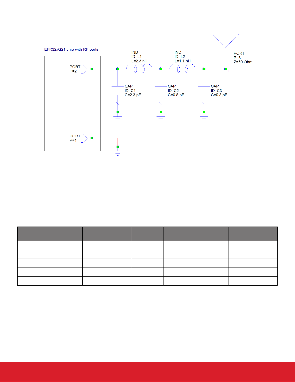
5.1.4 Recommended Matching Network for the +20 dBm PA
AN930.2: EFR32 Series 2 2.4 GHz Matching Guide
Recommended Matching Networks
Figure 5.4. Matching Network Schematic for the +20 dBm PA
It is recommended to use the matching network shown above when the maximum transmitting power requirement is +20 dBm (+10
dBm < TX power ≤ +20 dBm), i.e., the application utilizes the +20 dBm PA to achieve the possible highest TX power level available.
Due to the optimized power efficiency, the need for 5-element matching network here is mostly driven by the harmonic suppression
requirements. The unused RF2G4_IO pin can be grounded directly. Make a short from the pin back to the center exposed pad of the
part under the chip.
Table 5.4. Final SMD Values for the +20 dBm PA (5-element)
Schematic Reference Desig-
Component Value Tolerance Part Number Manufacturer
nator
C1 2.3 pF ± 0.05 pF GRM0335C1H2R3WA01D Murata
L1 2.3 nH ± 0.1 nH LQP03HQ2N3B02D Murata
C2 0.8 pF ± 0.05 pF GRM0335C1HR80WA01D Murata
L2 1.1 nH ± 0.05 nH LQP03HQ1N1W02D Murata
C3 0.3 pF ± 0.05 pF GRM0335C1HR30WA01D Murata
silabs.com | Building a more connected world. Rev. 0.6 | 15
Page 16
5.1.5 Measurement Results
Table 5.5. Measurement Results for Each Power Level (PA), Avg., Conducted
AN930.2: EFR32 Series 2 2.4 GHz Matching Guide
Recommended Matching Networks
Match PA RX Sensitiv-
ity [dBm]
TX Power
[dBm]
PA Current
[mA]
H2 max
[dBm]
H3 max
[dBm]
H4 max
[dBm]
H5 max
0 dBm 0 dBm -96.4 -0.3 4.3 -60.1 -64.2 -67.9 -60.9
+10 dBm +10 dBm -96.5 10.6 29.9 -47.7 -48.8 -48.0 -48.0
0 / 10 dBm 0 dBm -96.4 -0.4 4.3 -62.1 -68.8 -68.8 -68.8
0 / 10 dBm +10 dBm -96.4 10.4 29.9 -62.1 -49.5 -68.1 -45.5
+20 dBm +20 dBm -96.3 20.2 178.1 -55.4 -51.5 -52.1 -52.1
RX Sensitivity test conditions: 1Mbps BLE PHY (MSK), BER < 0.1%.
[dBm]
silabs.com | Building a more connected world. Rev. 0.6 | 16
Page 17

AN930.2: EFR32 Series 2 2.4 GHz Matching Guide
Recommended Matching Networks
5.2 EFR32xG22 Matching Networks
This section provides matching networks recommended for use with the EFR32xG22 with different layout approaches. It is important to
emphasize that the tuned matching component values strongly depend on the layout drawing and so it is recommended to follow the
layout guidelines as documented in AN928.2: EFR32 Series 2 Layout Design Guide.
There are two different layout concepts designed for EFR32xG22:
1. Existing layout concept: This layout approach utilizes a short GND trace connection between the first shunt matching capacitor and
RFVSS ground pin of the chip, and that first shunt matching capacitor is not connected to any via or component-layer GND pour
(except for the exposed chip pad through the RFVSS pin). The second shunt matching capacitor is grounded through a single via
to an inner layer's GND plane. Also, there is about 70 mils of total copper keep-out on the component-layer GND pour around the
RF matching circuit.
2. Generic layout concept: This layout concept follows more generic RF layout guidelines and no special or unique approach is applied. The shunt matching capacitors are connected to the component-layer GND pour with multiple stitching vias as well and there
is about 11 mils of copper keep-out between the matching components and the top layer's GND plane.
The EFR32xG22 data sheet provides a suggested matching network with the layout concept #1 with the existing layout approach. All
data sheet parameters are captured with this configuration. This solution provides excellent conducted RF performance, but it has two
drawbacks: it is only marginally able to transmit at the output power level of +8 dBm, and the radiated 5th harmonic can also be marginal in FCC certifications. To ensure margins on the radiated 5th harmonic, it is especially important to place the first shunt matching
capacitor very close to the chip pins and follow the reference radio board's PCB stack-up. Also, Silicon Labs reference radio boards are
available with the existing layout concept.
Silicon Labs recommends following the generic layout concept #2. This solution is more robust and has bigger margins on the radiated
harmonics, while +8 dBm TX output power can also be reached with some margin. The RF performance when following this layout
approach is not as sensitive to the PCB stack-up, component spreading, and layout parasitics as the existing layout concept.
silabs.com | Building a more connected world. Rev. 0.6 | 17
Page 18
AN930.2: EFR32 Series 2 2.4 GHz Matching Guide
Recommended Matching Networks
5.2.1 Data Sheet Matching Network Recommendation for Following the Existing Layout Concept #1
Figure 5.5. Matching Network Schematic Following Existing Layout Concept #1
Use the matching network shown above with EFR32xG22 for any achievable power level when following the existing layout concept #1.
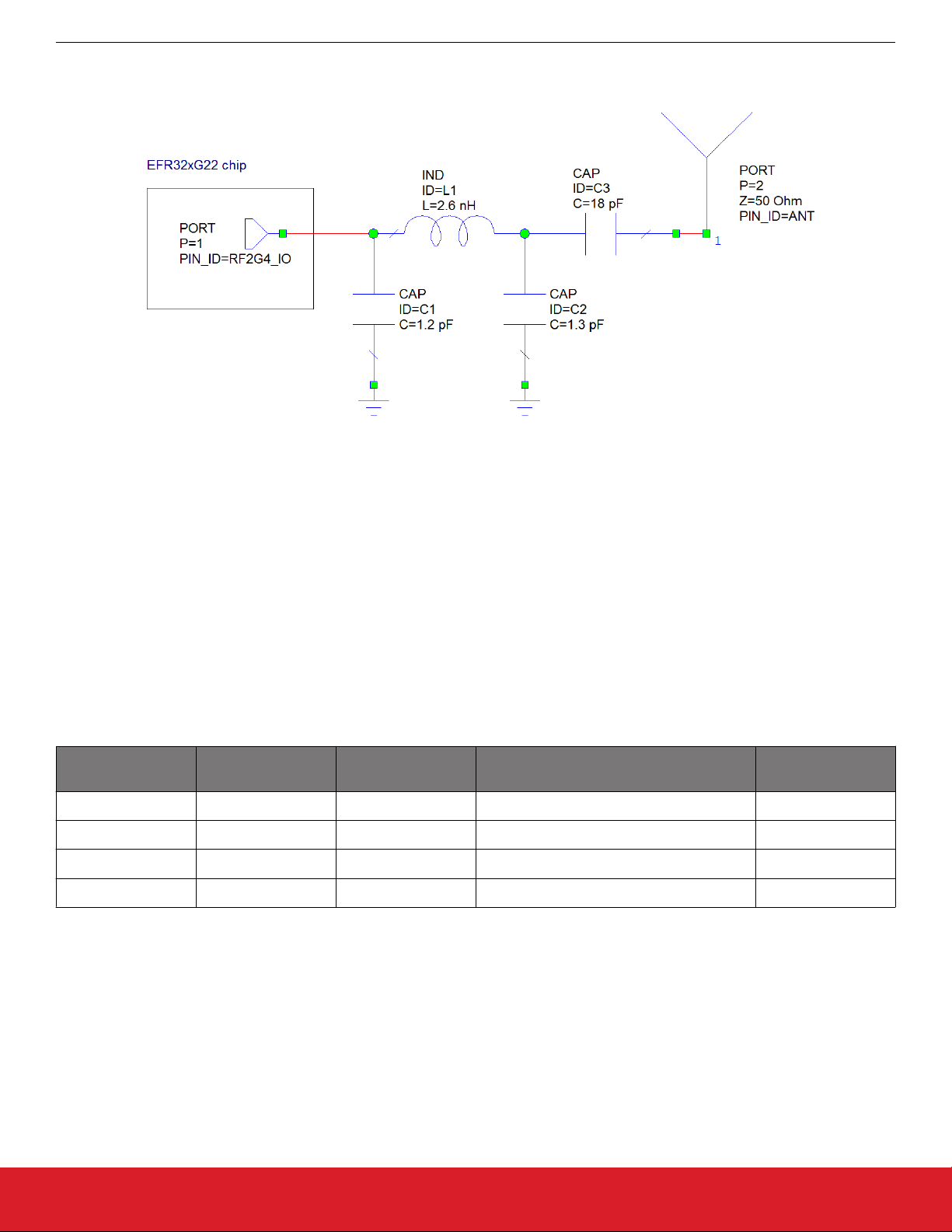
The series dc-blocking capacitor (C3) is mandatory when utilizing the 0 dBm PA, but the matching network shown above is optimized
for any power level equal or below +6 dBm, i.e., simultaneously optimized with the 0 and +6 dBm PA as well.
The matching network component values are optimized for a 4-layer PCB with a separation of 300 μm between the top (component
side) and first inner layer. These values can be used for a PCB with more layers as well, if the distance between the top (matching
circuit component side) and first inner layer is kept close to 300 μm.
Furthermore, the EFR32xG22 part is also capable of transmitting at the output power level up to +8 dBm. However, higher than +6 dBm
TX power output will result in higher current consumption and harmonic levels, and the +8 dBm TXP is not guaranteed over temperature and process variations. The power code for +8 dBm TXP needs to be maximized in RAIL using the matching network shown above
with the PCB stack-up mentioned. The recommended raw power setting in RAIL is 127. For different PCB stack-up configurations the
match might need tuning, and the slight tuning of the C1 component is the most effective to achieve different max power levels.
Table 5.6. Final SMD Values for the 0/6 dBm PA Match on a 4-layer PCB when Following the Existing Layout Concept
Schematic Refer-
Component Value Tolerance Part Number Manufacturer
ence Designator
C1 1.2 pF ± 0.05 pF GRM0335C1H1R2WA01D Murata
L1 2.6 nH ± 0.1 nH LQP03HQ2N6B02 Murata
C2 1.3 pF ± 0.1 pF GRM0335C1H1R3BA01D Murata
C3 18 pF ± 2 % GJM0335C1E180GB01D Murata
silabs.com | Building a more connected world. Rev. 0.6 | 18
Page 19

5.2.2 Recommended Matching Network for Following the Generic Layout Concept #2
Figure 5.6. Recommended Matching Network Schematic Following the Generic Layout Concept #2
AN930.2: EFR32 Series 2 2.4 GHz Matching Guide
Recommended Matching Networks
Use the matching network shown above with EFR32xG22 for any achievable power level on a 2- or more layer PCB where the gap
between the top and first inner layer (or bottom layer for 2-layer PCB) is a maximum of 800 µm while following the generic layout concept #2 discussed above. The series dc-blocking capacitor (C3) is mandatory when utilizing the 0 dBm PA, but the matching network
shown above is optimized for any power level equal or below +6 dBm. The matching network is simultaneously optimized for both the 0
and +6 dBm PA.
Furthermore, the EFR32xG22 part is also capable of transmitting at the output power level up to +8 dBm. However, higher than +6 dBm
TX power output will result in higher current consumption and harmonic levels, and the +8 dBm TXP is not guaranteed over temperature and process variations. The power code for +8 dBm TXP needs to be set close to the maximum in RAIL using the matching network shown above with the PCB stack-up described above. The recommended raw power setting in RAIL is 95.
The matching network component values are optimized for PCB stack-up configurations with a separation of maximum 800 μm (32
mils) between the top and first inner layer (or bottom layer for 2-layer PCB). Tested with the standard radio board stack-up with a 0.3
mm gap between the top and first inner layer, with a 4-layer PCB with 0.07 mm gap between the top and first inner layer, and with a 2layer 32 mils (0.8 mm) thick PCB.
Table 5.7. Final SMD Values for the 0 / 6 dBm PA Match when Following the Generic Layout Concept
Schematic Refer-
Component Value Tolerance Part Number Manufacturer
ence Designator
C1 1.7 pF ± 0.1 pF GRM0335C1H1R7BA01D Murata
L1 2.7 nH ± 0.1 nH LQP03TN2N7B02D Murata
C2 1.3 pF ± 0.1 pF GRM0335C1H1R3BA01D Murata
C3 18 pF ± 2 % GJM0335C1E180GB01D Murata
silabs.com | Building a more connected world. Rev. 0.6 | 19
Page 20
5.2.3 Measurement Results
Table 5.8. Measurement Results for Each Power Level (PA), Avg., Conducted
AN930.2: EFR32 Series 2 2.4 GHz Matching Guide
Recommended Matching Networks
Layout
Concept
PA PCB RX Sensi-
tivity
1
[dBm]
TX Power
[dBm]
Current
Cons. [mA]
H2 max
[dBm]
H3 max
[dBm]
Existing #1 0 dBm 4-layer -98.4 0.2 4.6 -57.1 -62.7
Existing #1 +6 dBm 4-layer -98.4
Generic #2 +6 dBm 4-layer -98.5
Generic #2 +6 dBm 4-layer -98.5
Generic #2 +6 dBm 2-layer -98.3
6.0
6.0
8.5
6.0
3
3
4
3
8.7 -52.0 -46.1 -66.5 -64.8
8.9 -54.9 -39.0
10.8 -53.3 -36.7 -65.5 -45.7
8.9 -65.0 -36.0 -56.0 -43.0
Generic #2 0 dBm 2-layer -98.3 -0.2 4.7 -53.2 -58.5
Note:
1. Test conditions: 1 Mbps BLE PHY (MSK), BER < 0.1%.
2. Under SA noise floor.
3. Tested at +6 dBm power level.
4. Tested at raw power level setting of 127.
H4 max
[dBm]
2
-70
2
-70
2
-70
H5 max
[dBm]
2
-70
-53.4
2
-70
silabs.com | Building a more connected world. Rev. 0.6 | 20
Page 21
AN930.2: EFR32 Series 2 2.4 GHz Matching Guide
Appendix 1 PA Optimum Termination Impedance on EFR32xG21
6. Appendix 1 PA Optimum Termination Impedance on EFR32xG21
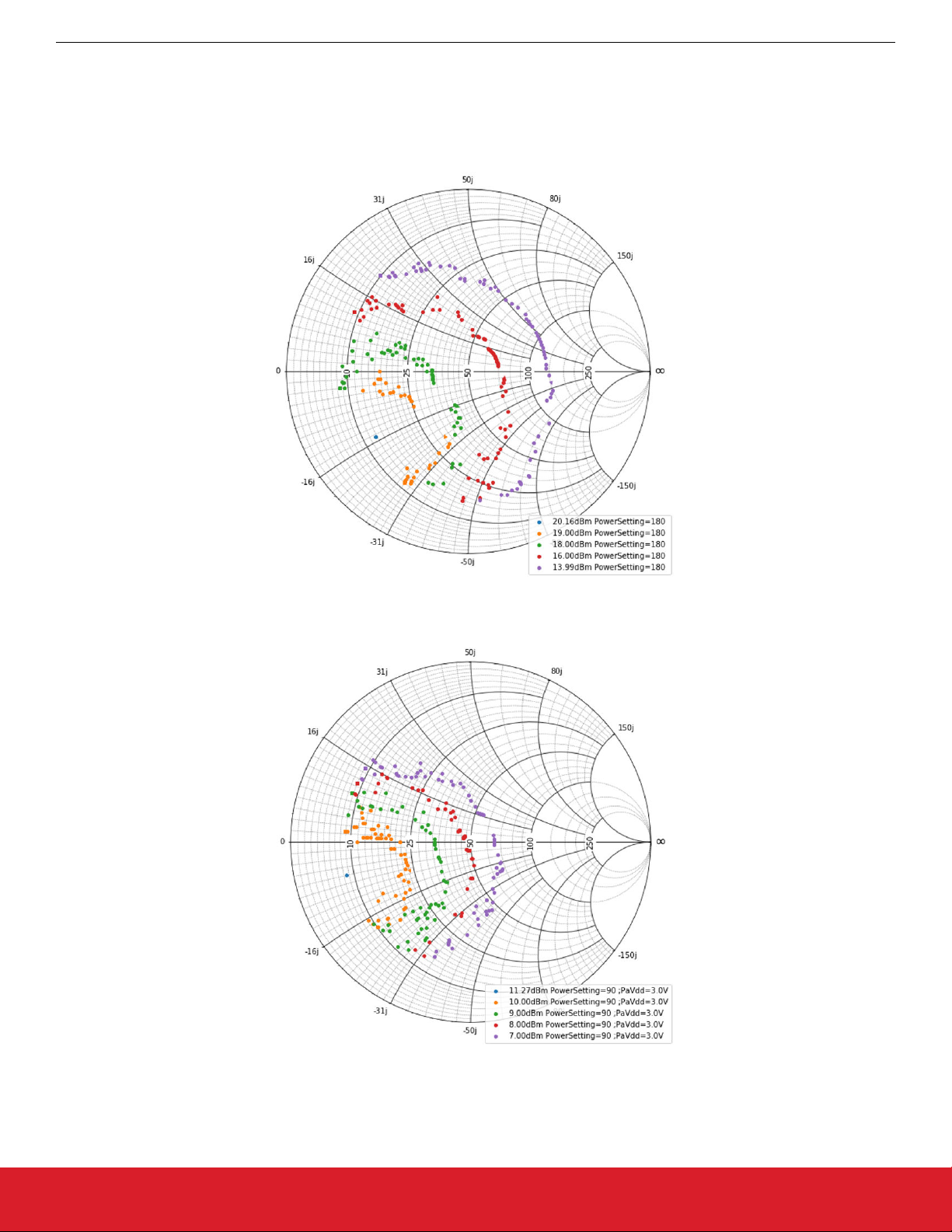
The matching network should present an optimum impedance for the PA at the RF2G4_IO pin for the best RF performance if a 50 Ω
termination is applied at the antenna port. The optimum impedance depends on the power level and is also different depending on
which internal PA is actively used. The optimum impedances are determined empirically by load-pull methods. The load-pull curves for
each PA are shown in the following figures below.
Figure 6.1. Load-pull curves for the 20 dBm PA
Figure 6.2. Load-pull curves for the 10 dBm PA
silabs.com | Building a more connected world. Rev. 0.6 | 21
Page 22

AN930.2: EFR32 Series 2 2.4 GHz Matching Guide
Appendix 1 PA Optimum Termination Impedance on EFR32xG21
Figure 6.3. Load-pull curves for the 0 dBm PA
silabs.com | Building a more connected world. Rev. 0.6 | 22
Page 23

AN930.2: EFR32 Series 2 2.4 GHz Matching Guide
Revision History
7. Revision History
Revision 0.6
February 2021
• Removed diversity applications language from sections 3.1 EFR32xG21 RF Front-End Overview and 4.1.1 EFR32xG21 Optimum
PA Load Impedance.
Revision 0.5
November 2020
• Updated EFR32xG22 generic recommended matching network
Revision 0.4
May 2020
• Added matching recommendation for EFR32xG22 on a 4-layer thin PCB with +8 dBm test data
Revision 0.3
March 2020
• Added content for EFR32xG22 part
Revision 0.2
November 2019
• Highlighting that 0 dBm PA requires to be DC-blocked
• Updating load-pull impedance data and adding load-pull impedance curves for each PA
• Adding discrete 4-element combined 0 / 10 dBm PA match
Revision 0.1
February 2019
Initial release.
silabs.com | Building a more connected world. Rev. 0.6 | 23
Page 24

Simplicity Studio
One-click access to MCU and wireless
tools, documentation, software, source
code libraries & more. Available for
Windows, Mac and Linux!
IoT Portfolio
www.silabs.com/IoT
Disclaimer
Silicon Labs intends to provide customers with the latest, accurate, and in-depth documentation of all peripherals and modules available for system and software implementers using or
intending to use the Silicon Labs products. Characterization data, available modules and peripherals, memory sizes and memory addresses refer to each specific device, and “Typical”
parameters provided can and do vary in different applications. Application examples described herein are for illustrative purposes only. Silicon Labs reserves the right to make changes
without further notice to the product information, specifications, and descriptions herein, and does not give warranties as to the accuracy or completeness of the included information.
Without prior notification, Silicon Labs may update product firmware during the manufacturing process for security or reliability reasons. Such changes will not alter the specifications or
the performance of the product. Silicon Labs shall have no liability for the consequences of use of the information supplied in this document. This document does not imply or expressly
grant any license to design or fabricate any integrated circuits. The products are not designed or authorized to be used within any FDA Class III devices, applications for which FDA
premarket approval is required, or Life Support Systems without the specific written consent of Silicon Labs. A “Life Support System” is any product or system intended to support or
sustain life and/or health, which, if it fails, can be reasonably expected to result in significant personal injury or death. Silicon Labs products are not designed or authorized for military
applications. Silicon Labs products shall under no circumstances be used in weapons of mass destruction including (but not limited to) nuclear, biological or chemical weapons, or
missiles capable of delivering such weapons. Silicon Labs disclaims all express and implied warranties and shall not be responsible or liable for any injuries or damages related to use of
a Silicon Labs product in such unauthorized applications.
Trademark Information
Silicon Laboratories Inc.®, Silicon Laboratories®, Silicon Labs®, SiLabs® and the Silicon Labs logo®, Bluegiga®, Bluegiga Logo®, ClockBuilder®, CMEMS®, DSPLL®, EFM®,
EFM32®, EFR, Ember®, Energy Micro, Energy Micro logo and combinations thereof, “the world’s most energy friendly microcontrollers”, Ember®, EZLink®, EZRadio®, EZRadioPRO®,
Gecko®, Gecko OS, Gecko OS Studio, ISOmodem®, Precision32®, ProSLIC®, Simplicity Studio®, SiPHY®, Telegesis, the Telegesis Logo®, USBXpress®, Zentri, the Zentri logo and
Zentri DMS, Z-Wave®, and others are trademarks or registered trademarks of Silicon Labs. ARM, CORTEX, Cortex-M3 and THUMB are trademarks or registered trademarks of ARM
Holdings. Keil is a registered trademark of ARM Limited. Wi-Fi is a registered trademark of the Wi-Fi Alliance. All other products or brand names mentioned herein are trademarks of
their respective holders.
Silicon Laboratories Inc.
400 West Cesar Chavez
Austin, TX 78701
USA
http: //www.silabs.com
SW/HW
ww.silabs.com/simplicity
w
Quality
ww.silabs.com/quality
w
Support & Community
abs.com/community
www.sil
 Loading...