

Page 1
EFM8 Sleepy Bee Family
EFM8SB2 Reference Manual
The EFM8SB2, part of the Sleepy Bee family of MCUs, is the
world’s most energy friendly 8-bit microcontrollers with a comprehensive feature set in small packages.
These devices offer lowest power consumption by combining innovative low energy techniques and short wakeup times from energy saving modes into small packages, making
them well-suited for any battery operated applications. With an efficient 8051 core, 6-bit
current reference, and precision analog, the EFM8SB2 family is also optimal for embedded applications.
EFM8SB2 applications include the following:
• Hand-held devices
Industrial controls
•
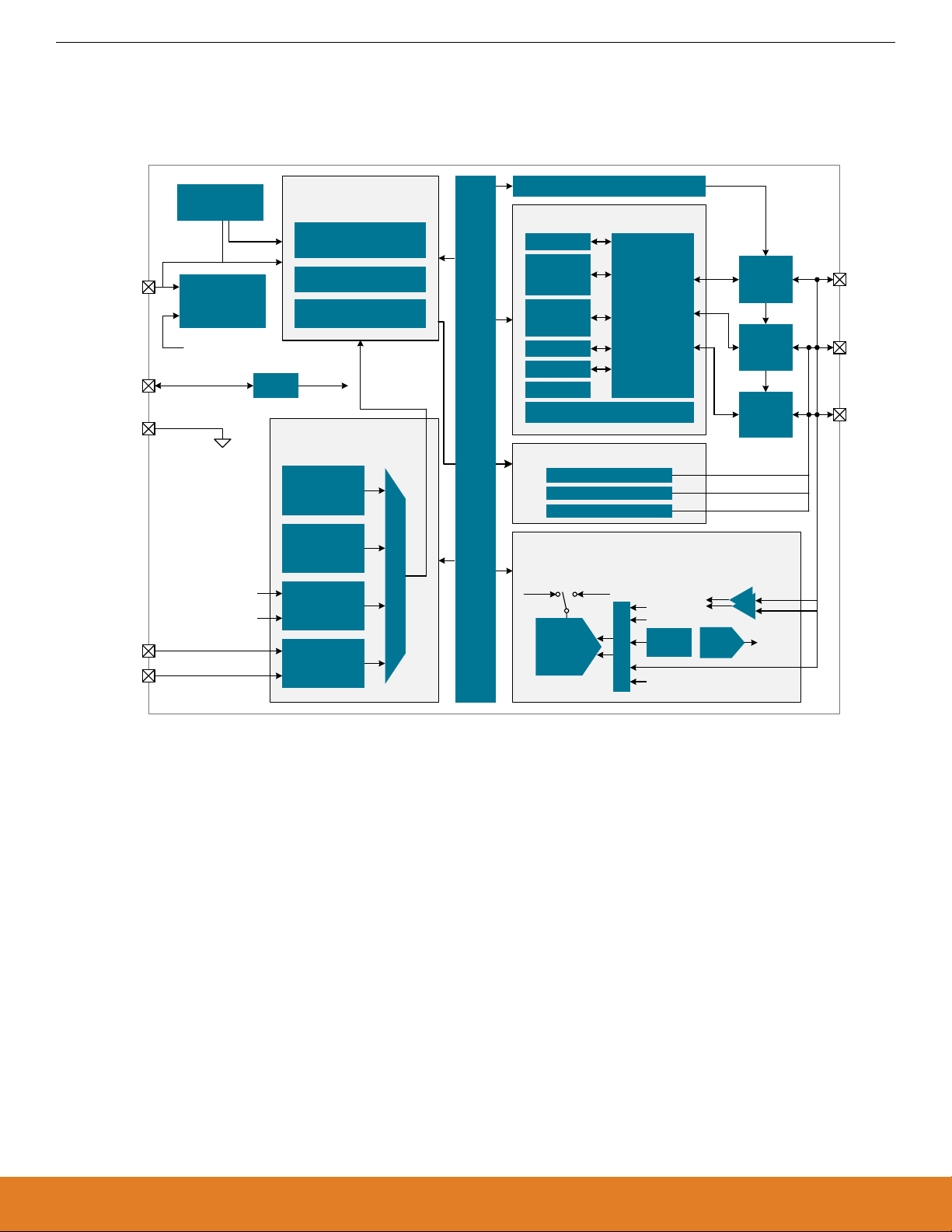
CIP-51 8051 Core
Flash Program
Memory
(up to 64 KB)
Core / Memory Clock Management
(25 MHz)
RAM Memory
(4352 bytes)
• Battery-operated consumer electronics
•
Sensor interfaces
External
Oscillator
Debug Interface
with C2
External 32 kHz
RTC Oscillator
Low Power 20
MHz RC
Oscillator
High Frequency
24.5 MHz RC
Oscillator
ENERGY FRIENDLY FEATURES
• Lowest MCU sleep current with supply
brownout detection (50 nA)
•
Lowest MCU active current with these
features (170 μA / MHz at 24.5 MHz clock
rate)
• Lowest MCU sleep current using internal
RTC operating and supply brownout
detection (<300 nA)
• Ultra-fast wake up for digital and analog
peripherals (< 2 μs)
• Integrated low drop out (LDO) voltage
regulator to maintain ultra-low active
current at all voltages
Energy Management
Internal LDO
Regulator
Brown-Out Detector
Power-On Reset
8-bit SFR bus
Serial Interfaces Timers and Triggers Analog Interfaces
UART
2
I
C / SMBus
Lowest power mode with peripheral operational:
silabs.com | Smart. Connected. Energy-friendly. Rev. 0.1
2 x SPI
IdleNormal Suspend Sleep
External
Interrupts
General
Purpose I/O
Pin Reset
Pin Wakeup
Timers
0/1/2/3
Watchdog
Timer
PCA/PWM
Real Time
Clock
ADC
Comparator 1
Internal Current Reference
Comparator 0
Internal Voltage
Reference
SecurityI/O Ports
16/32-bit CRC
Page 2
1. System Overview
1.1 Introduction
EFM8SB2 Reference Manual
System Overview
C2CK/RSTb
VDD
GND
XTAL3
XTAL4
Power On
Reset/PMU
Debug /
Programming
Hardware
C2D
Power Net
Analog
Power
Wake
Reset
XTAL1
XTAL2
CIP-51 8051 Controller
Core
64/32/16 KB ISP Flash
Program Memory
256 Byte SRAM
4096 Byte XRAM
VREG
Digital
Power
System Clock
Configuration
Precision
24.5 MHz
Oscillator
Low Power
20 MHz
Oscillator
External
Oscillator
Circuit
RTC
Oscillator
SYSCLK
SFR
Bus
Port I/O Configuration
Digital Peripherals
UART
Timers 0,
1, 2, 3
Priority
PCA/WDT
SMBus
SPI 0,1
CRC
Crossbar Control
Crossbar
Decoder
External Memory Interface
Control
Address
Data
Analog Peripherals
VREF
External
VREF
10-bit
300ksps
ADC
AMUX
VDD
VREF
Temp
Sensor
GND
Internal
Port 0
Drivers
Port 1
Drivers
Port 2
Drivers
Comparators
+
+
-
-
6-bit
IREF
P0.n
P1.n
P2.n
IREF0
Figure 1.1. Detailed EFM8SB2 Block Diagram
silabs.com | Smart. Connected. Energy-friendly. Rev. 0.1 | 1
Page 3

EFM8SB2 Reference Manual
System Overview
1.2 Power
internal circuitry draws power from the VDD supply pin. External I/O pins are powered from the VIO supply voltage (or VDD on devi-
All
ces without a separate VIO connection), while most of the internal circuitry is supplied by an on-chip LDO regulator. Control over the
device power can be achieved by enabling/disabling individual peripherals as needed. Each analog peripheral can be disabled when
not in use and placed in low power mode. Digital peripherals, such as timers and serial buses, have their clocks gated off and draw little
power when they are not in use.
Table 1.1. Power Modes
Power Mode Details Mode Entry Wake-Up Sources
Normal Core and all peripherals clocked and fully operational — —
Idle • Core halted
•
All peripherals clocked and fully operational
Set IDLE bit in PCON0 Any interrupt
• Code resumes execution on wake event
Suspend • Core and digital peripherals halted
•
Internal oscillators disabled
• Code resumes execution on wake event
1. Switch SYSCLK to
HFOSC0 or LPOSC0
2.
Set SUSPEND bit in
PMU0CF
• RTC0 Alarm Event
• RTC0 Fail Event
• Port Match Event
• Comparator 0 Rising
Edge
Sleep • Most internal power nets shut down
•
Select circuits remain powered
• Pins retain state
• All RAM and SFRs retain state
• Code resumes execution on wake event
1. Disable unused analog peripherals
2.
Set SLEEP bit in
PMU0CF
• RTC0 Alarm Event
• RTC0 Fail Event
• Port Match Event
• Comparator 0 Rising
Edge
1.3 I/O
Digital
and analog resources are externally available on the device’s multi-purpose I/O pins. Port pins P0.0-P2.6 can be defined as general-purpose I/O (GPIO), assigned to one of the internal digital resources through the crossbar or dedicated channels, or assigned to an
analog function. Port pin P2.7 can be used as GPIO. Additionally, the C2 Interface Data signal (C2D) is shared with P2.7.
• Up to 24 multi-functions I/O pins, supporting digital and analog functions.
• Flexible priority crossbar decoder for digital peripheral assignment.
• Two drive strength settings for each pin.
• Two direct-pin interrupt sources with dedicated interrupt vectors (INT0 and INT1).
• Up to 16 direct-pin interrupt sources with shared interrupt vector (Port Match).
1.4 Clocking
The CPU core and peripheral subsystem may be clocked by both internal and external oscillator resources. By default, the system
clock comes up running from the 20 MHz low power oscillator divided by 8.
• Provides clock to core and peripherals.
• 20 MHz low power oscillator (LPOSC0), accurate to +/- 10% over supply and temperature corners.
• 24.5 MHz internal oscillator (HFOSC0), accurate to +/- 2% over supply and temperature corners.
• External RTC 32 kHz crystal.
• External RC, C, CMOS, and high-frequency crystal clock options (EXTCLK).
• Clock divider with eight settings for flexible clock scaling: Divide the selected clock source by 1, 2, 4, 8, 16, 32, 64, or 128.
silabs.com | Smart. Connected. Energy-friendly. Rev. 0.1 | 2
Page 4

EFM8SB2 Reference Manual
System Overview
1.5 Counters/Timers and PWM
Real Time Clock (RTC0)
RTC is an ultra low power, 36 hour 32-bit independent time-keeping Real Time Clock with alarm. The RTC has a dedicated 32 kHz
The
oscillator. No external resistor or loading capacitors are required, and a missing clock detector features alerts the system if the external
crystal fails. The on-chip loading capacitors are programmable to 16 discrete levels allowing compatibility with a wide range of crystals.
The RTC module includes the following features:
• Up to 36 hours (32-bit) of independent time keeping.
• Support for external 32 kHz crystal or internal self-oscillate mode.
• Internal crystal loading capacitors with 16 levels.
• Operation in the lowest power mode and across the full supported voltage range.
• Alarm and oscillator failure events to wake from the lowest power mode or reset the device.
Programmable Counter Array (PCA0)
The programmable counter array (PCA) provides multiple channels of enhanced timer and PWM functionality while requiring less CPU
intervention than standard counter/timers. The PCA consists of a dedicated 16-bit counter/timer and one 16-bit capture/compare module for each channel. The counter/timer is driven by a programmable timebase that has flexible external and internal clocking options.
Each capture/compare module may be configured to operate independently in one of five modes: Edge-Triggered Capture, Software
Timer, High-Speed Output, Frequency Output, or Pulse-Width Modulated (PWM) Output. Each capture/compare module has its own
associated I/O line (CEXn) which is routed through the crossbar to port I/O when enabled.
• 16-bit time base.
• Programmable clock divisor and clock source selection.
• Up to six independently-configurable channels
• 8, 9, 10, 11 and 16-bit PWM modes (edge-aligned operation).
• Frequency output mode.
• Capture on rising, falling or any edge.
• Compare function for arbitrary waveform generation.
• Software timer (internal compare) mode.
• Integrated watchdog timer.
Timers (Timer 0, Timer 1, Timer 2, and Timer 3)
Several counter/timers are included in the device: two are 16-bit counter/timers compatible with those found in the standard 8051, and
the rest are 16-bit auto-reload timers for timing peripherals or for general purpose use. These timers can be used to measure time intervals, count external events and generate periodic interrupt requests. Timer 0 and Timer 1 are nearly identical and have four primary
modes of operation. The other timers offer both 16-bit and split 8-bit timer functionality with auto-reload and capture capabilities.
Timer 0 and Timer 1 include the following features:
• Standard 8051 timers, supporting backwards-compatibility with firmware and hardware.
• Clock sources include SYSCLK, SYSCLK divided by 12, 4, or 48, the External Clock divided by 8, or an external pin.
• 8-bit auto-reload counter/timer mode
• 13-bit counter/timer mode
• 16-bit counter/timer mode
• Dual 8-bit counter/timer mode (Timer 0)
Timer 2 and Timer 3 are 16-bit timers including the following features:
• Clock sources include SYSCLK, SYSCLK divided by 12, or the External Clock divided by 8.
• 16-bit auto-reload timer mode
• Dual 8-bit auto-reload timer mode
• Comparator 0 or RTC0 capture (Timer 2)
• Comparator 1 or EXTCLK/8 capture (Timer 3)
silabs.com | Smart. Connected. Energy-friendly. Rev. 0.1 | 3
Page 5

EFM8SB2 Reference Manual
System Overview
Watchdog Timer (WDT0)
device includes a programmable watchdog timer (WDT) integrated within the PCA0 peripheral. A WDT overflow forces the MCU
The
into the reset state. To prevent the reset, the WDT must be restarted by application software before overflow. If the system experiences
a software or hardware malfunction preventing the software from restarting the WDT, the WDT overflows and causes a reset. Following
a reset, the WDT is automatically enabled and running with the default maximum time interval. If needed, the WDT can be disabled by
system software. The state of the RSTb pin is unaffected by this reset.
The Watchdog Timer integrated in the PCA0 peripheral has the following features:
• Programmable timeout interval
• Runs from the selected PCA clock source
• Automatically enabled after any system reset
1.6 Communications and Other Digital Peripherals
Universal Asynchronous Receiver/Transmitter (UART0)
UART0 is an asynchronous, full duplex serial port offering modes 1 and 3 of the standard 8051 UART. Enhanced baud rate support
allows a wide range of clock sources to generate standard baud rates. Received data buffering allows UART0 to start reception of a
second incoming data byte before software has finished reading the previous data byte.
The UART module provides the following features:
• Asynchronous transmissions and receptions
• Baud rates up to SYSCLK/2 (transmit) or SYSCLK/8 (receive)
• 8- or 9-bit data
• Automatic start and stop generation
Serial Peripheral Interface (SPI0 and SPI1)
The serial peripheral interface (SPI) module provides access to a flexible, full-duplex synchronous serial bus. The SPI can operate as a
master or slave device in both 3-wire or 4-wire modes, and supports multiple masters and slaves on a single SPI bus. The slave-select
(NSS) signal can be configured as an input to select the SPI in slave mode, or to disable master mode operation in a multi-master
environment, avoiding contention on the SPI bus when more than one master attempts simultaneous data transfers. NSS can also be
configured as a firmware-controlled chip-select output in master mode, or disabled to reduce the number of pins required. Additional
general purpose port I/O pins can be used to select multiple slave devices in master mode.
The SPI module includes the following features:
• Supports 3- or 4-wire operation in master or slave modes.
• Supports external clock frequencies up to SYSCLK / 2 in master mode and SYSCLK / 10 in slave mode.
• Support for four clock phase and polarity options.
• 8-bit dedicated clock clock rate generator.
• Support for multiple masters on the same data lines.
System Management Bus / I2C (SMB0)
The SMBus I/O interface is a two-wire, bi-directional serial bus. The SMBus is compliant with the System Management Bus Specification, version 1.1, and compatible with the I2C serial bus.
The SMBus module includes the following features:
• Standard (up to 100 kbps) and Fast (400 kbps) transfer speeds.
• Support for master, slave, and multi-master modes.
• Hardware synchronization and arbitration for multi-master mode.
• Clock low extending (clock stretching) to interface with faster masters.
• Hardware support for 7-bit slave and general call address recognition.
• Firmware support for 10-bit slave address decoding.
• Ability to inhibit all slave states.
• Programmable data setup/hold times.
silabs.com | Smart. Connected. Energy-friendly. Rev. 0.1 | 4
Page 6

EFM8SB2 Reference Manual
System Overview
External Memory Interface (EMIF0)
External Memory Interface (EMIF) enables access of off-chip memories and memory-mapped devices connected to the GPIO
The
ports. The external memory space may be accessed using the external move instruction (MOVX) with the target address specified in
either 8-bit or 16-bit formats.
• Supports multiplexed memory access.
• Four external memory modes:
• Internal only.
• Split mode without bank select.
• Split mode with bank select.
• External only
• Configurable ALE (address latch enable) timing.
• Configurable address setup and hold times.
• Configurable write and read pulse widths.
16/32-bit CRC (CRC0)
The cyclic redundancy check (CRC) module performs a CRC using a 16-bit or 32-bit polynomial. CRC0 accepts a stream of 8-bit data
and posts the result to an internal register. In addition to using the CRC block for data manipulation, hardware can automatically CRC
the flash contents of the device.
The CRC module is designed to provide hardware calculations for flash memory verification and communications protocols. The CRC
module includes the following features:
• Support for CCITT-16 polynomial (0x1021).
• Support for CRC-32 polynomial (0x04C11DB7).
• Byte-level bit reversal.
• Automatic CRC of flash contents on one or more 1024-byte blocks.
• Initial seed selection of 0x0000/0x00000000 or 0xFFFF/0xFFFFFFFF.
1.7 Analog
Programmable Current Reference (IREF0)
The programmable current reference (IREF0) module enables current source or sink with two output current settings: Low Power Mode
and High Current Mode. The maximum current output in Low Power Mode is 63 µA (1 µA steps) and the maximum current output in
High Current Mode is 504 µA (8 µA steps).
The IREF module includes the following features:
• Capable of sourcing or sinking current in programmable steps.
• Two operational modes: Low Power Mode and High Current Mode.
silabs.com | Smart. Connected. Energy-friendly. Rev. 0.1 | 5
Page 7

EFM8SB2 Reference Manual
System Overview
10-Bit Analog-to-Digital Converter (ADC0)
ADC is a successive-approximation-register (SAR) ADC with 10- and 8-bit modes, integrated track-and hold and a programmable
The
window detector. The ADC is fully configurable under software control via several registers. The ADC may be configured to measure
different signals using the analog multiplexer. The voltage reference for the ADC is selectable between internal and external reference
sources.
• Up to 22 external inputs.
• Single-ended 10-bit mode.
• Supports an output update rate of 300 ksps samples per second.
• Operation in low power modes at lower conversion speeds.
• Asynchronous hardware conversion trigger, selectable between software, external I/O and internal timer sources.
• Output data window comparator allows automatic range checking.
• Support for burst mode, which produces one set of accumulated data per conversion-start trigger with programmable power-on settling and tracking time.
• Conversion complete and window compare interrupts supported.
• Flexible output data formatting.
• Includes an internal 1.65 V fast-settling reference and support for external reference.
• Integrated temperature sensor.
Low Current Comparators (CMP0, CMP1)
Analog comparators are used to compare the voltage of two analog inputs, with a digital output indicating which input voltage is higher.
External input connections to device I/O pins and internal connections are available through separate multiplexers on the positive and
negative inputs. Hysteresis, response time, and current consumption may be programmed to suit the specific needs of the application.
The comparator module includes the following features:
• Up to 12 external positive inputs.
• Up to 11 external negative inputs.
• Additional input options:
• Capacitive Sense Comparator output.
• VDD.
• VDD divided by 2.
• Internal connection to LDO output.
• Direct connection to GND.
• Synchronous and asynchronous outputs can be routed to pins via crossbar.
• Programmable hysteresis between 0 and +/-20 mV.
• Programmable response time.
• Interrupts generated on rising, falling, or both edges.
silabs.com | Smart. Connected. Energy-friendly. Rev. 0.1 | 6
Page 8

EFM8SB2 Reference Manual
System Overview
1.8 Reset Sources
Reset circuitry allows the controller to be easily placed in a predefined default condition. On entry to this reset state, the following occur:
The core halts program execution.
•
• Module registers are initialized to their defined reset values unless the bits reset only with a power-on reset.
• External port pins are forced to a known state.
• Interrupts and timers are disabled.
All registers are reset to the predefined values noted in the register descriptions unless the bits only reset with a power-on reset. The
contents of RAM are unaffected during a reset; any previously stored data is preserved as long as power is not lost. The Port I/O latches are reset to 1 in open-drain mode. Weak pullups are enabled during and after the reset. For Supply Monitor and power-on resets,
the RSTb pin is driven low until the device exits the reset state. On exit from the reset state, the program counter (PC) is reset, and the
system clock defaults to an internal oscillator. The Watchdog Timer is enabled, and program execution begins at location 0x0000.
Reset sources on the device include the following:
• Power-on reset
• External reset pin
• Comparator reset
• Software-triggered reset
• Supply monitor reset (monitors VDD supply)
• Watchdog timer reset
• Missing clock detector reset
• Flash error reset
• RTC0 alarm or oscillator failure
1.9 Debugging
The EFM8SB2 devices include an on-chip Silicon Labs 2-Wire (C2) debug interface to allow flash programming and in-system debugging with the production part installed in the end application. The C2 interface uses a clock signal (C2CK) and a bi-directional C2 data
signal (C2D) to transfer information between the device and a host system. See the C2 Interface Specification for details on the C2
protocol.
1.10 Bootloader
All devices come pre-programmed with a UART bootloader. This bootloader resides in flash and can be erased if it is not needed.
silabs.com | Smart. Connected. Energy-friendly. Rev. 0.1 | 7
Page 9

EFM8SB2 Reference Manual
Memory Organization
2. Memory Organization
2.1 Memory Organization
The memory organization of the CIP-51 System Controller is similar to that of a standard 8051. There are two separate memory
spaces: program memory and data memory. Program and data memory share the same address space but are accessed via different
instruction types. Program memory consists of a non-volatile storage area that may be used for either program code or non-volatile
data storage. The data memory, consisting of "internal" and "external" data space, is implemented as RAM, and may be used only for
data storage. Program execution is not supported from the data memory space.
2.2 Program Memory
The CIP-51 core has a 64 KB program memory space. The product family implements some of this program memory space as in-system, re-programmable flash memory. Flash security is implemented by a user-programmable location in the flash block and provides
read, write, and erase protection. All addresses not specified in the device memory map are reserved and may not be used for code or
data storage.
MOVX Instruction and Program Memory
The MOVX instruction in an 8051 device is typically used to access external data memory. On the devices, the MOVX instruction is
normally used to read and write on-chip XRAM, but can be re-configured to write and erase on-chip flash memory space. MOVC instructions are always used to read flash memory, while MOVX write instructions are used to erase and write flash. This flash access
feature provides a mechanism for the product to update program code and use the program memory space for non-volatile data storage.
2.3 Data Memory
The RAM space on the chip includes both an "internal" RAM area which is accessed with MOV instructions, and an on-chip "external"
RAM area which is accessed using MOVX instructions. Total RAM varies, based on the specific device. The device memory map has
more details about the specific amount of RAM available in each area for the different device variants.
Internal RAM
There are 256 bytes of internal RAM mapped into the data memory space from 0x00 through 0xFF. The lower 128 bytes of data memory are used for general purpose registers and scratch pad memory. Either direct or indirect addressing may be used to access the lower
128 bytes of data memory. Locations 0x00 through 0x1F are addressable as four banks of general purpose registers, each bank consisting of eight byte-wide registers. The next 16 bytes, locations 0x20 through 0x2F, may either be addressed as bytes or as 128 bit
locations accessible with the direct addressing mode.
The upper 128 bytes of data memory are accessible only by indirect addressing. This region occupies the same address space as the
Special Function Registers (SFR) but is physically separate from the SFR space. The addressing mode used by an instruction when
accessing locations above 0x7F determines whether the CPU accesses the upper 128 bytes of data memory space or the SFRs. Instructions that use direct addressing will access the SFR space. Instructions using indirect addressing above 0x7F access the upper
128 bytes of data memory.
General Purpose Registers
The lower 32 bytes of data memory, locations 0x00 through 0x1F, may be addressed as four banks of general-purpose registers. Each
bank consists of eight byte-wide registers designated R0 through R7. Only one of these banks may be enabled at a time. Two bits in
the program status word (PSW) register, RS0 and RS1, select the active register bank. This allows fast context switching when entering
subroutines and interrupt service routines. Indirect addressing modes use registers R0 and R1 as index registers.
silabs.com | Smart. Connected. Energy-friendly. Rev. 0.1 | 8
Page 10

EFM8SB2 Reference Manual
Memory Organization
Bit Addressable Locations
addition to direct access to data memory organized as bytes, the sixteen data memory locations at 0x20 through 0x2F are also ac-
In
cessible as 128 individually addressable bits. Each bit has a bit address from 0x00 to 0x7F. Bit 0 of the byte at 0x20 has bit address
0x00 while bit 7 of the byte at 0x20 has bit address 0x07. Bit 7 of the byte at 0x2F has bit address 0x7F. A bit access is distinguished
from a full byte access by the type of instruction used (bit source or destination operands as opposed to a byte source or destination).
The MCS-51™ assembly language allows an alternate notation for bit addressing of the form XX.B where XX is the byte address and B
is the bit position within the byte. For example, the instruction:
Mov C, 22.3h
moves the Boolean value at 0x13 (bit 3 of the byte at location 0x22) into the Carry flag.
Stack
A
programmer's stack can be located anywhere in the 256-byte data memory. The stack area is designated using the Stack Pointer
(SP) SFR. The SP will point to the last location used. The next value pushed on the stack is placed at SP+1 and then SP is incremented. A reset initializes the stack pointer to location 0x07. Therefore, the first value pushed on the stack is placed at location 0x08, which
is also the first register (R0) of register bank 1. Thus, if more than one register bank is to be used, the SP should be initialized to a
location in the data memory not being used for data storage. The stack depth can extend up to 256 bytes.
External RAM
On devices with more than 256 bytes of on-chip RAM, the additional RAM is mapped into the external data memory space (XRAM).
Addresses in XRAM area accessed using the external move (MOVX) instructions.
Note: The 16-bit MOVX write instruction is also used for writing and erasing the flash memory. More details may be found in the flash
memory section.
silabs.com | Smart. Connected. Energy-friendly. Rev. 0.1 | 9
Page 11

2.4 Memory Map
EFM8SB2 Reference Manual
Memory Organization
0xFFFF
Reserved
0xFBFF Lock Byte
0xFBFE
Security Page
1024 Bytes
0xF800
0x0000
63 KB Flash
(63 x 1024 Byte pages)
0x03FF
0x0000
Figure 2.1. Flash Memory Map — 64 KB Devices
Scratchpad
1024 Bytes
silabs.com | Smart. Connected. Energy-friendly. Rev. 0.1 | 10
Page 12

0xFFFF
Reserved
0x7FFF Lock Byte
0x7FFE
Security Page
1024 Bytes
0x7C00
EFM8SB2 Reference Manual
Memory Organization
0x0000
32 KB Flash
(32 x 1024 Byte pages)
0x03FF
0x0000
Figure 2.2. Flash Memory Map — 32 KB Devices
Scratchpad
1024 Bytes
silabs.com | Smart. Connected. Energy-friendly. Rev. 0.1 | 11
Page 13

0xFFFF
Reserved
0x3FFF Lock Byte
0x3FFE
Security Page
1024 Bytes
0x3C00
EFM8SB2 Reference Manual
Memory Organization
0x0000
16 KB Flash
(16 x 1024 Byte pages)
0x03FF
0x0000
Figure 2.3. Flash Memory Map — 16 KB Devices
On-Chip RAM
Accessed with MOV Instructions as Indicated
0xFF
Upper 128 Bytes
RAM
(Indirect Access)
Special Function
Registers
(Direct Access)
0x80
0x7F
Lower 128 Bytes RAM
(Direct or Indirect Access)
0x30
0x2F
0x20
0x1F
0x00
General-Purpose Register Banks
Bit-Addressable
Scratchpad
1024 Bytes
Figure 2.4. Direct / Indirect RAM Memory
silabs.com | Smart. Connected. Energy-friendly. Rev. 0.1 | 12
Page 14

0xFFFF
0x1000
0x0FFF
0x0000
EFM8SB2 Reference Manual
Memory Organization
On-Chip XRAM
Accessed with MOVX Instructions
Shadow XRAM
Duplicates 0x0000-0x0FFF
On 4096 B boundaries
XRAM
4096 Bytes
Figure 2.5. XRAM Memory
silabs.com | Smart. Connected. Energy-friendly. Rev. 0.1 | 13
Page 15

EFM8SB2 Reference Manual
Special Function Registers
3. Special Function Registers
3.1 Special Function Register Access
The direct-access data memory locations from 0x80 to 0xFF constitute the special function registers (SFRs). The SFRs provide control
and data exchange with the CIP-51's resources and peripherals. The CIP-51 duplicates the SFRs found in a typical 8051 implementation as well as implementing additional SFRs used to configure and access the sub-systems unique to the MCU. This allows the addi-
tion of new functionality while retaining compatibility with the MCS-51 ™ instruction set.
The SFR registers are accessed anytime the direct addressing mode is used to access memory locations from 0x80 to 0xFF. SFRs
with addresses ending in 0x0 or 0x8 (e.g., P0, TCON, SCON0, IE, etc.) are bit-addressable as well as byte-addressable. All other SFRs
are byte-addressable only. Unoccupied addresses in the SFR space are reserved for future use. Accessing these areas will have an
indeterminate effect and should be avoided.
SFR Paging
The CIP-51 features SFR paging, allowing the device to map many SFRs into the 0x80 to 0xFF memory address space. The SFR
memory space has 256 pages. In this way, each memory location from 0x80 to 0xFF can access up to 256 SFRs. The EFM8SB2
devices utilize multiple SFR pages. All of the common 8051 SFRs are available on all pages. Certain SFRs are only available on a
subset of pages. SFR pages are selected using the SFRPAGE register. The procedure for reading and writing an SFR is as follows:
1. Select the appropriate SFR page using the SFRPAGE register.
2. Use direct accessing mode to read or write the special function register (MOV instruction).
The SFRPAGE register only needs to be changed in the case that the SFR to be accessed does not exist on the currently-selected
page. See the SFR memory map for details on the locations of each SFR. It is good practice inside of interrupt service routines to save
the current SFRPAGE at the beginning of the ISR and restore this value at the end.
Interrupts and SFR Paging
In any system which changes the SFRPAGE while interrupts are active, it is good practice to save the current SFRPAGE value upon
ISR entry, and then restore the SFRPAGE before exiting the ISR. This ensures that SFRPAGE will remain at the desired setting when
returning from the ISR.
silabs.com | Smart. Connected. Energy-friendly. Rev. 0.1 | 14
Page 16

EFM8SB2 Reference Manual
Special Function Registers
3.2 Special Function Register Memory Map
Table 3.1. Special Function Registers by Address
Address SFR Page Address SFR Page
(*bit-addressable) 0x00 0x0F (*bit-addressable) 0x00 0x0F
0x80* P0 0xC0* SMB0CN0 -
0x81 SP 0xC1 SMB0CF -
0x82 DPL 0xC2 SMB0DAT -
0x83 DPH 0xC3 ADC0GTL -
0x84 SPI1CFG - 0xC4 ADC0GTH -
0x85 SPI1CKR TOFFL 0xC5 ADC0LTL -
0x86 SPI1DAT TOFFH 0xC6 ADC0LTH -
0x87 PCON0 0xC7 P0MASK -
0x88* TCON - 0xC8* TMR2CN0 -
0x89 TMOD - 0xC9 REG0CN -
0x8A TL0 - 0xCA TMR2RLL -
0x8B TL1 - 0xCB TMR2RLH -
0x8C TH0 - 0xCC TMR2L -
0x8D TH1 - 0xCD TMR2H -
0x8E CKCON0 - 0xCE PCA0CPM5 -
0x8F PSCTL - 0xCF P1MAT -
0x90* P1 0xD0* PSW
0x91 TMR3CN0 CRC0DAT 0xD1 REF0CN -
0x92 TMR3RLL CRC0CN0 0xD2 PCA0CPL5 -
0x93 TMR3RLH CRC0IN 0xD3 PCA0CPH5 -
0x94 TMR3L - 0xD4 P0SKIP -
0x95 TMR3H CRC0FLIP 0xD5 P1SKIP -
0x96 - CRC0AUTO 0xD6 P2SKIP -
0x97 - CRC0CNT 0xD7 P0MAT -
0x98* SCON0 - 0xD8* PCA0CN0 -
0x99 SBUF0 - 0xD9 PCA0MD -
0x9A CMP1CN0 - 0xDA PCA0CPM0 -
0x9B CMP0CN0 - 0xDB PCA0CPM1 -
0x9C CMP1MD - 0xDC PCA0CPM2 -
0x9D CMP0MD - 0xDD PCA0CPM3 -
0x9E CMP1MX - 0xDE PCA0CPM4 -
0x9F CMP0MX - 0xDF PCA0PWM -
0xA0* P2 0xE0* ACC
silabs.com | Smart. Connected. Energy-friendly. Rev. 0.1 | 15
Page 17

EFM8SB2 Reference Manual
Special Function Registers
Address SFR Page Address SFR Page
(*bit-addressable) 0x00 0x0F (*bit-addressable) 0x00 0x0F
0xA1 SPI0CFG - 0xE1 XBR0 -
0xA2 SPI0CKR - 0xE2 XBR1 -
0xA3 SPI0DAT - 0xE3 XBR2 -
0xA4 P0MDOUT P0DRV 0xE4 IT01CF -
0xA5 P1MDOUT P1DRV 0xE5 -
0xA6 P2MDOUT P2DRV 0xE6 EIE1
0xA7 SFRPAGE 0xE7 EIE2
0xA8* IE 0xE8* ADC0CN0 -
0xA9 CLKSEL 0xE9 PCA0CPL1 -
0xAA EMI0CN - 0xEA PCA0CPH1 -
0xAB EMI0CF - 0xEB PCA0CPL2 -
0xAC RTC0ADR - 0xEC PCA0CPH2 -
0xAD RTC0DAT - 0xED PCA0CPL3 -
0xAE RTC0KEY - 0xEE PCA0CPH3 -
0xAF EMI0TC - 0xEF RSTSRC -
0xB0* SPI1CN0 - 0xF0* B
0xB1 XOSC0CN - 0xF1 P0MDIN -
0xB2 HFO0CN - 0xF2 P1MDIN -
0xB3 HFO0CAL - 0xF3 P2MDIN -
0xB4 - 0xF4 SMB0ADR -
0xB5 PMU0CF - 0xF5 SMB0ADM -
0xB6 FLSCL - 0xF6 EIP1
0xB7 FLKEY - 0xF7 EIP2
0xB8* IP 0xF8* SPI0CN0 -
0xB9 IREF0CN0 - 0xF9 PCA0L -
0xBA ADC0AC ADC0PWR 0xFA PCA0H -
0xBB ADC0MX - 0xFB PCA0CPL0 -
0xBC ADC0CF - 0xFC PCA0CPH0 -
0xBD ADC0L ADC0TK 0xFD PCA0CPL4 -
0xBE ADC0H - 0xFE PCA0CPH4 -
0xBF P1MASK - 0xFF VDM0CN -
Table 3.2. Special Function Registers by Name
Register Address SFR Pages Description
ACC 0xE0 ALL Accumulator
ADC0AC 0xBA 0x00 ADC0 Accumulator Configuration
silabs.com | Smart. Connected. Energy-friendly. Rev. 0.1 | 16
Page 18

Register Address SFR Pages Description
ADC0CF 0xBC 0x00 ADC0 Configuration
ADC0CN0 0xE8 0x00 ADC0 Control 0
ADC0GTH 0xC4 0x00 ADC0 Greater-Than High Byte
ADC0GTL 0xC3 0x00 ADC0 Greater-Than Low Byte
ADC0H 0xBE 0x00 ADC0 Data Word High Byte
ADC0L 0xBD 0x00 ADC0 Data Word Low Byte
ADC0LTH 0xC6 0x00 ADC0 Less-Than High Byte
ADC0LTL 0xC5 0x00 ADC0 Less-Than Low Byte
ADC0MX 0xBB 0x00 ADC0 Multiplexer Selection
ADC0PWR 0xBA 0x0F ADC0 Power Control
ADC0TK 0xBD 0x0F ADC0 Burst Mode Track Time
B 0xF0 ALL B Register
CKCON0 0x8E 0x00 Clock Control 0
EFM8SB2 Reference Manual
Special Function Registers
CLKSEL 0xA9 ALL Clock Select
CMP0CN0 0x9B 0x00 Comparator 0 Control 0
CMP0MD 0x9D 0x00 Comparator 0 Mode
CMP0MX 0x9F 0x00 Comparator 0 Multiplexer Selection
CMP1CN0 0x9A 0x00 Comparator 1 Control 0
CMP1MD 0x9C 0x00 Comparator 1 Mode
CMP1MX 0x9E 0x00 Comparator 1 Multiplexer Selection
CRC0AUTO 0x96 0x0F CRC0 Automatic Control
CRC0CN0 0x92 0x0F CRC0 Control 0
CRC0CNT 0x97 0x0F CRC0 Automatic Flash Sector Count
CRC0DAT 0x91 0x0F CRC0 Data Output
CRC0FLIP 0x95 0x0F CRC0 Bit Flip
CRC0IN 0x93 0x0F CRC0 Data Input
DPH 0x83 ALL Data Pointer High
DPL 0x82 ALL Data Pointer Low
EIE1 0xE6 ALL Extended Interrupt Enable 1
EIE2 0xE7 ALL Extended Interrupt Enable 2
EIP1 0xF6 ALL Extended Interrupt Priority 1
EIP2 0xF7 ALL Extended Interrupt Priority 2
EMI0CF 0xAB 0x00 External Memory Configuration
EMI0CN 0xAA 0x00 External Memory Interface Control
EMI0TC 0xAF 0x00 External Memory Timing Control
FLKEY 0xB7 0x00 Flash Lock and Key
FLSCL 0xB6 0x00 Flash Scale
silabs.com | Smart. Connected. Energy-friendly. Rev. 0.1 | 17
Page 19

Register Address SFR Pages Description
HFO0CAL 0xB3 0x00 High Frequency Oscillator Calibration
HFO0CN 0xB2 0x00 High Frequency Oscillator Control
IE 0xA8 ALL Interrupt Enable
IP 0xB8 ALL Interrupt Priority
IREF0CN0 0xB9 0x00 Current Reference Control 0
IT01CF 0xE4 0x00 INT0/INT1 Configuration
P0 0x80 ALL Port 0 Pin Latch
P0DRV 0xA4 0x0F Port 0 Drive Strength
P0MASK 0xC7 0x00 Port 0 Mask
P0MAT 0xD7 0x00 Port 0 Match
P0MDIN 0xF1 0x00 Port 0 Input Mode
P0MDOUT 0xA4 0x00 Port 0 Output Mode
P0SKIP 0xD4 0x00 Port 0 Skip
EFM8SB2 Reference Manual
Special Function Registers
P1 0x90 ALL Port 1 Pin Latch
P1DRV 0xA5 0x0F Port 1 Drive Strength
P1MASK 0xBF 0x00 Port 1 Mask
P1MAT 0xCF 0x00 Port 1 Match
P1MDIN 0xF2 0x00 Port 1 Input Mode
P1MDOUT 0xA5 0x00 Port 1 Output Mode
P1SKIP 0xD5 0x00 Port 1 Skip
P2 0xA0 ALL Port 2 Pin Latch
P2DRV 0xA6 0x0F Port 2 Drive Strength
P2MDIN 0xF3 0x00 Port 2 Input Mode
P2MDOUT 0xA6 0x00 Port 2 Output Mode
P2SKIP 0xD6 0x00 Port 2 Skip
PCA0CN0 0xD8 0x00 PCA Control 0
PCA0CPH0 0xFC 0x00 PCA Channel 0 Capture Module High Byte
PCA0CPH1 0xEA 0x00 PCA Channel 1 Capture Module High Byte
PCA0CPH2 0xEC 0x00 PCA Channel 2 Capture Module High Byte
PCA0CPH3 0xEE 0x00 PCA Channel 3 Capture Module High Byte
PCA0CPH4 0xFE 0x00 PCA Channel 4 Capture Module High Byte
PCA0CPH5 0xD3 0x00 PCA Channel 5 Capture Module High Byte
PCA0CPL0 0xFB 0x00 PCA Channel 0 Capture Module Low Byte
PCA0CPL1 0xE9 0x00 PCA Channel 1 Capture Module Low Byte
PCA0CPL2 0xEB 0x00 PCA Channel 2 Capture Module Low Byte
PCA0CPL3 0xED 0x00 PCA Channel 3 Capture Module Low Byte
PCA0CPL4 0xFD 0x00 PCA Channel 4 Capture Module Low Byte
silabs.com | Smart. Connected. Energy-friendly. Rev. 0.1 | 18
Page 20

Special Function Registers
Register Address SFR Pages Description
PCA0CPL5 0xD2 0x00 PCA Channel 5 Capture Module Low Byte
PCA0CPM0 0xDA 0x00 PCA Channel 0 Capture/Compare Mode
PCA0CPM1 0xDB 0x00 PCA Channel 1 Capture/Compare Mode
PCA0CPM2 0xDC 0x00 PCA Channel 2 Capture/Compare Mode
PCA0CPM3 0xDD 0x00 PCA Channel 3 Capture/Compare Mode
PCA0CPM4 0xDE 0x00 PCA Channel 4 Capture/Compare Mode
PCA0CPM5 0xCE 0x00 PCA Channel 5 Capture/Compare Mode
PCA0H 0xFA 0x00 PCA Counter/Timer High Byte
PCA0L 0xF9 0x00 PCA Counter/Timer Low Byte
PCA0MD 0xD9 0x00 PCA Mode
PCA0PWM 0xDF 0x00 PCA PWM Configuration
PCON0 0x87 ALL Power Control 0
PMU0CF 0xB5 0x00 Power Management Unit Configuration
EFM8SB2 Reference Manual
PSCTL 0x8F 0x00 Program Store Control
PSW 0xD0 ALL Program Status Word
REF0CN 0xD1 0x00 Voltage Reference Control
REG0CN 0xC9 0x00 Voltage Regulator Control
RSTSRC 0xEF 0x00 Reset Source
RTC0ADR 0xAC 0x00 RTC Address
RTC0DAT 0xAD 0x00 RTC Data
RTC0KEY 0xAE 0x00 RTC Lock and Key
SBUF0 0x99 0x00 UART0 Serial Port Data Buffer
SCON0 0x98 0x00 UART0 Serial Port Control
SFRPAGE 0xA7 ALL SFR Page
SMB0ADM 0xF5 0x00 SMBus 0 Slave Address Mask
SMB0ADR 0xF4 0x00 SMBus 0 Slave Address
SMB0CF 0xC1 0x00 SMBus 0 Configuration
SMB0CN0 0xC0 0x00 SMBus 0 Control
SMB0DAT 0xC2 0x00 SMBus 0 Data
SP 0x81 ALL Stack Pointer
SPI0CFG 0xA1 0x00 SPI0 Configuration
SPI0CKR 0xA2 0x00 SPI0 Clock Rate
SPI0CN0 0xF8 0x00 SPI0 Control
SPI0DAT 0xA3 0x00 SPI0 Data
SPI1CFG 0x84 0x00 SPI1 Configuration
SPI1CKR 0x85 0x00 SPI1 Clock Rate
SPI1CN0 0xB0 0x00 SPI1 Control
silabs.com | Smart. Connected. Energy-friendly. Rev. 0.1 | 19
Page 21

Register Address SFR Pages Description
SPI1DAT 0x86 0x00 SPI1 Data
TCON 0x88 0x00 Timer 0/1 Control
TH0 0x8C 0x00 Timer 0 High Byte
TH1 0x8D 0x00 Timer 1 High Byte
TL0 0x8A 0x00 Timer 0 Low Byte
TL1 0x8B 0x00 Timer 1 Low Byte
TMOD 0x89 0x00 Timer 0/1 Mode
TMR2CN0 0xC8 0x00 Timer 2 Control 0
TMR2H 0xCD 0x00 Timer 2 High Byte
TMR2L 0xCC 0x00 Timer 2 Low Byte
TMR2RLH 0xCB 0x00 Timer 2 Reload High Byte
TMR2RLL 0xCA 0x00 Timer 2 Reload Low Byte
TMR3CN0 0x91 0x00 Timer 3 Control 0
EFM8SB2 Reference Manual
Special Function Registers
TMR3H 0x95 0x00 Timer 3 High Byte
TMR3L 0x94 0x00 Timer 3 Low Byte
TMR3RLH 0x93 0x00 Timer 3 Reload High Byte
TMR3RLL 0x92 0x00 Timer 3 Reload Low Byte
TOFFH 0x86 0x0F Temperature Sensor Offset High
TOFFL 0x85 0x0F Temperature Sensor Offset Low
VDM0CN 0xFF 0x00 VDD Supply Monitor Control
XBR0 0xE1 0x00 Port I/O Crossbar 0
XBR1 0xE2 0x00 Port I/O Crossbar 1
XBR2 0xE3 0x00 Port I/O Crossbar 2
XOSC0CN 0xB1 0x00 External Oscillator Control
3.3 SFR Access Control Registers
3.3.1 SFRPAGE: SFR Page
Bit 7 6 5 4 3 2 1 0
Name SFRPAGE
Access RW
Reset 0x00
SFR Page = ALL; SFR Address: 0xA7
Bit Name Reset Access Description
7:0 SFRPAGE 0x00 RW SFR Page.
Specifies the SFR Page used when reading, writing, or modifying special function registers.
silabs.com | Smart. Connected. Energy-friendly. Rev. 0.1 | 20
Page 22

EFM8SB2 Reference Manual
Flash Memory
4. Flash Memory
4.1 Introduction
On-chip, re-programmable flash memory is included for program code and non-volatile data storage. The flash memory is organized in
1024-byte pages. It can be erased and written through the C2 interface or from firmware by overloading the MOVX instruction. Any
individual byte in flash memory must only be written once between page erase operations.
0xFFFF
Reserved
0xFBFF Lock Byte
0xFBFE
Security Page
1024 Bytes
0xF800
0x0000
63 KB Flash
(63 x 1024 Byte pages)
0x03FF
0x0000
Figure 4.1. Flash Memory Map — 64 KB Devices
Scratchpad
1024 Bytes
silabs.com | Smart. Connected. Energy-friendly. Rev. 0.1 | 21
Page 23

0xFFFF
Reserved
0x7FFF Lock Byte
0x7FFE
Security Page
1024 Bytes
0x7C00
EFM8SB2 Reference Manual
Flash Memory
0x0000
32 KB Flash
(32 x 1024 Byte pages)
0x03FF
0x0000
Figure 4.2. Flash Memory Map — 32 KB Devices
Scratchpad
1024 Bytes
silabs.com | Smart. Connected. Energy-friendly. Rev. 0.1 | 22
Page 24

0xFFFF
Reserved
0x3FFF Lock Byte
0x3FFE
Security Page
1024 Bytes
0x3C00
EFM8SB2 Reference Manual
Flash Memory
16 KB Flash
(16 x 1024 Byte pages)
0x0000
Figure 4.3. Flash Memory Map — 16 KB Devices
4.2 Features
The flash memory has the following features:
Up to 64 KB organized in 1024-byte sectors.
•
• In-system programmable from user firmware.
• Security lock to prevent unwanted read/write/erase access.
• 1024 bytes of non-volatile data storage in the Scratchpad.
0x03FF
0x0000
Scratchpad
1024 Bytes
silabs.com | Smart. Connected. Energy-friendly. Rev. 0.1 | 23
Page 25

EFM8SB2 Reference Manual
Flash Memory
4.3 Functional Description
4.3.1 Security Options
CIP-51 provides security options to protect the flash memory from inadvertent modification by software as well as to prevent the
The
viewing of proprietary program code and constants. The Program Store Write Enable (bit PSWE in register PSCTL) and the Program
Store Erase Enable (bit PSEE in register PSCTL) bits protect the flash memory from accidental modification by software. PSWE must
be explicitly set to 1 before software can modify the flash memory; both PSWE and PSEE must be set to 1 before software can erase
flash memory. Additional security features prevent proprietary program code and data constants from being read or altered across the
C2 interface.
A Security Lock Byte located in flash user space offers protection of the flash program memory from access (reads, writes, or erases)
by unprotected code or the C2 interface. See the specific device memory map for the location of the security byte. The flash security
mechanism allows the user to lock "n" flash pages, starting at page 0, where "n" is the 1s complement number represented by the
Security Lock Byte.
Note: The page containing the flash Security Lock Byte is unlocked when no other flash pages are locked (all bits of the Lock Byte are
1) and locked when any other flash pages are locked (any bit of the Lock Byte is 0).
Table 4.1. Security Byte Decoding
Security Lock Byte 111111101b
1s Complement 00000010b
Flash Pages Locked 3 (First two flash pages + Lock Byte Page)
The level of flash security depends on the flash access method. The three flash access methods that can be restricted are reads,
writes,
and erases from the C2 debug interface, user firmware executing on unlocked pages, and user firmware executing on locked
pages.
Table 4.2. Flash Security Summary—Firmware Permissions
Permissions according to the area firmware is executing from:
Target Area for Read / Write / Erase Unlocked User
Page
Locked User Page Unlocked Data
Page
Locked Data Page
Any Unlocked Page [R] [W] [E] [R] [W] [E] [R] [W] [E] [R] [W] [E]
Locked Page (except security page) reset [R] [W] [E] reset [R] [W] [E]
Locked Security Page reset [R] [W] reset [R] [W]
Reserved Area reset reset reset reset
[R] = Read permitted
[W] = Write permitted
[E] = Erase permitted
reset = Flash error reset triggered
n/a = Not applicable
Table 4.3. Flash Security Summary—C2 Permissions
Target Area for Read / Write / Erase Permissions from C2 interface
Any Unlocked Page [R] [W] [E]
Any Locked Page Device Erase Only
Reserved Area None
silabs.com | Smart. Connected. Energy-friendly. Rev. 0.1 | 24
Page 26

EFM8SB2 Reference Manual
Flash Memory
Target Area for Read / Write / Erase Permissions from C2 interface
[R] = Read permitted
[W] = Write permitted
[E] = Erase permitted
Device Erase Only = No read, write, or individual page erase is allowed. Must erase entire flash space.
None = Read, write and erase are not permitted
4.3.2 Programming the Flash Memory
Writes
to flash memory clear bits from logic 1 to logic 0 and can be performed on single byte locations. Flash erasures set bits back to
logic 1 and occur only on full pages. The write and erase operations are automatically timed by hardware for proper execution; data
polling to determine the end of the write/erase operation is not required. Code execution is stalled during a flash write/erase operation.
The simplest means of programming the flash memory is through the C2 interface using programming tools provided by Silicon Labs or
a third party vendor. Firmware may also be loaded into the device to implement code-loader functions or allow non-volatile data storage. To ensure the integrity of flash contents, it is strongly recommended that the on-chip supply monitor be enabled in any system that
includes code that writes and/or erases flash memory from software.
4.3.2.1 Flash Lock and Key Functions
Flash writes and erases by user software are protected with a lock and key function. The FLKEY register must be written with the correct key codes, in sequence, before flash operations may be performed. The key codes are 0xA5 and 0xF1. The timing does not matter, but the codes must be written in order. If the key codes are written out of order or the wrong codes are written, flash writes and
erases will be disabled until the next system reset. Flash writes and erases will also be disabled if a flash write or erase is attempted
before the key codes have been written properly. The flash lock resets after each write or erase; the key codes must be written again
before another flash write or erase operation can be performed.
4.3.2.2 Flash Page Erase Procedure
The flash memory is erased one page at a time by firmware using the MOVX write instruction with the address targeted to any byte
within the page. Before erasing a page of flash memory, flash write and erase operations must be enabled by setting the PSWE and
PSEE bits in the PSCTL register to logic 1 (this directs the MOVX writes to target flash memory and enables page erasure) and writing
the flash key codes in sequence to the FLKEY register. The PSWE and PSEE bits remain set until cleared by firmware.
Erase operation applies to an entire page (setting all bytes in the page to 0xFF). To erase an entire page, perform the following steps:
1. Disable interrupts (recommended).
2. Write the first key code to FLKEY: 0xA5.
3. Write the second key code to FLKEY: 0xF1.
4. Set the PSEE bit (register PSCTL).
5. Set the PSWE bit (register PSCTL).
6. Using the MOVX instruction, write a data byte to any location within the page to be erased.
7. Clear the PSWE and PSEE bits.
4.3.2.3 Flash Byte Write Procedure
The flash memory is written by firmware using the MOVX write instruction with the address and data byte to be programmed provided
as normal operands in DPTR and A. Before writing to flash memory using MOVX, flash write operations must be enabled by setting the
PSWE bit in the PSCTL register to logic 1 (this directs the MOVX writes to target flash memory) and writing the flash key codes in
sequence to the FLKEY register. The PSWE bit remains set until cleared by firmware. A write to flash memory can clear bits to logic 0
but cannot set them. A byte location to be programmed should be erased (already set to 0xFF) before a new value is written.
To write a byte of flash, perform the following steps:
1. Disable interrupts (recommended).
2. Write the first key code to FLKEY: 0xA5.
3. Write the second key code to FLKEY: 0xF1.
4. Set the PSWE bit (register PSCTL).
5. Clear the PSEE bit (register PSCTL).
6. Using the MOVX instruction, write a single data byte to the desired location within the desired page.
silabs.com | Smart. Connected. Energy-friendly. Rev. 0.1 | 25
Page 27

EFM8SB2 Reference Manual
Flash Memory
7. Clear the PSWE bit.
4.3.3 Flash Write and Erase Precautions
system which contains routines which write or erase flash memory from software involves some risk that the write or erase routines
Any
will execute unintentionally if the CPU is operating outside its specified operating range of supply voltage, system clock frequency or
temperature. This accidental execution of flash modifying code can result in alteration of flash memory contents causing a system failure that is only recoverable by re-flashing the code in the device.
To help prevent the accidental modification of flash by firmware, hardware restricts flash writes and erasures when the supply monitor is
not active and selected as a reset source. As the monitor is enabled and selected as a reset source by default, it is recommended that
systems writing or erasing flash simply maintain the default state.
The following sections provide general guidelines for any system which contains routines which write or erase flash from code. Additional flash recommendations and example code can be found in AN201: Writing to Flash From Firmware, available from the Silicon
Laboratories website.
Voltage Supply Maintenance and the Supply Monitor
• If the system power supply is subject to voltage or current "spikes," add sufficient transient protection devices to the power supply to
ensure that the supply voltages listed in the Absolute Maximum Ratings table are not exceeded.
• Make certain that the minimum supply rise time specification is met. If the system cannot meet this rise time specification, then add
an external supply brownout circuit to the RSTb pin of the device that holds the device in reset until the voltage supply reaches the
lower limit, and re-asserts RSTb if the supply drops below the low supply limit.
• Do not disable the supply monitor. If the supply monitor must be disabled in the system, firmware should be added to the startup
routine to enable the on-chip supply monitor and enable the supply monitor as a reset source as early in code as possible. This
should be the first set of instructions executed after the reset vector. For C-based systems, this may involve modifying the startup
code added by the C compiler. See your compiler documentation for more details. Make certain that there are no delays in software
between enabling the supply monitor and enabling the supply monitor as a reset source.
Note: The supply monitor must be enabled and enabled as a reset source when writing or erasing flash memory. A flash error reset
will occur if either condition is not met.
• As an added precaution if the supply monitor is ever disabled, explicitly enable the supply monitor and enable the supply monitor as
a reset source inside the functions that write and erase flash memory. The supply monitor enable instructions should be placed just
after the instruction to set PSWE to a 1, but before the flash write or erase operation instruction.
• Make certain that all writes to the RSTSRC (Reset Sources) register use direct assignment operators and explicitly do not use the
bit-wise operators (such as AND or OR). For example, "RSTSRC = 0x02" is correct. "RSTSRC |= 0x02" is incorrect.
• Make certain that all writes to the RSTSRC register explicitly set the PORSF bit to a 1. Areas to check are initialization code which
enables other reset sources, such as the Missing Clock Detector or Comparator, for example, and instructions which force a Software Reset. A global search on "RSTSRC" can quickly verify this.
PSWE Maintenance
• Reduce the number of places in code where the PSWE bit (in register PSCTL) is set to a 1. There should be exactly one routine in
code that sets PSWE to a 1 to write flash bytes and one routine in code that sets PSWE and PSEE both to a 1 to erase flash pages.
• Minimize the number of variable accesses while PSWE is set to a 1. Handle pointer address updates and loop variable maintenance
outside the "PSWE = 1;... PSWE = 0;" area.
• Disable interrupts prior to setting PSWE to a 1 and leave them disabled until after PSWE has been reset to 0. Any interrupts posted
during the flash write or erase operation will be serviced in priority order after the flash operation has been completed and interrupts
have been re-enabled by software.
• Make certain that the flash write and erase pointer variables are not located in XRAM. See your compiler documentation for instructions regarding how to explicitly locate variables in different memory areas.
• Add address bounds checking to the routines that write or erase flash memory to ensure that a routine called with an illegal address
does not result in modification of the flash.
System Clock
• If operating from an external crystal-based source, be advised that crystal performance is susceptible to electrical interference and is
sensitive to layout and to changes in temperature. If the system is operating in an electrically noisy environment, use the internal
oscillator or use an external CMOS clock.
• If operating from the external oscillator, switch to the internal oscillator during flash write or erase operations. The external oscillator
can continue to run, and the CPU can switch back to the external oscillator after the flash operation has completed.
silabs.com | Smart. Connected. Energy-friendly. Rev. 0.1 | 26
Page 28

EFM8SB2 Reference Manual
Flash Memory
4.3.4 Minimizing Flash Read Current
The flash memory is responsible for a substantial portion of the total digital supply current when the device is executing code. Below are
suggestions to minimize flash read current.
Use low power modes while waiting for an interrupt, rather than polling the interrupt flag.
1.
2. Disable the one-shot timer.
3. Reduce the number of toggling address lines for short code loops.
Using Low Power Modes
To reduce flash read current, use idle, suspend, or sleep modes while waiting for an interrupt, rather than polling the interrupt flag. Idle
mode is particularly well-suited for use in implementing short pauses, since the wake-up time is no more than three system clock cycles. See the Power Management chapter for details on the various low-power operating modes.
Disabling the One-Shot Timer
The flash has a one-shot timer that saves power when operating at system clock frequencies of 10 MHz or less. The one-shot timer
generates a minimum-duration enable signal for the flash sense amps on each clock cycle in which the flash memory is accessed. This
allows the flash to remain in a low power state for the remainder of the long clock cycle.
At clock frequencies above 10 MHz, the system clock cycle becomes short enough that the one-shot timer no longer provides a power
benefit. Disabling the one-shot timer at higher frequencies reduces power consumption. The one-shot is enabled by default, and it can
be disabled (bypassed) by setting the BYPASS bit in the FLSCL register. To reenable the one-shot, clear the BYPASS bit to logic 0.
Reduce Toggling Lines in Loops
Flash read current depends on the number of address lines that toggle between sequential flash read operations. In most cases, the
difference in power is relatively small (on the order of 5%).
The flash memory is organized in rows of 128 bytes. A substantial current increase can be detected when the read address jumps from
one row in the flash memory to another. Consider a 3-cycle loop (e.g., SJMP $, or while(1);) which straddles a flash row boundary. The
flash address jumps from one row to another on two of every three clock cycles. This can result in a current increase of up 30% when
compared to the same 3-cycle loop contained entirely within a single row.
To minimize the power consumption of small loops, it is best to locate them within a single row, if possible. To check if a loop is contained within a flash row, divide the starting address of the first instruction in the loop by 128. If the remainder (result of modulo operation) plus the length of the loop is less than 127, then the loop fits inside a single flash row. Otherwise, the loop will be straddling two
adjacent flash rows. If a loop executes in 20 or more clock cycles, then the transitions from one row to another will occur on relatively
few clock cycles, and any resulting increase in operating current will be negligible.
4.3.5 Scratchpad
An additional scratchpad area is available for non-volatile data storage. It is accessible at addresses 0x0000 to 0x03FF when the SFLE
bit is set to 1. The scratchpad area cannot be used for code execution. The scratchpad is locked when all other flash pages are locked,
and it is erased when a Flash Device Erase command is performed.
silabs.com | Smart. Connected. Energy-friendly. Rev. 0.1 | 27
Page 29

EFM8SB2 Reference Manual
Flash Memory
4.4 Flash Control Registers
4.4.1 PSCTL: Program Store Control
Bit 7 6 5 4 3 2 1 0
Name Reserved SFLE PSEE PSWE
Access R RW RW RW
Reset 0x00 0 0 0
SFR Page = 0x0; SFR Address: 0x8F
Bit Name Reset Access Description
7:3 Reserved Must write reset value.
2 SFLE 0 RW Scratchpad Flash Memory Access Enable.
When this bit is set, flash MOVC reads and MOVX writes from user software are directed to the Scratchpad flash sector.
Flash accesses outside the address range 0x0000-0x01FF should not be attempted and may yield undefined results when
SFLE is set to 1.
Value Name Description
0 SCRATCHPAD_DISA-
Flash access from user software directed to the Program/Data Flash sector.
BLED
1 SCRATCHPAD_ENA-
Flash access from user software directed to the Scratchpad sector.
BLED
1 PSEE 0 RW Program Store Erase Enable.
Setting this bit (in combination with PSWE) allows an entire page of flash program memory to be erased. If this bit is logic 1
and
flash writes are enabled (PSWE is logic 1), a write to flash memory using the MOVX instruction will erase the entire
page that contains the location addressed by the MOVX instruction. The value of the data byte written does not matter.
Value Name Description
0 ERASE_DISABLED Flash program memory erasure disabled.
1 ERASE_ENABLED Flash program memory erasure enabled.
0 PSWE 0 RW Program Store Write Enable.
Setting this bit allows writing a byte of data to the flash program memory using the MOVX write instruction. The flash location should be erased before writing data.
Value Name Description
0 WRITE_DISABLED Writes to flash program memory disabled.
1 WRITE_ENABLED Writes to flash program memory enabled; the MOVX write instruction targets flash
memory.
silabs.com | Smart. Connected. Energy-friendly. Rev. 0.1 | 28
Page 30

EFM8SB2 Reference Manual
Flash Memory
4.4.2 FLKEY: Flash Lock and Key
Bit 7 6 5 4 3 2 1 0
Name FLKEY
Access RW
Reset 0x00
SFR Page = 0x0; SFR Address: 0xB7
Bit Name Reset Access Description
7:0 FLKEY 0x00 RW Flash Lock and Key Register.
Write:
This
register provides a lock and key function for flash erasures and writes. Flash writes and erases are enabled by writing
0xA5 followed by 0xF1 to the FLKEY register. Flash writes and erases are automatically disabled after the next write or
erase is complete. If any writes to FLKEY are performed incorrectly, or if a flash write or erase operation is attempted while
these operations are disabled, the flash will be permanently locked from writes or erasures until the next device reset. If an
application never writes to flash, it can intentionally lock the flash by writing a non-0xA5 value to FLKEY from firmware.
Read:
When read, bits 1-0 indicate the current flash lock state.
00: Flash is write/erase locked.
01: The first key code has been written (0xA5).
10: Flash is unlocked (writes/erases allowed).
11: Flash writes/erases are disabled until the next reset.
4.4.3 FLSCL: Flash Scale
Bit 7 6 5 4 3 2 1 0
Name Reserved BYPASS Reserved
Access R RW R
Reset 0 0 0x00
SFR Page = 0x0; SFR Address: 0xB6
Bit Name Reset Access Description
7 Reserved Must write reset value.
6 BYPASS 0 RW Flash Read Timing One-Shot Bypass.
Value Name Description
0 ONE_SHOT The one-shot determines the flash read time. This setting should be used for op-
erating frequencies less than 14 MHz.
1 SYSCLK The system clock determines the flash read time. This setting should be used for
frequencies greater than 14 MHz.
5:0 Reserved Must write reset value.
When changing the BYPASS bit from 1 to 0, the third opcode byte fetched from program memory is indeterminate. Therefore, the
operation which clears the BYPASS bit should be immediately followed by a benign 3-byte instruction whose third byte is a don't care.
An
example of such an instruction is a 3-byte MOV that targets the CRC0FLIP register. When programming in C, the dummy value
written to CRC0FLIP should be a non-zero value to prevent the compiler from generating a 2-byte MOV instruction.
silabs.com | Smart. Connected. Energy-friendly. Rev. 0.1 | 29
Page 31

EFM8SB2 Reference Manual
Device Identification
5. Device Identification
5.1 Unique Identifier
A 32-bit unique identifier (UID) is pre-loaded upon device reset into the last four bytes of the XRAM area on all devices. The UID can be
read by firmware using MOVX instructions and through the debug port.
As the UID appears in RAM, firmware can overwrite the UID during normal operation. The bytes in memory will be automatically reinitialized with the UID value after any device reset. Firmware using this area of memory should always initialize the memory to a known
value, as any previous data stored at these locations will be overwritten and not retained through a reset.
Table 5.1. UID Location in Memory
Device XRAM Addresses
EFM8SB20F64G
EFM8SB20F32G
(MSB) 0x0FFF, 0x0FFE, 0x0FFD, 0x0FFC (LSB)
silabs.com | Smart. Connected. Energy-friendly. Rev. 0.1 | 30
Page 32

EFM8SB2 Reference Manual
Interrupts
6. Interrupts
6.1 Introduction
The MCU core includes an extended interrupt system supporting multiple interrupt sources and priority levels. The allocation of interrupt
sources between on-chip peripherals and external input pins varies according to the specific version of the device.
Interrupt sources may have one or more associated interrupt-pending flag(s) located in an SFR local to the associated peripheral.
When a peripheral or external source meets a valid interrupt condition, the associated interrupt-pending flag is set to logic 1.
If interrupts are enabled for the source, an interrupt request is generated when the interrupt-pending flag is set. As soon as execution of
the current instruction is complete, the CPU generates an LCALL to a predetermined address to begin execution of an interrupt service
routine (ISR). Each ISR must end with an RETI instruction, which returns program execution to the next instruction that would have
been executed if the interrupt request had not occurred. If interrupts are not enabled, the interrupt-pending flag is ignored by the hardware and program execution continues as normal. The interrupt-pending flag is set to logic 1 regardless of whether the interrupt is enabled.
Each interrupt source can be individually enabled or disabled through the use of an associated interrupt enable bit in the IE and EIEn
registers. However, interrupts must first be globally enabled by setting the EA bit to logic 1 before the individual interrupt enables are
recognized. Setting the EA bit to logic 0 disables all interrupt sources regardless of the individual interrupt-enable settings.
Some interrupt-pending flags are automatically cleared by the hardware when the CPU vectors to the ISR or by other hardware conditions. However, most are not cleared by the hardware and must be cleared by software before returning from the ISR. If an interruptpending flag remains set after the CPU completes the return-from-interrupt (RETI) instruction, a new interrupt request will be generated
immediately and the CPU will re-enter the ISR after the completion of the next instruction.
6.2 Interrupt Sources and Vectors
The CIP51 core supports interrupt sources for each peripheral on the device. Software can simulate an interrupt for many peripherals
by setting any interrupt-pending flag to logic 1. If interrupts are enabled for the flag, an interrupt request will be generated and the CPU
will vector to the ISR address associated with the interrupt-pending flag. Refer to the data sheet section associated with a particular onchip peripheral for information regarding valid interrupt conditions for the peripheral and the behavior of its interrupt-pending flag(s).
6.2.1 Interrupt Priorities
Each interrupt source can be individually programmed to one of two priority levels: low or high. A low priority interrupt service routine
can be preempted by a high priority interrupt. A high priority interrupt cannot be preempted. Each interrupt has an associated interrupt
priority bit in the IP and EIPn registers, which are used to configure its priority level. Low priority is the default. If two interrupts are
recognized simultaneously, the interrupt with the higher priority is serviced first. If both interrupts have the same priority level, a fixed
order is used to arbitrate, based on the interrupt source's location in the interrupt vector table. Interrupts with a lower number in the
vector table have priority.
6.2.2 Interrupt Latency
Interrupt response time depends on the state of the CPU when the interrupt occurs. Pending interrupts are sampled and priority decoded on every system clock cycle. Therefore, the fastest possible response time is 5 system clock cycles: 1 clock cycle to detect the
interrupt and 4 clock cycles to complete the LCALL to the ISR. If an interrupt is pending when a RETI is executed, a single instruction is
executed before an LCALL is made to service the pending interrupt. Therefore, the maximum response time for an interrupt (when no
other interrupt is currently being serviced or the new interrupt is of greater priority) occurs when the CPU is performing an RETI instruction followed by a DIV as the next instruction. In this case, the response time is 18 system clock cycles: 1 clock cycle to detect the
interrupt, 5 clock cycles to execute the RETI, 8 clock cycles to complete the DIV instruction and 4 clock cycles to execute the LCALL to
the ISR. If the CPU is executing an ISR for an interrupt with equal or higher priority, the new interrupt will not be serviced until the
current ISR completes, including the RETI and following instruction. If more than one interrupt is pending when the CPU exits an ISR,
the CPU will service the next highest priority interrupt that is pending.
silabs.com | Smart. Connected. Energy-friendly. Rev. 0.1 | 31
Page 33

EFM8SB2 Reference Manual
6.2.3 Interrupt Summary
Table 6.1. Interrupt Priority Table
Interrupt Source Vector Priority Primary Enable Auxiliary Enable(s) Pending Flag(s)
Reset 0x0000 Top - - -
External Interrupt 0 0x0003 0 IE_EX0 - TCON_IE0
Timer 0 Overflow 0x000B 1 IE_ET0 - TCON_TF0
External Interrupt 1 0x0013 2 IE_EX1 - TCON_IE1
Timer 1 Overflow 0x001B 3 IE_ET1 - TCON_TF1
UART 0 0x0023 4 IE_ES0 - SCON0_RI
SCON0_TI
Interrupts
Timer 2 Overflow 0x002B 5 IE_ET2 TMR2CN0_TF2CEN
TMR2CN0_TF2LEN
TMR2CN0_TF2H
TMR2CN0_TF2L
SPI0 0x0033 6 IE_ESPI0 - SPI0CN0_MODF
SPI0CN0_RXOVRN
SPI0CN0_SPIF
SPI0CN0_WCOL
SMBus 0 0x003B 7 EIE1_ESMB0 - SMB0CN0_SI
RTC0 Alarm 0x0043 8 EIE1_ERTC0A - RTC0CN0_ALRM
ADC0 Window Compare 0x004B 9 EIE1_EWADC0 - ADC0CN0_ADWINT
ADC0 End of Conversion 0x0053 10 EIE1_EADC0 - ADC0CN0_ADINT
PCA0 0x005B 11 EIE1_EPCA0 PCA0CPM0_ECCF
PCA0CPM1_ECCF
PCA0CPM2_ECCF
PCA0CPM3_ECCF
PCA0CPM4_ECCF
PCA0CPM5_ECCF
PCA0CN0_CCF0
PCA0CN0_CCF1
PCA0CN0_CCF2
PCA0CN0_CCF3
PCA0CN0_CCF4
PCA0CN0_CCF5
PCA0CN0_CF
Comparator 0 0x0063 12 EIE1_ECP0 CMP0MD_CPFIE
CMP0MD_CPRIE
Comparator 1 0x006B 13 EIE1_ECP1 CMP1MD_CPFIE
CMP1MD_CPRIE
Timer 3 Overflow 0x0073 14 EIE1_ET3 TMR3CN0_TF3CEN
TMR3CN0_TF3LEN
Supply Monitor Early
0x007B 15 EIE2_EWARN - VDM0CN_VDDOK
CMP0CN0_CPFIF
CMP0CN0_CPRIF
CMP1CN0_CPFIF
CMP1CN0_CPRIF
TMR3CN0_TF3H
TMR3CN0_TF3L
Warning
Port Match 0x0083 16 EIE2_EMAT - -
RTC0 Oscillator Fail 0x008B 17 EIE2_ERTC0F - RTC0CN0_OSCFAIL
silabs.com | Smart. Connected. Energy-friendly. Rev. 0.1 | 32
Page 34

EFM8SB2 Reference Manual
Interrupt Source Vector Priority Primary Enable Auxiliary Enable(s) Pending Flag(s)
SPI1 0x0093 18 EIE2_ESPI1 - SPI1CN0_MODF
SPI1CN0_RXOVRN
SPI1CN0_SPIF
SPI1CN0_WCOL
Interrupts
silabs.com | Smart. Connected. Energy-friendly. Rev. 0.1 | 33
Page 35

EFM8SB2 Reference Manual
Interrupts
6.3 Interrupt Control Registers
6.3.1 IE: Interrupt Enable
Bit 7 6 5 4 3 2 1 0
Name EA ESPI0 ET2 ES0 ET1 EX1 ET0 EX0
Access RW RW RW RW RW RW RW RW
Reset 0 0 0 0 0 0 0 0
SFR Page = ALL; SFR Address: 0xA8 (bit-addressable)
Bit Name Reset Access Description
7 EA 0 RW All Interrupts Enable.
Globally enables/disables all interrupts and overrides individual interrupt mask settings.
Value Name Description
0 DISABLED Disable all interrupt sources.
1 ENABLED Enable each interrupt according to its individual mask setting.
6 ESPI0 0 RW SPI0 Interrupt Enable.
This bit sets the masking of the SPI0 interrupts.
Value Name Description
0 DISABLED Disable all SPI0 interrupts.
1 ENABLED Enable interrupt requests generated by SPI0.
5 ET2 0 RW Timer 2 Interrupt Enable.
This bit sets the masking of the Timer 2 interrupt.
Value Name Description
0 DISABLED Disable Timer 2 interrupt.
1 ENABLED Enable interrupt requests generated by the TF2L or TF2H flags.
4 ES0 0 RW UART0 Interrupt Enable.
This bit sets the masking of the UART0 interrupt.
Value Name Description
0 DISABLED Disable UART0 interrupt.
1 ENABLED Enable UART0 interrupt.
3 ET1 0 RW Timer 1 Interrupt Enable.
This bit sets the masking of the Timer 1 interrupt.
Value Name Description
0 DISABLED Disable all Timer 1 interrupt.
1 ENABLED Enable interrupt requests generated by the TF1 flag.
silabs.com | Smart. Connected. Energy-friendly. Rev. 0.1 | 34
Page 36

Bit Name Reset Access Description
2 EX1 0 RW External Interrupt 1 Enable.
This bit sets the masking of External Interrupt 1.
Value Name Description
0 DISABLED Disable external interrupt 1.
1 ENABLED Enable interrupt requests generated by the INT1 input.
1 ET0 0 RW Timer 0 Interrupt Enable.
This bit sets the masking of the Timer 0 interrupt.
Value Name Description
0 DISABLED Disable all Timer 0 interrupt.
1 ENABLED Enable interrupt requests generated by the TF0 flag.
0 EX0 0 RW External Interrupt 0 Enable.
This bit sets the masking of External Interrupt 0.
EFM8SB2 Reference Manual
Interrupts
Value Name Description
0 DISABLED Disable external interrupt 0.
1 ENABLED Enable interrupt requests generated by the INT0 input.
silabs.com | Smart. Connected. Energy-friendly. Rev. 0.1 | 35
Page 37

EFM8SB2 Reference Manual
Interrupts
6.3.2 IP: Interrupt Priority
Bit 7 6 5 4 3 2 1 0
Name Reserved PSPI0 PT2 PS0 PT1 PX1 PT0 PX0
Access R RW RW RW RW RW RW RW
Reset 1 0 0 0 0 0 0 0
SFR Page = ALL; SFR Address: 0xB8 (bit-addressable)
Bit Name Reset Access Description
7 Reserved Must write reset value.
6 PSPI0 0 RW Serial Peripheral Interface (SPI0) Interrupt Priority Control.
This bit sets the priority of the SPI0 interrupt.
Value Name Description
0 LOW SPI0 interrupt set to low priority level.
1 HIGH SPI0 interrupt set to high priority level.
5 PT2 0 RW Timer 2 Interrupt Priority Control.
This bit sets the priority of the Timer 2 interrupt.
Value Name Description
0 LOW Timer 2 interrupt set to low priority level.
1 HIGH Timer 2 interrupt set to high priority level.
4 PS0 0 RW UART0 Interrupt Priority Control.
This bit sets the priority of the UART0 interrupt.
Value Name Description
0 LOW UART0 interrupt set to low priority level.
1 HIGH UART0 interrupt set to high priority level.
3 PT1 0 RW Timer 1 Interrupt Priority Control.
This bit sets the priority of the Timer 1 interrupt.
Value Name Description
0 LOW Timer 1 interrupt set to low priority level.
1 HIGH Timer 1 interrupt set to high priority level.
2 PX1 0 RW External Interrupt 1 Priority Control.
This bit sets the priority of the External Interrupt 1 interrupt.
Value Name Description
0 LOW External Interrupt 1 set to low priority level.
1 HIGH External Interrupt 1 set to high priority level.
1 PT0 0 RW Timer 0 Interrupt Priority Control.
This bit sets the priority of the Timer 0 interrupt.
silabs.com | Smart. Connected. Energy-friendly. Rev. 0.1 | 36
Page 38

Bit Name Reset Access Description
Value Name Description
0 LOW Timer 0 interrupt set to low priority level.
1 HIGH Timer 0 interrupt set to high priority level.
0 PX0 0 RW External Interrupt 0 Priority Control.
This bit sets the priority of the External Interrupt 0 interrupt.
Value Name Description
0 LOW External Interrupt 0 set to low priority level.
1 HIGH External Interrupt 0 set to high priority level.
EFM8SB2 Reference Manual
Interrupts
silabs.com | Smart. Connected. Energy-friendly. Rev. 0.1 | 37
Page 39

EFM8SB2 Reference Manual
Interrupts
6.3.3 EIE1: Extended Interrupt Enable 1
Bit 7 6 5 4 3 2 1 0
Name ET3 ECP1 ECP0 EPCA0 EADC0 EWADC0 ERTC0A ESMB0
Access RW RW RW RW RW RW RW RW
Reset 0 0 0 0 0 0 0 0
SFR Page = ALL; SFR Address: 0xE6
Bit Name Reset Access Description
7 ET3 0 RW Timer 3 Interrupt Enable.
This bit sets the masking of the Timer 3 interrupt.
Value Name Description
0 DISABLED Disable Timer 3 interrupts.
1 ENABLED Enable interrupt requests generated by the TF3L or TF3H flags.
6 ECP1 0 RW Comparator1 (CP1) Interrupt Enable.
This bit sets the masking of the CP1 interrupt.
Value Name Description
0 DISABLED Disable CP1 interrupts.
1 ENABLED Enable interrupt requests generated by the comparator 1 CPRIF or CPFIF flags.
5 ECP0 0 RW Comparator0 (CP0) Interrupt Enable.
This bit sets the masking of the CP0 interrupt.
Value Name Description
0 DISABLED Disable CP0 interrupts.
1 ENABLED Enable interrupt requests generated by the comparator 0 CPRIF or CPFIF flags.
4 EPCA0 0 RW Programmable Counter Array (PCA0) Interrupt Enable.
This bit sets the masking of the PCA0 interrupts.
Value Name Description
0 DISABLED Disable all PCA0 interrupts.
1 ENABLED Enable interrupt requests generated by PCA0.
3 EADC0 0 RW ADC0 Conversion Complete Interrupt Enable.
This bit sets the masking of the ADC0 Conversion Complete interrupt.
Value Name Description
0 DISABLED Disable ADC0 Conversion Complete interrupt.
1 ENABLED Enable interrupt requests generated by the ADINT flag.
2 EWADC0 0 RW ADC0 Window Comparison Interrupt Enable.
This bit sets the masking of ADC0 Window Comparison interrupt.
silabs.com | Smart. Connected. Energy-friendly. Rev. 0.1 | 38
Page 40

Bit Name Reset Access Description
Value Name Description
0 DISABLED Disable ADC0 Window Comparison interrupt.
1 ENABLED Enable interrupt requests generated by ADC0 Window Compare flag (ADWINT).
1 ERTC0A 0 RW RTC Alarm Interrupt Enable.
This bit sets the masking of the RTC Alarm interrupt.
Value Name Description
0 DISABLED Disable RTC Alarm interrupts.
1 ENABLED Enable interrupt requests generated by a RTC Alarm.
0 ESMB0 0 RW SMBus (SMB0) Interrupt Enable.
This bit sets the masking of the SMB0 interrupt.
Value Name Description
0 DISABLED Disable all SMB0 interrupts.
EFM8SB2 Reference Manual
Interrupts
1 ENABLED Enable interrupt requests generated by SMB0.
silabs.com | Smart. Connected. Energy-friendly. Rev. 0.1 | 39
Page 41

EFM8SB2 Reference Manual
Interrupts
6.3.4 EIP1: Extended Interrupt Priority 1
Bit 7 6 5 4 3 2 1 0
Name PT3 PCP1 PCP0 PPCA0 PADC0 PWADC0 PRTC0A PSMB0
Access RW RW RW RW RW RW RW RW
Reset 0 0 0 0 0 0 0 0
SFR Page = ALL; SFR Address: 0xF6
Bit Name Reset Access Description
7 PT3 0 RW Timer 3 Interrupt Priority Control.
This bit sets the priority of the Timer 3 interrupt.
Value Name Description
0 LOW Timer 3 interrupts set to low priority level.
1 HIGH Timer 3 interrupts set to high priority level.
6 PCP1 0 RW Comparator1 (CP1) Interrupt Priority Control.
This bit sets the priority of the CP1 interrupt.
Value Name Description
0 LOW CP1 interrupt set to low priority level.
1 HIGH CP1 interrupt set to high priority level.
5 PCP0 0 RW Comparator0 (CP0) Interrupt Priority Control.
This bit sets the priority of the CP0 interrupt.
Value Name Description
0 LOW CP0 interrupt set to low priority level.
1 HIGH CP0 interrupt set to high priority level.
4 PPCA0 0 RW Programmable Counter Array (PCA0) Interrupt Priority Control.
This bit sets the priority of the PCA0 interrupt.
Value Name Description
0 LOW PCA0 interrupt set to low priority level.
1 HIGH PCA0 interrupt set to high priority level.
3 PADC0 0 RW ADC0 Conversion Complete Interrupt Priority Control.
This bit sets the priority of the ADC0 Conversion Complete interrupt.
Value Name Description
0 LOW ADC0 Conversion Complete interrupt set to low priority level.
1 HIGH ADC0 Conversion Complete interrupt set to high priority level.
2 PWADC0 0 RW ADC0 Window Comparator Interrupt Priority Control.
This bit sets the priority of the ADC0 Window interrupt.
silabs.com | Smart. Connected. Energy-friendly. Rev. 0.1 | 40
Page 42

Bit Name Reset Access Description
Value Name Description
0 LOW ADC0 Window interrupt set to low priority level.
1 HIGH ADC0 Window interrupt set to high priority level.
1 PRTC0A 0 RW RTC Alarm Interrupt Priority Control.
This bit sets the priority of the RTC Alarm interrupt.
Value Name Description
0 LOW RTC Alarm interrupt set to low priority level.
1 HIGH RTC Alarm interrupt set to high priority level.
0 PSMB0 0 RW SMBus (SMB0) Interrupt Priority Control.
This bit sets the priority of the SMB0 interrupt.
Value Name Description
0 LOW SMB0 interrupt set to low priority level.
EFM8SB2 Reference Manual
Interrupts
1 HIGH SMB0 interrupt set to high priority level.
silabs.com | Smart. Connected. Energy-friendly. Rev. 0.1 | 41
Page 43

EFM8SB2 Reference Manual
Interrupts
6.3.5 EIE2: Extended Interrupt Enable 2
Bit 7 6 5 4 3 2 1 0
Name Reserved ESPI1 ERTC0F EMAT EWARN
Access RW RW RW RW RW
Reset 0x0 0 0 0 0
SFR Page = ALL; SFR Address: 0xE7
Bit Name Reset Access Description
7:4 Reserved Must write reset value.
3 ESPI1 0 RW Serial Peripheral Interface (SPI1) Interrupt Enable.
This bit sets the masking of the SPI1 interrupts.
Value Name Description
0 DISABLED Disable all SPI1 interrupts.
1 ENABLED Enable interrupt requests generated by SPI1.
2 ERTC0F 0 RW RTC Oscillator Fail Interrupt Enable.
This bit sets the masking of the RTC Oscillator Fail interrupt.
Value Name Description
0 DISABLED Disable RTC Oscillator Fail interrupts.
1 ENABLED Enable interrupt requests generated by the RTC Oscillator Fail event.
1 EMAT 0 RW Port Match Interrupts Enable.
This bit sets the masking of the Port Match event interrupt.
Value Name Description
0 DISABLED Disable all Port Match interrupts.
1 ENABLED Enable interrupt requests generated by a Port Match.
0 EWARN 0 RW VDD Supply Monitor Early Warning Interrupt Enable.
This bit sets the masking of the VDD Supply Monitor Early Warning interrupt.
Value Name Description
0 DISABLED Disable the Supply Monitor Early Warning interrupt.
1 ENABLED Enable interrupt requests generated by the Supply Monitors.
silabs.com | Smart. Connected. Energy-friendly. Rev. 0.1 | 42
Page 44

EFM8SB2 Reference Manual
Interrupts
6.3.6 EIP2: Extended Interrupt Priority 2
Bit 7 6 5 4 3 2 1 0
Name Reserved PSPI1 PRTC0F PMAT PWARN
Access R RW RW RW RW
Reset 0x0 0 0 0 0
SFR Page = ALL; SFR Address: 0xF7
Bit Name Reset Access Description
7:4 Reserved Must write reset value.
3 PSPI1 0 RW Serial Peripheral Interface (SPI1) Interrupt Priority Control.
This bit sets the priority of the SPI1 interrupt.
Value Name Description
0 LOW SP1 interrupt set to low priority level.
1 HIGH SPI1 interrupt set to high priority level.
2 PRTC0F 0 RW RTC Oscillator Fail Interrupt Priority Control.
This bit sets the priority of the RTC Oscillator Fail interrupt.
Value Name Description
0 LOW RTC Oscillator Fail interrupt set to low priority level.
1 HIGH RTC Oscillator Fail interrupt set to high priority level.
1 PMAT 0 RW Port Match Interrupt Priority Control.
This bit sets the priority of the Port Match Event interrupt.
Value Name Description
0 LOW Port Match interrupt set to low priority level.
1 HIGH Port Match interrupt set to high priority level.
0 PWARN 0 RW Supply Monitor Early Warning Interrupt Priority Control.
This bit sets the priority of the VDD Supply Monitor Early Warning interrupt.
Value Name Description
0 LOW Supply Monitor Early Warning interrupt set to low priority level.
1 HIGH Supply Monitor Early Warning interrupt set to high priority level.
silabs.com | Smart. Connected. Energy-friendly. Rev. 0.1 | 43
Page 45

EFM8SB2 Reference Manual
Power Management and Internal Regulators
7. Power Management and Internal Regulators
7.1 Introduction
All internal circuitry draws power from the VDD supply pin. External I/O pins are powered from the VIO supply voltage (or VDD on devices without a separate VIO connection), while most of the internal circuitry is supplied by an on-chip LDO regulator. Control over the
device power can be achieved by enabling/disabling individual peripherals as needed. Each analog peripheral can be disabled when
not in use and placed in low power mode. Digital peripherals, such as timers and serial buses, have their clocks gated off and draw little
power when they are not in use.
Power Distribution
VDD
Core LDO
GND
1.8V
Normal/Idle/
Suspend/
Shutdown
Sleep
CPU Core
RTC
RAMFlash
Digital I/O
Interface
Port I/O Pins
Oscillators
Peripheral
Logic
PMU
Analog
Muxes
Figure 7.1. Power System Block Diagram
Table 7.1. Power Modes
Power Mode Details Mode Entry Wake-Up Sources
Normal Core and all peripherals clocked and fully operational — —
Idle • Core halted
•
All peripherals clocked and fully operational
Set IDLE bit in PCON0 Any interrupt
• Code resumes execution on wake event
Suspend • Core and digital peripherals halted
•
Internal oscillators disabled
• Code resumes execution on wake event
1. Switch SYSCLK to
HFOSC0 or LPOSC0
2.
Set SUSPEND bit in
PMU0CF
• RTC0 Alarm Event
• RTC0 Fail Event
• Port Match Event
• Comparator 0 Rising
Edge
Sleep • Most internal power nets shut down
•
Select circuits remain powered
• Pins retain state
• All RAM and SFRs retain state
• Code resumes execution on wake event
silabs.com | Smart. Connected. Energy-friendly. Rev. 0.1 | 44
1. Disable unused analog peripherals
2.
Set SLEEP bit in
PMU0CF
• RTC0 Alarm Event
• RTC0 Fail Event
• Port Match Event
• Comparator 0 Rising
Edge
Page 46

EFM8SB2 Reference Manual
Power Management and Internal Regulators
7.2 Features
Supports four power modes:
•
• Normal mode: Core and all peripherals fully operational.
• Idle mode: Core halted, peripherals fully operational, core waiting for interrupt to continue.
• Suspend mode: Similar to Sleep mode, with faster wake-up times, but higher current consumption. Code resumes execution at
the next instruction.
• Sleep mode: Ultra low power mode with flexible wake-up sources. Code resumes execution at the next instruction.
Note: Legacy 8051 Stop mode is also supported, but Suspend and Sleep offer more functionality with better power consumption.
• Fully internal core LDO supplies power to majority of blocks.
7.3 Idle Mode
In idle mode, CPU core execution is halted while any enabled peripherals and clocks remain active. Power consumption in idle mode is
dependent upon the system clock frequency and any active peripherals.
Setting the IDLE bit in the PCON0 register causes the hardware to halt the CPU and enter idle mode as soon as the instruction that
sets the bit completes execution. All internal registers and memory maintain their original data. All analog and digital peripherals can
remain active during idle mode.
Idle mode is terminated when an enabled interrupt is asserted or a reset occurs. The assertion of an enabled interrupt will cause the
IDLE bit to be cleared and the CPU to resume operation. The pending interrupt will be serviced and the next instruction to be executed
after the return from interrupt (RETI) will be the instruction immediately following the one that set the IDLE bit. If idle mode is terminated
by an internal or external reset, the CIP-51 performs a normal reset sequence and begins program execution at address 0x0000.
Note: If the instruction following the write of the IDLE bit is a single-byte instruction and an interrupt occurs during the execution phase
of the instruction that sets the IDLE bit, the CPU may not wake from idle mode when a future interrupt occurs. Therefore, instructions
that set the IDLE bit should be followed by an instruction that has two or more opcode bytes. For example:
// in ‘C’:
PCON0 |= 0x01; // set IDLE bit
PCON0 = PCON0; // ... followed by a 3-cycle dummy instruction
; in assembly:
ORL PCON0, #01h ; set IDLE bit
MOV PCON0, PCON0 ; ... followed by a 3-cycle dummy instruction
enabled, the Watchdog Timer (WDT) will eventually cause an internal watchdog reset and thereby terminate the Idle mode. This fea-
If
ture protects the system from an unintended permanent shutdown in the event of an inadvertent write to the PCON0 register. If this
behavior is not desired, the WDT may be disabled by software prior to entering the idle mode if the WDT was initially configured to
allow this operation. This provides the opportunity for additional power savings, allowing the system to remain in the idle mode indefinitely, waiting for an external stimulus to wake up the system.
Note: To ensure the MCU enters a low power state upon entry into Idle mode, the one-shot circuit should be enabled by clearing the
BYPASS bit in the FLSCL register.
7.4 Stop Mode
In stop mode, the CPU is halted and peripheral clocks are stopped. Analog peripherals remain in their selected states.
Setting the STOP bit in the PCON0 register causes the controller core to enter stop mode as soon as the instruction that sets the bit
completes execution. Before entering stop mode, the system clock must be sourced by HFOSC0. In stop mode, the CPU and internal
clocks are stopped. Analog peripherals may remain enabled, but will not be provided a clock. Each analog peripheral may be shut down
individually by firmware prior to entering stop mode. Stop mode can only be terminated by an internal or external reset. On reset, the
device performs the normal reset sequence and begins program execution at address 0x0000.
If enabled as a reset source, the missing clock detector will cause an internal reset and thereby terminate the stop mode. If this reset is
undesirable in the system, and the CPU is to be placed in stop mode for longer than the missing clock detector timeout, the missing
clock detector should be disabled in firmware prior to setting the STOP bit.
Note: To ensure the MCU enters a low power state upon entry into Stop mode, the one-shot circuit should be enabled by clearing the
BYPASS bit in the FLSCL register.
silabs.com | Smart. Connected. Energy-friendly. Rev. 0.1 | 45
Page 47

7.5 Suspend Mode
EFM8SB2 Reference Manual
Power Management and Internal Regulators
Suspend
mode is entered by setting the SUSPEND bit while operating from the internal 24.5 MHz oscillator (HFOSC0) or the internal
20 MHz oscillator (LPOSC0). Upon entry into suspend mode, the hardware halts all of the internal oscillators and goes into a low power
state as soon as the instruction that sets the bit completes execution. All internal registers and memory maintain their original data.
Note: When entering Suspend mode, the global clock divider must be set to "divide by 1" using the CLKDIV field in the CLKSEL register.
Note: The one-shot circuit should be enabled by clearing the BYPASS bit in the FLSCL register to logic 0.
Note: Upon wake-up from Suspend, the power management unit requires two system clocks in order to update the PMU0CF wake-up
flags. All flags will read back a value of 0 during the first two system clocks following a wake-up from Suspend.
Note: The instruction placing the device in Suspend mode should be immediately followed by four NOP instructions. This will ensure
the PMU resynchronizes with the core.
Suspend mode is terminated by any enabled wake or reset source. When suspend mode is terminated, the device will continue execution on the instruction following the one that set the SUSPEND bit. If the wake event was configured to generate an interrupt, the interrupt will be serviced upon waking the device. If suspend mode is terminated by an internal or external reset, the CIP-51 performs a
normal reset sequence and begins program execution at address 0x0000.
In addition, a noise glitch on RSTb that is not long enough to reset the device will cause the device to exit Suspend. In order for the
MCU to respond to the pin reset event, software must not place the device back into suspend mode for a period of 15 μs. The PMU0CF
register may be checked to determine if the wake-up was due to a falling edge on the RSTb pin. If the wake-up source is not due to a
falling edge on RSTb, there is no time restriction on how soon software may place the device back into suspend mode. A 4.7 kΩ pullup
resistor to VDD is recommend for RSTb to prevent noise glitches from waking the device.
silabs.com | Smart. Connected. Energy-friendly. Rev. 0.1 | 46
Page 48

7.6 Sleep Mode
EFM8SB2 Reference Manual
Power Management and Internal Regulators
Setting
the sleep mode select bit in the PMU0CF register turns off the internal 1.8 V core LDO regulator and switches the power supply
of all on-chip RAM to the VDD pin. Power to most digital logic on the chip is disconnected; only the power management unit and RTC
remain powered. Only the comparators remain functional when the device enters Sleep mode. All other analog peripherals (ADC0,
IREF0, External Oscillator, etc.) should be disabled prior to entering Sleep mode.
Note: The system clock source must be set to the low power internal oscillator (LPOSC0) with the clock divider set to 1 prior to entering
Sleep mode.
Note: The instruction placing the device in Sleep mode should be immediately followed by four NOP instructions. This will ensure the
PMU resynchronizes with the core.
The precision internal oscillator may potentially lock up after exiting Sleep mode. Systems using Sleep mode and the precision oscillator (HPOSC0) should switch to the low power oscillator prior to entering Sleep:
1. Switch the system clock to the low power oscillator.
2. Turn off the precision oscillator.
3. Enter Sleep.
4. Exit Sleep.
5. Wait 4 NOP instructions.
6. Turn on the precision oscillator.
7. Switch the system clock to the precision oscillator.
GPIO pins configured as digital outputs will retain their output state during sleep mode and maintain the same current drive capability in
sleep mode as they have in normal mode. GPIO pins configured as digital inputs can be used during sleep mode as wakeup sources
using the port match feature and will maintain the same input level specs in Sleep mode as they have in normal mode.
RAM and SFR register contents are preserved in Sleep as long as the voltage on VDD does not fall below V
. The PC counter and
POR
all other volatile state information is preserved allowing the device to resume code execution upon waking up from sleep mode.
The following wake-up sources can be configured to wake the device from sleep mode:
• RTC oscillator fail
• RTC alarm
• Port match event
• Comparator 0 rising edge
The comparator requires a supply voltage of at least 1.8 V to operate properly. In addition, any falling edge on RSTb (due to a pin reset
or a noise glitch) will cause the device to exit Sleep In order for the MCU to respond to the pin reset event, software must not place the
device back into Sleep for a period of 15 μs. The PMU0CF register may be checked to determine if the wake-up was due to a falling
edge on the RSTb pin. If the wake-up source is not due to a falling edge on RSTb, there is no time restriction on how soon software
may place the device back into sleep mode. A 4.7 kΩ pullup resistor to VDD is recommend for RSTb to prevent noise glitches from
waking the device.
7.6.1 Configuring Wakeup Sources
Before placing the device in a low power mode, firmware should enable one or more wakeup sources so that the device does not remain in the low power mode indefinitely. For Idle mode, this includes enabling any interrupt. For Stop mode, this includes enabling any
reset source or relying on the RSTb pin to reset the device.
Wake-up sources for Suspend and Sleep modes are configured through the PMU0CF register. Wake-up sources are enabled by writing
1 to the corresponding wake-up source enable bit. Wake-up sources must be re-enabled each time the device is placed in Suspend or
Sleep mode in the same write that places the device in the low power mode.
The reset pin is always enabled as a wake-up source. The device will awaken from Sleep mode on the falling edge of RSTb. The device must remain awake for more than 15 μs in order for the reset to take place.
silabs.com | Smart. Connected. Energy-friendly. Rev. 0.1 | 47
Page 49

EFM8SB2 Reference Manual
Power Management and Internal Regulators
7.6.2 Determining the Event that Caused the Last Wakeup
waking from Idle mode, the CPU will vector to the interrupt which caused it to wake up. When waking from Stop mode, the
When
RSTSRC register may be read to determine the cause of the last reset.
Upon exit from Suspend or Sleep mode, the wake-up flags in the power management registers can be read to determine the event
which caused the device to wake up. After waking up, the wake-up flags will continue to be updated if any of the wake-up events occur.
Wake-up flags are always updated, even if they are not enabled as wake-up sources.
All wake-up flags enabled as wake-up sources in the power management registers must be cleared before the device can enter Suspend or Sleep mode. After clearing the wake-up flags, each of the enabled wake-up events should be checked in the individual peripherals to ensure that a wake-up event did not occur while the wake-up flags were being cleared.
7.7 Power Management Control Registers
7.7.1 PCON0: Power Control 0
Bit 7 6 5 4 3 2 1 0
Name GF5 GF4 GF3 GF2 GF1 GF0 STOP IDLE
Access RW RW RW RW RW RW RW RW
Reset 0 0 0 0 0 0 0 0
SFR Page = ALL; SFR Address: 0x87
Bit Name Reset Access Description
7 GF5 0 RW General Purpose Flag 5.
This flag is a general purpose flag for use under firmware control.
6 GF4 0 RW General Purpose Flag 4.
This flag is a general purpose flag for use under firmware control.
5 GF3 0 RW General Purpose Flag 3.
This flag is a general purpose flag for use under firmware control.
4 GF2 0 RW General Purpose Flag 2.
This flag is a general purpose flag for use under firmware control.
3 GF1 0 RW General Purpose Flag 1.
This flag is a general purpose flag for use under firmware control.
2 GF0 0 RW General Purpose Flag 0.
This flag is a general purpose flag for use under firmware control.
1 STOP 0 RW Stop Mode Select.
Setting this bit will place the CIP-51 in Stop mode. This bit will always be read as 0.
0 IDLE 0 RW Idle Mode Select.
Setting this bit will place the CIP-51 in Idle mode. This bit will always be read as 0.
To ensure the MCU enters a low power state upon entry into Idle or Stop mode, the one-shot circuit should be enabled by clearing the
BYPASS bit in the FLSCL register.
silabs.com | Smart. Connected. Energy-friendly. Rev. 0.1 | 48
Page 50

EFM8SB2 Reference Manual
Power Management and Internal Regulators
7.7.2 PMU0CF: Power Management Unit Configuration
Bit 7 6 5 4 3 2 1 0
Name SLEEP SUSPEND CLEAR RSTWK RTCFWK RTCAWK PMATWK CPT0WK
Access W W W R RW RW RW RW
Reset 0 0 0 Varies Varies Varies Varies Varies
SFR Page = 0x0; SFR Address: 0xB5
Bit Name Reset Access Description
7 SLEEP 0 W Sleep Mode Select.
Writing a 1 to this bit places the device in Sleep mode.
6 SUSPEND 0 W Suspend Mode Select.
Writing a 1 to this bit places the device in Suspend mode.
5 CLEAR 0 W Wake-up Flag Clear.
Writing a 1 to this bit clears all wake-up flags.
4 RSTWK Varies R Reset Pin Wake-up Flag.
This bit is set to 1 if a glitch has been detected on RSTb.
3 RTCFWK Varies RW RTC Oscillator Fail Wake-up Source Enable and Flag.
Read: Hardware sets this bit to 1 if the RTC oscillator failed.
Write: Write this bit to 1 to enable wake-up on an RTC oscillator failure.
2 RTCAWK Varies RW RTC Alarm Wake-up Source Enable and Flag.
Read: Hardware sets this bit to 1 if the RTC Alarm occured.
Write: Write this bit to 1 to enable wake-up on an RTC Alarm.
1 PMATWK Varies RW Port Match Wake-up Source Enable and Flag.
Read: Hardware sets this bit to 1 if Port Match event occured.
Write: Write this bit to 1 to enable wake-up on a Port Match event.
0 CPT0WK Varies RW Comparator0 Wake-up Source Enable and Flag.
Read: Hardware sets this bit to 1 if a Comparator 0 rising edge caused the last wake-up.
Write: Write this bit to 1 to enable wake-up on a Comparator 0 rising edge.
Read-modify-write operations (ORL, ANL, etc.) should not be used on this register. Wake-up sources must be re-enabled each time
the SLEEP or SUSPEND bits are written to 1.
The Low Power Internal Oscillator cannot be disabled and the MCU cannot be placed in Suspend or Sleep Mode if any wake-up flags
are set to 1. Software should clear all wake-up sources after each reset and after each wake-up from Suspend or Sleep Modes.
PMU0
requires two system clocks to update the wake-up source flags after waking from Suspend mode. The wake-up source flags
will read 0 during the first two system clocks following the wake from Suspend mode.
silabs.com | Smart. Connected. Energy-friendly. Rev. 0.1 | 49
Page 51

EFM8SB2 Reference Manual
Power Management and Internal Regulators
7.7.3 REG0CN: Voltage Regulator Control
Bit 7 6 5 4 3 2 1 0
Name Reserved OSCBIAS Reserved
Access R RW R
Reset 0x0 1 0x0
SFR Page = 0x0; SFR Address: 0xC9
Bit Name Reset Access Description
7:5 Reserved Must write reset value.
4 OSCBIAS 1 RW High Frequency Oscillator Bias.
When set to 1, the bias used by the precision High Frequency Oscillator is forced on. If the precision oscillator is not being
used,
this bit may be cleared to 0 to reduce supply current in all non-Sleep power modes. If disabled then re-enabled, the
precision oscillator bias requires 4 us of settling time.
3:0 Reserved Must write reset value.
silabs.com | Smart. Connected. Energy-friendly. Rev. 0.1 | 50
Page 52

EFM8SB2 Reference Manual
Clocking and Oscillators
8. Clocking and Oscillators
8.1 Introduction
The CPU core and peripheral subsystem may be clocked by both internal and external oscillator resources. By default, the system
clock comes up running from the 20 MHz low power oscillator divided by 8.
Clock Control
Low Power
Oscillator
(LPOSC0)
24.5 MHz
Oscillator
(HFOSC0)
External Oscillator
Input (EXTCLK)
/8
Programmable
Divider:
1, 2, 4...128
To core and peripherals
SYSCLK
RTC Oscillator
(RTCOSC)
Figure 8.1. Clock Control Block Diagram
8.2 Features
Provides clock to core and peripherals.
•
• 20 MHz low power oscillator (LPOSC0), accurate to +/- 10% over supply and temperature corners.
• 24.5 MHz internal oscillator (HFOSC0), accurate to +/- 2% over supply and temperature corners.
• External RTC 32 kHz crystal.
• External RC, C, CMOS, and high-frequency crystal clock options (EXTCLK).
• Clock divider with eight settings for flexible clock scaling: Divide the selected clock source by 1, 2, 4, 8, 16, 32, 64, or 128.
8.3 Functional Description
8.3.1 Clock Selection
The CLKSEL register is used to select the clock source for the system (SYSCLK). The CLKSL field selects which oscillator source is
used as the system clock, while CLKDIV controls the programmable divider. When an internal oscillator source is selected as the
SYSCLK, the external oscillator may still clock certain peripherals. In these cases, the external oscillator source is synchronized to the
SYSCLK source. The system clock may be switched on-the-fly between any of the oscillator sources so long as the selected clock
source is enabled and has settled, and CLKDIV may be changed at any time.
Note: Some device families do place restrictions on the difference in operating frequency when switching clock sources. Please see the
CLKSEL register description for details.
8.3.2 LPOSC0 20 MHz Internal Oscillator
LPOSC0 is a programmable internal low power oscillator that is factory-calibrated to 20 MHz. The oscillator is automatically enabled
when selected as the system clock and disabled when not in use. This oscillator tolerance is ±10%.
8.3.3 HFOSC0 24.5 MHz Internal Oscillator
HFOSC0 is a programmable internal high-frequency oscillator that is factory-calibrated to 24.5 MHz. The oscillator is automatically enabled when it is requested. The oscillator period can be adjusted via the HFO0CAL register to obtain other frequencies.
silabs.com | Smart. Connected. Energy-friendly. Rev. 0.1 | 51
Page 53

EFM8SB2 Reference Manual
Clocking and Oscillators
8.3.4 RTC0 Oscillator
system clock can be derived from the RTC0 oscillator, which can run from either an external 32 kHz crystal or an internal 16.4 kHz
The
±20% low frequency oscillator (LFOSC0). No loading capacitors are required for the crystal, and it can be connected directly to the
XTAL3 and XTAL4 pins.
silabs.com | Smart. Connected. Energy-friendly. Rev. 0.1 | 52
Page 54

EFM8SB2 Reference Manual
Clocking and Oscillators
8.3.5 External Crystal
a crystal or ceramic resonator is used as the external oscillator, the crystal/resonator and a 10 MΩ resistor must be wired across the
If
XTAL1 and XTAL2 pins. Appropriate loading capacitors should be added to XTAL1 and XTAL2, and both pins should be configured for
analog I/O with the digital output drivers disabled.
The capacitors shown in the external crystal configuration provide the load capacitance required by the crystal for correct oscillation.
These capacitors are “in series” as seen by the crystal and “in parallel” with the stray capacitance of the XTAL1 and XTAL2 pins.
Note: The recommended load capacitance depends upon the crystal and the manufacturer. Refer to the crystal data sheet when completing these calculations.
The equation for determining the load capacitance for two capacitors is as follows:
CA× C
CA+ C
B
+ C
S
B
CL=
Figure 8.2. External Oscillator Load Capacitance
Where:
CA and CB are the capacitors connected to the crystal leads.
•
• CS is the total stray capacitance of the PCB.
• The stray capacitance for a typical layout where the crystal is as close as possible to the pins is 2-5 pF per pin.
If CA and CB are the same (C), then the equation becomes the following:
C
CL=
+ C
S
2
Figure 8.3. External Oscillator Load Capacitance with Equal Capacitors
For example, a tuning-fork crystal of 25 MHz has a recommended load capacitance of 12.5 pF. With a stray capacitance of 3 pF per pin
(6 pF total), the 13 pF capacitors yield an equivalent capacitance of 12.5 pF across the crystal.
15 pF
XTAL1
25 MHz
10 M
XTAL2
15 pF
Figure 8.4. 25 MHz External Crystal Example
Crystal oscillator circuits are quite sensitive to PCB layout. The crystal should be placed as close as possible to the XTAL pins on the
device.
The traces should be as short as possible and shielded with ground plane from any other traces which could introduce noise or
interference. When using an external crystal, the external oscillator drive circuit must be configured by firmware for Crystal Oscillator
Mode or Crystal Oscillator Mode with divide by 2 stage. The divide by 2 stage ensures that the clock derived from the external oscillator
has a duty cycle of 50%. The External Oscillator Frequency Control value (XFCN) must also be specified based on the crystal frequency. For example, a 25 MHz crystal requires an XFCN setting of 111b.
silabs.com | Smart. Connected. Energy-friendly. Rev. 0.1 | 53
Page 55

EFM8SB2 Reference Manual
Clocking and Oscillators
Table 8.1. Recommended XFCN Settings for Crystal Mode
XFCN Field Setting Crystal Frequency Approximate Bias Current
000 f ≤ 20 kHz 0.5 µA
001 20 kHz < f ≤ 58 kHz 1.5 µA
010 58 kHz < f ≤ 155 kHz 4.8 µA
011 155 kHz < f ≤ 415 kHz 14 µA
100 415 kHz < f ≤ 1.1 MHz 40 µA
101 1.1 MHz < f ≤ 3.1 MHz 120 µA
110 3.1 MHz < f ≤ 8.2 MHz 550 µA
111 8.2 MHz < f ≤ 25 MHz 2.6 mA
When the crystal oscillator is first enabled, the external oscillator valid detector allows software to determine when the external system
clock
has stabilized. Switching to the external oscillator before the crystal oscillator has stabilized can result in unpredictable behavior.
The recommended procedure for starting the crystal is as follows:
1. Configure XTAL1 and XTAL2 for analog I/O and disable the digital output drivers.
2. Disable the XTAL1 and XTAL2 digital output drivers by writing 1's to the appropriate bits in the port latch register.
3. Configure and enable the external oscillator.
4. Wait at least 1 ms
5. Poll for XCLKVLD set to 1.
6. Switch the system clock to the external oscillator.
silabs.com | Smart. Connected. Energy-friendly. Rev. 0.1 | 54
Page 56

EFM8SB2 Reference Manual
Clocking and Oscillators
8.3.6 External RC and C Modes
External RC Example
An RC network connected to the XTAL2 pin can be used as a basic oscillator. XTAL1 is not affected in RC mode.
VDD
XTAL1
XTAL2
Figure 8.5. External RC Oscillator Configuration
The capacitor should be no greater than 100 pF; however, for very small capacitors, the total capacitance may be dominated by parasit-
capacitance in the PCB layout. To determine the required XFCN field value, first select the RC network value to produce the desired
ic
frequency of oscillation, according to , where f = the frequency of oscillation in MHz, C = the capacitor value in pF, and R = the pull-up
resistor value in kΩ.
3
R × C
f =
1.23 × 10
Figure 8.6. RC Mode Oscillator Frequency
For example, if the frequency desired is 100 kHz, let R = 246 kΩ and C = 50 pF:
f =
1.23 × 10
R × C
3
=
1.23 × 10
246 × 50
3
= 100 kHz
Figure 8.7. RC Mode Oscillator Example
Referencing , the recommended XFCN setting for 100 kHz is 010.
the RC oscillator is first enabled, the external oscillator valid detector allows firmware to determine when oscillation has stabi-
When
lized. The recommended procedure for starting the RC oscillator is as follows:
1. Configure XTAL2 for analog I/O and disable the digital output drivers.
2. Configure and enable the external oscillator.
3. Poll for XCLKVLD = 1.
4. Switch the system clock to the external oscillator.
silabs.com | Smart. Connected. Energy-friendly. Rev. 0.1 | 55
Page 57

EFM8SB2 Reference Manual
Clocking and Oscillators
External Capacitor Example
a capacitor is used as the external oscillator, the circuit should be configured as shown in . The capacitor should be added to XTAL2,
If
and XTAL2 should be configured for analog I/O with the digital output drivers disabled. XTAL1 is not affected in C mode.
XTAL1
XTAL2
Figure 8.8. External Capacitor Oscillator Configuration
The capacitor should be no greater than 100 pF; however, for very small capacitors, the total capacitance may be dominated by parasitic capacitance in the PCB layout. The oscillation frequency and the required XFCN field value determined by the following equation,
where f is the frequency in MHz, C is the capacitor value on XTAL2 in pF, and VDD is the power supply voltage in Volts:
KF
f =
C × V
DD
Figure 8.9. C Mode Oscillator Frequency
For example, assume VDD = 3.0 V and f = 150 kHz. Since a frequency of roughly 150 kHz is desired, select the K Factor from as KF =
22:
KF
f =
C × V
DD
0.150 MHz =
C =
0.150 MHz × 3.0
22
C × 3.0
22
C = 48.8 pF
Figure 8.10. C Mode Oscillator Example
Therefore, the XFCN value to use in this example is 011 and C is approximately 50 pF. The recommended startup procedure for C
mode is the same as RC mode.
silabs.com | Smart. Connected. Energy-friendly. Rev. 0.1 | 56
Page 58

Recommended XFCN Settings for RC and C Modes
Table 8.2. Recommended XFCN Settings for RC and C Modes
EFM8SB2 Reference Manual
Clocking and Oscillators
XFCN Field Setting Approximate Frequency
Range
K Factor (C Mode) Actual Measured Frequency
(C Mode)
000 f ≤ 25 kHz K Factor = 0.87 f = 11 kHz, C = 33 pF
001 25 kHz < f ≤ 50 kHz K Factor = 2.6 f = 33 kHz, C = 33 pF
010 50 kHz < f ≤ 100 kHz K Factor = 7.7 f = 98 kHz, C = 33 pF
011 100 kHz < f ≤ 200 kHz K Factor = 22 f = 270 kHz, C = 33 pF
100 200 kHz < f ≤ 400 kHz K Factor = 65 f = 310 kHz, C = 46 pF
101 400 kHz < f ≤ 800 kHz K Factor = 180 f = 890 kHz, C = 46 pF
110 800 kHz < f ≤ 1.6 MHz K Factor = 664 f = 2.0 MHz, C = 46 pF
111 1.6 MHz < f ≤ 3.2 MHz K Factor = 1590 f = 6.8 MHz, C = 46 pF
8.3.7 External CMOS
An
external CMOS clock source is also supported as a core clock source. The XTAL2/EXTCLK pin on the device serves as the external
clock input when running in this mode. When not selected as the SYSCLK source, the EXTCLK input is always re-synchronized to
SYSCLK. XTAL1 is not used in external CMOS clock mode.
Note: When selecting the EXTCLK pin as a clock input source, the pin should be skipped in the crossbar and configured as a digital
input. Firmware should ensure that the external clock source is present or enable the missing clock detector before switching the
CLKSL field.
The external oscillator valid detector will always return zero when the external oscillator is configured to External CMOS Clock mode.
silabs.com | Smart. Connected. Energy-friendly. Rev. 0.1 | 57
Page 59

EFM8SB2 Reference Manual
Clocking and Oscillators
8.4 Clocking and Oscillator Control Registers
8.4.1 CLKSEL: Clock Select
Bit 7 6 5 4 3 2 1 0
Name CLKRDY CLKDIV Reserved CLKSL
Access R RW R RW
Reset 0 0x3 0 0x4
SFR Page = ALL; SFR Address: 0xA9
Bit Name Reset Access Description
7 CLKRDY 0 R System Clock Divider Clock Ready Flag.
Value Name Description
0 NOT_SET The selected clock divide setting has not been applied to the system clock.
1 SET The selected clock divide setting has been applied to the system clock.
6:4 CLKDIV 0x3 RW Clock Source Divider.
This field controls the divider applied to the clock source selected by CLKSL. The output of this divider is the system clock
(SYSCLK).
Value Name Description
0x0 SYSCLK_DIV_1 SYSCLK is equal to selected clock source divided by 1.
0x1 SYSCLK_DIV_2 SYSCLK is equal to selected clock source divided by 2.
0x2 SYSCLK_DIV_4 SYSCLK is equal to selected clock source divided by 4.
0x3 SYSCLK_DIV_8 SYSCLK is equal to selected clock source divided by 8.
0x4 SYSCLK_DIV_16 SYSCLK is equal to selected clock source divided by 16.
0x5 SYSCLK_DIV_32 SYSCLK is equal to selected clock source divided by 32.
0x6 SYSCLK_DIV_64 SYSCLK is equal to selected clock source divided by 64.
0x7 SYSCLK_DIV_128 SYSCLK is equal to selected clock source divided by 128.
3 Reserved Must write reset value.
2:0 CLKSL 0x4 RW Clock Source Select.
Selects the oscillator to be used as the undivided system clock source.
Value Name Description
0x0 HFOSC Clock derived from the internal precision High-Frequency Oscillator.
0x1 EXTOSC Clock derived from the External Oscillator circuit.
0x3 RTC Clock derived from the RTC.
0x4 LPOSC Clock derived from the Internal Low Power Oscillator.
There are no restrictions when switching between clock sources or divider values for this family.
silabs.com | Smart. Connected. Energy-friendly. Rev. 0.1 | 58
Page 60

EFM8SB2 Reference Manual
Clocking and Oscillators
8.4.2 HFO0CAL: High Frequency Oscillator Calibration
Bit 7 6 5 4 3 2 1 0
Name SSE HFO0CAL
Access RW RW
Reset 0 Varies
SFR Page = 0x0; SFR Address: 0xB3
Bit Name Reset Access Description
7 SSE 0 RW Spread Spectrum Enable.
Value Name Description
0 DISABLED Spread Spectrum clock dithering disabled.
1 ENABLED Spread Spectrum clock dithering enabled.
6:0 HFO0CAL Varies RW Oscillator Calibration.
These bits determine the internal oscillator period. When set to 00000000b, the oscillator operates at its fastest setting.
When set to 11111111b, the oscillator operates at its slowest setting. The reset value is factory calibrated to generate an
internal oscillator frequency of 24.5 MHz.
8.4.3 HFO0CN: High Frequency Oscillator Control
Bit 7 6 5 4 3 2 1 0
Name IOSCEN IFRDY Reserved
Access RW R RW
Reset 0 0 0x0F
SFR Page = 0x0; SFR Address: 0xB2
Bit Name Reset Access Description
7 IOSCEN 0 RW High Frequency Oscillator Enable.
Value Name Description
0 DISABLED High Frequency Oscillator disabled.
1 ENABLED High Frequency Oscillator enabled.
6 IFRDY 0 R Internal Oscillator Frequency Ready Flag.
Value Name Description
0 NOT_SET High Frequency Oscillator is not running at its programmed frequency.
1 SET High Frequency Oscillator is running at its programmed frequency.
5:0 Reserved Must write reset value.
Read-modify-write operations such as ORL and ANL must be used to set or clear the enable bit of this register to avoid modifing the
reserved field.
silabs.com | Smart. Connected. Energy-friendly. Rev. 0.1 | 59
Page 61

EFM8SB2 Reference Manual
Clocking and Oscillators
8.4.4 XOSC0CN: External Oscillator Control
Bit 7 6 5 4 3 2 1 0
Name XCLKVLD XOSCMD Reserved XFCN
Access R RW RW RW
Reset 0 0x0 0 0x0
SFR Page = 0x0; SFR Address: 0xB1
Bit Name Reset Access Description
7 XCLKVLD 0 R External Oscillator Valid Flag.
Provides External Oscillator status and is valid at all times for all modes of operation except External CMOS Clock Mode
and External CMOS Clock Mode with divide by 2. In these modes, XCLKVLD always returns 0.
Value Name Description
0 NOT_SET External Oscillator is unused or not yet stable.
1 SET External Oscillator is running and stable.
6:4 XOSCMD 0x0 RW External Oscillator Mode.
Value Name Description
0x0 DISABLED External Oscillator circuit disabled.
0x2 CMOS External CMOS Clock Mode.
0x3 CMOS_DIV_2 External CMOS Clock Mode with divide by 2 stage.
0x4 RC RC Oscillator Mode.
0x5 C Capacitor Oscillator Mode.
0x6 CRYSTAL Crystal Oscillator Mode.
0x7 CRYSTAL_DIV_2 Crystal Oscillator Mode with divide by 2 stage.
3 Reserved Must write reset value.
2:0 XFCN 0x0 RW External Oscillator Frequency Control.
Controls the external oscillator bias current. The value selected for this field depends on the frequency range of the external
oscillator.
silabs.com | Smart. Connected. Energy-friendly. Rev. 0.1 | 60
Page 62

EFM8SB2 Reference Manual
Real Time Clock (RTC0)
9. Real Time Clock (RTC0)
9.1 Introduction
The RTC is an ultra low power, 36 hour 32-bit independent time-keeping Real Time Clock with alarm. The RTC has a dedicated 32 kHz
oscillator. No external resistor or loading capacitors are required, and a missing clock detector features alerts the system if the external
crystal fails. The on-chip loading capacitors are programmable to 16 discrete levels allowing compatibility with a wide range of crystals.
RTC0
Low
Frequency
Oscillator
LFOSC0
XTAL3
XTAL4
Programmable
Loading
Capacitors
RTC Oscillator
State Machine
Alarm Wakeup / Interrupt
Oscillator Failure Wakeup / Interrupt
32-bit Timer
Figure 9.1. RTC Block Diagram
9.2 Features
The RTC module includes the following features:
Up to 36 hours (32-bit) of independent time keeping.
•
• Support for external 32 kHz crystal or internal self-oscillate mode.
• Internal crystal loading capacitors with 16 levels.
• Operation in the lowest power mode and across the full supported voltage range.
• Alarm and oscillator failure events to wake from the lowest power mode or reset the device.
RTCOUT
ALRM
OSCFAIL
9.3 Functional Description
9.3.1 Interface
The RTC Interface consists of three registers: RTC0KEY, RTC0ADR, and RTC0DAT. These interface registers are located on the SFR
map and provide access to the RTC internal registers. The RTC internal registers can only be accessed indirectly through the RTC
interface.
The RTC interface is protected with a lock and key function. The RTC lock and key register (RTC0KEY) must be written with the correct
key codes, in sequence, before firmware and read and write the RTC0ADR and RTC0DAT registers. The key codes are: 0xA5, 0xF1.
There are no timing restrictions, but the key codes must be written in order. If the key codes are written out of order, the wrong codes
are written, or an indirect register read or write is attempted while the interface is locked, the RTC interface will be disabled, and the
RTC0ADR and RTC0DAT registers will become inaccessible until the next system reset. Once the RTC interface is unlocked, software
may perform any number of accesses to the RTC registers until the interface is re-locked or the device is reset. Any write to RTC0KEY
while the RTC interface is unlocked will re-lock the interface. Reading the RTC0KEY register at any time will provide the RTC Interface
status and will not interfere with the sequence that is being written.
silabs.com | Smart. Connected. Energy-friendly. Rev. 0.1 | 61
Page 63

EFM8SB2 Reference Manual
Real Time Clock (RTC0)
Accessing Internal RTC Registers
RTC internal registers can be read and written using RTC0ADR and RTC0DAT. The RTC0ADR register selects the RTC internal
The
register that will be targeted by subsequent reads or writes. Recommended instruction timing is provided in this section. If the recommended instruction timing is not followed, then firmware should check the BUSY bit prior to each read or write operation to make sure
the RTC interface is not busy performing the previous read or write operation. An RTC write operation is initiated by writing to the
RTC0DAT register:
1. Poll BUSY until it returns 0 or follow the recommended instruction timing.
2. Write the desired register address to RTC0ADR.
3. Write the desired value to RTC0DAT. This will transfer the data to the selected internal register.
An RTC read operation is initiated by setting the BUSY bit, which transfers the contents of the internal register selected by RTC0ADR to
RTC0DAT. The transferred data will remain in RTC0DAT until the next read or write operation. To read an RTC register:
1. Poll BUSY until it returns 0 or follow the recommended instruction timing.
2. Write the desired register address to RTC0ADR.
3. Write 1 to BUSY. This initiates the transfer of data from the selected register to RTC0DAT.
4. Poll BUSY until it returns 0 or follow the recommend instruction timing.
5. Read the data from RTC0DAT.
Note: The RTC0ADR and RTC0DAT registers will retain their state upon a device reset.
Short Strobe Feature
Reads and writes to indirect RTC registers normally take 7 system clock cycles. To minimize the indirect register access time, the short
strobe feature decreases the read and write access time to 6 system clocks. The short strobe feature is automatically enabled on reset
and can be manually enabled/disabled using the SHORT control bit in the RTC0ADR register. The recommended instruction timing for
a single register read with short strobe enabled is as follows:
mov RTC0ADR, #095h
nop
nop
nop
mov A, RTC0DAT
The recommended instruction timing for a single register write with short strobe enabled is as follows:
mov RTC0ADR, #015h
mov RTC0DAT, #000h
nop
Autoread Feature
When autoread is enabled, each read from RTC0DAT initiates the next indirect read operation on the RTC internal register selected by
RTC0ADR. Firmware should set the BUSY bit once at the beginning of each series of consecutive reads. Firmware should follow recommended instruction timing or check if the RTC interface is busy prior to reading RTC0DAT. Autoread is enabled by setting AUTORD
to 1 in the RTC0ADR register.
silabs.com | Smart. Connected. Energy-friendly. Rev. 0.1 | 62
Page 64

EFM8SB2 Reference Manual
Real Time Clock (RTC0)
Autoincrement Feature
ease of reading and writing the 32-bit CAPTURE and ALARM values, RTC0ADR automatically increments after each read or write
For
to a CAPTUREn or ALARMn register. This speeds up the process of setting an alarm or reading the current RTC timer value. Autoincrement is always enabled. The recommended instruction timing for a multi-byte register read with short strobe and auto read enabled
is as follows:
mov RTC0ADR, #0d0h
nop
nop
nop
mov A, RTC0DAT
nop
nop
mov A, RTC0DAT
nop
nop
mov A, RTC0DAT
nop
nop
mov A, RTC0DAT
The recommended instruction timing for a multi-byte register write with short strobe enabled is as follows:
mov RTC0ADR, #010h
mov RTC0DAT, #05h
nop
mov RTC0DAT, #06h
nop
mov RTC0DAT, #07h
nop
mov RTC0DAT, #08h
nop
9.3.2 Clocking Options
Using an External Crystal or CMOS Clock
using crystal mode, a 32.768 kHz crystal should be connected between XTAL3 and XTAL4. No other external components are
When
required. The following steps show how to start the RTC crystal oscillator in software:
1. If XTAL3 and XTAL4 are shared with standard GPIO functionality, set these pins to analog mode. If they XTAL3 and XTAL4 are
dedicated pins, skip this step.
2. Set RTC to crystal mode (XMODE = 1).
3. Disable automatic gain control (AGCEN) and enable bias doubling (BIASX2) for fast crystal startup.
4. Set the desired loading capacitance (RTC0XCF).
5. Enable power to the RTC oscillator circuit (RTC0EN = 1).
6. Wait 20 ms.
7. Poll the RTC clock valid flag (CLKVLD) until the crystal oscillator stabilizes.
8. Poll the RTC load capacitance ready flag (LOADRDY) until the load capacitance reaches its programmed value.
9. Enable automatic gain control (AGCEN) and disable bias doubling (BIASX2) for maximum power savings.
10. Enable the RTC missing clock detector.
11. Wait 2 ms.
12. Clear the PMU0CF wake-up source flags.
While configured for crystal mode, the RTC oscillator may be driven by an external CMOS clock. The CMOS clock should be applied to
XTAL3, while XTAL4 should be left floating. The RTC oscillator should be configured to its lowest bias setting with AGC disabled. The
CLKVLD bit is indeterminate when using a CMOS clock, but the OSCFAIL flag may be checked 2 ms after the RTC oscillator is powered on to ensure that there is a valid clock on XTAL3.
For devices with a dedicated XTAL3 pin, the input low voltage (VIL) and input high voltage (VIH) for XTAL3 when used with an external
CMOS clock are 0.1 and 0.8 V, respectively.
For devices where XTAL3 is shared with standard GPIO functionality, bias levels closer to VDD will result in lower I/O power consumption because the XTAL3 pin has a built-in weak pull-up. In this mode, the external CMOS clock is ac coupled into the RTC and should
have a minimum voltage swing of 400 mV. The CMOS clock signal voltage should not exceed VDD or drop below GND.
silabs.com | Smart. Connected. Energy-friendly. Rev. 0.1 | 63
Page 65

EFM8SB2 Reference Manual
Real Time Clock (RTC0)
Using Self-Oscillate Mode
using self-oscillate mode, the XTAL3 and XTAL4 pins should be shorted together. The RTC0PIN register can be used to internal-
When
ly short XTAL3 and XTAL4. To configure the RTC for self-oscillate mode:
1. Write 0xE7 to RTC0PIN to short XTAL3 and XTAL4 together internally.
2. Set RTC to Self-Oscillate Mode (XMODE = 0).
3. Set the desired oscillation frequency:
• For oscillation at about 20 kHz, set BIASX2 = 0.
• For oscillation at about 40 kHz, set BIASX2 = 1.
4. The oscillator starts oscillating instantaneously.
5. Fine tune the oscillation frequency by adjusting the load capacitance (RTC0XCF).
Programmable Load Capacitance
The programmable load capacitance has 16 values to support crystal oscillators with a wide range of recommended load capacitance.
If automatic load capacitance stepping is enabled, the crystal load capacitors start at the smallest setting to allow a fast startup time,
then slowly increase the capacitance until the final programmed value is reached. The final programmed loading capacitor value is
specified using the LOADCAP field in the RTC0XCF register. The LOADCAP setting specifies the amount of on-chip load capacitance
and does not include any stray PCB capacitance. Once the final programmed loading capacitor value is reached, hardware will set the
LOADRDY flag to 1.
When using the RTC oscillator in self-oscillate mode, the programmable load capacitance can be used to fine tune the oscillation frequency. In most cases, increasing the load capacitor value will result in a decrease in oscillation frequency.
Table 9.1. RTC Load Capacitance Settings
LOADCAP Field Crystal Load Capacitance Equivalent Capacitance seen on XTAL3 and
XTAL4
0000 4.0 pF 8.0 pF
0001 4.5 pF 9.0 pF
0010 5.0 pF 10.0 pF
0011 5.5 pF 11.0 pF
0100 6.0 pF 12.0 pF
0101 6.5 pF 13.0 pF
0110 7.0 pF 14.0 pF
0111 7.5 pF 15.0 pF
1000 8.0 pF 16.0 pF
1001 8.5 pF 17.0 pF
1010 9.0 pF 18.0 pF
1011 9.5 pF 19.0 pF
1100 10.5 pF 21.0 pF
1101 11.5 pF 23.0 pF
1110 12.5 pF 25.0 pF
1111 13.5 pF 27.0 pF
silabs.com | Smart. Connected. Energy-friendly. Rev. 0.1 | 64
Page 66

Automatic Gain Control (Crystal Mode Only) and Bias Doubling
EFM8SB2 Reference Manual
Real Time Clock (RTC0)
Automatic
gain control (AGC) allows the RTC oscillator to trim the oscillation amplitude of a crystal in order to achieve the lowest possible power consumption. Automatic gain control automatically detects when the oscillation amplitude has reached a point where it safe
to reduce the drive current, so it may be enabled during crystal startup. It is recommended to enable AGC in most systems which use
the RTC oscillator in crystal mode. The following are recommended crystal specifications and operating conditions when AGC is enabled:
• ESR < 50 kΩ
• Load Capacitance < 10 pF
• Supply Voltage < 3.0 V
• Temperature > –20 °C
When using AGC, it is recommended to perform an oscillation robustness test to ensure that the chosen crystal will oscillate under the
worst case condition to which the system will be exposed. The worst case condition that should result in the least robust oscillation is at
the following system conditions: lowest temperature, highest supply voltage, highest ESR, highest load capacitance, and lowest bias
current (AGC enabled, bias doubling disabled).
To perform the oscillation robustness test, the RTC oscillator should be enabled and selected as the system clock source. Next, the
SYSCLK signal should be routed to a port pin configured as a push-pull digital output. The positive duty cycle of the output clock can be
used as an indicator of oscillation robustness. Duty cycles less than 55% indicate a robust oscillation. As the duty cycle approaches
60%, oscillation becomes less reliable and the risk of clock failure increases. Increasing the bias current (by disabling AGC) will always
improve oscillation robustness and will reduce the output clock’s duty cycle. This test should be performed at the worst case system
conditions, as results at very low temperatures or high supply voltage will vary from results taken at room temperature or low supply
voltage.
Safe Operating Zone
Low Risk of
Clock Failure
High Risk of Clock
Failure
25%
55% 60%
Duty Cycle
Figure 9.2. Interpreting Oscillation Robustness (Duty Cycle) Test Results
As an alternative to performing the oscillation robustness test, AGC may be disabled at the cost of increased power consumption (approximately
200 nA). Disabling AGC will provide the crystal oscillator with higher immunity against external factors which may lead to
clock failure. AGC must be disabled if using the RTC oscillator in self-oscillate mode. The RTC bias doubling feature allows the selfoscillation frequency to be increased (almost doubled) and allows a higher crystal drive strength in crystal mode. High crystal drive
strength is recommended when the crystal is exposed to poor environmental conditions such as excessive moisture. RTC bias doubling
is enabled by setting BIASX2 to 1.
Table 9.2. RTC Load Capacitance Settings
Mode Setting Power Consumption
Crystal Bias double off, AGC on Lowest
600 nA
Bias double off, AGC off Low
800 nA
Bias double on, AGC on High
Bias double on, AGC off Highest
Self-Oscillate Bias double off Low
Bias double on High
silabs.com | Smart. Connected. Energy-friendly. Rev. 0.1 | 65
Page 67

EFM8SB2 Reference Manual
Real Time Clock (RTC0)
Missing Clock Detector
missing RTC detector is a one-shot circuit enabled by setting MCLKEN to 1. When the RTC missing clock detector is enabled,
The
OSCFAIL is set by hardware if the RTC oscillator remains high or low for more than 100 μs. An RTC missing clock detector timeout can
trigger an interrupt, wake the device from a low power mode, or reset the device.
Note: The RTC missing clock detector should be disabled when making changes to the oscillator settings in RTC0XCN0.
Oscillator Crystal Valid Detector
The RTC oscillator crystal valid detector is an oscillation amplitude detector circuit used during crystal startup to determine when oscillation has started and is nearly stable. The output of this detector can be read from the CLKVLD bit.
Note: The CLKVLD bit has a blanking interval of 2 ms. During the first 2 ms after turning on the crystal oscillator, the output of CLKVLD
is not valid.
Note: This RTC crystal valid detector (CLKVLD) is not intended for detecting an oscillator failure. The missing RTC detector (OSCFAIL)
should be used for this purpose.
9.3.3 Timer and Alarm
The RTC timer is a 32-bit counter that, when running (RTC0TR = 1), is incremented every RTC oscillator cycle. The timer has an alarm
function that can be set to generate an interrupt, wake the device from a low power mode, or reset the device at a specific time.
The RTC timer includes an auto reset feature, which automatically resets the timer to zero one RTC cycle after the alarm signal is deasserted. When using auto reset, the Alarm match value should always be set to 1 count less than the desired match value. Auto reset
can be enabled by writing a 1 to ALRM.
Setting and Reading the RTC Timer
The 32-bit RTC timer can be set or read using the CAPTUREn internal registers. Note that the timer does not need to be stopped before reading or setting its value. The following steps can be used to set the timer value:
1. Write the desired 32-bit set value to the CAPTUREn registers.
2. Write 1 to RTC0SET. This will transfer the contents of the CAPTUREn registers to the RTC timer.
3. The operation is complete when RTC0SET is cleared to 0 by hardware.
To read the current timer value:
1. Write 1 to RTC0CAP. This will transfer the contents of the timer to the CAPTUREn registers.
2. Poll RTC0CAP until it is cleared to 0 by hardware.
3. A snapshot of the timer value can be read from the CAPTUREn registers
Setting an RTC Alarm
The RTC alarm function compares the 32-bit value of the RTC timer to the value of the ALARMn registers. An alarm event is triggered if
the RTC timer is equal to the ALARMn registers. If auto reset is enabled, the 32-bit timer will be cleared to zero one RTC cycle after the
alarm event. The RTC alarm event can be configured to reset the MCU, wake it up from a low power mode, or generate an interrupt. To
set up an RTC alarm:
1. Disable RTC Alarm Events (RTC0AEN = 0).
2. Set the ALARMn registers to the desired value.
3. Enable RTC Alarm Events (RTC0AEN = 1).
Note: The ALRM bit, which is used as the RTC Alarm event flag, is cleared by disabling RTC Alarm events (RTC0AEN = 0).
Note: If auto reset is disabled, disabling (RTC0AEN = 0) then re-enabling alarm events (RTC0AEN = 1) after an RTC Alarm without
modifying ALARMn registers will automatically schedule the next alarm after 232 RTC cycles (approximately 36 hours using a 32.768
kHz crystal).
Note: The RTC Alarm event flag will remain asserted for a maximum of one RTC cycle. When using the RTC in conjunction with low
power modes, the PMU must be used to determine the cause of the last wake event.
silabs.com | Smart. Connected. Energy-friendly. Rev. 0.1 | 66
Page 68

EFM8SB2 Reference Manual
Real Time Clock (RTC0)
Software Considerations
The RTC timer and alarm have two operating modes to suit varying applications:
Mode 1
first mode uses the RTC timer as a perpetual timebase which is never reset to zero. Every 36 hours, the timer is allowed to over-
The
flow without being stopped or disrupted. The alarm interval is software managed and is added to the ALRMn registers by software after
each alarm. This allows the alarm match value to always stay ahead of the timer by one software managed interval. If software uses
32-bit unsigned addition to increment the alarm match value, then it does not need to handle overflows since both the timer and the
alarm match value will overflow in the same manner. This mode is ideal for applications which have a long alarm interval (e.g., 24 or 36
hours) and/or have a need for a perpetual timebase. An example of an application that needs a perpetual timebase is one whose wakeup interval is constantly changing. For these applications, software can keep track of the number of timer overflows in a 16-bit variable,
extending the 32-bit (36 hour) timer to a 48-bit (272 year) perpetual timebase.
Mode 2
The second mode uses the RTC timer as a general purpose up counter which is auto reset to zero by hardware after each alarm. The
alarm interval is managed by hardware and stored in the ALRMn registers. Software only needs to set the alarm interval once during
device initialization. After each alarm, software should keep a count of the number of alarms that have occurred in order to keep track of
time. This mode is ideal for applications that require minimal software intervention and/or have a fixed alarm interval. This mode is the
most power efficient since it requires less CPU time per alarm.
9.4 Clocking and Oscillator Control Registers
9.4.1 RTC0KEY: RTC Lock and Key
Bit 7 6 5 4 3 2 1 0
Name RTC0ST
Access RW
Reset 0x00
SFR Page = 0x0; SFR Address: 0xAE
Bit Name Reset Access Description
7:0 RTC0ST 0x00 RW RTC Interface Lock/Key and Status.
Writing to this field locks or unlocks the RTC0 Interface. Reading this field provides the current RTC0 Interface lock status.
0x00: RTC Interface is locked. Writing 0xA5 followed by 0xF1 unlocks the RTC interface.
0x01: RTC Interface is locked, but 0xA5 has already been written. Writing any value other than the second key code (0xF1)
will change this field to 3 and disable the RTC interface until the next system reset.
0x02: RTC Interface is unlocked. Any write to the RTC0KEY register will lock the RTC Interface.
0x03: RTC Interface is disabled until the next system reset. Any writes to RTC0KEY have no effect.
silabs.com | Smart. Connected. Energy-friendly. Rev. 0.1 | 67
Page 69

EFM8SB2 Reference Manual
Real Time Clock (RTC0)
9.4.2 RTC0ADR: RTC Address
Bit 7 6 5 4 3 2 1 0
Name BUSY AUTORD Reserved SHORT ADDR
Access RW RW R RW RW
Reset 0 0 0 0 0x0
SFR Page = 0x0; SFR Address: 0xAC
Bit Name Reset Access Description
7 BUSY 0 RW RTC Interface Busy Indicator.
This bit indicates the RTC interface status. Writing a 1 to this bit initiates an indirect read.
6 AUTORD 0 RW RTC Interface Autoread Enable.
When autoread is enabled, firmware should set the BUSY bit once at the beginning of each series of consecutive reads.
Firmware must check if the RTC Interface is busy prior to reading RTC0DAT.
Value Name Description
0 DISABLED Disable autoread. Firmware must write the BUSY bit for each RTC indirect read
operation.
1 ENABLED Enable autoread. The next RTC indirect read operation is initiated when firmware
reads the RTC0DAT register.
5 Reserved Must write reset value.
4 SHORT 0 RW Short Strobe Enable.
Enables/disables the Short Strobe feature.
Value Name Description
0 DISABLED Disable short strobe.
1 ENABLED Enable short strobe.
3:0 ADDR 0x0 RW RTC Indirect Register Address.
Sets the currently-selected RTC internal register.
The ADDR bits increment after each indirect read/write operation that targets a CAPTUREn or ALARMn internal RTC register.
9.4.3 RTC0DAT: RTC Data
Bit 7 6 5 4 3 2 1 0
Name RTC0DAT
Access RW
Reset 0x00
SFR Page = 0x0; SFR Address: 0xAD
Bit Name Reset Access Description
7:0 RTC0DAT 0x00 RW RTC Data.
Holds data transferred to/from the internal RTC register selected by RTC0ADR.
Read-modify-write instructions (orl, anl, etc.) should not be used on this register.
silabs.com | Smart. Connected. Energy-friendly. Rev. 0.1 | 68
Page 70

EFM8SB2 Reference Manual
Real Time Clock (RTC0)
9.4.4 RTC0CN0: RTC Control 0
Bit 7 6 5 4 3 2 1 0
Name RTC0EN MCLKEN OSCFAIL RTC0TR RTC0AEN ALRM RTC0SET RTC0CAP
Access RW RW RW RW RW RW RW RW
Reset 0 0 Varies 0 0 0 0 0
Indirect Address: 0x04
Bit Name Reset Access Description
7 RTC0EN 0 RW RTC Enable.
Enables/disables the RTC oscillator and associated bias currents.
Value Name Description
0 DISABLED Disable RTC oscillator.
1 ENABLED Enable RTC oscillator.
6 MCLKEN 0 RW Missing RTC Detector Enable.
Enables/disables the missing RTC detector.
Value Name Description
0 DISABLED Disable missing RTC detector.
1 ENABLED Enable missing RTC detector.
5 OSCFAIL Varies RW RTC Oscillator Fail Event Flag.
Set by hardware when a missing RTC detector timeout occurs. Must be cleared by firmware. The value of this bit is not
defined when the RTC oscillator is disabled.
4 RTC0TR 0 RW RTC Timer Run Control.
Controls if the RTC timer is running or stopped (holds current value).
Value Name Description
0 STOP RTC timer is stopped.
1 RUN RTC timer is running.
3 RTC0AEN 0 RW RTC Alarm Enable.
Enables/disables the RTC alarm function. Also clears the ALRM flag.
Value Name Description
0 DISABLED Disable RTC alarm.
1 ENABLED Enable RTC alarm.
2 ALRM 0 RW RTC Alarm Event Flag and Auto Reset Enable.
Reads return the state of the alarm event flag.
Writes enable/disable the Auto Reset function.
Value Name Description
0 NOT_SET Alarm event flag is not set or disable the auto reset function.
silabs.com | Smart. Connected. Energy-friendly. Rev. 0.1 | 69
Page 71

Bit Name Reset Access Description
1 SET Alarm event flag is set or enable the auto reset function.
1 RTC0SET 0 RW RTC Timer Set.
Writing 1 initiates a RTC timer set operation. This bit is cleared to 0 by hardware to indicate that the timer set operation is
complete.
0 RTC0CAP 0 RW RTC Timer Capture.
Writing 1 initiates a RTC timer capture operation. This bit is cleared to 0 by hardware to indicate that the timer capture operation is complete.
The ALRM flag will remain asserted for a maximum of one RTC cycle.
This register is accessed indirectly using the RTC0ADR and RTC0DAT registers.
EFM8SB2 Reference Manual
Real Time Clock (RTC0)
silabs.com | Smart. Connected. Energy-friendly. Rev. 0.1 | 70
Page 72

EFM8SB2 Reference Manual
Real Time Clock (RTC0)
9.4.5 RTC0XCN0: RTC Oscillator Control 0
Bit 7 6 5 4 3 2 1 0
Name AGCEN XMODE BIASX2 CLKVLD Reserved
Access RW RW RW R R
Reset 0 0 0 0 0x0
Indirect Address: 0x05
Bit Name Reset Access Description
7 AGCEN 0 RW RTC Oscillator Automatic Gain Control (AGC) Enable.
Value Name Description
0 DISABLED Disable AGC.
1 ENABLED Enable AGC.
6 XMODE 0 RW RTC Oscillator Mode.
Selects Crystal or Self Oscillate Mode.
Value Name Description
0 SELF_OSCILLATE Self-Oscillate Mode selected.
1 CRYSTAL Crystal Mode selected.
5 BIASX2 0 RW RTC Oscillator Bias Double Enable.
Enables/disables the Bias Double feature.
Value Name Description
0 DISABLED Disable the Bias Double feature.
1 ENABLED Enable the Bias Double feature.
4 CLKVLD 0 R RTC Oscillator Crystal Valid Indicator.
Indicates if oscillation amplitude is sufficient for maintaining oscillation.
Value Name Description
0 NOT_SET Oscillation has not started or oscillation amplitude is too low to maintain oscilla-
tion.
1 SET Sufficient oscillation amplitude detected.
3:0 Reserved Must write reset value.
This register is accessed indirectly using the RTC0ADR and RTC0DAT registers.
silabs.com | Smart. Connected. Energy-friendly. Rev. 0.1 | 71
Page 73

EFM8SB2 Reference Manual
Real Time Clock (RTC0)
9.4.6 RTC0XCF: RTC Oscillator Configuration
Bit 7 6 5 4 3 2 1 0
Name AUTOSTP LOADRDY Reserved LOADCAP
Access RW R R RW
Reset 0 0 0x0 Varies
Indirect Address: 0x06
Bit Name Reset Access Description
7 AUTOSTP 0 RW Automatic Load Capacitance Stepping Enable.
Enables/disables automatic load capacitance stepping.
Value Name Description
0 DISABLED Disable load capacitance stepping.
1 ENABLED Enable load capacitance stepping.
6 LOADRDY 0 R Load Capacitance Ready Indicator.
Set by hardware when the load capacitance matches the programmed value.
Value Name Description
0 NOT_SET Load capacitance is currently stepping.
1 SET Load capacitance has reached it programmed value.
5:4 Reserved Must write reset value.
3:0 LOADCAP Varies RW Load Capacitance Programmed Value.
Holds the desired load capacitance value.
This register is accessed indirectly using the RTC0ADR and RTC0DAT registers.
9.4.7 CAPTURE0: RTC Timer Capture 0
Bit 7 6 5 4 3 2 1 0
Name CAPTURE0
Access RW
Reset 0x00
Indirect Address: 0x00
Bit Name Reset Access Description
7:0 CAP-
0x00 RW RTC Timer Capture 0.
TURE0
The CAPTURE3-CAPTURE0 registers are used to read or set the 32-bit RTC timer. Data is transferred to or from the RTC
timer when the RTC0SET or RTC0CAP bits are set.
This register is accessed indirectly using the RTC0ADR and RTC0DAT registers.
silabs.com | Smart. Connected. Energy-friendly. Rev. 0.1 | 72
Page 74

EFM8SB2 Reference Manual
Real Time Clock (RTC0)
9.4.8 CAPTURE1: RTC Timer Capture 1
Bit 7 6 5 4 3 2 1 0
Name CAPTURE1
Access RW
Reset 0x00
Indirect Address: 0x01
Bit Name Reset Access Description
7:0 CAP-
0x00 RW RTC Timer Capture 1.
TURE1
The CAPTURE3-CAPTURE0 registers are used to read or set the 32-bit RTC timer. Data is transferred to or from the RTC
timer when the RTC0SET or RTC0CAP bits are set.
This register is accessed indirectly using the RTC0ADR and RTC0DAT registers.
9.4.9 CAPTURE2: RTC Timer Capture 2
Bit 7 6 5 4 3 2 1 0
Name CAPTURE2
Access RW
Reset 0x00
Indirect Address: 0x02
Bit Name Reset Access Description
7:0 CAP-
0x00 RW RTC Timer Capture 2.
TURE2
The CAPTURE3-CAPTURE0 registers are used to read or set the 32-bit RTC timer. Data is transferred to or from the RTC
timer when the RTC0SET or RTC0CAP bits are set.
This register is accessed indirectly using the RTC0ADR and RTC0DAT registers.
9.4.10 CAPTURE3: RTC Timer Capture 3
Bit 7 6 5 4 3 2 1 0
Name CAPTURE3
Access RW
Reset 0x00
Indirect Address: 0x03
Bit Name Reset Access Description
7:0 CAP-
0x00 RW RTC Timer Capture 3.
TURE3
The CAPTURE3-CAPTURE0 registers are used to read or set the 32-bit RTC timer. Data is transferred to or from the RTC
timer when the RTC0SET or RTC0CAP bits are set.
This register is accessed indirectly using the RTC0ADR and RTC0DAT registers.
silabs.com | Smart. Connected. Energy-friendly. Rev. 0.1 | 73
Page 75

EFM8SB2 Reference Manual
Real Time Clock (RTC0)
9.4.11 ALARM0: RTC Alarm Programmed Value 0
Bit 7 6 5 4 3 2 1 0
Name ALARM0
Access RW
Reset 0x00
Indirect Address: 0x08
Bit Name Reset Access Description
7:0 ALARM0 0x00 RW RTC Alarm Programmed Value 0.
The ALARM3-ALARM0 registers are used to set an alarm event for the RTC timer. The RTC alarm should be disabled
(RTC0AEN=0) when updating these registers.
This register is accessed indirectly using the RTC0ADR and RTC0DAT registers.
9.4.12 ALARM1: RTC Alarm Programmed Value 1
Bit 7 6 5 4 3 2 1 0
Name ALARM1
Access RW
Reset 0x00
Indirect Address: 0x09
Bit Name Reset Access Description
7:0 ALARM1 0x00 RW RTC Alarm Programmed Value 1.
The ALARM3-ALARM0 registers are used to set an alarm event for the RTC timer. The RTC alarm should be disabled
(RTC0AEN=0) when updating these registers.
This register is accessed indirectly using the RTC0ADR and RTC0DAT registers.
9.4.13 ALARM2: RTC Alarm Programmed Value 2
Bit 7 6 5 4 3 2 1 0
Name ALARM2
Access RW
Reset 0x00
Indirect Address: 0x0A
Bit Name Reset Access Description
7:0 ALARM2 0x00 RW RTC Alarm Programmed Value 2.
The ALARM3-ALARM0 registers are used to set an alarm event for the RTC timer. The RTC alarm should be disabled
(RTC0AEN=0) when updating these registers.
This register is accessed indirectly using the RTC0ADR and RTC0DAT registers.
silabs.com | Smart. Connected. Energy-friendly. Rev. 0.1 | 74
Page 76

EFM8SB2 Reference Manual
Real Time Clock (RTC0)
9.4.14 ALARM3: RTC Alarm Programmed Value 3
Bit 7 6 5 4 3 2 1 0
Name ALARM3
Access RW
Reset 0x00
Indirect Address: 0x0B
Bit Name Reset Access Description
7:0 ALARM3 0x00 RW RTC Alarm Programmed Value 3.
The ALARM3-ALARM0 registers are used to set an alarm event for the RTC timer. The RTC alarm should be disabled
(RTC0AEN=0) when updating these registers.
This register is accessed indirectly using the RTC0ADR and RTC0DAT registers.
9.4.15 RTC0PIN: RTC Pin Configuration
Bit 7 6 5 4 3 2 1 0
Name RTCPIN
Access W
Reset 0x67
Indirect Address: 0x07
Bit Name Reset Access Description
7:0 RTCPIN 0x67 W RTC Pin Configuration.
Writing 0xE7 to this field forces XTAL3 and XTAL4 to be internally shorted for use with self-oscillate mode. Writing 0x67
returns XTAL3 and XTAL4 to their normal configuration.
This register is accessed indirectly using the RTC0ADR and RTC0DAT registers.
silabs.com | Smart. Connected. Energy-friendly. Rev. 0.1 | 75
Page 77

EFM8SB2 Reference Manual
Reset Sources and Power Supply Monitor
10. Reset Sources and Power Supply Monitor
10.1 Introduction
Reset circuitry allows the controller to be easily placed in a predefined default condition. On entry to this reset state, the following occur:
• The core halts program execution.
• Module registers are initialized to their defined reset values unless the bits reset only with a power-on reset.
• External port pins are forced to a known state.
• Interrupts and timers are disabled.
All registers are reset to the predefined values noted in the register descriptions unless the bits only reset with a power-on reset. The
contents of RAM are unaffected during a reset; any previously stored data is preserved as long as power is not lost. The Port I/O latches are reset to 1 in open-drain mode. Weak pullups are enabled during and after the reset. For Supply Monitor and power-on resets,
the RSTb pin is driven low until the device exits the reset state. On exit from the reset state, the program counter (PC) is reset, and the
system clock defaults to an internal oscillator. The Watchdog Timer is enabled, and program execution begins at location 0x0000.
Reset Sources
RSTb
Supply Monitor or
Power-up
Missing Clock Detector
Watchdog Timer
Software Reset
Comparator 0
Flash Error
RTC Reset
Figure 10.1. Reset Sources Block Diagram
10.2 Features
Reset sources on the device include the following:
Power-on reset
•
• External reset pin
• Comparator reset
• Software-triggered reset
• Supply monitor reset (monitors VDD supply)
• Watchdog timer reset
• Missing clock detector reset
• Flash error reset
• RTC0 alarm or oscillator failure
system reset
silabs.com | Smart. Connected. Energy-friendly. Rev. 0.1 | 76
Page 78

EFM8SB2 Reference Manual
Reset Sources and Power Supply Monitor
10.3 Functional Description
10.3.1 Device Reset
Upon entering a reset state from any source, the following events occur:
The processor core halts program execution.
•
• Special Function Registers (SFRs) are initialized to their defined reset values.
• External port pins are placed in a known state.
• Interrupts and timers are disabled.
SFRs are reset to the predefined reset values noted in the detailed register descriptions. The contents of internal data memory are
unaffected during a reset; any previously stored data is preserved. However, since the stack pointer SFR is reset, the stack is effectively lost, even though the data on the stack is not altered.
The port I/O latches are reset to 0xFF (all logic ones) in open-drain mode. Weak pullups are enabled during and after the reset. For
Supply Monitor and power-on resets, the RSTb pin is driven low until the device exits the reset state.
Note: During a power-on event, there may be a short delay before the POR circuitry fires and the RSTb pin is driven low. During that
time, the RSTb pin will be weakly pulled to the supply pin.
On exit from the reset state, the program counter (PC) is reset, the watchdog timer is enabled, and the system clock defaults to an
internal oscillator. Program execution begins at location 0x0000.
silabs.com | Smart. Connected. Energy-friendly. Rev. 0.1 | 77
Page 79

EFM8SB2 Reference Manual
Reset Sources and Power Supply Monitor
10.3.2 Power-On Reset
power-up, the POR circuit fires. When POR fires, the device is held in a reset state and the RSTb pin is high-impedance with the
During
weak pull-up either on or off until the supply voltage settles above V
. Two delays are present during the supply ramp time. First, a
RST
delay occurs before the POR circuitry fires and pulls the RSTb pin low. A second delay occurs before the device is released from reset;
the delay decreases as the supply ramp time increases (supply ramp time is defined as how fast the supply pin ramps from 0 V to
V
). For ramp times less than 1 ms, the power-on reset time (T
RST
reach V
before the POR circuit releases the device from reset.
RST
) is typically less than 0.3 ms. Additionally, the power supply must
POR
On exit from a power-on reset, the PORSF flag is set by hardware to logic 1. When PORSF is set, all of the other reset flags in the
RSTSRC register are indeterminate. (PORSF is cleared by all other resets.) Since all resets cause program execution to begin at the
same location (0x0000), software can read the PORSF flag to determine if a power-up was the cause of reset. The content of internal
data memory should be assumed to be undefined after a power-on reset. The supply monitor is enabled following a power-on reset.
volts
Logic HIGH
Logic LOW
RSTb
Supply Voltage
T
POR
Power-On Reset
t
Figure 10.2. Power-On Reset Timing
silabs.com | Smart. Connected. Energy-friendly. Rev. 0.1 | 78
Page 80

EFM8SB2 Reference Manual
Reset Sources and Power Supply Monitor
10.3.3 Supply Monitor Reset
supply monitor senses the voltage on the device's supply pin and can generate a reset if the supply drops below the corresponding
The
threshold. This monitor is enabled and enabled as a reset source after initial power-on to protect the device until the supply is an adequate and stable voltage. When enabled and selected as a reset source, any power down transition or power irregularity that causes
the supply to drop below the reset threshold will drive the RSTb pin low and hold the core in a reset state. When the supply returns to a
level above the reset threshold, the monitor will release the core from the reset state. The reset status can then be read using the
device reset sources module. After a power-fail reset, the PORF flag reads 1 and all of the other reset flags in the RSTSRC register are
indeterminate. The power-on reset delay (t
invalid after a supply monitor reset. The enable state of the supply monitor and its selection as a reset source is not altered by device
resets. For example, if the supply monitor is de-selected as a reset source and disabled by software using the VDMEN bit in the
VDM0CN register, and then firmware performs a software reset, the supply monitor will remain disabled and de-selected after the reset.
To protect the integrity of flash contents, the supply monitor must be enabled and selected as a reset source if software contains routines that erase or write flash memory. If the supply monitor is not enabled, any erase or write performed on flash memory will be ignored.
) is not incurred after a supply monitor reset. The contents of RAM should be presumed
POR
Reset Threshold
(V
RST
RSTb
volts
)
Supply Monitor
Reset
Supply Voltage
t
Figure 10.3. Reset Sources
10.3.4 External Reset
The
external RSTb pin provides a means for external circuitry to force the device into a reset state. Asserting an active-low signal on
the RSTb pin generates a reset; an external pullup and/or decoupling of the RSTb pin may be necessary to avoid erroneous noiseinduced resets. The PINRSF flag is set on exit from an external reset.
10.3.5 Missing Clock Detector Reset
The Missing Clock Detector (MCD) is a one-shot circuit that is triggered by the system clock. If the system clock remains high or low for
more than the MCD time window, the one-shot will time out and generate a reset. After a MCD reset, the MCDRSF flag will read 1,
signifying the MCD as the reset source; otherwise, this bit reads 0. Writing a 1 to the MCDRSF bit enables the Missing Clock Detector;
writing a 0 disables it. The state of the RSTb pin is unaffected by this reset.
10.3.6 Comparator (CMP0) Reset
Comparator0 can be configured as a reset source by writing a 1 to the C0RSEF flag. Comparator0 should be enabled and allowed to
settle prior to writing to C0RSEF to prevent any turn-on chatter on the output from generating an unwanted reset. The Comparator0
reset is active-low: if the non-inverting input voltage (on CP0+) is less than the inverting input voltage (on CP0–), the device is put into
the reset state. After a Comparator0 reset, the C0RSEF flag will read 1 signifying Comparator0 as the reset source; otherwise, this bit
reads 0. The state of the RSTb pin is unaffected by this reset.
silabs.com | Smart. Connected. Energy-friendly. Rev. 0.1 | 79
Page 81

EFM8SB2 Reference Manual
Reset Sources and Power Supply Monitor
10.3.7 PCA Watchdog Timer Reset
programmable watchdog timer (WDT) function of the programmable counter array (PCA) can be used to prevent software from
The
running out of control during a system malfunction. The PCA WDT function can be enabled or disabled by software as described in the
PCA documentation. The WDT is enabled and clocked by SYSCLK/12 following any reset. If a system malfunction prevents user software from updating the WDT, a reset is generated and the WDTRSF bit in RSTSRC is set to 1. The state of the RSTb pin is unaffected
by this reset.
10.3.8 Flash Error Reset
If a flash read/write/erase or program read targets an illegal address, a system reset is generated. This may occur due to any of the
following:
• A flash write or erase is attempted above user code space.
• A flash read is attempted above user code space.
• A program read is attempted above user code space (i.e., a branch instruction to the reserved area).
• A flash read, write or erase attempt is restricted due to a flash security setting.
The FERROR bit is set following a flash error reset. The state of the RSTb pin is unaffected by this reset.
10.3.9 Software Reset
Software may force a reset by writing a 1 to the SWRSF bit. The SWRSF bit will read 1 following a software forced reset. The state of
the RSTb pin is unaffected by this reset.
10.3.10 RTC Reset
The RTC can generate a system reset on two events: RTC oscillator fail or RTC alarm. The RTC oscillator fail event occurs when the
RTC missing clock detector is enabled and the RTC clock is below approximately 20 kHz. A RTC alarm event occurs when the RTC
alarm is enabled and the RTC timer value matches the ALARMn registers. The RTC can be configured as a reset source by writing a 1
to the RTC0RE flag in the RSTSRC register. The RTC reset remains functional even when the device is in the low power Suspend or
Sleep mode. The state of the RSTb pin is unaffected by this reset.
silabs.com | Smart. Connected. Energy-friendly. Rev. 0.1 | 80
Page 82

EFM8SB2 Reference Manual
Reset Sources and Power Supply Monitor
10.4 Reset Sources and Supply Monitor Control Registers
10.4.1 RSTSRC: Reset Source
Bit 7 6 5 4 3 2 1 0
Name RTC0RE FERROR C0RSEF SWRSF WDTRSF MCDRSF PORSF PINRSF
Access RW R RW RW R RW RW R
Reset Varies Varies Varies Varies Varies Varies Varies Varies
SFR Page = 0x0; SFR Address: 0xEF
Bit Name Reset Access Description
7 RTC0RE Varies RW RTC Reset Enable and Flag.
Read: This bit reads 1 if a RTC alarm or oscillator fail caused the last reset.
Write: Writing a 1 to this bit enables the RTC as a reset source.
6 FERROR Varies R Flash Error Reset Flag.
This read-only bit is set to '1' if a flash read/write/erase error caused the last reset.
5 C0RSEF Varies RW Comparator0 Reset Enable and Flag.
Read: This bit reads 1 if Comparator 0 caused the last reset.
Write: Writing a 1 to this bit enables Comparator 0 (active-low) as a reset source.
4 SWRSF Varies RW Software Reset Force and Flag.
Read: This bit reads 1 if last reset was caused by a write to SWRSF.
Write: Writing a 1 to this bit forces a system reset.
3 WDTRSF Varies R Watchdog Timer Reset Flag.
This read-only bit is set to '1' if a watchdog timer overflow caused the last reset.
2 MCDRSF Varies RW Missing Clock Detector Enable and Flag.
Read: This bit reads 1 if a missing clock detector timeout caused the last reset.
Write: Writing a 1 to this bit enables the missing clock detector. The MCD triggers a reset if a missing clock condition is
detected.
1 PORSF Varies RW Power-On / Supply Monitor Reset Flag, and Supply Monitor Reset Enable.
Read: This bit reads 1 anytime a power-on or supply monitor reset has occurred.
Write: Writing a 1 to this bit enables the supply monitor as a reset source.
0 PINRSF Varies R HW Pin Reset Flag.
This read-only bit is set to '1' if the RSTb pin caused the last reset.
Reads and writes of the RSTSRC register access different logic in the device. Reading the register always returns status information
to indicate the source of the most recent reset. Writing to the register activates certain options as reset sources. It is recommended to
not use any kind of read-modify-write operation on this register.
When the PORSF bit reads back '1' all other RSTSRC flags are indeterminate.
Writing '1' to the PORSF bit when the supply monitor is not enabled and stabilized may cause a system reset.
silabs.com | Smart. Connected. Energy-friendly. Rev. 0.1 | 81
Page 83

EFM8SB2 Reference Manual
Reset Sources and Power Supply Monitor
10.4.2 VDM0CN: VDD Supply Monitor Control
Bit 7 6 5 4 3 2 1 0
Name VDMEN VDDSTAT VDDOK Reserved
Access RW R R RW
Reset 1 0 0 0x00
SFR Page = 0x0; SFR Address: 0xFF
Bit Name Reset Access Description
7 VDMEN 1 RW V<subscript>DD</subscript> Supply Monitor Enable.
This bit turns the VDD supply monitor circuit on/off. The VDD Supply Monitor cannot generate system resets until it is also
selected as a reset source in register RSTSRC.
Value Name Description
0 DISABLED Disable the VDD supply monitor.
1 ENABLED Enable the VDD
supply monitor.
6 VDDSTAT 0 R V<subscript>DD</subscript> Supply Status.
This bit indicates the current power supply status.
Value Name Description
0 VDD_BELOW_VRST VDD
is at or below the VRST threshold.
1 VDD_ABOVE_VRST VDD is above the VRST threshold.
5 VDDOK 0 R V<subscript>DD</subscript> Supply Status (Early Warning).
This bit indicates the current VDD power supply status.
Value Name Description
0 VDD_BE-
VDD is at or below the VDDWARN threshold.
LOW_VDDWARN
1 VDD_ABOVE_VDDWARNVDD is above the VDDWARN threshold.
4:0 Reserved Must write reset value.
silabs.com | Smart. Connected. Energy-friendly. Rev. 0.1 | 82
Page 84

DATA BUS
TMP1 TMP2
PRGM. ADDRESS REG.
PC INCREMENTER
ALU
PSW
DATA BUS
DATA BUS
MEMORY
INTERFACE
MEM_ADDRESS
D8
PIPELINE
BUFFER
DATA POINTER
INTERRUPT
INTERFACE
SYSTEM_IRQs
EMULATION_IRQ
MEM_CONTROL
CONTROL
LOGIC
A16
PROGRAM COUNTER (PC)
STOP
CLOCK
RESET
IDLE
POWER CONTROL
REGISTER
DATA BUS
SFR
BUS
INTERFACE
SFR_ADDRESS
SFR_CONTROL
SFR_WRITE_DATA
SFR_READ_DATA
D8
D8
B REGISTER
D8
D8
ACCUMULATOR
D8
D8
D8
D8
D8
D8
D8
D8
MEM_WRITE_DATA
MEM_READ_DATA
D8
SRAM
ADDRESS
REGISTER
SRAM
(256 X 8)
D8
STACK POINTER
D8
EFM8SB2 Reference Manual
CIP-51 Microcontroller Core
11. CIP-51 Microcontroller Core
11.1 Introduction
The CIP-51 microcontroller core is a high-speed, pipelined, 8-bit core utilizing the standard MCS-51™ instruction set. Any standard
803x/805x assemblers and compilers can be used to develop software. The MCU family has a superset of all the peripherals included
with a standard 8051. The CIP-51 includes on-chip debug hardware and interfaces directly with the analog and digital subsystems providing a complete data acquisition or control system solution.
Figure 11.1. CIP-51 Block Diagram
silabs.com | Smart. Connected. Energy-friendly. Rev. 0.1 | 83
Page 85

EFM8SB2 Reference Manual
CIP-51 Microcontroller Core
Performance
CIP-51 employs a pipelined architecture that greatly increases its instruction throughput over the standard 8051 architecture. The
The
CIP-51 core executes 76 of its 109 instructions in one or two clock cycles, with no instructions taking more than eight clock cycles. The
table below shows the distribution of instructions vs. the number of clock cycles required for execution.
Table 11.1. Instruction Execution Timing
Clocks to
1 2 2 or 3 3 3 or 4 4 4 or 5 5 8
Execute
Number of
26 50 5 14 7 3 1 2 1
Instructions
Notes:
1.
Conditional branch instructions (indicated by "2 or 3", "3 or 4" and "4 or 5") require an extra clock cycle if the branch is taken.
11.2 Features
CIP-51 Microcontroller core implements the standard 8051 organization and peripherals as well as additional custom peripherals
The
and functions to extend its capability. The CIP-51 includes the following features:
• Fast, efficient, pipelined architecture.
• Fully compatible with MCS-51 instruction set.
• 0 to 25 MHz operating clock frequency.
• 25 MIPS peak throughput with 25 MHz clock.
• Extended interrupt handler.
• Power management modes.
• On-chip debug logic.
• Program and data memory security.
11.3 Functional Description
11.3.1 Programming and Debugging Support
In-system programming of the flash program memory and communication with on-chip debug support logic is accomplished via the Silicon Labs 2-Wire development interface (C2).
The on-chip debug support logic facilitates full speed in-circuit debugging, allowing the setting of hardware breakpoints, starting, stopping and single stepping through program execution (including interrupt service routines), examination of the program's call stack, and
reading/writing the contents of registers and memory. This method of on-chip debugging is completely non-intrusive, requiring no RAM,
stack, timers, or other on-chip resources.
The CIP-51 is supported by development tools from Silicon Labs and third party vendors. Silicon Labs provides an integrated development environment (IDE) including editor, debugger and programmer. The IDE's debugger and programmer interface to the CIP-51 via
the C2 interface to provide fast and efficient in-system device programming and debugging. Third party macro assemblers and C compilers are also available.
silabs.com | Smart. Connected. Energy-friendly. Rev. 0.1 | 84
Page 86

EFM8SB2 Reference Manual
CIP-51 Microcontroller Core
11.3.2 Instruction Set
instruction set of the CIP-51 System Controller is fully compatible with the standard MCS-51™ instruction set. Standard 8051 de-
The
velopment tools can be used to develop software for the CIP-51. All CIP-51 instructions are the binary and functional equivalent of their
MCS-51™ counterparts, including opcodes, addressing modes and effect on PSW flags. However, instruction timing is much faster
than that of the standard 8051.
All instruction timing on the CIP-51 controller is based directly on the core clock timing. This is in contrast to many other 8-bit architectures, where a distinction is made between machine cycles and clock cycles, with machine cycles taking multiple core clock cycles.
Due to the pipelined architecture of the CIP-51, most instructions execute in the same number of clock cycles as there are program
bytes in the instruction. Conditional branch instructions take one less clock cycle to complete when the branch is not taken as opposed
to when the branch is taken. The following table summarizes the instruction set, including the mnemonic, number of bytes, and number
of clock cycles for each instruction.
Table 11.2. CIP-51 Instruction Set Summary
Mnemonic Description Bytes Clock Cycles
Arithmetic Operations
ADD A, Rn Add register to A 1 1
ADD A, direct Add direct byte to A 2 2
ADD A, @Ri Add indirect RAM to A 1 2
ADD A, #data Add immediate to A 2 2
ADDC A, Rn Add register to A with carry 1 1
ADDC A, direct Add direct byte to A with carry 2 2
ADDC A, @Ri Add indirect RAM to A with carry 1 2
ADDC A, #data Add immediate to A with carry 2 2
SUBB A, Rn Subtract register from A with borrow 1 1
SUBB A, direct Subtract direct byte from A with borrow 2 2
SUBB A, @Ri Subtract indirect RAM from A with borrow 1 2
SUBB A, #data Subtract immediate from A with borrow 2 2
INC A Increment A 1 1
INC Rn Increment register 1 1
INC direct Increment direct byte 2 2
INC @Ri Increment indirect RAM 1 2
DEC A Decrement A 1 1
DEC Rn Decrement register 1 1
DEC direct Decrement direct byte 2 2
DEC @Ri Decrement indirect RAM 1 2
INC DPTR Increment Data Pointer 1 1
MUL AB Multiply A and B 1 4
DIV AB Divide A by B 1 8
DA A Decimal adjust A 1 1
Logical Operations
ANL A, Rn AND Register to A 1 1
ANL A, direct AND direct byte to A 2 2
silabs.com | Smart. Connected. Energy-friendly. Rev. 0.1 | 85
Page 87

EFM8SB2 Reference Manual
CIP-51 Microcontroller Core
Mnemonic Description Bytes Clock Cycles
ANL A, @Ri AND indirect RAM to A 1 2
ANL A, #data AND immediate to A 2 2
ANL direct, A AND A to direct byte 2 2
ANL direct, #data AND immediate to direct byte 3 3
ORL A, Rn OR Register to A 1 1
ORL A, direct OR direct byte to A 2 2
ORL A, @Ri OR indirect RAM to A 1 2
ORL A, #data OR immediate to A 2 2
ORL direct, A OR A to direct byte 2 2
ORL direct, #data OR immediate to direct byte 3 3
XRL A, Rn Exclusive-OR Register to A 1 1
XRL A, direct Exclusive-OR direct byte to A 2 2
XRL A, @Ri Exclusive-OR indirect RAM to A 1 2
XRL A, #data Exclusive-OR immediate to A 2 2
XRL direct, A Exclusive-OR A to direct byte 2 2
XRL direct, #data Exclusive-OR immediate to direct byte 3 3
CLR A Clear A 1 1
CPL A Complement A 1 1
RL A Rotate A left 1 1
RLC A Rotate A left through Carry 1 1
RR A Rotate A right 1 1
RRC A Rotate A right through Carry 1 1
SWAP A Swap nibbles of A 1 1
Data Transfer
MOV A, Rn Move Register to A 1 1
MOV A, direct Move direct byte to A 2 2
MOV A, @Ri Move indirect RAM to A 1 2
MOV A, #data Move immediate to A 2 2
MOV Rn, A Move A to Register 1 1
MOV Rn, direct Move direct byte to Register 2 2
MOV Rn, #data Move immediate to Register 2 2
MOV direct, A Move A to direct byte 2 2
MOV direct, Rn Move Register to direct byte 2 2
MOV direct, direct Move direct byte to direct byte 3 3
MOV direct, @Ri Move indirect RAM to direct byte 2 2
MOV direct, #data Move immediate to direct byte 3 3
MOV @Ri, A Move A to indirect RAM 1 2
silabs.com | Smart. Connected. Energy-friendly. Rev. 0.1 | 86
Page 88

EFM8SB2 Reference Manual
CIP-51 Microcontroller Core
Mnemonic Description Bytes Clock Cycles
MOV @Ri, direct Move direct byte to indirect RAM 2 2
MOV @Ri, #data Move immediate to indirect RAM 2 2
MOV DPTR, #data16 Load DPTR with 16-bit constant 3 3
MOVC A, @A+DPTR Move code byte relative DPTR to A 1 3
MOVC A, @A+PC Move code byte relative PC to A 1 3
MOVX A, @Ri Move external data (8-bit address) to A 1 3
MOVX @Ri, A Move A to external data (8-bit address) 1 3
MOVX A, @DPTR Move external data (16-bit address) to A 1 3
MOVX @DPTR, A Move A to external data (16-bit address) 1 3
PUSH direct Push direct byte onto stack 2 2
POP direct Pop direct byte from stack 2 2
XCH A, Rn Exchange Register with A 1 1
XCH A, direct Exchange direct byte with A 2 2
XCH A, @Ri Exchange indirect RAM with A 1 2
XCHD A, @Ri Exchange low nibble of indirect RAM with A 1 2
Boolean Manipulation
CLR C Clear Carry 1 1
CLR bit Clear direct bit 2 2
SETB C Set Carry 1 1
SETB bit Set direct bit 2 2
CPL C Complement Carry 1 1
CPL bit Complement direct bit 2 2
ANL C, bit AND direct bit to Carry 2 2
ANL C, /bit AND complement of direct bit to Carry 2 2
ORL C, bit OR direct bit to carry 2 2
ORL C, /bit OR complement of direct bit to Carry 2 2
MOV C, bit Move direct bit to Carry 2 2
MOV bit, C Move Carry to direct bit 2 2
JC rel Jump if Carry is set 2 2 or 3
JNC rel Jump if Carry is not set 2 2 or 3
JB bit, rel Jump if direct bit is set 3 3 or 4
JNB bit, rel Jump if direct bit is not set 3 3 or 4
JBC bit, rel Jump if direct bit is set and clear bit 3 3 or 4
Program Branching
ACALL addr11 Absolute subroutine call 2 3
LCALL addr16 Long subroutine call 3 4
RET Return from subroutine 1 5
silabs.com | Smart. Connected. Energy-friendly. Rev. 0.1 | 87
Page 89

EFM8SB2 Reference Manual
CIP-51 Microcontroller Core
Mnemonic Description Bytes Clock Cycles
RETI Return from interrupt 1 5
AJMP addr11 Absolute jump 2 3
LJMP addr16 Long jump 3 4
SJMP rel Short jump (relative address) 2 3
JMP @A+DPTR Jump indirect relative to DPTR 1 3
JZ rel Jump if A equals zero 2 2 or 3
JNZ rel Jump if A does not equal zero 2 2 or 3
CJNE A, direct, rel Compare direct byte to A and jump if not equal 3 3 or 4
CJNE A, #data, rel Compare immediate to A and jump if not equal 3 3 or 4
CJNE Rn, #data, rel Compare immediate to Register and jump if not equal 3 3 or 4
CJNE @Ri, #data, rel Compare immediate to indirect and jump if not equal 3 4 or 5
DJNZ Rn, rel Decrement Register and jump if not zero 2 2 or 3
DJNZ direct, rel Decrement direct byte and jump if not zero 3 3 or 4
NOP No operation 1 1
Notes:
• Rn: Register R0–R7 of the currently selected register bank.
• @Ri: Data RAM location addressed indirectly through R0 or R1.
• rel: 8-bit, signed (twos complement) offset relative to the first byte of the following instruction. Used by SJMP and all conditional
jumps.
• direct: 8-bit internal data location’s address. This could be a direct-access Data RAM location (0x00–0x7F) or an SFR (0x80–
0xFF).
• #data: 8-bit constant.
• #data16: 16-bit constant.
• bit: Direct-accessed bit in Data RAM or SFR.
• addr11: 11-bit destination address used by ACALL and AJMP. The destination must be within the same 2 KB page of program
memory as the first byte of the following instruction.
• addr16: 16-bit destination address used by LCALL and LJMP. The destination may be anywhere within the 8 KB program memory
space.
•
There is one unused opcode (0xA5) that performs the same function as NOP. All mnemonics copyrighted © Intel Corporation
1980.
11.4 CPU Core Registers
11.4.1 DPL: Data Pointer Low
Bit 7 6 5 4 3 2 1 0
Name DPL
Access RW
Reset 0x00
SFR Page = ALL; SFR Address: 0x82
Bit Name Reset Access Description
7:0 DPL 0x00 RW Data Pointer Low.
The DPL register is the low byte of the 16-bit DPTR. DPTR is used to access indirectly addressed flash memory or XRAM.
silabs.com | Smart. Connected. Energy-friendly. Rev. 0.1 | 88
Page 90

EFM8SB2 Reference Manual
CIP-51 Microcontroller Core
11.4.2 DPH: Data Pointer High
Bit 7 6 5 4 3 2 1 0
Name DPH
Access RW
Reset 0x00
SFR Page = ALL; SFR Address: 0x83
Bit Name Reset Access Description
7:0 DPH 0x00 RW Data Pointer High.
The DPH register is the high byte of the 16-bit DPTR. DPTR is used to access indirectly addressed flash memory or XRAM.
11.4.3 SP: Stack Pointer
Bit 7 6 5 4 3 2 1 0
Name SP
Access RW
Reset 0x07
SFR Page = ALL; SFR Address: 0x81
Bit Name Reset Access Description
7:0 SP 0x07 RW Stack Pointer.
The Stack Pointer holds the location of the top of the stack. The stack pointer is incremented before every PUSH operation.
The SP register defaults to 0x07 after reset.
11.4.4 ACC: Accumulator
Bit 7 6 5 4 3 2 1 0
Name ACC
Access RW
Reset 0x00
SFR Page = ALL; SFR Address: 0xE0 (bit-addressable)
Bit Name Reset Access Description
7:0 ACC 0x00 RW Accumulator.
This register is the accumulator for arithmetic operations.
silabs.com | Smart. Connected. Energy-friendly. Rev. 0.1 | 89
Page 91

EFM8SB2 Reference Manual
CIP-51 Microcontroller Core
11.4.5 B: B Register
Bit 7 6 5 4 3 2 1 0
Name B
Access RW
Reset 0x00
SFR Page = ALL; SFR Address: 0xF0 (bit-addressable)
Bit Name Reset Access Description
7:0 B 0x00 RW B Register.
This register serves as a second accumulator for certain arithmetic operations.
silabs.com | Smart. Connected. Energy-friendly. Rev. 0.1 | 90
Page 92

EFM8SB2 Reference Manual
CIP-51 Microcontroller Core
11.4.6 PSW: Program Status Word
Bit 7 6 5 4 3 2 1 0
Name CY AC F0 RS OV F1 PARITY
Access RW RW RW RW RW RW R
Reset 0 0 0 0x0 0 0 0
SFR Page = ALL; SFR Address: 0xD0 (bit-addressable)
Bit Name Reset Access Description
7 CY 0 RW Carry Flag.
This bit is set when the last arithmetic operation resulted in a carry (addition) or a borrow (subtraction). It is cleared to logic
0 by all other arithmetic operations.
6 AC 0 RW Auxiliary Carry Flag.
This bit is set when the last arithmetic operation resulted in a carry into (addition) or a borrow from (subtraction) the high
order nibble. It is cleared to logic 0 by all other arithmetic operations.
5 F0 0 RW User Flag 0.
This is a bit-addressable, general purpose flag for use under firmware control.
4:3 RS 0x0 RW Register Bank Select.
These bits select which register bank is used during register accesses.
Value Name Description
0x0 BANK0 Bank 0, Addresses 0x00-0x07
0x1 BANK1 Bank 1, Addresses 0x08-0x0F
0x2 BANK2 Bank 2, Addresses 0x10-0x17
0x3 BANK3 Bank 3, Addresses 0x18-0x1F
2 OV 0 RW Overflow Flag.
This bit is set to 1 under the following circumstances:
1. An ADD, ADDC, or SUBB instruction causes a sign-change overflow.
2. A MUL instruction results in an overflow (result is greater than 255).
3. A DIV instruction causes a divide-by-zero condition.
The OV bit is cleared to 0 by the ADD, ADDC, SUBB, MUL, and DIV instructions in all other cases.
1 F1 0 RW User Flag 1.
This is a bit-addressable, general purpose flag for use under firmware control.
0 PARITY 0 R Parity Flag.
This bit is set to logic 1 if the sum of the eight bits in the accumulator is odd and cleared if the sum is even.
silabs.com | Smart. Connected. Energy-friendly. Rev. 0.1 | 91
Page 93

EFM8SB2 Reference Manual
Port I/O, Crossbar, External Interrupts, and Port Match
12. Port I/O, Crossbar, External Interrupts, and Port Match
12.1 Introduction
Digital and analog resources are externally available on the device’s multi-purpose I/O pins. Port pins P0.0-P2.6 can be defined as general-purpose I/O (GPIO), assigned to one of the internal digital resources through the crossbar or dedicated channels, or assigned to an
analog function. Port pin P2.7 can be used as GPIO. Additionally, the C2 Interface Data signal (C2D) is shared with P2.7.
UART0
SPI0
SMB0
CMP0 Out
CMP1 Out
SYSCLK
PCA (CEXn)
PCA (ECI)
Timer 0
Timer 1
Timer 2
2
Priority Crossbar
4
2
2
2
Decoder
P0, P1, P2
Port
1
ADC0 In
3
CMP0 In
1
CMP1 In
1
Port Match
1
P0, P1, P2
P0, P1, P2
P0, P1, P2
P0, P1
INT0 / INT1
1
Control
and
Config
P0
P0.0 / VREF
P0.1 / AGND
P0.2 / XTAL1
P0.3 / XTAL2
P0.4
P0.5
P0.6 / CNVSTR
P0.7 / IREF0
P1.0
P1.1
P1.2
P1.3
P1.4
P1.5
P1.6
P1.7
P2.0
P2.1
P2.2
P2.3
P2.4
P2.5
P2.6
P2.7
Figure 12.1. Port I/O Block Diagram
12.2 Features
Up to 24 multi-functions I/O pins, supporting digital and analog functions.
•
• Flexible priority crossbar decoder for digital peripheral assignment.
• Two drive strength settings for each pin.
• Two direct-pin interrupt sources with dedicated interrupt vectors (INT0 and INT1).
• Up to 16 direct-pin interrupt sources with shared interrupt vector (Port Match).
silabs.com | Smart. Connected. Energy-friendly. Rev. 0.1 | 92
Page 94

EFM8SB2 Reference Manual
Port I/O, Crossbar, External Interrupts, and Port Match
12.3 Functional Description
12.3.1 Port I/O Modes of Operation
pins are configured by firmware as digital or analog I/O using the special function registers. Port I/O initialization consists of the
Port
following general steps:
1. Select the input mode (analog or digital) for all port pins, using the Port Input Mode register (PnMDIN).
2. Select the output mode (open-drain or push-pull) for all port pins, using the Port Output Mode register (PnMDOUT).
3. Select any pins to be skipped by the I/O crossbar using the Port Skip registers (PnSKIP).
4. Assign port pins to desired peripherals.
5. Enable the crossbar (XBARE = 1).
A diagram of the port I/O cell is shown in the following figure.
WEAKPUD
eak Pull-Up Disable)
(W
PxMDOUT.x
(1 for push-pull)
(0 for open-drain)
XBARE
(Crossbar
Enable)
Px.x – Output
Logic Value
(Port Latch or
Crossbar)
To/From Analog
Peripheral
Px.x – Input Logic Value
(Reads
PxMDIN.x
(1 for digital)
(0 for analog)
0 when pin is configured as an analog I/O)
VDD
GND
VDD
(WEAK)
PORT
PAD
Figure 12.2. Port I/O Cell Block Diagram
Configuring Port Pins For Analog Modes
Any
pins to be used for analog functions should be configured for analog mode. When a pin is configured for analog I/O, its weak pullup, digital driver, and digital receiver are disabled. This saves power by eliminating crowbar current, and reduces noise on the analog
input. Pins configured as digital inputs may still be used by analog peripherals; however this practice is not recommended. Port pins
configured for analog functions will always read back a value of 0 in the corresponding Pn Port Latch register. To configure a pin as
analog, the following steps should be taken:
1. Clear the bit associated with the pin in the PnMDIN register to 0. This selects analog mode for the pin.
2. Set the bit associated with the pin in the Pn register to 1.
3. Skip the bit associated with the pin in the PnSKIP register to ensure the crossbar does not attempt to assign a function to the pin.
silabs.com | Smart. Connected. Energy-friendly. Rev. 0.1 | 93
Page 95

EFM8SB2 Reference Manual
Port I/O, Crossbar, External Interrupts, and Port Match
Configuring Port Pins For Digital Modes
pins to be used by digital peripherals or as GPIO should be configured as digital I/O (PnMDIN.n = 1). For digital I/O pins, one of
Any
two output modes (push-pull or open-drain) must be selected using the PnMDOUT registers.
Push-pull outputs (PnMDOUT.n = 1) drive the port pad to the supply rails based on the output logic value of the port pin. Open-drain
outputs have the high side driver disabled; therefore, they only drive the port pad to the lowside rail when the output logic value is 0 and
become high impedance inputs (both high low drivers turned off) when the output logic value is 1.
When a digital I/O cell is placed in the high impedance state, a weak pull-up transistor pulls the port pad to the high side rail to ensure
the digital input is at a defined logic state. Weak pull-ups are disabled when the I/O cell is driven low to minimize power consumption,
and they may be globally disabled by setting WEAKPUD to 1. The user should ensure that digital I/O are always internally or externally
pulled or driven to a valid logic state to minimize power consumption. Port pins configured for digital I/O always read back the logic
state of the port pad, regardless of the output logic value of the port pin.
To configure a pin as a digital input:
1. Set the bit associated with the pin in the PnMDIN register to 1. This selects digital mode for the pin.
2. lear the bit associated with the pin in the PnMDOUT register to 0. This configures the pin as open-drain.
3. Set the bit associated with the pin in the Pn register to 1. This tells the output driver to “drive” logic high. Because the pin is configured as open-drain, the high-side driver is disabled, and the pin may be used as an input.
Open-drain outputs are configured exactly as digital inputs. The pin may be driven low by an assigned peripheral, or by writing 0 to the
associated bit in the Pn register if the signal is a GPIO.
To configure a pin as a digital, push-pull output:
1. Set the bit associated with the pin in the PnMDIN register to 1. This selects digital mode for the pin.
2. Set the bit associated with the pin in the PnMDOUT register to 1. This configures the pin as push-pull.
If a digital pin is to be used as a general-purpose I/O, or with a digital function that is not part of the crossbar, the bit associated with the
pin in the PnSKIP register can be set to 1 to ensure the crossbar does not attempt to assign a function to the pin. The crossbar must be
enabled to use port pins as standard port I/O in output mode. Port output drivers of all I/O pins are disabled whenever the crossbar is
disabled.
12.3.1.1 Pin Drive Strength
Pin drive strength can be controlled on a pin-by-pin basis using the PnDRV registers. Each pin has a bit in the corresponding PnDRV
register to select the high or low drive strengh setting. By default, all port pins are configured for low drive strength.
12.3.2 Analog and Digital Functions
12.3.2.1 Port I/O Analog Assignments
The following table displays the potential mapping of port I/O to each analog function.
Table 12.1. Port I/O Assignment for Analog Functions
Analog Function Potentially Assignable Port Pins SFR(s) Used For Assignment
ADC Input P0.0 – P2.6 ADC0MX, PnSKIP, PnMDIN
Comparator 0 Input P0.0 – P2.6 CMP0MX, PnSKIP, PnMDIN
Comparator 1 Input P0.0 – P2.6 CMP1MX, PnSKIP, PnMDIN
Voltage Reference (VREF) P0.0 REF0CN, PnSKIP, PnMDIN
Reference Ground (AGND) P0.1 REF0CN, PnSKIP, PnMDIN
Current Refernence (IREF0) P0.7 IREF0CN0, PnSKIP, PnMDIN
External Oscillator Input (XTAL2) P0.2 HFO0CN, PnSKIP, PnMDIN
External Oscillator Output (XTAL1) P0.3 HFO0CN, PnSKIP, PnMDIN
silabs.com | Smart. Connected. Energy-friendly. Rev. 0.1 | 94
Page 96

EFM8SB2 Reference Manual
Port I/O, Crossbar, External Interrupts, and Port Match
12.3.2.2 Port I/O Digital Assignments
The following table displays the potential mapping of port I/O to each digital function.
Table 12.2. Port I/O Assignment for Digital Functions
Digital Function Potentially Assignable Port Pins SFR(s) Used For Assignment
UART0, SPI1, SPI0, SMB0, CP0, CP0A,
CP1, CP1A, SYSCLK, PCA0 (CEX0-5 and
ECI), T0, T1
Any port pin available for assignment by
the crossbar. This includes P0.0 - P2.6 pins
which have their PnSKIP bit set to ‘0’. The
XBR0, XBR1, XBR2
crossbar will always assign UART0 pins to
P0.4 and P0.5 and SPI1 pins to P1.0 –
P1.3.
External Interrupt 0, External Interrupt 1 P0.0 – P0.7 IT01CF
Conversion Start (CNVSTR) P0.6 ADC0CN0
Port Match P0.0 – P1.7 P0MASK, P0MAT, P1MASK, P1MAT
Any pin used for GPIO P0.0 – P2.6 P0SKIP, P1SKIP
silabs.com | Smart. Connected. Energy-friendly. Rev. 0.1 | 95
Page 97

EFM8SB2 Reference Manual
Port I/O, Crossbar, External Interrupts, and Port Match
12.3.3 Priority Crossbar Decoder
priority crossbar decoder assigns a priority to each I/O function, starting at the top with UART0. The XBRn registers are used to
The
control which crossbar resources are assigned to physical I/O port pins.
When a digital resource is selected, the least-significant unassigned port pin is assigned to that resource (excluding UART0, which is
always assigned to dedicated pins). If a port pin is assigned, the crossbar skips that pin when assigning the next selected resource.
Additionally, the the PnSKIP registers allow software to skip port pins that are to be used for analog functions, dedicated digital functions, or GPIO. If a port pin is to be used by a function which is not assigned through the crossbar, its corresponding PnSKIP bit should
be set to 1 in most cases. The crossbar skips these pins as if they were already assigned, and moves to the next unassigned pin.
It is possible for crossbar-assigned peripherals and dedicated functions to coexist on the same pin. For example, the port match function could be configured to watch for a falling edge on a UART RX line and generate an interrupt or wake up the device from a lowpower state. However, if two functions share the same pin, the crossbar will have control over the output characteristics of that pin and
the dedicated function will only have input access. Likewise, it is possible for firmware to read the logic state of any digital I/O pin assigned to a crossbar peripheral, but the output state cannot be directly modified.
Figure 12.3 Crossbar Priority Decoder Example Assignments on page 96 shows an example of the resulting pin assignments of the
device with UART0 and SPI0 enabled and P0.3 skipped (P0SKIP = 0x08). UART0 is the highest priority and it will be assigned first.
The UART0 pins can only appear at fixed locations (in this example, P0.4 and P0.5), so it occupies those pins. The next-highest enabled peripheral is SPI0. P0.0, P0.1 and P0.2 are free, so SPI0 takes these three pins. The fourth pin, NSS, is routed to P0.6 because
P0.3 is skipped and P0.4 and P0.5 are already occupied by the UART. Any other pins on the device are available for use as generalpurpose digital I/O or analog functions.
P0Port
Pin Number
0 1 2 3 4 5 6 7
UART0-TX
UART0-RX
SPI0-SCK
SPI0-MISO
SPI0-MOSI
SPI0-NSS
0 0 0 0 0 0 0
1
Pin Skip Settings
P0SKIP
UART0 is assigned to fixed pins and has priority over SPI0.
SPI0 is assigned to available, un-skipped pins.
Port pins assigned to the associated peripheral.
P0.3 is skipped by setting P0SKIP.3 to 1.
Figure 12.3. Crossbar Priority Decoder Example Assignments
silabs.com | Smart. Connected. Energy-friendly. Rev. 0.1 | 96
Page 98

EFM8SB2 Reference Manual
Port I/O, Crossbar, External Interrupts, and Port Match
12.3.3.1 Crossbar Functional Map
12.4 Full Crossbar Map on page 98 shows all of the potential peripheral-to-pin assignments available to the crossbar. Note
Figure
that this does not mean any peripheral can always be assigned to the highlighted pins. The actual pin assignments are determined by
the priority of the enabled peripherals.
silabs.com | Smart. Connected. Energy-friendly. Rev. 0.1 | 97
Page 99

EFM8SB2 Reference Manual
Port I/O, Crossbar, External Interrupts, and Port Match
P0Port
Pin Number 0 1 2 3 4 5 6 7
0 1 2 3 4 5 6 7
P1
QFN-24 Package
QFN-32 Package
VREF
AGND
XTAL1
XTAL2
IREF0
CNVSTR
AD0m — AD7m, A8 — A11
QFP-32 Package
UART0-TX
UART0-RX
SPI1-SCK
SPI1-MISO
SPI1-MOSI
SPI1-NSS*
SPI0-SCK
SPI0-MISO
SPI0-MOSI
SPI0-NSS*
SMB0-SDA
SMB0-SCL
CMP0-CP0
CMP0-CP0A
CMP1-CP1
CMP1-CP1A
SYSCLK
PCA0-CEX0
PCA0-CEX1
PCA0-CEX2
PCA0-CEX3
PCA0-CEX4
PCA0-CEX5
PCA0-ECI
Timer0-T0
Timer1-T1
0 0 0 0 0 0 0 0
0 0 0 0 0 0 0 0
Pin Skip Settings
P0SKIP
P1SKIP
0 1 2 3
0 0 0 0
P2SKIP
P2
4 5 6 7
ALE
RDb
0 0 0 X
C2D
WRb
Pin Not Available on Crossbar
The crossbar peripherals are assigned in priority order from top to bottom.
These boxes represent Port pins which can potentially be assigned to a peripheral.
Special Function Signals are not assigned by the crossbar. When these signals are enabled, the Crossbar should
be manually configured to skip the corresponding port pins.
Pins can be “skipped” by setting the corresponding bit in PnSKIP to 1.
* NSS is only pinned out when the SPI is in 4-wire mode.
silabs.com | Smart. Connected. Energy-friendly. Rev. 0.1 | 98
Page 100

EFM8SB2 Reference Manual
Port I/O, Crossbar, External Interrupts, and Port Match
12.3.4 INT0 and INT1
direct-pin digital interrupt sources (INT0 and INT1) are included, which can be routed to port 0 pins. Additional I/O interrupts are
Two
available through the port match function. As is the case on a standard 8051 architecture, certain controls for these two interrupt sources are available in the Timer0/1 registers. Extensions to these controls which provide additional functionality are available in the
IT01CF register. INT0 and INT1 are configurable as active high or low, edge- or level-sensitive. The IN0PL and IN1PL bits in the
IT01CF register select active high or active low; the IT0 and IT1 bits in TCON select level- or edge-sensitive. The table below lists the
possible configurations.
Table 12.3. INT0/INT1 configuration
IT0 or IT1 IN0PL or IN1PL INT0 or INT1 Interrupt
1 0 Interrupt on falling edge
1 1 Interrupt on rising edge
0 0 Interrupt on low level
0 1 Interrupt on high level
INT0 and INT1 are assigned to port pins as defined in the IT01CF register. INT0 and INT1 port pin assignments are independent of any
crossbar
without disturbing the peripheral that was assigned the port pin via the crossbar. To assign a port pin only to INT0 and/or INT1, configure the crossbar to skip the selected pin(s).
assignments, and may be assigned to pins used by crossbar peripherals. INT0 and INT1 will monitor their assigned port pins
IE0 and IE1 in the TCON register serve as the interrupt-pending flags for the INT0 and INT1 external interrupts, respectively. If an INT0
or INT1 external interrupt is configured as edge-sensitive, the corresponding interrupt pending flag is automatically cleared by the hardware when the CPU vectors to the ISR. When configured as level sensitive, the interrupt-pending flag remains logic 1 while the input is
active as defined by the corresponding polarity bit (IN0PL or IN1PL); the flag remains logic 0 while the input is inactive. The external
interrupt source must hold the input active until the interrupt request is recognized. It must then deactivate the interrupt request before
execution of the ISR completes or another interrupt request will be generated.
12.3.5 Port Match
Port match functionality allows system events to be triggered by a logic value change on one or more port I/O pins. A software controlled value stored in the PnMATCH registers specifies the expected or normal logic values of the associated port pins (for example,
P0MATCH.0 would correspond to P0.0). A port mismatch event occurs if the logic levels of the port’s input pins no longer match the
software controlled value. This allows software to be notified if a certain change or pattern occurs on the input pins regardless of the
XBRn settings.
The PnMASK registers can be used to individually select which pins should be compared against the PnMATCH registers. A port mismatch event is generated if (Pn & PnMASK) does not equal (PnMATCH & PnMASK) for all ports with a PnMAT and PnMASK register.
A port mismatch event may be used to generate an interrupt or wake the device from low power modes. See the interrupts and power
options chapters for more details on interrupt and wake-up sources.
12.3.6 Direct Port I/O Access (Read/Write)
All port I/O are accessed through corresponding special function registers. When writing to a port, the value written to the SFR is latched to maintain the output data value at each pin. When reading, the logic levels of the port's input pins are returned regardless of the
XBRn settings (i.e., even when the pin is assigned to another signal by the crossbar, the port register can always read its corresponding
port I/O pin). The exception to this is the execution of the read-modify-write instructions that target a Port Latch register as the destination. The read-modify-write instructions when operating on a port SFR are the following: ANL, ORL, XRL, JBC, CPL, INC, DEC, DJNZ
and MOV, CLR or SETB, when the destination is an individual bit in a port SFR. For these instructions, the value of the latch register
(not the pin) is read, modified, and written back to the SFR.
silabs.com | Smart. Connected. Energy-friendly. Rev. 0.1 | 99
 Loading...