

Page 1

...the world's most energy friendly microcontrollers
EFM32TG Reference Manual
Tiny Gecko Series
• 32-bit ARM Cortex-M3 processor running at up to 32 MHz
• Up to 32 kB Flash and 4 kB RAM memory
• Energy efficient and autonomous peripherals
• Ultra low power Energy Modes with sub-µA operation
• Fast wake-up time of only 2 µs
The EFM32TG microcontroller series revolutionizes the 8- to 32-bit market with a
combination of unmatched performance and ultra low power consumption in both
active- and sleep modes. EFM32TG devices consume as little as 150 µA/MHz in run
mode, and as little as 1.0 µA with a Real Time Counter running, Brown-out and full
RAM and register retention.
EFM32TG's low energy consumption outperforms any other available 8-, 16-,
and 32-bit solution. The EFM32TG includes autonomous and energy efficient
peripherals, high overall chip- and analog integration, and the performance of the
industry standard 32-bit ARM Cortex-M3 processor.
Page 2

...the world's most energy friendly microcontrollers
1 Energy Friendly Microcontrollers
1.1 Typical Applications
The EFM32TG Tiny Gecko is the ideal choice for demanding 8-, 16-, and 32-bit energy sensitive
applications. These devices are developed to minimize the energy consumption by lowering both the
power and the active time, over all phases of MCU operation. This unique combination of ultra low energy
consumption and the performance of the 32-bit ARM Cortex-M3 processor, help designers get more out
of the available energy in a variety of applications.
Ultra low energy EFM32TG microcontrollers are perfect for:
• Gas metering
• Energy metering
• Water metering
• Smart metering
• Alarm and security systems
• Health and fitness applications
• Industrial and home automation
1 2 3 4
0
1.2 EFM32TG Development
Because EFM32TG use the Cortex-M3 CPU, embedded designers benefit from the largest development
ecosystem in the industry, the ARM ecosystem. The development suite spans the whole design
process and includes powerful debug tools, and some of the world’s top brand compilers. Libraries with
documentation and user examples shorten time from idea to market.
The range of EFM32TG devices ensure easy migration and feature upgrade possibilities.
2014-07-02 - Tiny Gecko Family - d0034_Rev1.20 2
www.silabs.com
Page 3

...the world's most energy friendly microcontrollers
2 About This Document
This document contains reference material for the EFM32TG series of microcontrollers. All modules and
peripherals in the EFM32TG series devices are described in general terms. Not all modules are present
in all devices, and the feature set for each device might vary. Such differences, including pin-out, are
covered in the device-specific datasheets.
2.1 Conventions
Register Names
Register names are given as a module name prefix followed by the short register name:
TIMERn_CTRL - Control Register
The "n" denotes the numeric instance for modules that might have more than one instance.
Some registers are grouped which leads to a group name following the module prefix:
GPIO_Px_DOUT - Port Data Out Register,
where x denotes the port instance (A,B,...).
Bit Fields
Registers contain one or more bit fields which can be 1 to 32 bits wide. Multi-bit fields are denoted with
(x:y), where x is the start bit and y is the end bit.
Address
The address for each register can be found by adding the base address of the module (found in the
Memory Map), and the offset address for the register (found in module Register Map).
Access Type
The register access types used in the register descriptions are explained in Table 2.1 (p. 3) .
Table 2.1. Register Access Types
Access Type Description
R Read only. Writes are ignored.
RW Readable and writable.
RW1 Readable and writable. Only writes to 1 have effect.
RW1H Readable, writable and updated by hardware. Only writes to
1 have effect.
W1 Read value undefined. Only writes to 1 have effect.
W Write only. Read value undefined.
RWH Readable, writable and updated by hardware.
Number format
0x prefix is used for hexadecimal numbers.
0b prefix is used for binary numbers.
Numbers without prefix are in decimal representation.
2014-07-02 - Tiny Gecko Family - d0034_Rev1.20 3
www.silabs.com
Page 4

...the world's most energy friendly microcontrollers
Reserved
Registers and bit fields marked with reserved are reserved for future use. These should be written to 0
unless otherwise stated in the Register Description. Reserved bits might be read as 1 in future devices.
Reset Value
The reset value denotes the value after reset.
Registers denoted with X have an unknown reset value and need to be initialized before use. Note
that, before these registers are initialized, read-modify-write operations might result in undefined register
values.
Pin Connections
Pin connections are given as a module prefix followed by a short pin name:
USn_TX (USARTn TX pin)
The pin locations referenced in this document are given in the device-specific datasheet.
2.2 Related Documentation
Further documentation on the EFM32TG family and the ARM Cortex-M3 can be found at the Silicon
Laboratories and ARM web pages:
www.silabs.com
www.arm.com
2014-07-02 - Tiny Gecko Family - d0034_Rev1.20 4
www.silabs.com
Page 5

...the world's most energy friendly microcontrollers
3 System Overview
3.1 Introduction
The EFM32 MCUs are the world’s most energy friendly microcontrollers. With a unique combination of
the powerful 32-bit ARM Cortex-M3, innovative low energy techniques, short wake-up time from energy
saving modes, and a wide selection of peripherals, the EFM32TG microcontroller is well suited for
any battery operated application, as well as other systems requiring high performance and low-energy
consumption, see Figure 3.1 (p. 7) .
3.2 Features
• ARM Cortex-M3 CPU platform
• High Performance 32-bit processor @ up to 32 MHz
• Wake-up Interrupt Controller
• Flexible Energy Management System
• 20 nA @ 3 V Shutoff Mode
• 0.6 µA @ 3 V Stop Mode, including Power-on Reset, Brown-out Detector, RAM and CPU
retention
• 1.0 µA @ 3 V Deep Sleep Mode, including RTC with 32.768 kHz oscillator, Power-on
Reset, Brown-out Detector, RAM and CPU retention
• 51 µA/MHz @ 3 V Sleep Mode
• 150 µA/MHz @ 3 V Run Mode, with code executed from flash
• 32/16/8/4 KB Flash
• 4/2 KB RAM
• Up to 56 General Purpose I/O pins
• Configurable push-pull, open-drain, pull-up/down, input filter, drive strength
• Configurable peripheral I/O locations
• 16 asynchronous external interrupts
• Output state retention and wake-up from Shutoff Mode
• 8 Channel DMA Controller
• Alternate/primary descriptors with scatter-gather/ping-pong operation
• 8 Channel Peripheral Reflex System
• Autonomous inter-peripheral signaling enables smart operation in low energy modes
• Integrated LCD Controller for up to 8×20 Segments
• Voltage boost, adjustable contrast adjustment and autonomous animation feature
• Hardware AES with 128/256-bit Keys in 54/75 cycles
• Communication interfaces
• 2× Universal Synchronous/Asynchronous Receiver/Transmitter
• SPI/SmartCard (ISO 7816)/IrDA (USART0)/I2S (USART1)
• Triple buffered full/half-duplex operation
• 4-16 data bits
• 1× Low Energy UART
• Autonomous operation with DMA in Deep Sleep Mode
• 1× I2C Interface with SMBus support
• Address recognition in Stop Mode
• Timers/Counters
• 2× 16-bit Timer/Counter
• 3 Compare/Capture/PWM channels
• 16-bit Low Energy Timer
• 24-bit Real-Time Counter
• 1× 16-bit Pulse Counter
2014-07-02 - Tiny Gecko Family - d0034_Rev1.20 5
www.silabs.com
Page 6

...the world's most energy friendly microcontrollers
• Asynchronous pulse counting/quadrature decoding
• Watchdog Timer with dedicated RC oscillator @ 50 nA
• Ultra low power precision analog peripherals
• 12-bit 1 Msamples/s Analog to Digital Converter
• 8 input channels and on-chip temperature sensor
• Single ended or differential operation
• Conversion tailgating for predictable latency
• 12-bit 500 ksamples/s Digital to Analog Converter
• 2 single ended channels/1 differential channel
• Up to 3 Operational Amplifiers
• Supports rail-to-rail inputs and outputs
• Programmable gain
• 2× Analog Comparator
• Programmable speed/current
• Capacitive sensing with up to 8 inputs
• Supply Voltage Comparator
• Ultra low power sensor interface
• Autonomous sensor monitoring in Deep Sleep Mode
• Wide range of sensors supported, including LC sensors and capacitive buttons
• Ultra efficient Power-on Reset and Brown-Out Detector
• 2-pin Serial Wire Debug interface
• 1-pin Serial Wire Viewer
• Temperature range -40 - 85°C
• Single power supply 1.98 - 3.8 V
• Packages
• QFN24
• QFN32
• QFN64
• TQFP48
• TQFP64
3.3 Block Diagram
Figure 3.1 (p. 7) shows the block diagram of EFM32TG. The color indicates peripheral availability
in the different energy modes, described in Section 3.4 (p. 7) .
2014-07-02 - Tiny Gecko Family - d0034_Rev1.20 6
www.silabs.com
Page 7
Figure 3.1. Block Diagram of EFM32TG
Clock Management Energy Management
Serial Interfaces
I/O Ports
Core and Memory
Timers/ Triggers Analog Interfaces Security
32-bit bus
Peripheral Reflex System
ARM Cortex- M3 processor
Flash
Memory
LESENSE
High Frequency
RC
Oscillator
High Frequency
Crystal
Oscillator
Timer/
Counter
Low Energy
Timer
Pulse
Counter
Real Time
Counter
Low Frequency
Crystal
Oscillator
Low Frequency
RC
Oscillator
LCD
Controller
Voltage
Regulator
Watchdog
Timer
RAM
Memory
Voltage
Comparator
Power-on
Reset
Brown-out
Detector
General
Purpose
I/ O
Low
Energy
UART
Watchdog
Oscillator
ADC
DAC
DMA
Controller
Debug
Interface
External
Interrupts
Pin
Reset
USART
I
2
C
AES
Tiny Gecko
Operational
Amplifier
Analog
Comparator
...the world's most energy friendly microcontrollers
Figure 3.2. Energy Mode Indicator
Note
In the energy mode indicator, the numbers indicates Energy Mode, i.e EM0-EM4.
3.4 Energy Modes
There are five different Energy Modes (EM0-EM4) in the EFM32TG, see Table 3.1 (p. 8) . The
EFM32TG is designed to achieve a high degree of autonomous operation in low energy modes. The
intelligent combination of peripherals, RAM with data retention, DMA, low-power oscillators, and short
wake-up time, makes it attractive to remain in low energy modes for long periods and thus saving energy
consumption.
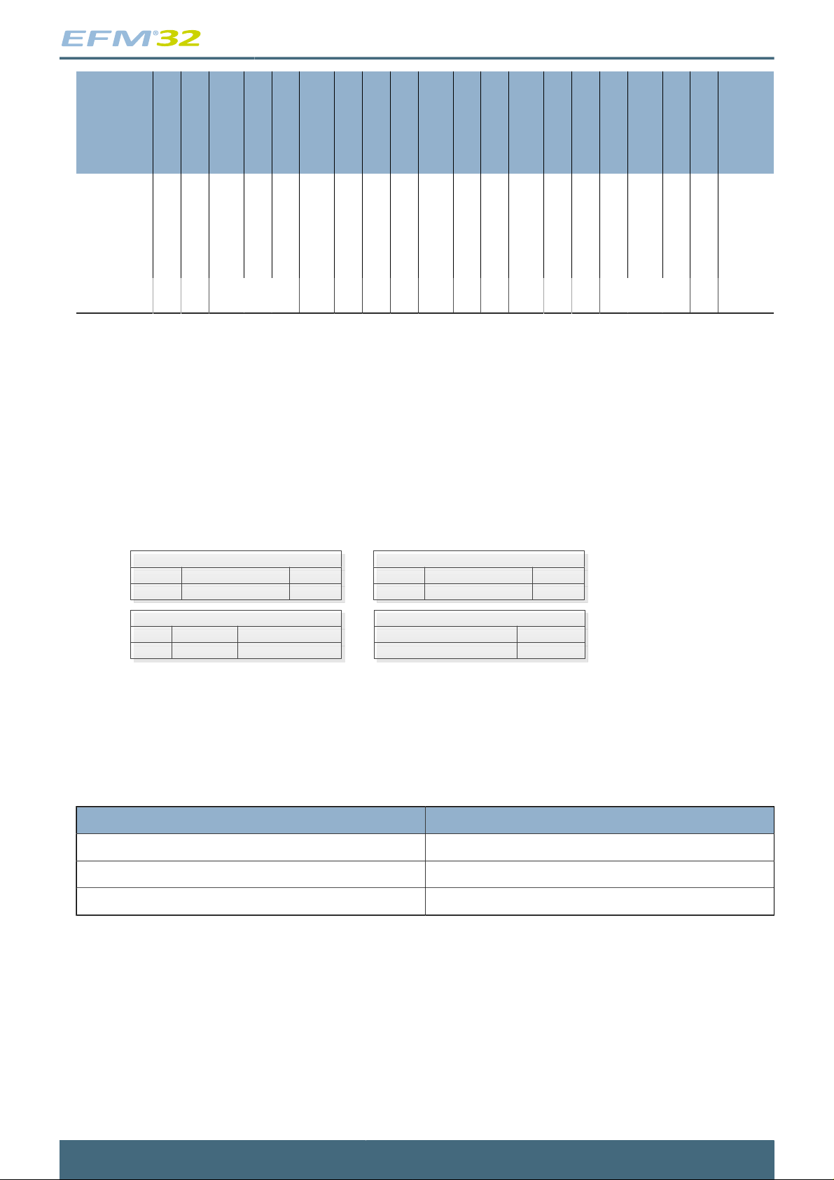
Tip
Throughout this document, the first figure in every module description contains an Energy Mode
Indicator showing which energy mode(s) the module can operate (see Table 3.1 (p. 8) ).
2014-07-02 - Tiny Gecko Family - d0034_Rev1.20 7
1 2 3 4
0
www.silabs.com
Page 8
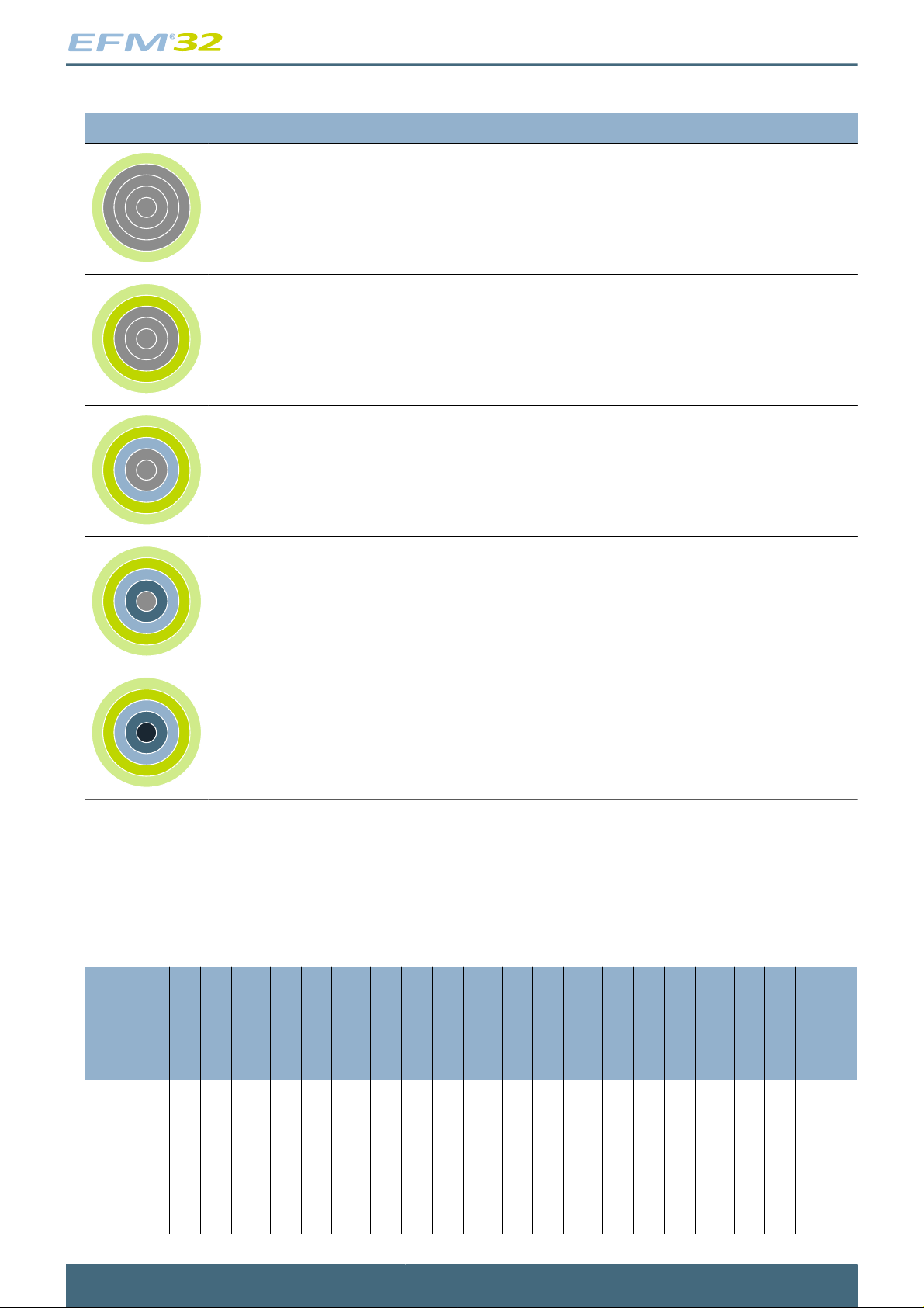
Table 3.1. Energy Mode Description
Energy Mode Name Description
...the world's most energy friendly microcontrollers
1 2 3 4
0
1 2 3 4
0
1 2 3 4
0
1 2 3 4
0
EM0 – Energy Mode 0
(Run mode)
EM1 – Energy Mode 1
(Sleep Mode)
EM2 – Energy Mode 2
(Deep Sleep Mode)
EM3 - Energy Mode 3
(Stop Mode)
In EM0, the CPU is running and consuming as little as 150 µA/MHz, when
running code from flash. All peripherals can be active.
In EM1, the CPU is sleeping and the power consumption is only 51 µA/MHz.
All peripherals, including DMA, PRS and memory system, are still available.
In EM2 the high frequency oscillator is turned off, but with the 32.768 kHz
oscillator running, selected low energy peripherals (LCD, RTC, LETIMER,
PCNT, LEUART, I2C, LESENSE, OPAMP, WDOG and ACMP) are still
available. This gives a high degree of autonomous operation with a current
consumption as low as 1.0 µA with RTC enabled. Power-on Reset, Brown-out
Detection and full RAM and CPU retention is also included.
In EM3, the low-frequency oscillator is disabled, but there is still full CPU
and RAM retention, as well as Power-on Reset, Pin reset, EM4 wake-up
and Brown-out Detection, with a consumption of only 0.6 µA. The low-power
ACMP, asynchronous external interrupt, PCNT, and I2C can wake-up the
device. Even in this mode, the wake-up time is a few microseconds.
1 2 3 4
0
EM4 – Energy Mode 4
(Shutoff Mode)
In EM4, the current is down to 20 nA and all chip functionality is turned off
except the pin reset, GPIO pin wake-up, GPIO pin retention and the PowerOn Reset. All pins are put into their reset state.
3.5 Product Overview
Table 3.2 (p. 8) shows a device overview of the EFM32TG Microcontroller Series, including
peripheral functionality. For more information, the reader is referred to the device specific datasheets.
Table 3.2. EFM32TG Microcontroller Series
C
EFM32TG Part
#
108F4 4 1 17 - 1 1 1
108F8 8 2 17 - 1 1 1
108F16 16 4 17 - 1 1 1
108F32 32 4 17 - 1 1 1
Flash
RAM
GPIO(pins)
LCD
USART
2
LEUART
I
Timer(PWM)
LETIMER
RTC
PCNT
2
1 1 1 1 - -
(6)
2
1 1 1 1 - -
(6)
2
1 1 1 1 - -
(6)
2
1 1 1 1 - -
(6)
Watchdog
ADC(pins)
DAC(pins)
ACMP(pins)
2
(4)
2
(4)
2
(4)
2
(4)
AES
EBI
LESENSE
Op-Amps
- - Y - QFN24
- - Y - QFN24
- - Y - QFN24
- - Y - QFN24
Package
2014-07-02 - Tiny Gecko Family - d0034_Rev1.20 8
www.silabs.com
Page 9

EFM32TG Part
#
110F4 4 1 17 - 1 1 1
110F8 8 2 17 - 1 1 1
110F16 16 4 17 - 1 1 1
110F32 32 4 17 - 1 1 1
210F8 8 2 24 - 2 1 1
210F16 16 4 24 - 2 1 1
210F32 32 4 24 - 2 1 1
222F8 8 2 37 - 2 1 1
222F16 16 4 37 - 2 1 1
222F32 32 4 37 - 2 1 1
225F8 8 2 37 - 2 1 1
225F16 16 4 37 - 2 1 1
225F32 32 4 37 - 2 1 1
230F8 8 2 56 - 2 1 1
230F16 16 4 56 - 2 1 1
230F32 32 4 56 - 2 1 1
232F8 8 2 53 - 2 1 1
232F16 16 4 53 - 2 1 1
232F32 32 4 53 - 2 1 1
822F8 8 2 37 Y 2 1 1
822F16 16 4 37 Y 2 1 1
822F32 32 4 37 Y 2 1 1
825F8 8 2 37 Y 2 1 1
825F16 16 4 37 Y 2 1 1
825F32 32 4 37 Y 2 1 1
840F8 8 2 56 Y 2 1 1
840F16 16 4 56 Y 2 1 1
Flash
RAM
GPIO(pins)
LCD
USART
LEUART
C
2
I
(6)
(6)
(6)
(6)
(6)
(6)
(6)
(6)
(6)
(6)
(6)
(6)
(6)
(6)
(6)
(6)
(6)
(6)
(6)
(6)
(6)
(6)
(6)
(6)
(6)
(6)
(6)
...the world's most energy friendly microcontrollers
Timer(PWM)
LETIMER
RTC
PCNT
Watchdog
ADC(pins)
DAC(pins)
ACMP(pins)
AES
EBI
LESENSE
Op-Amps
2
1 1 1 1 1 (2)
2
1 1 1 1 1 (2)
2
1 1 1 1 1 (2)
2
1 1 1 1 1 (2)
2
1 1 1 1 1 (4)
2
1 1 1 1 1 (4)
2
1 1 1 1 1 (4)
2
1 1 1 1 1 (4)
2
1 1 1 1 1 (4)
2
1 1 1 1 1 (4)
2
1 1 1 1 1 (4)
2
1 1 1 1 1 (4)
2
1 1 1 1 1 (4)
2
1 1 1 1 1 (8)
2
1 1 1 1 1 (8)
2
1 1 1 1 1 (8)
2
1 1 1 1 1 (8)
2
1 1 1 1 1 (8)
2
1 1 1 1 1 (8)
2
1 1 1 1 1 (5)
2
1 1 1 1 1 (5)
2
1 1 1 1 1 (5)
2
1 1 1 1 1 (5)
2
1 1 1 1 1 (5)
2
1 1 1 1 1 (5)
2
1 1 1 1 1 (8)
2
1 1 1 1 1 (8)
2
(1)2(4)
2
(1)2(4)
2
(1)2(4)
2
(1)2(4)
2
(1)2(5)
2
(1)2(5)
2
(1)2(5)
2
(1)2(12)
2
(1)2(12)
2
(1)2(12)
2
(1)2(12)
2
(1)2(12)
2
(1)2(12)
2
(2)2(16)
2
(2)2(16)
2
(2)2(16)
2
(2)2(16)
2
(2)2(16)
2
(2)2(16)
2
(1)2(4)
2
(1)2(4)
2
(1)2(4)
2
(1)2(4)
2
(1)2(4)
2
(1)2(4)
2
(2)2(8)
2
(2)2(8)
Y - Y 3 QFN24
Y - Y 3 QFN24
Y - Y 3 QFN24
Y - Y 3 QFN24
Y - Y 3 QFN32
Y - Y 3 QFN32
Y - Y 3 QFN32
Y - Y 3 QFP48
Y - Y 3 QFP48
Y - Y 3 QFP48
Y - Y 3 BGA48
Y - Y 3 BGA48
Y - Y 3 BGA48
Y - Y 3 QFN64
Y - Y 3 QFN64
Y - Y 3 QFN64
Y - Y 3 QFP64
Y - Y 3 QFP64
Y - Y 3 QFP64
Y - Y 3 QFP48
Y - Y 3 QFP48
Y - Y 3 QFP48
Y - Y 3 BGA48
Y - Y 3 BGA48
Y - Y 3 BGA48
Y - Y 3 QFN64
Y - Y 3 QFN64
Package
2014-07-02 - Tiny Gecko Family - d0034_Rev1.20 9
www.silabs.com
Page 10
...the world's most energy friendly microcontrollers
C
EFM32TG Part
#
840F32 32 4 56 Y 2 1 1
842F8 8 2 53 Y 2 1 1
842F16 16 4 53 Y 2 1 1
842F32 32 4 53 Y 2 1 1
Flash
RAM
GPIO(pins)
LCD
USART
2
LEUART
I
Timer(PWM)
LETIMER
RTC
2
1 1 1 1 1 (8)
(6)
2
1 1 1 1 1 (8)
(6)
2
1 1 1 1 1 (8)
(6)
2
1 1 1 1 1 (8)
(6)
PCNT
Watchdog
ADC(pins)
DAC(pins)
ACMP(pins)
2
(2)2(8)
2
(2)2(8)
2
(2)2(8)
2
(2)2(8)
AES
EBI
LESENSE
Op-Amps
Y - Y 3 QFN64
Y - Y 3 QFP64
Y - Y 3 QFP64
Y - Y 3 QFP64
3.6 Device Revision
The device revision number is read from the ROM Table. The major revision number and the chip family
number is read from PID0 and PID1 registers. The minor revision number is extracted from the PID2 and
PID3 registers, as illustrated in Figure 3.3 (p. 10) . The Fam[5:2] and Fam[1:0] must be combined
to complete the chip family number, while the Minor Rev[7:4] and Minor Rev[3:0] must be combined to
form the complete revision number.
Package
Figure 3.3. Revision Number Extraction
PID2 (0xE00FFFE8)
31:8 7:4
3:0
Minor Rev[7:4]
PID0 (0xE00FFFE0)
31:7 6:5
Fam[1:0] Fam[5:2]
5:0
Major Rev[5:0]
PID3 (0xE00FFFEC)
31:8 7:4
Minor Rev[3:0]
PID1 (0xE00FFFE4)
31:4
3:0
3:0
For the latest revision of the Tiny Gecko family, the chip family number is 0x01 and the major revision
number is 0x01. The minor revision number is to be interpreted according to Table 3.3 (p. 10) .
Table 3.3. Minor Revision Number Interpretation
Minor Rev[7:0] Revision
0x00 A
0x01 B
0x02 C
2014-07-02 - Tiny Gecko Family - d0034_Rev1.20 10
www.silabs.com
Page 11

4 System Processor
1 2 3 4
0
...the world's most energy friendly microcontrollers
Quick Facts
What?
The industry leading Cortex-M3 processor
from ARM is the CPU in the EFM32TG
microcontrollers.
Why?
The ARM Cortex-M3 is designed for
exceptional short response time, high
code density, and high 32-bit throughput
while maintaining a strict cost and power
consumption budget.
How?
Combined with the ultra low energy
peripherals available, the Cortex-M3 makes
the EFM32TG devices perfect for 8- to 32bit applications. The processor is featuring a
Harvard architecture, 3 stage pipeline, single
cycle instructions, Thumb-2 instruction set
support, and fast interrupt handling.
4.1 Introduction
The ARM Cortex-M3 32-bit RISC processor provides outstanding computational performance and
exceptional system response to interrupts while meeting low cost requirements and low power
consumption.
The ARM Cortex-M3 implemented is revision r2p1.
4.2 Features
• Harvard Architecture
• Separate data and program memory buses (No memory bottleneck as for a single-bus system)
• 3-stage pipeline
• Thumb-2 instruction set
• Enhanced levels of performance, energy efficiency, and code density
• Single-cycle multiply and efficient divide instructions
• 32-bit multiplication in a single cycle
• Signed and unsigned divide operations between 2 and 12 cycles
• Atomic bit manipulation with bit banding
• Direct access to single bits of data
• Two 1MB bit banding regions for memory and peripherals mapping to 32MB alias regions
• Atomic operation which cannot be interrupted by other bus activities
• 1.25 DMIPS/MHz
• 24-bit System Tick Timer for Real-Time Operating System (RTOS)
• Excellent 32-bit migration choice for 8/16 bit architecture based designs
• Simplified stack-based programmer's model is compatible with traditional ARM architecture and
retains the programming simplicity of legacy 8- and 16-bit architectures
• Unaligned data storage and access
2014-07-02 - Tiny Gecko Family - d0034_Rev1.20 11
www.silabs.com
Page 12
...the world's most energy friendly microcontrollers
• Continuous storage of data requiring different byte lengths
• Data access in a single core clock cycle
• Integrated power modes
• Sleep Now mode for immediate transfer to low power state
• Sleep on Exit mode for entry into low power state after the servicing of an interrupt
• Ability to extend power savings to other system components
• Optimized for low latency, nested interrupts
4.3 Functional Description
For a full functional description of the ARM Cortex-M3 (r2p1) implementation in the EFM32TG family,
the reader is referred to the EFM32 Cortex-M3 Reference Manual.
4.3.1 Interrupt Operation
Figure 4.1. Interrupt Operation
Module Cortex- M3 NVIC
IFS[n] IFC[n]
Interrupt
condition
set clear
IF[n]
IEN[n]
IRQ
SETENA[n]/ CLRENA[n]
Active interrupt
set clear
SETPEND[n]/ CLRPEND[n]
Software generated interrupt
Interrupt
request
The EFM32TG devices have up to 23 interrupt request lines (IRQ) which are connected to the CortexM3. Each of these lines (shown in Table 4.1 (p. 12) ) are connected to one or more interrupt flags in
one or more modules. The interrupt flags are set by hardware on an interrupt condition. It is also possible
to set/clear the interrupt flags through the IFS/IFC registers. Each interrupt flag is then qualified with its
own interrupt enable bit (IEN register), before being OR'ed with the other interrupt flags to generate the
IRQ. A high IRQ line will set the corresponding pending bit (can also be set/cleared with the SETPEND/
CLRPEND bits in ISPR0/ICPR0) in the Cortex-M3 NVIC. The pending bit is then qualified with an enable
bit (set/cleared with SETENA/CLRENA bits in ISER0/ICER0) before generating an interrupt request to
the core. Figure 4.1 (p. 12) illustrates the interrupt system. For more information on how the interrupts
are handled inside the Cortex-M3, the reader is referred to the EFM32 Cortex-M3 Reference Manual.
Table 4.1. Interrupt Request Lines (IRQ)
IRQ # Source
0 DMA
1 GPIO_EVEN
2 TIMER0
3 USART0_RX
4 USART0_TX
5 ACMP0/ACMP1
6 ADC0
7 DAC0
8 I2C0
9 GPIO_ODD
2014-07-02 - Tiny Gecko Family - d0034_Rev1.20 12
www.silabs.com
Page 13

...the world's most energy friendly microcontrollers
IRQ # Source
10 TIMER1
11 USART1_RX
12 USART1_TX
13 LESENSE
14 LEUART0
15 LETIMER0
16 PCNT0
17 RTC
18 CMU
19 VCMP
20 LCD
21 MSC
22 AES
2014-07-02 - Tiny Gecko Family - d0034_Rev1.20 13
www.silabs.com
Page 14
...the world's most energy friendly microcontrollers
5 Memory and Bus System
1 2 3 4
0
Flash
ARM Cortex- M3
RAM
Peripherals
DMA Controller
Quick Facts
What?
A low latency memory system, including low
energy flash and RAM with data retention,
makes extended use of low-power energymodes possible.
Why?
RAM retention reduces the need for storing
data in flash and enables frequent use of the
ultra low energy modes EM2 and EM3 with
as little as 0.6 µA current consumption.
How?
Low energy and non-volatile flash memory
stores program and application data
in all energy modes and can easily be
reprogrammed in system. Low leakage RAM,
with data retention in EM0 to EM3, removes
the data restore time penalty, and the DMA
ensures fast autonomous transfers with
predictable response time.
5.1 Introduction
The EFM32TG contains an AMBA AHB Bus system allowing bus masters to access the memory mapped
address space. A multilayer AHB bus matrix, using a Round-robin arbitration scheme, connects the
master bus interfaces to the AHB slaves (Figure 5.1 (p. 15) ). The bus matrix allows several AHB
slaves to be accessed simultaneously. An AMBA APB interface is used for the peripherals, which are
accessed through an AHB-to-APB bridge connected to the AHB bus matrix. The AHB bus masters are:
• Cortex-M3 ICode: Used for instruction fetches from Code memory (0x00000000 - 0x1FFFFFFF).
• Cortex-M3 DCode: Used for debug and data access to Code memory (0x00000000 - 0x1FFFFFFF).
• Cortex-M3 System: Used for instruction fetches, data and debug access to system space
(0x20000000 - 0xDFFFFFFF).
• DMA: Can access SRAM, Flash and peripherals (0x00000000 - 0xDFFFFFFF).
2014-07-02 - Tiny Gecko Family - d0034_Rev1.20 14
www.silabs.com
Page 15
Figure 5.1. EFM32TG Bus System
...the world's most energy friendly microcontrollers
Cortex
ICode
DCode
System
DMA
AHB Multilayer
Bus Matrix
5.2 Functional Description
Flash
RAM
AES
AHB/APB
Bridge
Peripheral 0
Peripheral n
The memory segments are mapped together with the internal segments of the Cortex-M3 into the system
memory map shown by Figure 5.2 (p. 16)
2014-07-02 - Tiny Gecko Family - d0034_Rev1.20 15
www.silabs.com
Page 16
Figure 5.2. System Address Space
...the world's most energy friendly microcontrollers
The embedded SRAM is located at address 0x20000000 in the memory map of the EFM32TG. When
running code located in SRAM starting at this address, the Cortex-M3 uses the System bus to fetch
instructions. This results in reduced performance as the Cortex-M3 accesses stack, other data in SRAM
and peripherals using the System bus. To be able to run code from SRAM efficiently, the SRAM is also
mapped in the code space at address 0x10000000. When running code from this space, the Cortex-M3
fetches instructions through the I/D-Code bus interface, leaving the System bus for data access. The
SRAM mapped into the code space can however only be accessed by the CPU, i.e. not the DMA.
5.2.1 Bit-banding
The SRAM bit-band alias and peripheral bit-band alias regions are located at 0x22000000 and
0x42000000 respectively. Read and write operations to these regions are converted into masked singlebit reads and atomic single-bit writes to the embedded SRAM and peripherals of the EFM32TG.
The standard approach to modify a single register or SRAM bit in the aliased regions, requires software
to read the value of the byte, half-word or word containing the bit, modify the bit, and then write the byte,
half-word or word back to the register or SRAM address. Using bit-banding, this read-modify-write can
be done in a single atomic operation. As read-writeback, bit-masking and bit-shift operations are not
necessary in software, code size is reduced and execution speed improved.
The bit-band regions allows addressing each individual bit in the SRAM and peripheral areas of the
memory map. To set or clear a bit in the embedded SRAM, write a 1 or a 0 to the following address:
Memory SRAM Area Set/Clear Bit
2014-07-02 - Tiny Gecko Family - d0034_Rev1.20 16
www.silabs.com
Page 17

...the world's most energy friendly microcontrollers
bit_address = 0x22000000 + (address – 0x20000000) × 32 + bit × 4, (5.1)
where address is the address of the 32-bit word containing the bit to modify, and bit is the index of the
bit in the 32-bit word.
To modify a bit in the Peripheral area, use the following address:
Memory Peripheral Area Bit Modification
bit_address = 0x42000000 + (address – 0x40000000) × 32 + bit × 4, (5.2)
where address and bit are defined as above.
Note that the AHB-peripheral AES does not support bit-banding.
5.2.2 Peripherals
The peripherals are mapped into the peripheral memory segment, each with a fixed size address range
according to Table 5.1 (p. 17) , Table 5.2 (p. 18) and Table 5.3 (p. 19) .
Table 5.1. Memory System Core Peripherals
Core peripherals
Address range Peripheral
0x400E0400 – 0x41FFFFFF Reserved
0x400E0000 – 0x400E03FF AES
0x400CC400 – 0x400FFFFF Reserved
0x400CC000 – 0x400CC3FF PRS
0x400CA400 – 0x400CBFFF Reserved
0x400CA000 – 0x400CA3FF RMU
0x400C8400 – 0x400C9FFF Reserved
0x400C8000 – 0x400C83FF CMU
0x400C6400 – 0x400C7FFF Reserved
0x400C6000 – 0x400C63FF EMU
0x400C4000 – 0x400C5FFF Reserved
0x400C2000 – 0x400C3FFF DMA
0x400C0400 – 0x400C1FFF Reserved
0x400C0000 – 0x400C03FF MSC
2014-07-02 - Tiny Gecko Family - d0034_Rev1.20 17
www.silabs.com
Page 18

...the world's most energy friendly microcontrollers
Table 5.2. Memory System Low Energy Peripherals
Low energy peripherals
Address range Peripheral
0x4008A400 – 0x400BFFFF Reserved
0x4008C000 – 0x4008C3FF LESENSE
0x4008A000 – 0x4008A3FF LCD
0x40088400 – 0x40089FFF Reserved
0x40088000 – 0x400883FF WDOG
0x40086C00 – 0x40087FFF Reserved
0x40086000 – 0x400863FF PCNT0
0x40084800 – 0x40085FFF Reserved
0x40084000 – 0x400843FF LEUART0
0x40082400 – 0x40083FFF Reserved
0x40082000 – 0x400823FF LETIMER0
0x40080400 – 0x40081FFF Reserved
0x40080000 – 0x400803FF RTC
2014-07-02 - Tiny Gecko Family - d0034_Rev1.20 18
www.silabs.com
Page 19

...the world's most energy friendly microcontrollers
Table 5.3. Memory System Peripherals
Peripherals
Address range Peripheral
0x40010C00 – 0x4007FFFF Reserved
0x40010400 – 0x400107FF TIMER1
0x40010000 – 0x400103FF TIMER0
0x4000E400 – 0x4000FFFF Reserved
0x4000CC00 – 0x4000DFFF Reserved
0x4000C400 – 0x4000C7FF USART1
0x4000C000 – 0x4000C3FF USART0
0x4000A400 – 0x4000BFFF Reserved
0x4000A000 – 0x4000A3FF I2C0
0x40008400 – 0x40009FFF Reserved
0x40007000 – 0x40007FFF Reserved
0x40006000 – 0x40006FFF GPIO
0x40004400 – 0x40005FFF Reserved
0x40004000 – 0x400043FF DAC0
0x40002400 – 0x40003FFF Reserved
0x40002000 – 0x400023FF ADC0
0x40001800 – 0x40001FFF Reserved
0x40001400 – 0x400017FF ACMP1
0x40001000 – 0x400013FF ACMP0
0x40000400 – 0x40000FFF Reserved
0x40000000 - 0x400003FF VCMP
5.2.3 Bus Matrix
The Bus Matrix connects the memory segments to the bus masters:
• Code: CPU instruction or data fetches from the code space
• System: CPU read and write to the SRAM and peripherals
• DMA: Access to SRAM, Flash and peripherals
5.2.3.1 Arbitration
The Bus Matrix uses a round-robin arbitration algorithm which enables high throughput and low latency
while starvation of simultaneous accesses to the same bus slave are eliminated. Round-robin does not
assign a fixed priority to each bus master. The arbiter does not insert any bus wait-states.
5.2.3.2 Access Performance
The Bus Matrix is a multi-layer energy optimized AMBA AHB compliant bus with an internal bandwidth
equal to 4 times a single AHB-bus.
2014-07-02 - Tiny Gecko Family - d0034_Rev1.20 19
www.silabs.com
Page 20

...the world's most energy friendly microcontrollers
The Bus Matrix accepts new transfers initiated by each master in every clock cycle without inserting
any wait-states. The slaves, however, may insert wait-states depending on their internal throughput and
the clock frequency.
The Cortex-M3, the DMA Controller, and the peripherals run on clocks that can be prescaled separately.
When accessing a peripheral which runs on a frequency equal to or faster than the HFCORECLK, the
number of wait cycles per access, in addition to master arbitration, is given by:
Memory Wait Cycles with Clock Equal or Faster than HFCORECLK
where N
slave cycles
N
is the wait cycles introduced by the slave.
cycles
= 2 + N
slave cycles
, (5.3)
When accessing a peripheral running on a clock slower than the HFCORECLK, wait-cycles are
introduced to allow the transfer to complete on the peripheral clock. The number of wait cycles per
access, in addition to master arbitration, is given by:
Memory Wait Cycles with Clock Slower than CPU
N
where N
slave cycles
is the number of wait cycles introduced by the slave.
For general register access, N
cycles
= (2 + N
slave cycles
slave cycles
= 1.
) x f
HFCORECLK/fHFPERCLK
, (5.4)
More details on clocks and prescaling can be found in Chapter 11 (p. 99) .
5.3 Access to Low Energy Peripherals (Asynchronous Registers)
5.3.1 Introduction
The Low Energy Peripherals are capable of running when the high frequency oscillator and core system
is powered off, i.e. in energy mode EM2 and in some cases also EM3. This enables the peripherals to
perform tasks while the system energy consumption is minimal.
The Low Energy Peripherals are:
• Liquid Crystal Display driver - LCD
• Low Energy Timer - LETIMER
• Low Energy UART - LEUART
• Pulse Counter - PCNT
• Real Time Counter - RTC
• Watchdog - WDOG
• Low Energy Sensor Interface - LESENSE
All Low Energy Peripherals are memory mapped, with automatic data synchronization. Because the Low
Energy Peripherals are running on clocks asynchronous to the core clock, there are some constraints
on how register accesses can be done, as described in the following sections.
5.3.1.1 Writing
Every Low Energy Peripheral has one or more registers with data that needs to be synchronized into
the Low Energy clock domain to maintain data consistency and predictable operation. There are two
2014-07-02 - Tiny Gecko Family - d0034_Rev1.20 20
www.silabs.com
Page 21

...the world's most energy friendly microcontrollers
different synchronization mechanisms on the Tiny Gecko; immediate synchronization, and delayed
synchronization. Immediate synchronization is available for the RTC, LETIMER and LESENSE, and
results in an immediate update of the target registers. Delayed synchronization is used for the other
Low Energy Peripherals, and for these peripherals, a write operation requires 3 positive edges on the
clock of the Low Energy Peripheral being accessed. Registers requiring synchronization are marked
"Asynchronous" in their description header.
5.3.1.1.1 Delayed synchronization
After writing data to a register which value is to be synchronized into the Low Energy Peripheral using
delayed synchronization, a corresponding busy flag in the <module_name>_SYNCBUSY register (e.g.
LEUART_SYNCBUSY) is set. This flag is set as long as synchronization is in progress and is cleared
upon completion.
Note
Subsequent writes to the same register before the corresponding busy flag is cleared is not
supported. Write before the busy flag is cleared may result in undefined behavior.
In general, the SYNCBUSY register only needs to be observed if there is a risk of multiple
write access to a register (which must be prevented). It is not required to wait until the
relevant flag in the SYNCBUSY register is cleared after writing a register. E.g EM2 can be
entered immediately after writing a register.
See Figure 5.3 (p. 21) for a more detailed overview of the write operation.
Figure 5.3. Write operation to Low Energy Peripherals
Core Clock Domain Low Frequency Clock Domain
Write[0:n]
Set 0
Set 1
Set n
Core Clock
Register 0
Register 1
.
.
.
Register n
Syncbusy Register 0
Syncbusy Register 1
.
.
.
Syncbusy Register n
Freeze
Clear 0
Clear 1
Clear n
Low Frequency Clock Low Frequency Clock
Synchronizer 0
Synchronizer 1
.
.
.
Synchronizer n
Synchronization Done
Register 0 Sync
Register 1 Sync
.
.
.
Register n Sync
5.3.1.1.2 Immediate synchronization
Contrary to the peripherals with delayed synchronization, data written to peripherals with immediate
synchronization, takes effect in the peripheral immediately. They are updated immediately on the
peripheral write access. If a write is set up close to a peripheral clock edge, the write is delayed to after
the clock edge. This will introduce wait-states on peripheral access. In the worst case, there can be three
wait-state cycles of the HFCORECLK_LE and an additional wait-state equivalent of up to 315 ns.
For peripherals with immediate synchronization, the SYNCBUSY registers are still present and serve two
purposes: (1) commands written to a peripheral with immediate synchronization are not executed before
the first peripheral clock after the write. During this period, the SYNCBUSY flag in the command register
2014-07-02 - Tiny Gecko Family - d0034_Rev1.20 21
www.silabs.com
Page 22
...the world's most energy friendly microcontrollers
is set, indicating that the command has not yet been executed; (2) to maintain backwards compatibility
with the EFM32G series, SYNCBUSY registers are also present for other registers. These are however,
always 0, indicating that register writes are always safe.
Note
If the application must be compatible with the EFM32G series, all Low Energy Peripherals
should be accessed as if they only had delayed synchronization, i.e. using SYNCBUSY.
5.3.1.2 Reading
When reading from Low Energy Peripherals, the data is synchronized regardless of the originating clock
domain. Registers updated/maintained by the Low Energy Peripheral are read directly from the Low
Energy clock domain. Registers residing in the core clock domain, are read from the core clock domain.
See Figure 5.4 (p. 22) for a more detailed overview of the read operation.
Note
Writing a register and then immediately reading back the value of the register may give the
impression that the write operation is complete. This is not necessarily the case. Please
refer to the SYNCBUSY register for correct status of the write operation to the Low Energy
Peripheral.
Figure 5.4. Read operation from Low Energy Peripherals
Core Clock Domain Low Frequency Clock Domain
Core Clock
Register 0
Register 1
Register n
Read
Synchronizer
Read Data
Freeze
.
.
.
Low Frequency Clock Low Frequency Clock
Synchronizer 0
Synchronizer 1
.
.
.
Synchronizer n
HW Status Register 0
HW Status Register 1
.
.
.
HW Status Register m
Register 0 Sync
Register 1 Sync
.
.
.
Register n Sync
Low Energy
Peripheral
Main
Function
5.3.2 FREEZE register
For Low Energy Peripherals with delayed synchronization there is a <module_name>_FREEZE register
(e.g. RTC_FREEZE), containing a bit named REGFREEZE. If precise control of the synchronization
process is required, this bit may be utilized. When REGFREEZE is set, the synchronization process is
halted, allowing the software to write multiple Low Energy registers before starting the synchronization
process, thus providing precise control of the module update process. The synchronization process is
started by clearing the REGFREEZE bit.
Note
The FREEZE register is also present on peripherals with immediate synchronization, but
has no effect.
2014-07-02 - Tiny Gecko Family - d0034_Rev1.20 22
www.silabs.com
Page 23

...the world's most energy friendly microcontrollers
5.4 Flash
The Flash retains data in any state and typically stores the application code, special user data and
security information. The Flash memory is typically programmed through the debug interface, but can
also be erased and written to from software.
• Up to 32 kB of memory
• Page size of 512 bytes (minimum erase unit)
• Minimum 20 000 erase cycles
• More than 10 years data retention at 85°C
• Lock-bits for memory protection
• Data retention in any state
5.5 SRAM
The primary task of the SRAM memory is to store application data. Additionally, it is possible to execute
instructions from SRAM, and the DMA may used to transfer data between the SRAM, Flash and
peripherals.
• Up to 4 kB memory
• Bit-band access support
• 4 kB blocks may be individually powered down when not in use
• Data retention of the entire memory in EM0 to EM3
5.6 Device Information (DI) Page
The DI page contains calibration values, a unique identification number and other useful data. See the
table below for a complete overview.
Table 5.4. Device Information Page Contents
DI Address Register Description
0x0FE08020 CMU_LFRCOCTRL Register reset value.
0x0FE08028 CMU_HFRCOCTRL Register reset value.
0x0FE08030 CMU_AUXHFRCOCTRL Register reset value.
0x0FE08040 ADC0_CAL Register reset value.
0x0FE08048 ADC0_BIASPROG Register reset value.
0x0FE08050 DAC0_CAL Register reset value.
0x0FE08058 DAC0_BIASPROG Register reset value.
0x0FE08060 ACMP0_CTRL Register reset value.
0x0FE08068 ACMP1_CTRL Register reset value.
0x0FE08078 CMU_LCDCTRL Register reset value.
0x0FE080A0 DAC0_OPACTRL Register reset value
0x0FE080A8 DAC0_OPAOFFSET Register reset value
0x0FE081B0 DI_CRC [15:0]: DI data CRC-16.
0x0FE081B2 CAL_TEMP_0 [7:0] Calibration temperature (°C).
0x0FE081B4 ADC0_CAL_1V25 [14:8]: Gain for 1V25 reference, [6:0]: Offset for 1V25
reference.
2014-07-02 - Tiny Gecko Family - d0034_Rev1.20 23
www.silabs.com
Page 24

...the world's most energy friendly microcontrollers
DI Address Register Description
0x0FE081B6 ADC0_CAL_2V5 [14:8]: Gain for 2V5 reference, [6:0]: Offset for 2V5
reference.
0x0FE081B8 ADC0_CAL_VDD [14:8]: Gain for VDD reference, [6:0]: Offset for VDD
reference.
0x0FE081BA ADC0_CAL_5VDIFF [14:8]: Gain for 5VDIFF reference, [6:0]: Offset for 5VDIFF
reference.
0x0FE081BC ADC0_CAL_2XVDD [14:8]: Reserved (gain for this reference cannot be
calibrated), [6:0]: Offset for 2XVDD reference.
0x0FE081BE ADC0_TEMP_0_READ_1V25 [15:4] Temperature reading at 1V25 reference, [3:0]
Reserved.
0x0FE081C8 DAC0_CAL_1V25 [22:16]: Gain for 1V25 reference, [13:8]: Channel 1 offset for
1V25 reference, [5:0]: Channel 0 offset for 1V25 reference.
0x0FE081CC DAC0_CAL_2V5 [22:16]: Gain for 2V5 reference, [13:8]: Channel 1 offset for
2V5 reference, [5:0]: Channel 0 offset for 2V5 reference.
0x0FE081D0 DAC0_CAL_VDD [22:16]: Reserved (gain for this reference cannot be
calibrated), [13:8]: Channel 1 offset for VDD reference, [5:0]:
Channel 0 offset for VDD reference.
0x0FE081D4 AUXHFRCO_CALIB_BAND_1 [7:0]: Tuning for the 1.2 MHZ AUXHFRCO band.
0x0FE081D5 AUXHFRCO_CALIB_BAND_7 [7:0]: Tuning for the 6.6 MHZ AUXHFRCO band.
0x0FE081D6 AUXHFRCO_CALIB_BAND_11 [7:0]: Tuning for the 11 MHZ AUXHFRCO band.
0x0FE081D7 AUXHFRCO_CALIB_BAND_14 [7:0]: Tuning for the 14 MHZ AUXHFRCO band.
0x0FE081D8 AUXHFRCO_CALIB_BAND_21 [7:0]: Tuning for the 21 MHZ AUXHFRCO band.
0x0FE081D9 AUXHFRCO_CALIB_BAND_28 [7:0]: Tuning for the 28 MHZ AUXHFRCO band.
0x0FE081DC HFRCO_CALIB_BAND_1 [7:0]: Tuning for the 1.2 MHZ HFRCO band.
0x0FE081DD HFRCO_CALIB_BAND_7 [7:0]: Tuning for the 6.6 MHZ HFRCO band.
0x0FE081DE HFRCO_CALIB_BAND_11 [7:0]: Tuning for the 11 MHZ HFRCO band.
0x0FE081DF HFRCO_CALIB_BAND_14 [7:0]: Tuning for the 14 MHZ HFRCO band.
0x0FE081E0 HFRCO_CALIB_BAND_21 [7:0]: Tuning for the 21 MHZ HFRCO band.
0x0FE081E1 HFRCO_CALIB_BAND_28 [7:0]: Tuning for the 28 MHZ HFRCO band.
0x0FE081E7 MEM_INFO_PAGE_SIZE [7:0] Flash page size in bytes coded as 2 ^
((MEM_INFO_PAGE_SIZE + 10) & 0xFF). Ie. the value
0xFF = 512 bytes.
0x0FE081F0 UNIQUE_0 [31:0] Unique number.
0x0FE081F4 UNIQUE_1 [63:32] Unique number.
0x0FE081F8 MEM_INFO_FLASH [15:0]: Flash size, kbyte count as unsigned integer (eg.
128).
0x0FE081FA MEM_INFO_RAM [15:0]: Ram size, kbyte count as unsigned integer (eg. 16).
0x0FE081FC PART_NUMBER [15:0]: EFM32 part number as unsigned integer (eg. 230).
0x0FE081FE PART_FAMILY [7:0]: EFM32 part family number (Gecko = 71, Giant Gecko
= 72, Tiny Gecko = 73, Leopard Gecko=74, Wonder
Gecko=75).
0x0FE081FF PROD_REV [7:0]: EFM32 Production ID.
2014-07-02 - Tiny Gecko Family - d0034_Rev1.20 24
www.silabs.com
Page 25
6 DBG - Debug Interface
1 2 3 4
0
ARM Cortex- M3
DBG
Debug Data
...the world's most energy friendly microcontrollers
Quick Facts
What?
The DBG (Debug Interface) is used to
program and debug EFM32TG devices.
Why?
The Debug Interface makes it easy to reprogram and update the system in the field,
and allows debugging with minimal I/O pin
usage.
How?
The Cortex-M3 supports advanced
debugging features. EFM32TG devices
only use two port pins for debugging or
programming. The internal and external state
of the system can be examined with debug
extensions supporting instruction or data
access break- and watch points.
6.1 Introduction
The EFM32TG devices include hardware debug support through a 2-pin serial-wire debug (SWD)
interface. In addition, there is also a Serial Wire Viewer pin which can be used to output profiling
information, data trace and software-generated messages.
For more technical information about the debug interface the reader is referred to:
• ARM Cortex-M3 Technical Reference Manual
• ARM CoreSight Components Technical Reference Manual
• ARM Debug Interface v5 Architecture Specification
6.2 Features
• Flash Patch and Breakpoint (FPB) unit
• Implement breakpoints and code patches
• Data Watch point and Trace (DWT) unit
• Implement watch points, trigger resources and system profiling
• Instrumentation Trace Macrocell (ITM)
• Application-driven trace source that supports printf style debugging
6.3 Functional Description
There are three debug pins and four trace pins available on the device. Operation of these pins are
described in the following section.
6.3.1 Debug Pins
The following pins are the debug connections for the device:
2014-07-02 - Tiny Gecko Family - d0034_Rev1.20 25
www.silabs.com
Page 26
...the world's most energy friendly microcontrollers
• Serial Wire Clock input (SWCLK): This pin is enabled after reset and has a built-in pull down.
• Serial Wire Data Input/Output (SWDIO): This pin is enabled after reset and has a built-in pull-up.
• Serial Wire Viewer (SWV): This pin is disabled after reset.
The debug pins can be enabled and disabled through GPIO_ROUTE, see Section 28.3.4.1 (p. 471)
. Please remeberer that upon disabling, debug contact with the device is lost. Also note that, because
the debug pins have pull-down and pull-up enabled by default, leaving them enabled might increase the
current consumption with up to 200 µA if left connected to supply or ground.
6.3.2 Debug and EM2/EM3
Leaving the debugger connected when issuing a WFI or WFE to enter EM2 or EM3 will make the system
enter a special EM2. This mode differs from regular EM2 and EM3 in that the high frequency clocks
are still enabled, and certain core functionality is still powered in order to maintain debug-functionality.
Because of this, the current consumption in this mode is closer to EM1 and it is therefore important to
disconnect the debugger before doing current consumption measurements.
6.4 Debug Lock and Device Erase
The debug access to the Cortex-M3 is locked by clearing the Debug Lock Word (DLW) and resetting
the device, see Section 7.3.2 (p. 32) .
When debug access is locked, the debug interface remains accessible but the connection to the CortexM3 core and the whole bus-system is blocked as shown in Figure 6.2 (p. 27) . This mechanism is
controlled by the Authentication Access Port (AAP) as illustrated by Figure 6.1 (p. 26) . The AAP is
only accessible from a debugger and not from the core.
Figure 6.1. AAP - Authentication Access Port
DEVICEERASE
ERASEBUSY
Cortex
SerialWire
debug
interface
DLW[3:0] = = 0xF
SW-DP AHB-AP
Authentication
Access Port
(AAP)
The debugger can access the AAP-registers, and only these registers just after reset, for the time of the
AAP-window outlined in Figure 6.2 (p. 27) . If the device is locked, access to the core and bus-system
is blocked even after code execution starts, and the debugger can only access the AAP-registers. If the
device is not locked, the AAP is no longer accessible after code execution starts, and the debugger can
access the core and bus-system normally. The AAP window can be extended by issuing the bit pattern
on SWDIO/SWCLK as shown in Figure 6.3 (p. 27) . This pattern should be applied just before reset
is deasserted, and will give the debugger more time to access the AAP.
2014-07-02 - Tiny Gecko Family - d0034_Rev1.20 26
www.silabs.com
Page 27
Figure 6.2. Device Unlock
Reset
Locked
No access
150 us
...the world's most energy friendly microcontrollers
Program
execution
AAP
Program
execution
Unlocked
Extended
unlocked
No access
No access
AAP
47 us
Extended AAP
255 x 47 us
Cortex
Program
execution
Cortex
Figure 6.3. AAP Expansion
SWDIO
SWCLK
AAP expand
If the device is locked, it can be unlocked by writing a valid key to the AAP_CMDKEY register and then
setting the DEVICEERASE bit of the AAP_CMD register via the debug interface. The commands are not
executed before AAP_CMDKEY is invalidated, so this register should be cleared to to start the erase
operation. This operation erases the main block of flash, all lock bits are reset and debug access through
the AHB-AP is enabled. The operation takes 40 ms to complete. Note that the SRAM contents will also
be deleted during a device erase, while the UD-page is not erased.
Even if the device is not locked, the can device can be erased through the AAP, using the above
procedure during the AAP window. This can be useful if the device has been programmed with code that,
e.g., disables the debug interface pins on start-up, or does something else that prevents communication
with a debugger.
If the device is locked, the debugger may read the status from the AAP_STATUS register. When the
ERASEBUSY bit is set low after DEVICEERASE of the AAP_CMD register is set, the debugger may
set the SYSRESETREQ bit in the AAP_CMD register. After reset, the debugger may resume a normal
debug session through the AHB-AP. If the device is not locked, the device erase starts when the AAP
window closes, so it is not possible to poll the status.
2014-07-02 - Tiny Gecko Family - d0034_Rev1.20 27
www.silabs.com
Page 28
...the world's most energy friendly microcontrollers
6.5 Register Map
The offset register address is relative to the registers base address.
Offset Name Type Description
0x000 AAP_CMD W1 Command Register
0x004 AAP_CMDKEY W1 Command Key Register
0x008 AAP_STATUS R Status Register
0x0FC AAP_IDR R AAP Identification Register
6.6 Register Description
6.6.1 AAP_CMD - Command Register
Offset Bit Position
0x000
Reset
Access
Name
31
30
29
28
272625
24
23
22
21
201918
17
16
15
141312
11
9
8
7
6
10
5
Bit Name Reset Access Description
31:2 Reserved
1 SYSRESETREQ 0 W1 System Reset Request
A system reset request is generated when set to 1. This register is write enabled from the AAP_CMDKEY register.
0 DEVICEERASE 0 W1 Erase the Flash Main Block, SRAM and Lock Bits
When set, all data and program code in the main block is erased, the SRAM is cleared and then the Lock Bit (LB) page is erased.
This also includes the Debug Lock Word (DLW), causing debug access to be enabled after the next reset. The information block
User Data page (UD) is left unchanged, but the User data page Lock Word (ULW) is erased. This register is write enabled from
the AAP_CMDKEY register.
To ensure compatibility with future devices, always write bits to 0. More information in Section 2.1 (p. 3)
6.6.2 AAP_CMDKEY - Command Key Register
4
3
2
1
0
0
0
W1
W1
SYSRESETREQ
DEVICEERASE
Offset Bit Position
0x004
Reset
Access
Name
31
30
29
28
272625
24
23
22
21
201918
17
16
15
0x00000000
W1
WRITEKEY
141312
Bit Name Reset Access Description
31:0 WRITEKEY 0x00000000 W1 CMD Key Register
2014-07-02 - Tiny Gecko Family - d0034_Rev1.20 28
9
8
7
6
5
4
3
2
1
11
10
0
www.silabs.com
Page 29
...the world's most energy friendly microcontrollers
Bit Name Reset Access Description
The key value must be written to this register to write enable the AAP_CMD register. After AAP_CMD is written, this register should
be cleared to excecute the command.
Value Mode Description
0xCFACC118 WRITEEN Enable write to AAP_CMD
6.6.3 AAP_STATUS - Status Register
Offset Bit Position
0x008
Reset
Access
Name
31
30
29
28
272625
24
23
22
21
201918
17
16
15
141312
11
10
Bit Name Reset Access Description
31:1 Reserved
0 ERASEBUSY 0 R Device Erase Command Status
This bit is set when a device erase is executing.
To ensure compatibility with future devices, always write bits to 0. More information in Section 2.1 (p. 3)
6.6.4 AAP_IDR - AAP Identification Register
Offset Bit Position
0x0FC
31
30
29
28
272625
24
23
22
21
201918
17
16
15
141312
11
10
9
8
7
6
5
4
3
2
1
0
0
R
ERASEBUSY
9
8
7
6
5
4
3
2
1
0
Reset
0x16E60001
Access
Name
R
ID
Bit Name Reset Access Description
31:0 ID 0x16E60001 R AAP Identification Register
Access port identification register in compliance with the ARM ADI v5 specification (JEDEC Manufacturer ID) .
2014-07-02 - Tiny Gecko Family - d0034_Rev1.20 29
www.silabs.com
Page 30

...the world's most energy friendly microcontrollers
7 MSC - Memory System Controller
What?
The user can perform Flash memory read,
read configuration and write operations
through the Memory System Controller
(MSC) .
Why?
The MSC allows the application code, user
data and flash lock bits to be stored in nonvolatile Flash memory. Certain memory
system functions, such as program memory
1 2 3 4
0
01000101011011100110010101110010
01100111011110010010000001001101
01101001011000110111001001101111
00100000011100100111010101101100
01100101011100110010000001110100
01101000011001010010000001110111
01101111011100100110110001100100
00100000011011110110011000100000
01101100011011110111011100101101
01100101011011100110010101110010
01100111011110010010000001101101
01101001011000110111001001101111
01100011011011110110111001110100
01110010011011110110110001101100
01100101011100100010000001100100
01100101011100110110100101100111
01101110001000010100010101101110
wait-states and bus faults are also configured
from the MSC peripheral register interface,
giving the developer the ability to dynamically
customize the memory system performance,
security level, energy consumption and error
handling capabilities to the requirements at
hand.
How?
The MSC integrates a low-energy Flash
IP with a charge pump, enabling minimum
energy consumption while eliminating the
need for external programming voltage to
erase the memory. An easy to use write and
erase interface is supported by an internal,
fixed-frequency oscillator and autonomous
flash timing and control reduces software
complexity while not using other timer
resources.
Application code may dynamically scale
between high energy optimization and
high code execution performance through
advanced read modes.
Quick Facts
A highly efficient low energy instruction
cache reduces the number of flash
reads significantly, thus saving energy.
Performance is also improved when waitstates are used, since many of the wait-states
are eliminated. Built-in performance counters
can be used to measure the efficiency of the
instruction cache.
7.1 Introduction
The Memory System Controller (MSC) is the program memory unit of the EFM32TG microcontroller.
The flash memory is readable and writable from both the Cortex-M3 and DMA. The flash memory is
divided into two blocks; the main block and the information block. Program code is normally written to
the main block. Additionally, the information block is available for special user data and flash lock bits.
There is also a read-only page in the information block containing system and device calibration data.
Read and write operations are supported in the energy modes EM0 and EM1.
2014-07-02 - Tiny Gecko Family - d0034_Rev1.20 30
www.silabs.com
Page 31

...the world's most energy friendly microcontrollers
7.2 Features
• AHB read interface
• Scalable access performance to optimize the Cortex-M3 code interface
• Zero wait-state access up to 16 MHz and one wait-state for 16 MHz and above
• Advanced energy optimization functionality
• Conditional branch target prefetch suppression
• Cortex-M3 disfolding of if-then (IT) blocks
• Instruction Cache
• DMA read support in EM0 and EM1
• Command and status interface
• Flash write and erase
• Accessible from Cortex-M3 in EM0
• DMA write support in EM0 and EM1
• Core clock independent Flash timing
• Internal oscillator and internal timers for precise and autonomous Flash timing
• General purpose timers are not occupied during Flash erase and write operations
• Configurable interrupt erase abort
• Improved interrupt predictability
• Memory and bus fault control
• Security features
• Lockable debug access
• Page lock bits
• User data lock bits
• End-of-write and end-of-erase interrupts
7.3 Functional Description
The size of the main block is device dependent. The largest size available is 32 kB (64 pages). The
information block has 512 bytes available for user data. The information block also contains chip
configuration data located in a reserved area. The main block is mapped to address 0x00000000 and
the information block is mapped to address 0x0FE00000. Table 7.1 (p. 32) outlines how the Flash
is mapped in the memory space. All Flash memory is organized into 512 byte pages.
2014-07-02 - Tiny Gecko Family - d0034_Rev1.20 31
www.silabs.com
Page 32

Table 7.1. MSC Flash Memory Mapping
...the world's most energy friendly microcontrollers
Block Page Base address Write/Erase by Software
readable
1
Main
Reserved - 0x00008000 - - Reserved for flash
Information
Reserved - 0x0FE10000 - - Reserved for flash
1
Block/page erased by a device erase
0 0x00000000 Software, debug Yes
. Software, debug Yes
63 0x00007E00 Software, debug Yes
0 0x0FE00000 Software, debug Yes User Data (UD) 512 B
- 0x0FE00200 - - Reserved
1 0x0FE04000 Write: Software,
debug
Erase: Debug
only
- 0x0FE04200 - - Reserved
2 0x0FE08000 - Yes Device Information
- 0x0FE08200 - - Reserved
Yes Lock Bits (LB) 512 B
Purpose/Name Size
User code and data 8 KB - 32 kB
expansion
(DI)
expansion
~24 MB
512 B
Rest of code
space
7.3.1 User Data (UD) Page Description
This is the user data page in the information block. The page can be erased and written by software. The
page is erased by the ERASEPAGE command of the MSC_WRITECMD register. Note that the page is
not erased by a device erase operation. The device erase operation is described in Section 6.4 (p. 26) .
7.3.2 Lock Bits (LB) Page Description
This page contains the following information:
• Debug Lock Word (DLW)
• User data page Lock Word (ULW)
• Main block Page Lock Words (PLWs)
The words in this page are organized as shown in Table 7.2 (p. 32) :
Table 7.2. Lock Bits Page Structure
127 DLW
126 ULW
… …
0 PLW[0]
Word 127 is the debug lock word (DLW). The four LSBs of this word are the debug lock bits. If these bits
are 0xF, then debug access is enabled. If the bits are not 0xF, then debug access to the core is locked.
See Section 6.4 (p. 26) for details on how to unlock the debug access.
Word 126 is the user page lock word (ULW). Bit 0 of this word is the User Data Page lock bit. Bit 1 in
this word locks the Lock Bits Page.
2014-07-02 - Tiny Gecko Family - d0034_Rev1.20 32
www.silabs.com
Page 33

...the world's most energy friendly microcontrollers
There are 32 page lock bits per page lock word (PLW). Bit 0 refers to the first page and bit 31 refers to
the last page within a PLW. Thus, PLW[0] contains lock bits for page 0-31 in the main block. A page is
locked when the bit is 0. A locked page cannot be erased or written.
The lock bits can be reset by a device erase operation initiated from the Authentication Access Port
(AAP) registers. The AAP is described in more detail in Section 6.4 (p. 26) . Note that the AAP is only
accessible from the debug interface, and cannot be accessed from the Cortex-M3 core.
7.3.3 Device Information (DI) Page
This read-only page holds the calibration data for the oscillator and other analog peripherals from the
production test as well as a unique device ID. The page is further described in Section 5.6 (p. 23) .
7.3.4 Post-reset Behavior
Calibration values are automatically written to registers by the MSC before application code startup. The
values are also available to read from the DI page for later reference by software. Other information
such as the device ID and production date is also stored in the DI page and is readable from software.
7.3.4.1 One Wait-state Access
After reset, the HFCORECLK is normally 14 MHz from the HFRCO and the MODE field of the
MSC_READCTRL register is set to WS1 (one wait-state). The reset value must be WS1 as an
uncalibrated HFRCO may produce a frequency higher than 16 MHz. Software must not select a zero
wait-state mode unless the clock is guaranteed to be 16 MHz or below, otherwise the resulting behavior
is undefined. If a HFCORECLK frequency above 16 MHz is to be set by software, the MODE field of
the MSC_READCTRL register must be set to WS1 or WS1SCBTP before the core clock is switched to
the higher frequency clock source.
When changing to a lower frequency, the MODE field of the MSC_READCTRL register can be set to
WS0 or WS0SCBTP, but only after the frequency transition is completed. If the HFRCO is used, wait
until the oscillator is stable on the new frequency. Otherwise, the behavior is unpredictable.
7.3.4.2 Zero Wait-state Access
At 16 MHz and below, read operations from flash may be performed without any wait-states. Zero waitstate access greatly improves code execution performance at frequencies from 16 MHz and below.
By default, the Cortex-M3 uses speculative prefetching and If-Then block folding to maximize code
execution performance at the cost of additional flash accesses and energy consumption.
7.3.4.3 Suppressed Conditional Branch Target Prefetch (SCBTP)
MSC offers a special instruction fetch mode which optimizes energy consumption by cancelling CortexM3 conditional branch target prefetches. Normally, the Cortex-M3 core prefetches both the next
sequential instruction and the instruction at the branch target address when a conditional branch
instruction reaches the pipeline decode stage. This prefetch scheme improves performance while one
extra instruction is fetched from memory at each conditional branch, regardless of whether the branch is
taken or not. To optimize for low energy, the MSC can be configured to cancel these speculative branch
target prefetches. With this configuration, energy consumption is more optimal, as the branch target
instruction fetch is delayed until the branch condition is evaluated.
The performance penalty with this mode enabled is source code dependent, but is normally less than
1% for core frequencies from 16 MHz and below. To enable the mode at frequencies from 16 MHz and
below write WS0SCBTP to the MODE field of the MSC_READCTRL register. For frequencies above 16
MHz, use the WS1SCBTP mode. An increased performance penalty per clock cycle must be expected
compared to WS0SCBTP mode. The performance penalty in WS1SCBTP mode depends greatly on the
density and organization of conditional branch instructions in the code.
2014-07-02 - Tiny Gecko Family - d0034_Rev1.20 33
www.silabs.com
Page 34

...the world's most energy friendly microcontrollers
7.3.4.4 Cortex-M3 If-Then Block Folding
The Cortex-M3 offers a mechanism known as if-then block folding. This is a form of speculative
prefetching where small if-then blocks are collapsed in the prefetch buffer if the condition evaluates to
false. The instructions in the block then appear to execute in zero cycles. With this scheme, performance
is optimized at the cost of higher energy consumption as the processor fetches more instructions from
memory than it actually executes. To disable the mode, write a 1 to the DISFOLD bit in the NVIC Auxiliary
Control Register; see the Cortex-M3 Technical Reference Manual for details. Normally, it is expected
that this feature is most efficient at core frequencies above 16 MHz. Folding is enabled by default.
7.3.4.5 Instruction Cache
The MSC includes an instruction cache. The instruction cache for the internal flash memory is enabled
by default, but can be disabled by setting IFCDIS in MSC_READCTRL. When enabled, the instruction
cache typically reduces the number of flash reads significantly, thus saving energy. In most cases a
cache hit-rate of more than 70 % is achievable. When a 32-bit instruction fetch hits in the cache the data
is returned to the processor in one clock cycle. Thus, performance is also improved when wait-states
are used (i.e. running at frequencies above 16 MHz).
The instruction cache is connected directly to the Cortex-M3 and functions as a memory access filter
between the processor and the memory system, as illustrated in Figure 7.1 (p. 34) . The cache
consists of an access filter, lookup logic, a 128x32 SRAM (512 bytes) and two performance counters.
The access filter checks that the address for the access is of an instruction in the code space (instructions
in RAM outside the code space are not cached). If the address matches, the cache lookup logic and
SRAM is enabled. Otherwise, the cache is bypassed and the access is forwarded to the memory system.
The cache is then updated when the memory access completes. The access filter also disables cache
updates for interrupt context accesses if caching in interrupt context is disabled. The performance
counters, when enabled, keep track of the number of cache hits and misses. The cache consists of 16
8-word cachelines organized as 4 sets with 4 ways. The cachelines are filled up continuously one word
at a time as the individual words are requested by the processor. Thus, not all words of a cacheline
might be valid at a given time.
Figure 7.1. Instruction Cache
Instruction Cache
Cache
Cortex
ICODE
AHB-Lite Bus
Look- up Logic
Access
Filter
Performance Counters
DCODE
AHB-Lite Bus
128 x32
SRAM
ICODE
AHB-Lite Bus
IDCODE
MUX
IDCODE
AHB-Lite Bus
CODE
Memory Space
By default, the instruction cache is automatically invalidated when the contents of the flash is changed
(i.e. written or erased). In many cases, however, the application only makes changes to data in the
flash, not code. In this case, the automatic invalidate feature can be disabled by setting AIDIS in
MSC_READCTRL. The cache can (independent of the AIDIS setting) be manually invalidated by writing
1 to INVCACHE in MSC_CMD.
In general it is highly recommended to keep the cache enabled all the time. However, for some sections
of code with very low cache hit-rate more energy-efficient execution can be achieved by disabling the
cache temporarily. To measure the hit-rate of a code-section, the built-in performance counters can
be used. Before the section, start the performance counters by writing 1 to STARTPC in MSC_CMD.
This starts the performance counters, counting from 0. At the end of the section, stop the performance
counters by writing 1 to STOPPC in MSC_CMD. The number of cache hits and cache misses for
that section can then be read from MSC_CACHEHITS and MSC_CACHEMISSES respectively. The
2014-07-02 - Tiny Gecko Family - d0034_Rev1.20 34
www.silabs.com
Page 35

...the world's most energy friendly microcontrollers
total number of 32-bit instruction fetches will be MSC_CACHEHITS + MSC_CACHEMISSES. Thus, the
cache hit-ratio can be calculated as MSC_CACHEHITS / (MSC_CACHEHITS + MSC_CACHEMISSES).
When MSC_CACHEHITS overflows the CHOF interrupt flag is set. When MSC_CACHEMISSES
overflows the CMOF interrupt flag is set. These flags must be cleared explicitly by software. The
range of the performance counters can thus be extended by increasing a counter in the MSC interrupt
routine. The performance counters only count when a cache lookup is performed. If the lookup fails,
MSC_CACHEMISSES is increased. If the lookup is successful, MSC_CACHEHITS is increased. For
example, a cache lookup is not performed if the cache is disabled or the code is executed from RAM
outside the code space. When caching of vector fetches and instructions in interrupt routines is disabled
(ICCDIS in MSC_READCTRL is set), the performance counters do not count when these types of fetches
occur (i.e. while in interrupt context).
By default, interrupt vector fetches and instructions in interrupt routines are also cached. Some
applications may get better cache utilization by not caching instructions in interrupt context. This is done
by setting ICCDIS in MSC_READCTRL. You should only set this bit based on the results from a cache
hit ratio measurement. In general, it is recommended to keep the ICCDIS bit cleared. Note that lookups
in the cache are still performed, regardless of the ICCDIS setting - but instructions are not cached when
cache misses occur inside the interrupt routine. So, for example, if a cached function is called from the
interrupt routine, the instructions for that function will be taken from the cache.
The cache content is not retained in EM2, EM3 and EM4. The cache is therefore invalidated regardless
of the setting of AIDIS in MSC_READCTRL when entering these energy modes. Applications that switch
frequently between EM0 and EM2/3 and execute the very same non-looping code almost every time
will most likely benefit from putting this code in RAM. The interrupt vectors can also be put in RAM to
reduce current consumption even further.
7.3.5 Erase and Write Operations
The AUXHFRCO is used for timing during flash write and erase operations. To achieve correct timing,
the MSC_TIMEBASE register has to be configured according to the settings in CMU_AUXHFRCOCTRL.
BASE in MSC_TIMEBASE defines how many AUXCLK cycles - 1 there is in 1 us or 5 us, depending
on the configuration of PERIOD. To ensure that timing of flash write and erase operations is within the
specification of the flash, the value written to BASE should give at least a 10% margin with respect to
the period, i.e. for the 1 us PERIOD, the number of cycles should at least span 1.1 us, and for the 5 us
period they should span at least 5.5 us. For the 1 MHz band, PERIOD in MSC_TIMEBASE should be
set to 5US, while it should be set to 1US for all other AUXHFRCO bands.
Both page erase and write operations require that the address is written into the MSC_ADDRB register.
For erase operations, the address may be any within the page to be erased. Load the address by
writing 1 to the LADDRIM bit in the MSC_WRITECMD register. The LADDRIM bit only has to be written
once when loading the first address. After each word is written the internal address register ADDR
will be incremented automatically by 4. The INVADDR bit of the MSC_STATUS register is set if the
loaded address is outside the flash and the LOCKED bit of the MSC_STATUS register is set if the
page addressed is locked. Any attempts to command erase of or write to the page are ignored if
INVADDR or the LOCKED bits of the MSC_STATUS register are set. To abort an ongoing erase, set
the ERASEABORT bit in the MSC_WRITECMD register.
When a word is written to the MSC_WDATA register, the WDATAREADY bit of the MSC_STATUS
register is cleared. When this status bit is set, software or DMA may write the next word.
A single word write is commanded by setting the WRITEONCE bit of the MSC_WRITECMD register.
The operation is complete when the BUSY bit of the MSC_STATUS register is cleared and control of
the flash is handed back to the AHB interface, allowing application code to resume execution.
For a DMA write the software must write the first word to the MSC_WDATA register and then set the
WRITETRIG bit of the MSC_WRITECMD register. DMA triggers when the WDATAREADY bit of the
MSC_STATUS register is set.
2014-07-02 - Tiny Gecko Family - d0034_Rev1.20 35
www.silabs.com
Page 36

...the world's most energy friendly microcontrollers
It is possible to write words twice between each erase by keeping at 1 the bits that are not to be changed.
Let us take as an example writing two 16 bit values, 0xAAAA and 0x5555. To safely write them in the
same flash word this method can be used:
• Write 0xFFFFAAAA (word in flash becomes 0xFFFFAAAA)
• Write 0x5555FFFF (word in flash becomes 0x5555AAAA)
Note
During a write or erase, flash read accesses will be stalled, effectively halting code
execution from flash. Code execution continues upon write/erase completion. Code residing
in RAM may be executed during a write/erase operation.
Note
The MSC_WDATA and MSC_ADDRB registers are not retained when entering EM2 or
lower energy modes.
2014-07-02 - Tiny Gecko Family - d0034_Rev1.20 36
www.silabs.com
Page 37

...the world's most energy friendly microcontrollers
7.4 Register Map
The offset register address is relative to the registers base address.
Offset Name Type Description
0x000 MSC_CTRL RW Memory System Control Register
0x004 MSC_READCTRL RW Read Control Register
0x008 MSC_WRITECTRL RW Write Control Register
0x00C MSC_WRITECMD W1 Write Command Register
0x010 MSC_ADDRB RW Page Erase/Write Address Buffer
0x018 MSC_WDATA RW Write Data Register
0x01C MSC_STATUS R Status Register
0x02C MSC_IF R Interrupt Flag Register
0x030 MSC_IFS W1 Interrupt Flag Set Register
0x034 MSC_IFC W1 Interrupt Flag Clear Register
0x038 MSC_IEN RW Interrupt Enable Register
0x03C MSC_LOCK RW Configuration Lock Register
0x040 MSC_CMD W1 Command Register
0x044 MSC_CACHEHITS R Cache Hits Performance Counter
0x048 MSC_CACHEMISSES R Cache Misses Performance Counter
0x050 MSC_TIMEBASE RW Flash Write and Erase Timebase
7.5 Register Description
7.5.1 MSC_CTRL - Memory System Control Register
Offset Bit Position
0x000
Reset
Access
Name
Bit Name Reset Access Description
31:1 Reserved
0 BUSFAULT 1 RW Bus Fault Response Enable
31
30
29
28
272625
24
23
22
21
201918
17
16
15
141312
11
To ensure compatibility with future devices, always write bits to 0. More information in Section 2.1 (p. 3)
When this bit is set, the memory system generates bus error response.
Value Mode Description
0 GENERATE A bus fault is generated on access to unmapped code and system space.
1 IGNORE Accesses to unmapped address space is ignored.
9
8
7
6
5
4
3
2
1
10
0
1
RW
BUSFAULT
2014-07-02 - Tiny Gecko Family - d0034_Rev1.20 37
www.silabs.com
Page 38

...the world's most energy friendly microcontrollers
7.5.2 MSC_READCTRL - Read Control Register
Offset Bit Position
0x004
Reset
Access
Name
31
30
29
28
272625
24
23
22
21
201918
17
16
15
141312
11
9
10
Bit Name Reset Access Description
31:6 Reserved
5 ICCDIS 0 RW Interrupt Context Cache Disable
Set this bit to automatically disable caching of vector fetches and instruction fetches in interrupt context. Cache lookup will still be
performed in interrupt context. When set, the performance counters will not count when these types of fetches occur.
4 AIDIS 0 RW Automatic Invalidate Disable
When this bit is set the cache is not automatically invalidated when a write or page erase is performed.
3 IFCDIS 0 RW Internal Flash Cache Disable
Disable instruction cache for internal flash memory.
2:0 MODE 0x1 RW Read Mode
If software wants to set a core clock frequency above 16 MHz, this register must be set to WS1 or WS1SCBTP before the core
clock is switched to the higher frequency. When changing to a lower frequency, this register can be set to WS0 or WS0SCBTP
after the frequency transition has been completed. After reset, the core clock is 14 MHz from the HFRCO but the MODE field of
MSC_READCTRL register is set to WS1. This is because the HFRCO may produce a frequency above 16 MHz before it is calibrated.
If the HFRCO is used as clock source, wait until the oscillator is stable on the new frequency to avoid unpredictable behavior.
To ensure compatibility with future devices, always write bits to 0. More information in Section 2.1 (p. 3)
8
7
6
5
4
3
2
1
0
0
0
0
RWRWRW
AIDIS
ICCDIS
IFCDIS
0x1
RW
MODE
Value Mode Description
0 WS0 Zero wait-states inserted in fetch or read transfers.
1 WS1 One wait-state inserted for each fetch or read transfer. This mode is required for a core
2 WS0SCBTP Zero wait-states inserted with the Suppressed Conditional Branch Target Prefetch
3 WS1SCBTP One wait-state access with SCBTP enabled.
frequency above 16 MHz.
(SCBTP) function enabled. SCBTP saves energy by delaying the Cortex' conditional
branch target prefetches until the conditional branch instruction is in the execute stage.
When the instruction reaches this stage, the evaluation of the branch condition is
completed and the core does not perform a speculative prefetch of both the branch
target address and the next sequential address. With the SCBTP function enabled,
one instruction fetch is saved for each branch not taken, with a negligible performance
penalty.
7.5.3 MSC_WRITECTRL - Write Control Register
Offset Bit Position
0x008
Reset
Access
Name
31
30
29
28
272625
24
23
22
21
201918
17
16
15
141312
9
8
7
6
5
4
3
2
1
0
RW
0
0
RW
WREN
11
10
Bit Name Reset Access Description
31:2 Reserved
1 IRQERASEABORT 0 RW Abort Page Erase on Interrupt
2014-07-02 - Tiny Gecko Family - d0034_Rev1.20 38
To ensure compatibility with future devices, always write bits to 0. More information in Section 2.1 (p. 3)
IRQERASEABORT
www.silabs.com
Page 39

...the world's most energy friendly microcontrollers
Bit Name Reset Access Description
When this bit is set to 1, any Cortex interrupt aborts any current page erase operation. Executing that interrupt vector from Flash
will halt the CPU.
0 WREN 0 RW Enable Write/Erase Controller
When this bit is set, the MSC write and erase functionality is enabled.
7.5.4 MSC_WRITECMD - Write Command Register
Offset Bit Position
0x00C
Reset
Access
Name
31
30
29
28
272625
24
23
22
21
201918
17
16
15
141312
11
10
Bit Name Reset Access Description
31:6 Reserved
5 ERASEABORT 0 W1 Abort erase sequence
Writing to this bit will abort an ongoing erase sequence.
4 WRITETRIG 0 W1 Word Write Sequence Trigger
Functions like MSC_CMD_WRITEONCE, but will set MSC_STATUS_WORDTIMEOUT if no new data is written to MSC_WDATA
within the 30 µs timeout.
3 WRITEONCE 0 W1 Word Write-Once Trigger
Start write of the first word written to MSC_WDATA, then add 4 to ADDR and write the next word if available within a 30 µs timeout.
When ADDR is incremented past the page boundary, ADDR is set to the base of the page.
2 WRITEEND 0 W1 End Write Mode
Write 1 to end write mode when using the WRITETRIG command.
1 ERASEPAGE 0 W1 Erase Page
Erase any user defined page selected by the MSC_ADDRB register. The WREN bit in the MSC_WRITECTRL register must be set
in order to use this command.
0 LADDRIM 0 W1 Load MSC_ADDRB into ADDR
Load the internal write address register ADDR from the MSC_ADDRB register. The internal address register ADDR is incremented
automatically by 4 after each word is written. When ADDR is incremented past the page boundary, ADDR is set to the base of the page.
To ensure compatibility with future devices, always write bits to 0. More information in Section 2.1 (p. 3)
9
8
7
6
5
4
3
2
1
0
0
0
0
0
0
0
W1
W1
W1
W1
W1
W1
WRITETRIG
ERASEABORT
WRITEONCE
WRITEEND
LADDRIM
ERASEPAGE
7.5.5 MSC_ADDRB - Page Erase/Write Address Buffer
Offset Bit Position
0x010
Reset
Access
Name
2014-07-02 - Tiny Gecko Family - d0034_Rev1.20 39
31
30
29
28
272625
24
23
22
21
201918
17
16
15
0x00000000
RW
ADDRB
141312
11
9
8
7
6
5
4
3
2
1
10
0
www.silabs.com
Page 40

...the world's most energy friendly microcontrollers
Bit Name Reset Access Description
31:0 ADDRB 0x00000000 RW Page Erase or Write Address Buffer
This register holds the page address for the erase or write operation. This register is loaded into the internal MSC_ADDR register
when the LADDRIM field in MSC_WRITECMD is set. The MSC_ADDR register is not readable. This register is not retained when
entering EM2 or lower energy modes.
7.5.6 MSC_WDATA - Write Data Register
Offset Bit Position
0x018
Reset
Access
Name
31
30
29
28
272625
24
23
22
21
201918
17
16
15
0x00000000
RW
WDATA
Bit Name Reset Access Description
31:0 WDATA 0x00000000 RW Write Data
The data to be written to the address in MSC_ADDR. This register must be written when the WDATAREADY bit of MSC_STATUS
is set, otherwise the data is ignored. This register is not retained when entering EM2 or lower energy modes.
7.5.7 MSC_STATUS - Status Register
Offset Bit Position
141312
9
8
7
6
5
4
3
2
1
11
10
0
0x01C
Reset
Access
Name
31
30
29
28
272625
24
23
22
21
201918
17
16
15
141312
11
9
8
7
10
6
0
R
PCRUNNING
Bit Name Reset Access Description
31:7 Reserved
6 PCRUNNING 0 R Performance Counters Running
This bit is set while the performance counters are running. When one performance counter reaches the maximum value, this bit
is cleared.
5 ERASEABORTED 0 R The Current Flash Erase Operation Aborted
When set, the current erase operation was aborted by interrupt.
4 WORDTIMEOUT 0 R Flash Write Word Timeout
When this bit is set, MSC_WDATA was not written within the timeout. The flash write operation timed out and access to the
flash is returned to the AHB interface. This bit is cleared when the ERASEPAGE, WRITETRIG or WRITEONCE commands in
MSC_WRITECMD are triggered.
3 WDATAREADY 1 R WDATA Write Ready
To ensure compatibility with future devices, always write bits to 0. More information in Section 2.1 (p. 3)
5
4
3
2
0
0
1
0
R
R
R
R
INVADDR
WDATAREADY
WORDTIMEOUT
ERASEABORTED
1
0
0
0
R
R
BUSY
LOCKED
2014-07-02 - Tiny Gecko Family - d0034_Rev1.20 40
www.silabs.com
Page 41

...the world's most energy friendly microcontrollers
Bit Name Reset Access Description
When this bit is set, the content of MSC_WDATA is read by MSC Flash Write Controller and the register may be updated with the
next 32-bit word to be written to flash. This bit is cleared when writing to MSC_WDATA.
2 INVADDR 0 R Invalid Write Address or Erase Page
Set when software attempts to load an invalid (unmapped) address into ADDR.
1 LOCKED 0 R Access Locked
When set, the last erase or write is aborted due to erase/write access constraints.
0 BUSY 0 R Erase/Write Busy
When set, an erase or write operation is in progress and new commands are ignored.
7.5.8 MSC_IF - Interrupt Flag Register
Offset Bit Position
0x02C
Reset
Access
Name
31
30
29
28
272625
24
23
22
21
201918
17
16
15
141312
11
9
10
8
Bit Name Reset Access Description
31:4 Reserved
3 CMOF 0 R Cache Misses Overflow Interrupt Flag
Set when MSC_CACHEMISSES overflows.
2 CHOF 0 R Cache Hits Overflow Interrupt Flag
Set when MSC_CACHEHITS overflows.
1 WRITE 0 R Write Done Interrupt Read Flag
Set when a write is done.
0 ERASE 0 R Erase Done Interrupt Read Flag
Set when erase is done.
To ensure compatibility with future devices, always write bits to 0. More information in Section 2.1 (p. 3)
7
6
5
4
3
2
1
0
0
0
0
0
R
R
R
R
CMOF
CHOF
WRITE
ERASE
7.5.9 MSC_IFS - Interrupt Flag Set Register
Offset Bit Position
0x030
Reset
Access
Name
31
30
29
28
272625
24
23
22
21
201918
17
16
15
141312
11
Bit Name Reset Access Description
31:4 Reserved
3 CMOF 0 W1 Cache Misses Overflow Interrupt Set
Set the CMOF flag and generate interrupt.
2 CHOF 0 W1 Cache Hits Overflow Interrupt Set
2014-07-02 - Tiny Gecko Family - d0034_Rev1.20 41
To ensure compatibility with future devices, always write bits to 0. More information in Section 2.1 (p. 3)
9
10
8
7
6
5
4
www.silabs.com
3
0
W1
CMOF
2
0
W1
CHOF
1
0
W1
WRITE
0
0
W1
ERASE
Page 42

...the world's most energy friendly microcontrollers
Bit Name Reset Access Description
Set the CHOF flag and generate interrupt.
1 WRITE 0 W1 Write Done Interrupt Set
Set the write done bit and generate interrupt.
0 ERASE 0 W1 Erase Done Interrupt Set
Set the erase done bit and generate interrupt.
7.5.10 MSC_IFC - Interrupt Flag Clear Register
Offset Bit Position
0x034
Reset
Access
Name
31
30
29
28
272625
24
23
22
21
201918
17
16
15
141312
11
9
10
8
Bit Name Reset Access Description
31:4 Reserved
3 CMOF 0 W1 Cache Misses Overflow Interrupt Clear
Clear the CMOF interrupt flag.
2 CHOF 0 W1 Cache Hits Overflow Interrupt Clear
Clear the CHOF interrupt flag.
1 WRITE 0 W1 Write Done Interrupt Clear
Clear the write done bit.
0 ERASE 0 W1 Erase Done Interrupt Clear
Clear the erase done bit.
To ensure compatibility with future devices, always write bits to 0. More information in Section 2.1 (p. 3)
7
6
5
4
3
2
1
0
0
0
0
0
W1
W1
W1
W1
CMOF
CHOF
WRITE
ERASE
7.5.11 MSC_IEN - Interrupt Enable Register
Offset Bit Position
0x038
Reset
Access
Name
31
30
29
28
272625
24
23
22
21
201918
17
16
15
141312
11
Bit Name Reset Access Description
31:4 Reserved
3 CMOF 0 RW Cache Misses Overflow Interrupt Enable
Enable the cache misses performance counter overflow interrupt.
2 CHOF 0 RW Cache Hits Overflow Interrupt Enable
Enable the cache hits performance counter overflow interrupt.
1 WRITE 0 RW Write Done Interrupt Enable
Enable the write done interrupt.
To ensure compatibility with future devices, always write bits to 0. More information in Section 2.1 (p. 3)
9
8
10
7
6
5
4
3
2
1
0
0
0
0
0
RWRWRW
CMOF
CHOF
WRITE
RW
ERASE
2014-07-02 - Tiny Gecko Family - d0034_Rev1.20 42
www.silabs.com
Page 43

...the world's most energy friendly microcontrollers
Bit Name Reset Access Description
0 ERASE 0 RW Erase Done Interrupt Enable
Enable the erase done interrupt.
7.5.12 MSC_LOCK - Configuration Lock Register
Offset Bit Position
0x03C
Reset
Access
Name
31
30
29
28
272625
24
23
22
21
201918
17
16
15
141312
Bit Name Reset Access Description
31:16 Reserved
15:0 LOCKKEY 0x0000 RW Configuration Lock
Write any other value than the unlock code to lock access to MSC_CTRL, MSC_READCTRL, MSC_WRITECTRL and
MSC_TIMEBASE. Write the unlock code to enable access. When reading the register, bit 0 is set when the lock is enabled.
Mode Value Description
Read Operation
UNLOCKED 0 MSC registers are unlocked.
LOCKED 1 MSC registers are locked.
Write Operation
LOCK 0 Lock MSC registers.
UNLOCK 0x1B71 Unlock MSC registers.
To ensure compatibility with future devices, always write bits to 0. More information in Section 2.1 (p. 3)
9
8
7
6
5
4
3
2
1
11
10
0x0000
RW
LOCKKEY
0
7.5.13 MSC_CMD - Command Register
Offset Bit Position
0x040
Reset
Access
Name
Bit Name Reset Access Description
31:3 Reserved
2 STOPPC 0 W1 Stop Performance Counters
1 STARTPC 0 W1 Start Performance Counters
0 INVCACHE 0 W1 Invalidate Instruction Cache
31
30
29
28
272625
24
23
22
21
201918
17
16
15
141312
11
To ensure compatibility with future devices, always write bits to 0. More information in Section 2.1 (p. 3)
Use this command bit to stop the performance counters.
Use this command bit to start the performance counters. The performance counters always start counting from 0.
Use this register to invalidate the instruction cache.
9
8
7
6
5
4
3
2
1
10
0
W1
STOPPC
0
0
0
W1
W1
STARTPC
INVCACHE
2014-07-02 - Tiny Gecko Family - d0034_Rev1.20 43
www.silabs.com
Page 44

...the world's most energy friendly microcontrollers
7.5.14 MSC_CACHEHITS - Cache Hits Performance Counter
Offset Bit Position
0x044
Reset
Access
Name
31
30
29
28
272625
24
23
22
21
201918
17
16
15
141312
11
9
10
0x00000
R
CACHEHITS
8
7
6
5
4
3
Bit Name Reset Access Description
31:20 Reserved
19:0 CACHEHITS 0x00000 R Cache hits since last performance counter start command.
Use to measure cache performance for a particular code section.
To ensure compatibility with future devices, always write bits to 0. More information in Section 2.1 (p. 3)
7.5.15 MSC_CACHEMISSES - Cache Misses Performance Counter
Offset Bit Position
0x048
31
30
29
28
272625
24
23
22
21
201918
17
16
15
141312
11
9
8
7
6
5
4
10
3
2
1
0
2
1
0
Reset
0x00000
Access
Name
R
CACHEMISSES
Bit Name Reset Access Description
31:20 Reserved
19:0 CACHEMISSES 0x00000 R Cache misses since last performance counter start command.
Use to measure cache performance for a particular code section.
To ensure compatibility with future devices, always write bits to 0. More information in Section 2.1 (p. 3)
7.5.16 MSC_TIMEBASE - Flash Write and Erase Timebase
Offset Bit Position
0x050
Reset
Access
31
30
29
28
272625
24
23
22
21
201918
17
16
15
141312
0
RW
11
9
8
7
6
5
4
3
10
2
0x10
RW
1
0
Name
2014-07-02 - Tiny Gecko Family - d0034_Rev1.20 44
PERIOD
BASE
www.silabs.com
Page 45

...the world's most energy friendly microcontrollers
Bit Name Reset Access Description
31:17 Reserved
16 PERIOD 0 RW Sets the timebase period
Decides whether TIMEBASE specifies the number of AUX cycles in 1 us or 5 us. 5 us should only be used with 1 MHz AUXHFRCO
band.
Value Mode Description
0 1US TIMEBASE period is 1 us.
1 5US TIMEBASE period is 5 us.
To ensure compatibility with future devices, always write bits to 0. More information in Section 2.1 (p. 3)
15:6 Reserved
5:0 BASE 0x10 RW Timebase used by MSC to time flash writes and erases
Should be set to the number of full AUX clock cycles in the period given by MSC_TIMEBASE_PERIOD. I.e. 1.1 us or 5.5. us with
PERIOD cleared or set, respectively. The resetvalue of the timebase matches a 14 MHz AUXHFRCO, which is the default frequency
of the AUXHFRCO.
To ensure compatibility with future devices, always write bits to 0. More information in Section 2.1 (p. 3)
2014-07-02 - Tiny Gecko Family - d0034_Rev1.20 45
www.silabs.com
Page 46

8 DMA - DMA Controller
...the world's most energy friendly microcontrollers
Quick Facts
What?
1 2 3 4
0
DMA
controller
8.1 Introduction
Flash
RAM
Peripherals
The DMA controller can move data without
CPU intervention, effectively reducing the
energy consumption for a data transfer.
Why?
The DMA can perform data transfers more
energy efficiently than the CPU and allows
autonomous operation in low energy modes.
The LEUART can for instance provide full
UART communication in EM2, consuming
only a few µA by using the DMA to move data
between the LEUART and RAM.
How?
The DMA controller has multiple highly
configurable, prioritized DMA channels.
Advanced transfer modes such as ping-pong
and scatter-gather make it possible to tailor
the controller to the specific needs of an
application.
The Direct Memory Access (DMA) controller performs memory operations independently of the CPU.
This has the benefit of reducing the energy consumption and the workload of the CPU, and enables the
system to stay in low energy modes for example when moving data from the USART to RAM. The DMA
controller uses the PL230 µDMA controller licensed from ARM1. Each of the PL230s channels on the
EFM32 can be connected to any of the EFM32 peripherals.
8.2 Features
• The DMA controller is accessible as a memory mapped peripheral
• Possible data transfers include
• RAM/Flash to peripheral
• RAM to Flash
• Peripheral to RAM
• RAM/Flash to RAM
• The DMA controller has 8 independent channels
• Each channel has one (primary) or two (primary and alternate) descriptors
• The configuration for each channel includes
• Transfer mode
• Priority
• Word-count
• Word-size (8, 16, 32 bit)
• The transfer modes include
• Basic (using the primary or alternate DMA descriptor)
1
ARM PL230 homepage [http://infocenter.arm.com/help/index.jsp?topic=/com.arm.doc.ddi0417a/index.html]
2014-07-02 - Tiny Gecko Family - d0034_Rev1.20 46
www.silabs.com
Page 47

...the world's most energy friendly microcontrollers
• Ping-pong (switching between the primary or alternate DMA descriptors, for continuous data flow
to/from peripherals)
• Scatter-gather (using the primary descriptor to configure the alternate descriptor)
• Each channel has a programmable transfer length
• Channels 0 and 1 support looped transfers
• Channel 0 supports 2D copy
• A DMA channel can be triggered by any of several sources:
• Communication modules (USART, LEUART)
• Timers (TIMER)
• Analog modules (DAC, ACMP, ADC)
• Software
• Programmable mapping between channel number and peripherals - any DMA channel can be
triggered by any of the available sources
• Interrupts upon transfer completion
• Data transfer to/from LEUART in EM2 is supported by the DMA, providing extremely low energy
consumption while performing UART communications
8.3 Block Diagram
An overview of the DMA and the modules it interacts with is shown in Figure 8.1 (p. 47) .
Figure 8.1. DMA Block Diagram
Interrupts
Cortex
AHB
Peripheral
Peripheral
AHB to
APB
bridge
Configuration
Configuration
Channel
select
control
REQ/
ACK
APB block
APB
memory
mapped
registers
DMA Core
DMA control block
AHB block
AHB-Lite
master
interface
DMA data
transfer
Error
Channel
done
The DMA Controller consists of four main parts:
• An APB block allowing software to configure the DMA controller
• An AHB block allowing the DMA to read and write the DMA descriptors and the source and destination
data for the DMA transfers
• A DMA control block controlling the operation of the DMA, including request/acknowledge signals for
the connected peripherals
2014-07-02 - Tiny Gecko Family - d0034_Rev1.20 47
www.silabs.com
Page 48

...the world's most energy friendly microcontrollers
• A channel select block routing the right peripheral request to each DMA channel
8.4 Functional Description
The DMA Controller is highly flexible. It is capable of transferring data between peripherals and memory
without involvement from the processor core. This can be used to increase system performance by
off-loading the processor from copying large amounts of data or avoiding frequent interrupts to service
peripherals needing more data or having available data. It can also be used to reduce the system energy
consumption by making the DMA work autonomously with the LEUART for data transfer in EM2 without
having to wake up the processor core from sleep.
The DMA Controller contains 8 independent channels. Each of these channels can be connected to any
of the available peripheral trigger sources by writing to the configuration registers, see Section 8.4.1 (p.
48) . In addition, each channel can be triggered by software (for large memory transfers or for
debugging purposes).
What the DMA Controller should do (when one of its channels is triggered) is configured through channel
descriptors residing in system memory. Before enabling a channel, the software must therefore take
care to write this configuration to memory. When a channel is triggered, the DMA Controller will first read
the channel descriptor from system memory, and then it will proceed to perform the memory transfers
as specified by the descriptor. The descriptor contains the memory address to read from, the memory
address to write to, the number of bytes to be transferred, etc. The channel descriptor is described in
detail in Section 8.4.3 (p. 58) .
In addition to the basic transfer mode, the DMA Controller also supports two advanced transfer modes;
ping-pong and scatter-gather. Ping-pong transfers are ideally suited for streaming data for high-speed
peripheral communication as the DMA will be ready to retrieve the next incoming data bytes immediately
while the processor core is still processing the previous ones (and similarly for outgoing communication).
Scatter-gather involves executing a series of tasks from memory and allows sophisticated schemes to
be implemented by software.
Using different priority levels for the channels and setting the number of bytes after which the DMA
Controller re-arbitrates, it is possible to ensure that timing-critical transfers are serviced on time.
8.4.1 Channel Select Configuration
The channel select block allows selecting which peripheral's request lines (dma_req, dma_sreq) to
connect to each DMA channel.
This configuration is done by software through the control registers DMA_CH0_CTRLDMA_CH7_CTRL, with SOURCESEL and SIGSEL components. SOURCESEL selects which peripheral
to listen to and SIGSEL picks which output signals to use from the selected peripheral.
All peripherals are connected to dma_req. When this signal is triggered, the DMA performs a number
of transfers as specified by the channel descriptor (2R). The USARTs are additionally connected to the
dma_sreq line. When only dma_sreq is asserted but not dma_req, then the DMA will perform exactly
one transfer only (given that dma_sreq is enabled by software).
8.4.2 DMA control
8.4.2.1 DMA arbitration rate
You can configure when the controller arbitrates during a DMA transfer. This enables you to reduce the
latency to service a higher priority channel.
The controller provides four bits that configure how many AHB bus transfers occur before it re-arbitrates.
These bits are known as the R_power bits because the value you enter, R, is raised to the power of two
2014-07-02 - Tiny Gecko Family - d0034_Rev1.20 48
www.silabs.com
Page 49

...the world's most energy friendly microcontrollers
and this determines the arbitration rate. For example, if R= 4 then the arbitration rate is 24, that is, the
controller arbitrates every 16 DMA transfers.
Table 8.1 (p. 49) lists the arbitration rates.
Table 8.1. AHB bus transfer arbitration interval
R_power Arbitrate after x DMA transfers
b0000 x =1
b0001 x =2
b0010 x =4
b0011 x =8
b0100 x =16
b0101 x =32
b0110 x =64
b0111 x =128
b1000 x =256
b1001 x =512
b1010-b1111 x=1024
Note
You must take care not to assign a low-priority channel with a large R_power because this
prevents the controller from servicing high-priority requests, until it re-arbitrates.
The number of dma transfers N that need to be done is specified by the user. When N > 2R and is not an
integer multiple of 2R then the controller always performs sequences of 2R transfers until N < 2R remain
to be transferred. The controller performs the remaining N transfers at the end of the DMA cycle.
You store the value of the R_power bits in the channel control data structure. See Section 8.4.3.3 (p.
61) for more information about the location of the R_power bits in the data structure.
8.4.2.2 Priority
When the controller arbitrates, it determines the next channel to service by using the following
information:
• the channel number
• the priority level, default or high, that is assigned to the channel.
You can configure each channel to use either the default priority level or a high priority level by setting
the DMA_CHPRIS register.
Channel number zero has the highest priority and as the channel number increases, the priority of a
channel decreases. Table 8.2 (p. 49) lists the DMA channel priority levels in descending order of
priority.
Table 8.2. DMA channel priority
Channel
number
0 High Highest-priority DMA channel
1 High 2 High -
2014-07-02 - Tiny Gecko Family - d0034_Rev1.20 49
Priority level
setting
Descending order of
channel priority
www.silabs.com
Page 50

...the world's most energy friendly microcontrollers
Channel
number
3 High 4 High 5 High 6 High 7 High 0 Default 1 Default 2 Default 3 Default 4 Default 5 Default 6 Default 7 Default Lowest-priority DMA channel
Priority level
setting
Descending order of
channel priority
After a DMA transfer completes, the controller polls all the DMA channels that are available. Figure 8.2 (p.
50) shows the process it uses to determine which DMA transfer to perform next.
Figure 8.2. Polling flowchart
Start polling
Is there
a channel
request ?
Yes
Are any
channel requests
using a high priority-
level ?
Yes
Select channel that has
the lowest channel
number and is set to
high priority- level
No
No
Select channel that has
the lowest channel
number
Start DMA transfer
8.4.2.3 DMA cycle types
The cycle_ctrl bits control how the controller performs a DMA cycle. You can set the cycle_ctrl bits as
Table 8.3 (p. 51) lists.
2014-07-02 - Tiny Gecko Family - d0034_Rev1.20 50
www.silabs.com
Page 51

...the world's most energy friendly microcontrollers
Table 8.3. DMA cycle types
cycle_ctrl Description
b000 Channel control data structure is invalid
b001 Basic DMA transfer
b010 Auto-request
b011 Ping-pong
b100 Memory scatter-gather using the primary data structure
b101 Memory scatter-gather using the alternate data structure
b110 Peripheral scatter-gather using the primary data structure
b111 Peripheral scatter-gather using the alternate data structure
Note
The cycle_ctrl bits are located in the channel_cfg memory location that Section 8.4.3.3 (p.
61) describes.
For all cycle types, the controller arbitrates after 2R DMA transfers. If you set a low-priority channel with
a large 2R value then it prevents all other channels from performing a DMA transfer, until the low-priority
DMA transfer completes. Therefore, you must take care when setting the R_power, that you do not
significantly increase the latency for high-priority channels.
8.4.2.3.1 Invalid
After the controller completes a DMA cycle it sets the cycle type to invalid, to prevent it from repeating
the same DMA cycle.
8.4.2.3.2 Basic
In this mode, you configure the controller to use either the primary or the alternate data structure. After
you enable the channel C and the controller receives a request for this channel, then the flow for this
DMA cycle is as follows:
1. The controller performs 2R transfers. If the number of transfers remaining becomes zero, then the
flow continues at step 3 (p. 51) .
2. The controller arbitrates:
• if a higher-priority channel is requesting service then the controller services that channel
• if the peripheral or software signals a request to the controller then it continues at step 1 (p. 51) .
3. The controller sets dma_done[C] HIGH for one HFCORECLK cycle. This indicates to the host
processor that the DMA cycle is complete.
8.4.2.3.3 Auto-request
When the controller operates in this mode, it is only necessary for it to receive a single request to enable
it to complete the entire DMA cycle. This enables a large data transfer to occur, without significantly
increasing the latency for servicing higher priority requests, or requiring multiple requests from the
processor or peripheral.
You can configure the controller to use either the primary or the alternate data structure. After you enable
the channel C and the controller receives a request for this channel, then the flow for this DMA cycle
is as follows:
1. The controller performs 2R transfers for channel C. If the number of transfers remaining is zero the
flow continues at step 3 (p. 52) .
2014-07-02 - Tiny Gecko Family - d0034_Rev1.20 51
www.silabs.com
Page 52

...the world's most energy friendly microcontrollers
2. The controller arbitrates. When channel C has the highest priority then the DMA cycle continues at
step 1 (p. 51) .
3. The controller sets dma_done[C] HIGH for one HFCORECLK cycle. This indicates to the host
processor that the DMA cycle is complete.
8.4.2.3.4 Ping-pong
In ping-pong mode, the controller performs a DMA cycle using one of the data structures (primary or
alternate) and it then performs a DMA cycle using the other data structure. The controller continues to
switch from primary to alternate to primary… until it reads a data structure that is invalid, or until the
host processor disables the channel.
Figure 8.3 (p. 52) shows an example of a ping-pong DMA transaction.
Figure 8.3. Ping-pong example
Task A: Primary, cycle_ctrl = b011, 2
Request
Request
Task B: Alternate, cycle_ctrl = b011, 2
Task C: Primary, cycle_ctrl = b011, 2
Request
Task D: Alternate, cycle_ctrl = b011, 2
Task E: Primary, cycle_ctrl = b011, 2
Request
R
= 4, N = 6
R
= 4, N = 12
Request
Request
Request
R
= 2, N = 2
R
= 4, N = 5
Request
Request
R
= 4, N = 7
Task A
dma_done[C]
Task B
dma_done[C]
Task C
dma_done[C]
Task D
dma_done[C]
Task E
Request
End: Alternate, cycle_ctrl = b000
Invalid
dma_done[C]
In Figure 8.3 (p. 52) :
Task A 1. The host processor configures the primary data structure for task A.
2. The host processor configures the alternate data structure for task B. This enables the
controller to immediately switch to task B after task A completes, provided that a higher
priority channel does not require servicing.
3. The controller receives a request and performs four DMA transfers.
4. The controller arbitrates. After the controller receives a request for this channel, the flow
continues if the channel has the highest priority.
2014-07-02 - Tiny Gecko Family - d0034_Rev1.20 52
www.silabs.com
Page 53

...the world's most energy friendly microcontrollers
5. The controller performs the remaining two DMA transfers.
6. The controller sets dma_done[C] HIGH for one HFCORECLK cycle and enters the
arbitration process.
After task A completes, the host processor can configure the primary data structure for task C. This
enables the controller to immediately switch to task C after task B completes, provided that a higher
priority channel does not require servicing.
After the controller receives a new request for the channel and it has the highest priority then task B
commences:
Task B 7. The controller performs four DMA transfers.
8. The controller arbitrates. After the controller receives a request for this channel, the flow
continues if the channel has the highest priority.
9. The controller performs four DMA transfers.
10.The controller arbitrates. After the controller receives a request for this channel, the flow
continues if the channel has the highest priority.
11.The controller performs the remaining four DMA transfers.
12.The controller sets dma_done[C] HIGH for one HFCORECLK cycle and enters the
arbitration process.
After task B completes, the host processor can configure the alternate data structure for task D.
After the controller receives a new request for the channel and it has the highest priority then task C
commences:
Task C 13.The controller performs two DMA transfers.
14.The controller sets dma_done[C] HIGH for one HFCORECLK cycle and enters the
arbitration process.
After task C completes, the host processor can configure the primary data structure for task E.
After the controller receives a new request for the channel and it has the highest priority then task D
commences:
Task D 15.The controller performs four DMA transfers.
16.The controller arbitrates. After the controller receives a request for this channel, the flow
continues if the channel has the highest priority.
17.The controller performs the remaining DMA transfer.
18.The controller sets dma_done[C] HIGH for one HFCORECLK cycle and enters the
arbitration process.
After the controller receives a new request for the channel and it has the highest priority then task E
commences:
Task E 19.The controller performs four DMA transfers.
20.The controller arbitrates. After the controller receives a request for this channel, the flow
continues if the channel has the highest priority.
21.The controller performs the remaining three DMA transfers.
22.The controller sets dma_done[C] HIGH for one HFCORECLK cycle and enters the
arbitration process.
If the controller receives a new request for the channel and it has the highest priority then it attempts to
start the next task. However, because the host processor has not configured the alternate data structure,
2014-07-02 - Tiny Gecko Family - d0034_Rev1.20 53
www.silabs.com
Page 54

...the world's most energy friendly microcontrollers
and on completion of task D the controller set the cycle_ctrl bits to b000, then the ping-pong DMA
transaction completes.
Note
You can also terminate the ping-pong DMA cycle in Figure 8.3 (p. 52) , if you configure
task E to be a basic DMA cycle by setting the cycle_ctrl field to 3’b001.
8.4.2.3.5 Memory scatter-gather
In memory scatter-gather mode the controller receives an initial request and then performs four DMA
transfers using the primary data structure. After this transfer completes, it starts a DMA cycle using the
alternate data structure. After this cycle completes, the controller performs another four DMA transfers
using the primary data structure. The controller continues to switch from primary to alternate to primary…
until either:
• the host processor configures the alternate data structure for a basic cycle
• it reads an invalid data structure.
Note
After the controller completes the N primary transfers it invalidates the primary data
structure by setting the cycle_ctrl field to b000.
The controller only asserts dma_done[C] when the scatter-gather transaction completes using an autorequest cycle.
In scatter-gather mode, the controller uses the primary data structure to program the alternate data
structure. Table 8.4 (p. 54) lists the fields of the channel_cfg memory location for the primary data
structure, that you must program with constant values and those that can be user defined.
Table 8.4. channel_cfg for a primary data structure, in memory scatter-gather mode
Bit Field Value Description
Constant-value fields:
[31:30} dst_inc b10 Configures the controller to use word increments for the address
[29:28] dst_size b10 Configures the controller to use word transfers
[27:26] src_inc b10 Configures the controller to use word increments for the address
[25:24] src_size b10 Configures the controller to use word transfers
[17:14] R_power b0010 Configures the controller to perform four DMA transfers
[3] next_useburst 0 For a memory scatter-gather DMA cycle, this bit must be set to zero
[2:0] cycle_ctrl b100 Configures the controller to perform a memory scatter-gather DMA cycle
User defined values:
[23:21] dst_prot_ctrl - Configures the state of HPROT when the controller writes the destination data
[20:18] src_prot_ctrl - Configures the state of HPROT when the controller reads the source data
[13:4] n_minus_1 N
1
Because the R_power field is set to four, you must set N to be a multiple of four. The value given by N/4 is the number of times
that you must configure the alternate data structure.
1
Configures the controller to perform N DMA transfers, where N is a multiple of four
See Section 8.4.3.3 (p. 61) for more information.
Figure 8.4 (p. 55) shows a memory scatter-gather example.
2014-07-02 - Tiny Gecko Family - d0034_Rev1.20 54
www.silabs.com
Page 55

Figure 8.4. Memory scatter-gather example
...the world's most energy friendly microcontrollers
Initialization:
Memory scatter- gather transaction:
Request
1. Configure primary to enable the copy A, B, C, and D operations: cycle_ctrl = b100, 2
2. Write the primary source data to memory, using the structure shown in the following table.
Data for Task A cycle_ctrl = b101, 2
Data for Task B
Data for Task C
Data for Task D
memory, to Alternate
memory, to Alternate
memory, to Alternate
memory, to Alternate
src_data_end_ptr dst _data_end_ptr channel_cfg Unused
0x0A000000 0x0AE00000
0x0B000000 0x0BE00000
0x0C000000 0x0CE00000
0x0D000000 0x0DE00000
Primary Alternate
Copy from A in
Copy from B in
Auto request
Auto request
Auto request
Copy from C in
Copy from D in
Auto
request
Auto
request
Auto
request
Auto
request
Auto
request
Auto
request
cycle_ctrl = b101, 2
cycle_ctrl = b101, 2
cycle_ctrl = b010, 2
Task A
Task B
Task C
N = 3, 2
N = 8, 2
N = 5, 2
R
= 4, N = 3
R
= 2, N = 8
R
= 8, N = 5
R
= 4, N = 4
R
= 4
R
= 2
R
= 8
R
= 4, N = 16.
0xXXXXXXXX
0xXXXXXXXX
0xXXXXXXXX
0xXXXXXXXX
Auto
request
Task D
N = 4, 2
R
= 4
dma_done[C]
In Figure 8.4 (p. 55) :
Initialization 1. The host processor configures the primary data structure to operate in memory
scatter-gather mode by setting cycle_ctrl to b100. Because a data structure for a
single channel consists of four words then you must set 2R to 4. In this example,
there are four tasks and therefore N is set to 16.
2. The host processor writes the data structure for tasks A, B, C, and D to the
memory locations that the primary src_data_end_ptr specifies.
3. The host processor enables the channel.
The memory scatter-gather transaction commences when the controller receives a request on
dma_req[ ] or a manual request from the host processor. The transaction continues as follows:
Primary, copy A 1. After receiving a request, the controller performs four DMA transfers. These
transfers write the alternate data structure for task A.
2. The controller generates an auto-request for the channel and then arbitrates.
Task A 3. The controller performs task A. After it completes the task, it generates an
auto-request for the channel and then arbitrates.
Primary, copy B 4. The controller performs four DMA transfers. These transfers write the alternate
data structure for task B.
5. The controller generates an auto-request for the channel and then arbitrates.
Task B 6. The controller performs task B. After it completes the task, it generates an
auto-request for the channel and then arbitrates.
Primary, copy C 7. The controller performs four DMA transfers. These transfers write the alternate
data structure for task C.
2014-07-02 - Tiny Gecko Family - d0034_Rev1.20 55
www.silabs.com
Page 56

...the world's most energy friendly microcontrollers
8. The controller generates an auto-request for the channel and then arbitrates.
Task C 9. The controller performs task C. After it completes the task, it generates an
auto-request for the channel and then arbitrates.
Primary, copy D 10.The controller performs four DMA transfers. These transfers write the alternate
data structure for task D.
11.The controller sets the cycle_ctrl bits of the primary data structure to b000, to
indicate that this data structure is now invalid.
12.The controller generates an auto-request for the channel and then arbitrates.
Task D 13.The controller performs task D using an auto-request cycle.
14.The controller sets dma_done[C] HIGH for one HFCORECLK cycle and enters
the arbitration process.
8.4.2.3.6 Peripheral scatter-gather
In peripheral scatter-gather mode the controller receives an initial request from a peripheral and then it
performs four DMA transfers using the primary data structure. It then immediately starts a DMA cycle
using the alternate data structure, without re-arbitrating.
Note
These are the only circumstances, where the controller does not enter the arbitration
process after completing a transfer using the primary data structure.
After this cycle completes, the controller re-arbitrates and if the controller receives a request from the
peripheral that has the highest priority then it performs another four DMA transfers using the primary
data structure. It then immediately starts a DMA cycle using the alternate data structure, without rearbitrating. The controller continues to switch from primary to alternate to primary… until either:
• the host processor configures the alternate data structure for a basic cycle
• it reads an invalid data structure.
Note
After the controller completes the N primary transfers it invalidates the primary data
structure by setting the cycle_ctrl field to b000.
The controller asserts dma_done[C] when the scatter-gather transaction completes using a basic cycle.
In scatter-gather mode, the controller uses the primary data structure to program the alternate data
structure. Table 8.5 (p. 56) lists the fields of the channel_cfg memory location for the primary data
structure, that you must program with constant values and those that can be user defined.
Table 8.5. channel_cfg for a primary data structure, in peripheral scatter-gather mode
Bit Field Value Description
Constant-value fields:
[31:30] dst_inc b10 Configures the controller to use word increments for the address
[29:28] dst_size b10 Configures the controller to use word transfers
[27:26] src_inc b10 Configures the controller to use word increments for the address
[25:24] src_size b10 Configures the controller to use word transfers
[17:14] R_power b0010 Configures the controller to perform four DMA transfers
[2:0] cycle_ctrl b110 Configures the controller to perform a peripheral scatter-gather DMA cycle
User defined values:
[23:21] dst_prot_ctrl - Configures the state of HPROT when the controller writes the destination data
2014-07-02 - Tiny Gecko Family - d0034_Rev1.20 56
www.silabs.com
Page 57

...the world's most energy friendly microcontrollers
Bit Field Value Description
[20:18] src_prot_ctrl - Configures the state of HPROT when the controller reads the source data
[13:4] n_minus_1 N
1
Configures the controller to perform N DMA transfers, where N is a multiple of four
[3] next_useburst - When set to 1, the controller sets the chnl_useburst_set [C] bit to 1 after the
alternate transfer completes
1
Because the R_power field is set to four, you must set N to be a multiple of four. The value given by N/4 is the number of times
that you must configure the alternate data structure.
See Section 8.4.3.3 (p. 61) for more information.
Figure 8.5 (p. 57) shows a peripheral scatter-gather example.
Figure 8.5. Peripheral scatter-gather example
Initialization:
Peripheral scatter- gather transaction:
Request
1. Configure primary to enable the copy A, B, C, and D operations: cycle_ctrl = b110, 2
2. Write the primary source data in memory, using the structure shown in the following table.
src_data_end_ptr dst_data_end_ptr channel_cfg Unused
0x0A000000 0x0AE00000
Data for Task B
Data for Task C
Data for Task D
memory, to Alternate
memory, to Alternate
0x0B000000 0x0BE00000
0x0C000000 0x0CE00000
0x0D000000 0x0DE00000
Primary Alternate
Copy from A in
Copy from B in
Request
cycle_ctrl = b111, 2
cycle_ctrl = b111, 2
cycle_ctrl = b111, 2
cycle_ctrl = b001, 2
Task A
R
= 4, N = 3
R
= 2, N = 8
R
= 8, N = 5
R
= 4, N = 4
For all primary to alternate transitions,
the controller does not enter the
arbitration process and immediately
performs the DMA transfer that the
alternate channel control data structure
N = 3, 2
R
= 4
specifies.
R
= 4, N = 16.
0xXXXXXXXXData for Task A
0xXXXXXXXX
0xXXXXXXXX
0xXXXXXXXX
Task B
Copy from C in
memory, to Alternate
Copy from D in
memory, to Alternate
Request
Request
Request
Request
Task C
Request
Task D
N = 8, 2
N = 5, 2
N = 4, 2
R
R
R
= 2
= 8
= 4
dma_done[C]
In Figure 8.5 (p. 57) :
Initialization 1. The host processor configures the primary data structure to operate in peripheral
scatter-gather mode by setting cycle_ctrl to b110. Because a data structure for a
single channel consists of four words then you must set 2R to 4. In this example,
there are four tasks and therefore N is set to 16.
2. The host processor writes the data structure for tasks A, B, C, and D to the
memory locations that the primary src_data_end_ptr specifies.
3. The host processor enables the channel.
The peripheral scatter-gather transaction commences when the controller receives a request on
dma_req[ ]. The transaction continues as follows:
2014-07-02 - Tiny Gecko Family - d0034_Rev1.20 57
www.silabs.com
Page 58

...the world's most energy friendly microcontrollers
Primary, copy A 1. After receiving a request, the controller performs four DMA transfers. These
transfers write the alternate data structure for task A.
Task A 2. The controller performs task A.
3. After the controller completes the task it enters the arbitration process.
After the peripheral issues a new request and it has the highest priority then the process continues with:
Primary, copy B 4. The controller performs four DMA transfers. These transfers write the alternate
data structure for task B.
Task B 5. The controller performs task B. To enable the controller to complete the task,
the peripheral must issue a further three requests.
6. After the controller completes the task it enters the arbitration process.
After the peripheral issues a new request and it has the highest priority then the process continues with:
Primary, copy C 7. The controller performs four DMA transfers. These transfers write the alternate
data structure for task C.
Task C 8. The controller performs task C.
9. After the controller completes the task it enters the arbitration process.
After the peripheral issues a new request and it has the highest priority then the process continues with:
Primary, copy D 10.The controller performs four DMA transfers. These transfers write the alternate
data structure for task D.
11.The controller sets the cycle_ctrl bits of the primary data structure to b000, to
indicate that this data structure is now invalid.
Task D 12.The controller performs task D using a basic cycle.
13.The controller sets dma_done[C] HIGH for one HFCORECLK cycle and enters
the arbitration process.
8.4.2.4 Error signaling
If the controller detects an ERROR response on the AHB-Lite master interface, it:
• disables the channel that corresponds to the ERROR
• sets dma_err HIGH.
After the host processor detects that dma_err is HIGH, it must check which channel was active when
the ERROR occurred. It can do this by:
1. Reading the DMA_CHENS register to create a list of disabled channels.
When a channel asserts dma_done[ ] then the controller disables the channel. The program running
on the host processor must always keep a record of which channels have recently asserted their
dma_done[ ] outputs.
2. It must compare the disabled channels list from step 1 (p. 58) , with the record of the channels that
have recently set their dma_done[ ] outputs. The channel with no record of dma_done[C] being
set is the channel that the ERROR occurred on.
8.4.3 Channel control data structure
You must provide an area of system memory to contain the channel control data structure. This system
memory must:
2014-07-02 - Tiny Gecko Family - d0034_Rev1.20 58
www.silabs.com
Page 59

...the world's most energy friendly microcontrollers
• provide a contiguous area of system memory that the controller and host processor can access
• have a base address that is an integer multiple of the total size of the channel control data structure.
Figure 8.6 (p. 59) shows the memory that the controller requires for the channel control data structure,
when all 8 channels and the optional alternate data structure are in use.
Figure 8.6. Memory map for 8 channels, including the alternate data structure
Alternate data structure Primary data structure
Alternate_Ch_7
Alternate_Ch_6
Alternate_Ch_5
Alternate_Ch_4
Alternate_Ch_3
Alternate_Ch_2
Alternate_Ch_1
Alternate_Ch_0
0x100
0x0F0
0x0E0
0x0D0
0x0C0
0x0B0
0x0A0
0x090
0x080
Primary_Ch_7
Primary_Ch_6
Primary_Ch_5
Primary_Ch_4
Primary_Ch_3
Primary_Ch_2
Primary_Ch_1
Primary_Ch_0
0x080
0x070
0x060
0x050
0x040
0x030
0x020
0x010
0x000
Unused
Control
Destination End Pointer
Source End Pointer
0x00C
0x008
0x004
0x000
This structure in Figure 8.6 (p. 59) uses 256 bytes of system memory. The controller uses the lower
8 address bits to enable it to access all of the elements in the structure and therefore the base address
must be at 0xXXXXXX00.
You can configure the base address for the primary data structure by writing the appropriate value in
the DMA_CTRLBASE register.
You do not need to set aside the full 256 bytes if all dma channels are not used or if all alternate
descriptors are not used. If, for example, only 4 channels are used and they only need the primary
descriptors, then only 64 bytes need to be set aside.
Table 8.6 (p. 59) lists the address bits that the controller uses when it accesses the elements of the
channel control data structure.
Table 8.6. Address bit settings for the channel control data structure
Address bits
[7] [6] [5] [4] [3:0]
A C[2] C[1] C[0] 0x0, 0x4, or 0x8
Where:
A Selects one of the channel control data structures:
A = 0 Selects the primary data structure.
A = 1 Selects the alternate data structure.
C[2:0] Selects the DMA channel.
Address[3:0] Selects one of the control elements:
0x0 Selects the source data end pointer.
0x4 Selects the destination data end pointer.
0x8 Selects the control data configuration.
0xC The controller does not access this address location. If required, you can
enable the host processor to use this memory location as system memory.
Note
It is not necessary for you to calculate the base address of the alternate data structure
because the DMA_ALTCTRLBASE register provides this information.
2014-07-02 - Tiny Gecko Family - d0034_Rev1.20 59
www.silabs.com
Page 60

...the world's most energy friendly microcontrollers
Figure 8.7 (p. 60) shows a detailed memory map of the descriptor structure.
Figure 8.7. Detailed memory map for the 8 channels, including the alternate data structure
Alternate for
channel 7
Alternate for
channel 1
Alternate for
channel 0
Primary for
channel 7
Primary for
channel 1
Primary for
channel 0
Unused
Control
Destination End Pointer
Source End Pointer
Unused
Control
Destination End Pointer
Source End Pointer
Unused
Control
Destination End Pointer
Source End Pointer
Unused
Control
Destination End Pointer
Source End Pointer
Unused
Control
Destination End Pointer
Source End Pointer
Unused
Control
Destination End Pointer
Source End Pointer
0x0FC
0x0F8
0x0F4
0x0F0
0x09C
0x098
0x094
0x090
0x08C
0x088
0x084
0x080
0x07C
0x078
0x074
0x070
0x01C
0x018
0x014
0x010
0x00C
0x008
0x004
0x000
Alternate
data
structure
Primary
data
structure
The controller uses the system memory to enable it to access two pointers and the control information
that it requires for each channel. The following subsections will describe these 32-bit memory locations
and how the controller calculates the DMA transfer address.
8.4.3.1 Source data end pointer
The src_data_end_ptr memory location contains a pointer to the end address of the source data.
Figure 8.7 (p. 60) lists the bit assignments for this memory location.
Table 8.7. src_data_end_ptr bit assignments
Bit Name Description
[31:0] src_data_end_ptr Pointer to the end address of the source data
Before the controller can perform a DMA transfer, you must program this memory location with the end
address of the source data. The controller reads this memory location when it starts a 2R DMA transfer.
Note
The controller does not write to this memory location.
2014-07-02 - Tiny Gecko Family - d0034_Rev1.20 60
www.silabs.com
Page 61

...the world's most energy friendly microcontrollers
8.4.3.2 Destination data end pointer
The dst_data_end_ptr memory location contains a pointer to the end address of the destination data.
Table 8.8 (p. 61) lists the bit assignments for this memory location.
Table 8.8. dst_data_end_ptr bit assignments
Bit Name Description
[31:0] dst_data_end_ptr Pointer to the end address of the destination data
Before the controller can perform a DMA transfer, you must program this memory location with the end
address of the destination data. The controller reads this memory location when it starts a 2R DMA
transfer.
Note
The controller does not write to this memory location.
8.4.3.3 Control data configuration
For each DMA transfer, the channel_cfg memory location provides the control information for the
controller. Figure 8.8 (p. 61) shows the bit assignments for this memory location.
Figure 8.8. channel_cfg bit assignments
31 21 20 13
30 29 28 27 26 25 24 23
dst_inc
src_inc
dst_size src_size
18 17
R_power n_minus_1
src_prot_ctrl
dst_prot_ctrl
Table 8.9 (p. 61) lists the bit assignments for this memory location.
Table 8.9. channel_cfg bit assignments
Bit Name Description
[31:30] dst_inc Destination address increment.
The address increment depends on the source data width as follows:
Source data width = byte b00 = byte.
b01 = halfword.
4
314 2
0
cycle_ctrl
next_useburst
b10 = word.
b11 = no increment. Address remains set to the value that
the dst_data_end_ptr memory location contains.
Source data width = halfword b00 = reserved.
b01 = halfword.
b10 = word.
b11 = no increment. Address remains set to the value that
the dst_data_end_ptr memory location contains.
Source data width = word b00 = reserved.
b01 = reserved.
b10 = word.
2014-07-02 - Tiny Gecko Family - d0034_Rev1.20 61
www.silabs.com
Page 62

Bit Name Description
[29:28] dst_size Destination data size.
Note
You must set dst_size to contain the same value that src_size contains.
...the world's most energy friendly microcontrollers
b11 = no increment. Address remains set to the value that
the dst_data_end_ptr memory location contains.
[27:26] src_inc Set the bits to control the source address increment. The address increment depends on the
[25:24] src_size Set the bits to match the size of the source data:
source data width as follows:
Source data width = byte b00 = byte.
b01 = halfword.
b10 = word.
b11 = no increment. Address remains set to the value that
the src_data_end_ptr memory location contains.
Source data width = halfword b00 = reserved.
b01 = halfword.
b10 = word.
b11 = no increment. Address remains set to the value that
the src_data_end_ptr memory location contains.
Source data width = word b00 = reserved.
b01 = reserved.
b10 = word.
b11 = no increment. Address remains set to the value that
the src_data_end_ptr memory location contains.
b00 = byte
b01 = halfword
b10 = word
b11 = reserved.
[23:21] dst_prot_ctrl Set the bits to control the state of HPROT when the controller writes the destination data.
Bit [23] This bit has no effect on the DMA.
Bit [22] This bit has no effect on the DMA.
Bit [21] Controls the state of HPROT as follows:
0 = HPROT is LOW and the access is non-privileged.
1 = HPROT is HIGH and the access is privileged.
[20:18] src_prot_ctrl Set the bits to control the state of HPROT when the controller reads the source data.
Bit [20] This bit has no effect on the DMA.
Bit [19] This bit has no effect on the DMA.
Bit [18] Controls the state of HPROT as follows:
0 = HPROT is LOW and the access is non-privileged.
1 = HPROT is HIGH and the access is privileged.
[17:14] R_power Set these bits to control how many DMA transfers can occur before the controller re-arbitrates.
The possible arbitration rate settings are:
b0000 Arbitrates after each DMA transfer.
b0001 Arbitrates after 2 DMA transfers.
b0010 Arbitrates after 4 DMA transfers.
b0011 Arbitrates after 8 DMA transfers.
b0100 Arbitrates after 16 DMA transfers.
b0101 Arbitrates after 32 DMA transfers.
b0110 Arbitrates after 64 DMA transfers.
b0111 Arbitrates after 128 DMA transfers.
2014-07-02 - Tiny Gecko Family - d0034_Rev1.20 62
www.silabs.com
Page 63

Bit Name Description
b1000 Arbitrates after 256 DMA transfers.
b1001 Arbitrates after 512 DMA transfers.
b1010-b1111 Arbitrates after 1024 DMA transfers. This means that no arbitration occurs
...the world's most energy friendly microcontrollers
during the DMA transfer because the maximum transfer size is 1024.
[13:4] n_minus_1 Prior to the DMA cycle commencing, these bits represent the total number of DMA transfers
[3] next_useburst Controls if the chnl_useburst_set [C] bit is set to a 1, when the controller is performing a
that the DMA cycle contains. You must set these bits according to the size of DMA cycle that
you require.
The 10-bit value indicates the number of DMA transfers, minus one. The possible values are:
b000000000 = 1 DMA transfer
b000000001 = 2 DMA transfers
b000000010 = 3 DMA transfers
b000000011 = 4 DMA transfers
b000000100 = 5 DMA transfers
.
.
.
b111111111 = 1024 DMA transfers.
The controller updates this field immediately prior to it entering the arbitration process. This
enables the controller to store the number of outstanding DMA transfers that are necessary to
complete the DMA cycle.
peripheral scatter-gather and is completing a DMA cycle that uses the alternate data structure.
Note
Immediately prior to completion of the DMA cycle that the alternate data structure
specifies, the controller sets the chnl_useburst_set [C] bit to 0 if the number of
remaining transfers is less than 2R. The setting of the next_useburst bit controls if the
controller performs an additional modification of the chnl_useburst_set [C] bit.
In peripheral scatter-gather DMA cycle then after the DMA cycle that uses the alternate data
structure completes, either:
0 = the controller does not change the value of the chnl_useburst_set [C] bit. If the
chnl_useburst_set [C] bit is 0 then for all the remaining DMA cycles in the peripheral scattergather transaction, the controller responds to requests on dma_req[ ] and dma_sreq[],
when it performs a DMA cycle that uses an alternate data structure.
1 = the controller sets the chnl_useburst_set [C] bit to a 1. Therefore, for the remaining DMA
cycles in the peripheral scatter-gather transaction, the controller only responds to requests on
dma_req[ ], when it performs a DMA cycle that uses an alternate data structure.
[2:0] cycle_ctrl The operating mode of the DMA cycle. The modes are:
b000 Stop. Indicates that the data structure is invalid.
b001 Basic. The controller must receive a new request, prior to it entering the arbitration
process, to enable the DMA cycle to complete.
b010 Auto-request. The controller automatically inserts a request for the appropriate channel
during the arbitration process. This means that the initial request is sufficient to enable
the DMA cycle to complete.
b011 Ping-pong. The controller performs a DMA cycle using one of the data structures. After
the DMA cycle completes, it performs a DMA cycle using the other data structure. After
the DMA cycle completes and provided that the host processor has updated the original
data structure, it performs a DMA cycle using the original data structure. The controller
continues to perform DMA cycles until it either reads an invalid data structure or the
host processor changes the cycle_ctrl bits to b001 or b010. See Section 8.4.2.3.4 (p.
52) .
b100 Memory scatter/gather. See Section 8.4.2.3.5 (p. 54) .
When the controller operates in memory scatter-gather mode, you must only use this
value in the primary data structure.
b101 Memory scatter/gather. See Section 8.4.2.3.5 (p. 54) .
When the controller operates in memory scatter-gather mode, you must only use this
value in the alternate data structure.
b110 Peripheral scatter/gather. See Section 8.4.2.3.6 (p. 56) .
2014-07-02 - Tiny Gecko Family - d0034_Rev1.20 63
www.silabs.com
Page 64

...the world's most energy friendly microcontrollers
Bit Name Description
When the controller operates in peripheral scatter-gather mode, you must only use this
value in the primary data structure.
b111 Peripheral scatter/gather. See Section 8.4.2.3.6 (p. 56) .
When the controller operates in peripheral scatter-gather mode, you must only use this
value in the alternate data structure.
At the start of a DMA cycle, or 2R DMA transfer, the controller fetches the channel_cfg from system
memory. After it performs 2R, or N, transfers it stores the updated channel_cfg in system memory.
The controller does not support a dst_size value that is different to the src_size value. If it detects a
mismatch in these values, it uses the src_size value for source and destination and when it next updates
the n_minus_1 field, it also sets the dst_size field to the same as the src_size field.
After the controller completes the N transfers it sets the cycle_ctrl field to b000, to indicate that the
channel_cfg data is invalid. This prevents it from repeating the same DMA transfer.
8.4.3.4 Address calculation
To calculate the source address of a DMA transfer, the controller performs a left shift operation on the
n_minus_1 value by a shift amount that src_inc specifies, and then subtracts the resulting value from the
source data end pointer. Similarly, to calculate the destination address of a DMA transfer, it performs a
left shift operation on the n_minus_1 value by a shift amount that dst_inc specifies, and then subtracts
the resulting value from the destination end pointer.
Depending on the value of src_inc and dst_inc, the source address and destination address can be
calculated using the equations:
src_inc= b00 and dst_inc = b00 • source address = src_data_end_ptr - n_minus_1
• destination address = dst_data_end_ptr - n_minus_1.
src_inc= b01 and dst_inc = b01 • source address = src_data_end_ptr - (n_minus_1 << 1)
• destination address = dst_data_end_ptr - (n_minus_1 << 1).
src_inc= b10 and dst_inc = b10 • source address = src_data_end_ptr - (n_minus_1 << 2)
• destination address = dst_data_end_ptr - (n_minus_1 << 2).
src_inc= b11 and dst_inc = b11 • source address = src_data_end_ptr
• destination address = dst_data_end_ptr.
Table 8.10 (p. 64) lists the destination addresses for a DMA cycle of six words.
Table 8.10. DMA cycle of six words using a word increment
Initial values of channel_cfg, prior to the DMA cycle
src_size=b10, dst_inc =b10, n_minus_1= b101, cycle_ctrl=1
End Pointer Count Difference
0x2AC 5 0x14 0x298
0x2AC 4 0x10 0x29C
1
Address
DMA transfers
Final values of channel_cfg, after the DMA cycle
src_size=b10, dst_inc =b10, n_minus_1= 0, cycle_ctrl=0
1
This value is the result of count being shifted left by the value of dst_inc.
2014-07-02 - Tiny Gecko Family - d0034_Rev1.20 64
0x2AC 3 0xC 0x2A0
0x2AC 2 0x8 0x2A4
0x2AC 1 0x4 0x2A8
0x2AC 0 0x0 0x2AC
www.silabs.com
Page 65

...the world's most energy friendly microcontrollers
Table 8.11 (p. 65) lists the destination addresses for a DMA transfer of 12 bytes using a halfword
increment.
Table 8.11. DMA cycle of 12 bytes using a halfword increment
Initial values of channel_cfg, prior to the DMA cycle
src_size=b00, dst_inc =b01, n_minus_1= b1011, cycle_ctrl=1, R_power =b11
End Pointer Count Difference
0x5E7 11 0x16 0x5D1
0x5E7 10 0x14 0x5D3
1
Address
DMA transfers
Values of channel_cfg after 2R DMA transfers
src_size=b00, dst_inc =b01, n_minus_1= b011, cycle_ctrl=1, R_power =b11
DMA transfers
Final values of channel_cfg, after the DMA cycle
src_size=b00, dst_inc =b01, n_minus_1= 0, cycle_ctrl=02, R_power=b11
1
This value is the result of count being shifted left by the value of dst_inc.
2
After the controller completes the DMA cycle it invalidates the channel_cfg memory location by clearing the cycle_ctrl field.
0x5E7 9 0x12 0x5D5
0x5E7 8 0x10 0x5D7
0x5E7 7 0xE 0x5D9
0x5E7 6 0xC 0x5DB
0x5E7 5 0xA 0x5DD
0x5E7 4 0x8 0x5DF
End Pointer Count Difference Address
0x5E7 3 0x6 0x5E1
0x5E7 2 0x4 0x5E3
0x5E7 1 0x2 0x5E5
0x5E7 0 0x0 0x5E7
8.4.4 Interaction with the EMU
The DMA interacts with the Energy Management Unit (EMU) to allow transfers from , e.g., the LEUART
to occur in EM2. The EMU can wake up the DMA sufficiently long to allow data transfers to occur. See
section "DMA Support" in the LEUART documentation.
8.4.5 Interrupts
The PL230 dma_done[n:0] signals (one for each channel) as well as the dma_err signal, are available as
interrupts to the Cortex-M3 core. They are combined into one interrupt vector, DMA_INT. If the interrupt
for the DMA is enabled in the ARM Cortex-M3 core, an interrupt will be made if one or more of the
interrupt flags in DMA_IF and their corresponding bits in DMA_IEN are set.
8.5 Examples
A basic example of how to program the DMA for transferring 42 bytes from the USART1 to
memory location 0x20003420. Assumes that the channel 0 is currently disabled, and that the
DMA_ALTCTRLBASE register has already been configured.
2014-07-02 - Tiny Gecko Family - d0034_Rev1.20 65
www.silabs.com
Page 66

...the world's most energy friendly microcontrollers
Example 8.1. DMA Transfer
1. Configure the channel select for using USART1 with DMA channel 0
a. Write SOURCESEL=0b001101 and SIGSEL=XX to DMA_CHCTRL0
2. Configure the primary channel descriptor for DMA channel 0
a. Write XX (read address of USART1) to src_data_end_ptr
b. Write 0x20003420 + 40 to dst_data_end_ptr c
c. Write these values to channel_cfg for channel 0:
i. dst_inc=b01 (destination halfword address increment)
ii. dst_size=b01 (halfword transfer size)
iii. src_inc=b11 (no address increment for source)
iv.src_size=01 (halfword transfer size)
v. dst_prot_ctrl=000 (no cache/buffer/privilege)
vi.src_prot_ctrl=000 (no cache/buffer/privilege)
vii.R_power=b0000 (arbitrate after each DMA transfer)
viii.n_minus_1=d20 (transfer 21 halfwords)
ix.next_useburst=b0 (not applicable)
x. cycle_ctrl=b001 (basic operating mode)
3. Enable the DMA
a. Write EN=1 to DMA_CONFIG
4. Disable the single requests for channel 0 (i.e., do not react to data available, wait for buffer full)
a. Write DMA_CHUSEBURSTS[0]=1
5. Enable buffer-full requests for channel 0
a. Write DMA_CHREQMASKC[0]=1
6. Use the primary data structure for channel 0
a. Write DMA_CHALTC[0]=1
7. Enable channel 0
a. Write DMA_CHENS[0]=1
2014-07-02 - Tiny Gecko Family - d0034_Rev1.20 66
www.silabs.com
Page 67

...the world's most energy friendly microcontrollers
8.6 Register Map
The offset register address is relative to the registers base address.
Offset Name Type Description
0x000 DMA_STATUS R DMA Status Registers
0x004 DMA_CONFIG W DMA Configuration Register
0x008 DMA_CTRLBASE RW Channel Control Data Base Pointer Register
0x00C DMA_ALTCTRLBASE R Channel Alternate Control Data Base Pointer Register
0x010 DMA_CHWAITSTATUS R Channel Wait on Request Status Register
0x014 DMA_CHSWREQ W1 Channel Software Request Register
0x018 DMA_CHUSEBURSTS RW1H Channel Useburst Set Register
0x01C DMA_CHUSEBURSTC W1 Channel Useburst Clear Register
0x020 DMA_CHREQMASKS RW1 Channel Request Mask Set Register
0x024 DMA_CHREQMASKC W1 Channel Request Mask Clear Register
0x028 DMA_CHENS RW1 Channel Enable Set Register
0x02C DMA_CHENC W1 Channel Enable Clear Register
0x030 DMA_CHALTS RW1 Channel Alternate Set Register
0x034 DMA_CHALTC W1 Channel Alternate Clear Register
0x038 DMA_CHPRIS RW1 Channel Priority Set Register
0x03C DMA_CHPRIC W1 Channel Priority Clear Register
0x04C DMA_ERRORC RW Bus Error Clear Register
0xE10 DMA_CHREQSTATUS R Channel Request Status
0xE18 DMA_CHSREQSTATUS R Channel Single Request Status
0x1000 DMA_IF R Interrupt Flag Register
0x1004 DMA_IFS W1 Interrupt Flag Set Register
0x1008 DMA_IFC W1 Interrupt Flag Clear Register
0x100C DMA_IEN RW Interrupt Enable register
0x1100 DMA_CH0_CTRL RW Channel Control Register
0x1104 DMA_CH1_CTRL RW Channel Control Register
0x1108 DMA_CH2_CTRL RW Channel Control Register
0x110C DMA_CH3_CTRL RW Channel Control Register
0x1110 DMA_CH4_CTRL RW Channel Control Register
0x1114 DMA_CH5_CTRL RW Channel Control Register
0x1118 DMA_CH6_CTRL RW Channel Control Register
0x111C DMA_CH7_CTRL RW Channel Control Register
2014-07-02 - Tiny Gecko Family - d0034_Rev1.20 67
www.silabs.com
Page 68

...the world's most energy friendly microcontrollers
8.7 Register Description
8.7.1 DMA_STATUS - DMA Status Registers
Offset Bit Position
0x000
Reset
Access
Name
31
30
29
28
272625
24
23
22
21
201918
17
0x07
R
CHNUM
16
15
141312
Bit Name Reset Access Description
31:21 Reserved
20:16 CHNUM 0x07 R Channel Number
Number of available DMA channels minus one.
15:8 Reserved
7:4 STATE 0x0 R Control Current State
State can be one of the following. Higher values (11-15) are undefined.
Value Mode Description
0 IDLE Idle
1 RDCHCTRLDATA Reading channel controller data
2 RDSRCENDPTR Reading source data end pointer
3 RDDSTENDPTR Reading destination data end pointer
4 RDSRCDATA Reading source data
5 WRDSTDATA Writing destination data
6 WAITREQCLR Waiting for DMA request to clear
7 WRCHCTRLDATA Writing channel controller data
8 STALLED Stalled
9 DONE Done
10 PERSCATTRANS Peripheral scatter-gather transition
To ensure compatibility with future devices, always write bits to 0. More information in Section 2.1 (p. 3)
To ensure compatibility with future devices, always write bits to 0. More information in Section 2.1 (p. 3)
9
8
7
6
5
4
3
2
1
11
10
0x0
R
STATE
0
0
R
EN
3:1 Reserved
To ensure compatibility with future devices, always write bits to 0. More information in Section 2.1 (p. 3)
0 EN 0 R DMA Enable Status
When this bit is 1, the DMA is enabled.
8.7.2 DMA_CONFIG - DMA Configuration Register
Offset Bit Position
0x004
Reset
Access
Name
Bit Name Reset Access Description
31:6 Reserved
5 CHPROT 0 W Channel Protection Control
31
30
29
28
272625
24
23
22
21
201918
17
16
15
141312
11
To ensure compatibility with future devices, always write bits to 0. More information in Section 2.1 (p. 3)
9
8
7
6
5
4
3
2
1
10
0
W
CHPROT
0
0
W
EN
2014-07-02 - Tiny Gecko Family - d0034_Rev1.20 68
www.silabs.com
Page 69

...the world's most energy friendly microcontrollers
Bit Name Reset Access Description
Control whether accesses done by the DMA controller are privileged or not. When CHPROT = 1 then HPROT is HIGH and the access
is privileged. When CHPROT = 0 then HPROT is LOW and the access is non-privileged.
4:1 Reserved
0 EN 0 W Enable DMA
Set this bit to enable the DMA controller.
To ensure compatibility with future devices, always write bits to 0. More information in Section 2.1 (p. 3)
8.7.3 DMA_CTRLBASE - Channel Control Data Base Pointer Register
Offset Bit Position
0x008
Reset
Access
Name
31
30
29
28
272625
24
23
22
21
201918
17
16
15
0x00000000
RW
CTRLBASE
141312
11
9
8
7
6
5
4
3
2
10
1
Bit Name Reset Access Description
31:0 CTRLBASE 0x00000000 RW Channel Control Data Base Pointer
The base pointer for a location in system memory that holds the channel control data structure. This register must be written to point
to a location in system memory with the channel control data structure before the DMA can be used. Note that ctrl_base_ptr[8:0]
must be 0.
8.7.4 DMA_ALTCTRLBASE - Channel Alternate Control Data Base Pointer
0
Register
Offset Bit Position
0x00C
Reset
Access
Name
31
30
29
28
272625
24
23
22
21
201918
17
16
15
141312
0x00000080
R
ALTCTRLBASE
11
Bit Name Reset Access Description
31:0 ALTCTRLBASE 0x00000080 R Channel Alternate Control Data Base Pointer
The base address of the alternate data structure. This register will read as DMA_CTRLBASE + 0x80.
9
8
7
10
6
5
4
3
2
1
0
2014-07-02 - Tiny Gecko Family - d0034_Rev1.20 69
www.silabs.com
Page 70

...the world's most energy friendly microcontrollers
8.7.5 DMA_CHWAITSTATUS - Channel Wait on Request Status Register
Offset Bit Position
0x010
Reset
Access
Name
31
30
29
28
272625
24
23
22
21
201918
17
16
15
141312
11
9
10
Bit Name Reset Access Description
31:8 Reserved
7 CH7WAITSTATUS 1 R Channel 7 Wait on Request Status
Status for wait on request for channel 7.
6 CH6WAITSTATUS 1 R Channel 6 Wait on Request Status
Status for wait on request for channel 6.
5 CH5WAITSTATUS 1 R Channel 5 Wait on Request Status
Status for wait on request for channel 5.
4 CH4WAITSTATUS 1 R Channel 4 Wait on Request Status
Status for wait on request for channel 4.
3 CH3WAITSTATUS 1 R Channel 3 Wait on Request Status
Status for wait on request for channel 3.
2 CH2WAITSTATUS 1 R Channel 2 Wait on Request Status
Status for wait on request for channel 2.
1 CH1WAITSTATUS 1 R Channel 1 Wait on Request Status
Status for wait on request for channel 1.
0 CH0WAITSTATUS 1 R Channel 0 Wait on Request Status
Status for wait on request for channel 0.
To ensure compatibility with future devices, always write bits to 0. More information in Section 2.1 (p. 3)
8
7
6
1
1
R
R
CH7WAITSTATUS
CH6WAITSTATUS
5
4
3
2
1
1
1
1
R
R
R
R
CH5WAITSTATUS
CH4WAITSTATUS
CH3WAITSTATUS
CH2WAITSTATUS
1
0
1
1
R
R
CH1WAITSTATUS
CH0WAITSTATUS
8.7.6 DMA_CHSWREQ - Channel Software Request Register
Offset Bit Position
0x014
Reset
Access
Name
31
30
29
28
272625
24
23
22
21
201918
17
16
15
141312
11
Bit Name Reset Access Description
31:8 Reserved
7 CH7SWREQ 0 W1 Channel 7 Software Request
Write 1 to this bit to generate a DMA request for this channel.
6 CH6SWREQ 0 W1 Channel 6 Software Request
Write 1 to this bit to generate a DMA request for this channel.
2014-07-02 - Tiny Gecko Family - d0034_Rev1.20 70
To ensure compatibility with future devices, always write bits to 0. More information in Section 2.1 (p. 3)
9
10
8
7
6
5
4
0
0
0
0
W1W1W1
CH7SWREQ
W1
CH6SWREQ
CH5SWREQ
CH4SWREQ
www.silabs.com
3
2
1
0
0
0
W1
W1
W1
CH3SWREQ
CH2SWREQ
CH1SWREQ
0
0
W1
CH0SWREQ
Page 71

...the world's most energy friendly microcontrollers
Bit Name Reset Access Description
5 CH5SWREQ 0 W1 Channel 5 Software Request
Write 1 to this bit to generate a DMA request for this channel.
4 CH4SWREQ 0 W1 Channel 4 Software Request
Write 1 to this bit to generate a DMA request for this channel.
3 CH3SWREQ 0 W1 Channel 3 Software Request
Write 1 to this bit to generate a DMA request for this channel.
2 CH2SWREQ 0 W1 Channel 2 Software Request
Write 1 to this bit to generate a DMA request for this channel.
1 CH1SWREQ 0 W1 Channel 1 Software Request
Write 1 to this bit to generate a DMA request for this channel.
0 CH0SWREQ 0 W1 Channel 0 Software Request
Write 1 to this bit to generate a DMA request for this channel.
8.7.7 DMA_CHUSEBURSTS - Channel Useburst Set Register
Offset Bit Position
0x018
Reset
Access
Name
31
30
29
28
272625
24
23
22
21
201918
17
16
15
141312
11
Bit Name Reset Access Description
31:8 Reserved
7 CH7USEBURSTS 0 RW1H Channel 7 Useburst Set
See description for channel 0.
6 CH6USEBURSTS 0 RW1H Channel 6 Useburst Set
See description for channel 0.
5 CH5USEBURSTS 0 RW1H Channel 5 Useburst Set
See description for channel 0.
4 CH4USEBURSTS 0 RW1H Channel 4 Useburst Set
See description for channel 0.
3 CH3USEBURSTS 0 RW1H Channel 3 Useburst Set
See description for channel 0.
2 CH2USEBURSTS 0 RW1H Channel 2 Useburst Set
See description for channel 0.
1 CH1USEBURSTS 0 RW1H Channel 1 Useburst Set
See description for channel 0.
0 CH0USEBURSTS 0 RW1H Channel 0 Useburst Set
Write to 1 to enable the useburst setting for this channel. Reading returns the useburst status. After the penultimate 2^R transfer
completes, if the number of remaining transfers, N, is less than 2^R then the controller resets the chnl_useburst_set bit to 0.
This enables you to complete the remaining transfers using dma_req[] or dma_sreq[]. In peripheral scatter-gather mode, if the
next_useburst bit is set in channel_cfg then the controller sets the chnl_useburst_set[C] bit to a 1, when it completes the DMA cycle
that uses the alternate data structure.
To ensure compatibility with future devices, always write bits to 0. More information in Section 2.1 (p. 3)
9
8
7
6
5
4
3
2
1
10
0
0
0
0
0
0
RW1H
RW1H
RW1H
RW1H
RW1H
RW1H
CH7USEBURSTS
CH6USEBURSTS
CH5USEBURSTS
CH4USEBURSTS
CH3USEBURSTS
CH2USEBURSTS
0
0
0
RW1H
RW1H
CH1USEBURSTS
CH0USEBURSTS
2014-07-02 - Tiny Gecko Family - d0034_Rev1.20 71
www.silabs.com
Page 72

...the world's most energy friendly microcontrollers
Bit Name Reset Access Description
Value Mode Description
0 SINGLEANDBURST Channel responds to both single and burst requests
1 BURSTONLY Channel responds to burst requests only
8.7.8 DMA_CHUSEBURSTC - Channel Useburst Clear Register
Offset Bit Position
0x01C
Reset
Access
Name
31
30
29
28
272625
24
23
22
21
201918
17
16
15
141312
11
Bit Name Reset Access Description
31:8 Reserved
7 CH7USEBURSTC 0 W1 Channel 7 Useburst Clear
Write to 1 to disable useburst setting for this channel.
6 CH6USEBURSTC 0 W1 Channel 6 Useburst Clear
Write to 1 to disable useburst setting for this channel.
5 CH5USEBURSTC 0 W1 Channel 5 Useburst Clear
Write to 1 to disable useburst setting for this channel.
4 CH4USEBURSTC 0 W1 Channel 4 Useburst Clear
Write to 1 to disable useburst setting for this channel.
3 CH3USEBURSTC 0 W1 Channel 3 Useburst Clear
Write to 1 to disable useburst setting for this channel.
2 CH2USEBURSTC 0 W1 Channel 2 Useburst Clear
Write to 1 to disable useburst setting for this channel.
1 CH1USEBURSTC 0 W1 Channel 1 Useburst Clear
Write to 1 to disable useburst setting for this channel.
0 CH0USEBURSTC 0 W1 Channel 0 Useburst Clear
Write to 1 to disable useburst setting for this channel.
To ensure compatibility with future devices, always write bits to 0. More information in Section 2.1 (p. 3)
9
8
7
6
5
4
3
2
1
10
0
0
0
0
0
0
W1W1W1
CH7USEBURSTC
W1
W1
CH6USEBURSTC
CH5USEBURSTC
CH4USEBURSTC
CH3USEBURSTC
W1
CH2USEBURSTC
0
0
0
W1
W1
CH1USEBURSTC
CH0USEBURSTC
8.7.9 DMA_CHREQMASKS - Channel Request Mask Set Register
Offset Bit Position
0x020
Reset
Access
Name
31
30
29
28
272625
24
23
22
21
201918
2014-07-02 - Tiny Gecko Family - d0034_Rev1.20 72
17
16
15
141312
11
9
8
7
6
10
5
0
0
0
RW1
RW1
RW1
CH7REQMASKS
CH6REQMASKS
CH5REQMASKS
www.silabs.com
4
3
2
0
0
0
RW1
RW1
RW1
CH4REQMASKS
CH3REQMASKS
CH2REQMASKS
1
0
0
0
RW1
RW1
CH1REQMASKS
CH0REQMASKS
Page 73

...the world's most energy friendly microcontrollers
Bit Name Reset Access Description
31:8 Reserved
7 CH7REQMASKS 0 RW1 Channel 7 Request Mask Set
Write to 1 to disable peripheral requests for this channel.
6 CH6REQMASKS 0 RW1 Channel 6 Request Mask Set
Write to 1 to disable peripheral requests for this channel.
5 CH5REQMASKS 0 RW1 Channel 5 Request Mask Set
Write to 1 to disable peripheral requests for this channel.
4 CH4REQMASKS 0 RW1 Channel 4 Request Mask Set
Write to 1 to disable peripheral requests for this channel.
3 CH3REQMASKS 0 RW1 Channel 3 Request Mask Set
Write to 1 to disable peripheral requests for this channel.
2 CH2REQMASKS 0 RW1 Channel 2 Request Mask Set
Write to 1 to disable peripheral requests for this channel.
1 CH1REQMASKS 0 RW1 Channel 1 Request Mask Set
Write to 1 to disable peripheral requests for this channel.
0 CH0REQMASKS 0 RW1 Channel 0 Request Mask Set
Write to 1 to disable peripheral requests for this channel.
To ensure compatibility with future devices, always write bits to 0. More information in Section 2.1 (p. 3)
8.7.10 DMA_CHREQMASKC - Channel Request Mask Clear Register
Offset Bit Position
0x024
Reset
Access
Name
31
30
29
28
272625
24
23
22
21
201918
17
16
15
141312
11
Bit Name Reset Access Description
31:8 Reserved
7 CH7REQMASKC 0 W1 Channel 7 Request Mask Clear
Write to 1 to enable peripheral requests for this channel.
6 CH6REQMASKC 0 W1 Channel 6 Request Mask Clear
Write to 1 to enable peripheral requests for this channel.
5 CH5REQMASKC 0 W1 Channel 5 Request Mask Clear
Write to 1 to enable peripheral requests for this channel.
4 CH4REQMASKC 0 W1 Channel 4 Request Mask Clear
Write to 1 to enable peripheral requests for this channel.
3 CH3REQMASKC 0 W1 Channel 3 Request Mask Clear
Write to 1 to enable peripheral requests for this channel.
2 CH2REQMASKC 0 W1 Channel 2 Request Mask Clear
Write to 1 to enable peripheral requests for this channel.
1 CH1REQMASKC 0 W1 Channel 1 Request Mask Clear
Write to 1 to enable peripheral requests for this channel.
To ensure compatibility with future devices, always write bits to 0. More information in Section 2.1 (p. 3)
9
8
7
6
5
10
0
W1W1W1
CH7REQMASKC
4
0
0
0
W1
CH6REQMASKC
CH5REQMASKC
CH4REQMASKC
3
2
1
0
0
0
0
0
W1
W1
W1
W1
CH3REQMASKC
CH2REQMASKC
CH1REQMASKC
CH0REQMASKC
2014-07-02 - Tiny Gecko Family - d0034_Rev1.20 73
www.silabs.com
Page 74

...the world's most energy friendly microcontrollers
Bit Name Reset Access Description
0 CH0REQMASKC 0 W1 Channel 0 Request Mask Clear
Write to 1 to enable peripheral requests for this channel.
8.7.11 DMA_CHENS - Channel Enable Set Register
Offset Bit Position
0x028
Reset
Access
Name
31
30
29
28
272625
24
23
22
21
201918
17
16
15
141312
Bit Name Reset Access Description
31:8 Reserved
7 CH7ENS 0 RW1 Channel 7 Enable Set
Write to 1 to enable this channel. Reading returns the enable status of the channel.
6 CH6ENS 0 RW1 Channel 6 Enable Set
Write to 1 to enable this channel. Reading returns the enable status of the channel.
5 CH5ENS 0 RW1 Channel 5 Enable Set
Write to 1 to enable this channel. Reading returns the enable status of the channel.
4 CH4ENS 0 RW1 Channel 4 Enable Set
Write to 1 to enable this channel. Reading returns the enable status of the channel.
3 CH3ENS 0 RW1 Channel 3 Enable Set
Write to 1 to enable this channel. Reading returns the enable status of the channel.
2 CH2ENS 0 RW1 Channel 2 Enable Set
Write to 1 to enable this channel. Reading returns the enable status of the channel.
1 CH1ENS 0 RW1 Channel 1 Enable Set
Write to 1 to enable this channel. Reading returns the enable status of the channel.
0 CH0ENS 0 RW1 Channel 0 Enable Set
Write to 1 to enable this channel. Reading returns the enable status of the channel.
To ensure compatibility with future devices, always write bits to 0. More information in Section 2.1 (p. 3)
9
8
7
6
5
4
3
2
1
11
10
0
0
0
0
0
0
RW1
RW1
RW1
RW1
RW1
RW1
CH7ENS
CH6ENS
CH5ENS
CH4ENS
CH3ENS
CH2ENS
0
0
0
RW1
RW1
CH1ENS
CH0ENS
8.7.12 DMA_CHENC - Channel Enable Clear Register
Offset Bit Position
0x02C
Reset
Access
Name
Bit Name Reset Access Description
31:8 Reserved
2014-07-02 - Tiny Gecko Family - d0034_Rev1.20 74
31
30
29
28
272625
24
23
22
21
201918
17
16
15
141312
11
To ensure compatibility with future devices, always write bits to 0. More information in Section 2.1 (p. 3)
9
8
7
6
5
4
3
2
1
10
0
0
0
0
0
0
W1W1W1
CH7ENC
CH6ENC
CH5ENC
W1
W1
CH4ENC
CH3ENC
W1
CH2ENC
0
0
0
W1
W1
CH1ENC
CH0ENC
www.silabs.com
Page 75

...the world's most energy friendly microcontrollers
Bit Name Reset Access Description
7 CH7ENC 0 W1 Channel 7 Enable Clear
Write to 1 to disable this channel. See also description for channel 0.
6 CH6ENC 0 W1 Channel 6 Enable Clear
Write to 1 to disable this channel. See also description for channel 0.
5 CH5ENC 0 W1 Channel 5 Enable Clear
Write to 1 to disable this channel. See also description for channel 0.
4 CH4ENC 0 W1 Channel 4 Enable Clear
Write to 1 to disable this channel. See also description for channel 0.
3 CH3ENC 0 W1 Channel 3 Enable Clear
Write to 1 to disable this channel. See also description for channel 0.
2 CH2ENC 0 W1 Channel 2 Enable Clear
Write to 1 to disable this channel. See also description for channel 0.
1 CH1ENC 0 W1 Channel 1 Enable Clear
Write to 1 to disable this channel. See also description for channel 0.
0 CH0ENC 0 W1 Channel 0 Enable Clear
Write to 1 to disable this channel. Note that the controller disables a channel, by setting the appropriate bit, when either it completes
the DMA cycle, or it reads a channel_cfg memory location which has cycle_ctrl = b000, or an ERROR occurs on the AHB-Lite bus.
A read from this field returns the value of CH0ENS from the DMA_CHENS register.
8.7.13 DMA_CHALTS - Channel Alternate Set Register
Offset Bit Position
0x030
Reset
Access
Name
31
30
29
28
272625
24
23
22
21
201918
17
16
15
141312
11
Bit Name Reset Access Description
31:8 Reserved
7 CH7ALTS 0 RW1 Channel 7 Alternate Structure Set
Write to 1 to select the alternate structure for this channel.
6 CH6ALTS 0 RW1 Channel 6 Alternate Structure Set
Write to 1 to select the alternate structure for this channel.
5 CH5ALTS 0 RW1 Channel 5 Alternate Structure Set
Write to 1 to select the alternate structure for this channel.
4 CH4ALTS 0 RW1 Channel 4 Alternate Structure Set
Write to 1 to select the alternate structure for this channel.
3 CH3ALTS 0 RW1 Channel 3 Alternate Structure Set
Write to 1 to select the alternate structure for this channel.
2 CH2ALTS 0 RW1 Channel 2 Alternate Structure Set
Write to 1 to select the alternate structure for this channel.
1 CH1ALTS 0 RW1 Channel 1 Alternate Structure Set
Write to 1 to select the alternate structure for this channel.
To ensure compatibility with future devices, always write bits to 0. More information in Section 2.1 (p. 3)
9
10
8
7
6
0
0
RW1
RW1
CH7ALTS
CH6ALTS
5
4
0
0
RW1
RW1
CH5ALTS
CH4ALTS
3
2
0
0
RW1
RW1
CH3ALTS
CH2ALTS
1
0
0
0
RW1
RW1
CH1ALTS
CH0ALTS
2014-07-02 - Tiny Gecko Family - d0034_Rev1.20 75
www.silabs.com
Page 76

...the world's most energy friendly microcontrollers
Bit Name Reset Access Description
0 CH0ALTS 0 RW1 Channel 0 Alternate Structure Set
Write to 1 to select the alternate structure for this channel.
8.7.14 DMA_CHALTC - Channel Alternate Clear Register
Offset Bit Position
0x034
Reset
Access
Name
31
30
29
28
272625
24
23
22
21
201918
17
16
15
141312
11
Bit Name Reset Access Description
31:8 Reserved
7 CH7ALTC 0 W1 Channel 7 Alternate Clear
Write to 1 to select the primary structure for this channel.
6 CH6ALTC 0 W1 Channel 6 Alternate Clear
Write to 1 to select the primary structure for this channel.
5 CH5ALTC 0 W1 Channel 5 Alternate Clear
Write to 1 to select the primary structure for this channel.
4 CH4ALTC 0 W1 Channel 4 Alternate Clear
Write to 1 to select the primary structure for this channel.
3 CH3ALTC 0 W1 Channel 3 Alternate Clear
Write to 1 to select the primary structure for this channel.
2 CH2ALTC 0 W1 Channel 2 Alternate Clear
Write to 1 to select the primary structure for this channel.
1 CH1ALTC 0 W1 Channel 1 Alternate Clear
Write to 1 to select the primary structure for this channel.
0 CH0ALTC 0 W1 Channel 0 Alternate Clear
Write to 1 to select the primary structure for this channel.
To ensure compatibility with future devices, always write bits to 0. More information in Section 2.1 (p. 3)
9
8
7
6
5
4
3
2
1
10
0
0
0
0
0
0
W1W1W1
CH7ALTC
CH6ALTC
CH5ALTC
W1
W1
CH4ALTC
CH3ALTC
W1
CH2ALTC
0
0
0
W1
W1
CH1ALTC
CH0ALTC
8.7.15 DMA_CHPRIS - Channel Priority Set Register
Offset Bit Position
0x038
Reset
Access
Name
Bit Name Reset Access Description
31:8 Reserved
2014-07-02 - Tiny Gecko Family - d0034_Rev1.20 76
31
30
29
28
272625
24
23
22
21
201918
17
16
15
141312
To ensure compatibility with future devices, always write bits to 0. More information in Section 2.1 (p. 3)
9
8
7
6
5
4
3
2
1
11
10
0
0
0
0
0
0
RW1
RW1
RW1
RW1
RW1
RW1
CH7PRIS
CH6PRIS
CH5PRIS
CH4PRIS
CH3PRIS
CH2PRIS
0
0
0
RW1
RW1
CH1PRIS
CH0PRIS
www.silabs.com
Page 77

...the world's most energy friendly microcontrollers
Bit Name Reset Access Description
7 CH7PRIS 0 RW1 Channel 7 High Priority Set
Write to 1 to obtain high priority for this channel. Reading returns the channel priority status.
6 CH6PRIS 0 RW1 Channel 6 High Priority Set
Write to 1 to obtain high priority for this channel. Reading returns the channel priority status.
5 CH5PRIS 0 RW1 Channel 5 High Priority Set
Write to 1 to obtain high priority for this channel. Reading returns the channel priority status.
4 CH4PRIS 0 RW1 Channel 4 High Priority Set
Write to 1 to obtain high priority for this channel. Reading returns the channel priority status.
3 CH3PRIS 0 RW1 Channel 3 High Priority Set
Write to 1 to obtain high priority for this channel. Reading returns the channel priority status.
2 CH2PRIS 0 RW1 Channel 2 High Priority Set
Write to 1 to obtain high priority for this channel. Reading returns the channel priority status.
1 CH1PRIS 0 RW1 Channel 1 High Priority Set
Write to 1 to obtain high priority for this channel. Reading returns the channel priority status.
0 CH0PRIS 0 RW1 Channel 0 High Priority Set
Write to 1 to obtain high priority for this channel. Reading returns the channel priority status.
8.7.16 DMA_CHPRIC - Channel Priority Clear Register
Offset Bit Position
0x03C
Reset
Access
Name
Bit Name Reset Access Description
31:8 Reserved
7 CH7PRIC 0 W1 Channel 7 High Priority Clear
6 CH6PRIC 0 W1 Channel 6 High Priority Clear
5 CH5PRIC 0 W1 Channel 5 High Priority Clear
4 CH4PRIC 0 W1 Channel 4 High Priority Clear
3 CH3PRIC 0 W1 Channel 3 High Priority Clear
2 CH2PRIC 0 W1 Channel 2 High Priority Clear
1 CH1PRIC 0 W1 Channel 1 High Priority Clear
0 CH0PRIC 0 W1 Channel 0 High Priority Clear
31
30
29
28
272625
24
23
22
21
To ensure compatibility with future devices, always write bits to 0. More information in Section 2.1 (p. 3)
Write to 1 to clear high priority for this channel.
Write to 1 to clear high priority for this channel.
Write to 1 to clear high priority for this channel.
Write to 1 to clear high priority for this channel.
Write to 1 to clear high priority for this channel.
Write to 1 to clear high priority for this channel.
Write to 1 to clear high priority for this channel.
201918
17
16
15
141312
11
10
9
8
7
6
5
4
3
2
1
0
0
0
0
0
0
0
0
0
W1W1W1
CH7PRIC
CH6PRIC
CH5PRIC
W1
W1
CH4PRIC
CH3PRIC
W1
W1
CH2PRIC
CH1PRIC
W1
CH0PRIC
2014-07-02 - Tiny Gecko Family - d0034_Rev1.20 77
www.silabs.com
Page 78

...the world's most energy friendly microcontrollers
Bit Name Reset Access Description
Write to 1 to clear high priority for this channel.
8.7.17 DMA_ERRORC - Bus Error Clear Register
Offset Bit Position
0x04C
Reset
Access
Name
31
30
29
28
272625
24
23
22
21
201918
17
16
15
141312
11
10
Bit Name Reset Access Description
31:1 Reserved
0 ERRORC 0 RW Bus Error Clear
This bit is set high if an AHB bus error has occurred. Writing a 1 to this bit will clear the bit. If the error is deasserted at the same time
as an error occurs on the bus, the error condition takes precedence and ERRORC remains asserted.
To ensure compatibility with future devices, always write bits to 0. More information in Section 2.1 (p. 3)
8.7.18 DMA_CHREQSTATUS - Channel Request Status
Offset Bit Position
0xE10
Reset
Access
31
30
29
28
272625
24
23
22
21
201918
17
16
15
141312
11
10
9
8
7
6
5
4
3
2
1
0
0
RW
ERRORC
9
8
7
6
5
4
3
2
1
0
0
0
0
0
0
0
0
0
R
R
R
R
R
R
R
R
Name
Bit Name Reset Access Description
31:8 Reserved
7 CH7REQSTATUS 0 R Channel 7 Request Status
When this bit is 1, it indicates that the peripheral connected as the input to this DMA channel is requesting the controller to service
the DMA channel. The controller services the request by performing the DMA cycle using 2R DMA transfers.
6 CH6REQSTATUS 0 R Channel 6 Request Status
When this bit is 1, it indicates that the peripheral connected as the input to this DMA channel is requesting the controller to service
the DMA channel. The controller services the request by performing the DMA cycle using 2R DMA transfers.
5 CH5REQSTATUS 0 R Channel 5 Request Status
When this bit is 1, it indicates that the peripheral connected as the input to this DMA channel is requesting the controller to service
the DMA channel. The controller services the request by performing the DMA cycle using 2R DMA transfers.
4 CH4REQSTATUS 0 R Channel 4 Request Status
When this bit is 1, it indicates that the peripheral connected as the input to this DMA channel is requesting the controller to service
the DMA channel. The controller services the request by performing the DMA cycle using 2R DMA transfers.
3 CH3REQSTATUS 0 R Channel 3 Request Status
To ensure compatibility with future devices, always write bits to 0. More information in Section 2.1 (p. 3)
CH7REQSTATUS
CH6REQSTATUS
CH5REQSTATUS
CH4REQSTATUS
CH3REQSTATUS
CH2REQSTATUS
CH1REQSTATUS
CH0REQSTATUS
2014-07-02 - Tiny Gecko Family - d0034_Rev1.20 78
www.silabs.com
Page 79

...the world's most energy friendly microcontrollers
Bit Name Reset Access Description
When this bit is 1, it indicates that the peripheral connected as the input to this DMA channel is requesting the controller to service
the DMA channel. The controller services the request by performing the DMA cycle using 2R DMA transfers.
2 CH2REQSTATUS 0 R Channel 2 Request Status
When this bit is 1, it indicates that the peripheral connected as the input to this DMA channel is requesting the controller to service
the DMA channel. The controller services the request by performing the DMA cycle using 2R DMA transfers.
1 CH1REQSTATUS 0 R Channel 1 Request Status
When this bit is 1, it indicates that the peripheral connected as the input to this DMA channel is requesting the controller to service
the DMA channel. The controller services the request by performing the DMA cycle using 2R DMA transfers.
0 CH0REQSTATUS 0 R Channel 0 Request Status
When this bit is 1, it indicates that the peripheral connected as the input to this DMA channel is requesting the controller to service
the DMA channel. The controller services the request by performing the DMA cycle using 2R DMA transfers.
8.7.19 DMA_CHSREQSTATUS - Channel Single Request Status
Offset Bit Position
0xE18
Reset
Access
Name
31
30
29
28
272625
24
23
22
21
201918
17
16
15
141312
11
9
10
Bit Name Reset Access Description
31:8 Reserved
7 CH7SREQSTATUS 0 R Channel 7 Single Request Status
When this bit is 1, it indicates that the peripheral connected as the input to this DMA channel is requesting the controller to service
the DMA channel. The controller services the request by performing the DMA cycle using single DMA transfers.
6 CH6SREQSTATUS 0 R Channel 6 Single Request Status
When this bit is 1, it indicates that the peripheral connected as the input to this DMA channel is requesting the controller to service
the DMA channel. The controller services the request by performing the DMA cycle using single DMA transfers.
5 CH5SREQSTATUS 0 R Channel 5 Single Request Status
When this bit is 1, it indicates that the peripheral connected as the input to this DMA channel is requesting the controller to service
the DMA channel. The controller services the request by performing the DMA cycle using single DMA transfers.
4 CH4SREQSTATUS 0 R Channel 4 Single Request Status
When this bit is 1, it indicates that the peripheral connected as the input to this DMA channel is requesting the controller to service
the DMA channel. The controller services the request by performing the DMA cycle using single DMA transfers.
3 CH3SREQSTATUS 0 R Channel 3 Single Request Status
When this bit is 1, it indicates that the peripheral connected as the input to this DMA channel is requesting the controller to service
the DMA channel. The controller services the request by performing the DMA cycle using single DMA transfers.
2 CH2SREQSTATUS 0 R Channel 2 Single Request Status
When this bit is 1, it indicates that the peripheral connected as the input to this DMA channel is requesting the controller to service
the DMA channel. The controller services the request by performing the DMA cycle using single DMA transfers.
1 CH1SREQSTATUS 0 R Channel 1 Single Request Status
When this bit is 1, it indicates that the peripheral connected as the input to this DMA channel is requesting the controller to service
the DMA channel. The controller services the request by performing the DMA cycle using single DMA transfers.
0 CH0SREQSTATUS 0 R Channel 0 Single Request Status
When this bit is 1, it indicates that the peripheral connected as the input to this DMA channel is requesting the controller to service
the DMA channel. The controller services the request by performing the DMA cycle using single DMA transfers.
To ensure compatibility with future devices, always write bits to 0. More information in Section 2.1 (p. 3)
8
7
6
0
0
R
R
CH7SREQSTATUS
CH6SREQSTATUS
5
4
3
2
0
0
0
0
R
R
R
R
CH5SREQSTATUS
CH4SREQSTATUS
CH3SREQSTATUS
CH2SREQSTATUS
1
0
0
0
R
R
CH1SREQSTATUS
CH0SREQSTATUS
2014-07-02 - Tiny Gecko Family - d0034_Rev1.20 79
www.silabs.com
Page 80

...the world's most energy friendly microcontrollers
8.7.20 DMA_IF - Interrupt Flag Register
Offset Bit Position
0x1000
Reset
Access
Name
31
0
R
ERR
30
29
28
272625
24
23
22
21
201918
17
16
15
141312
11
9
8
10
7
0
R
CH7DONE
Bit Name Reset Access Description
31 ERR 0 R DMA Error Interrupt Flag
This flag is set when an error has occurred on the AHB bus.
30:8 Reserved
7 CH7DONE 0 R DMA Channel 7 Complete Interrupt Flag
Set when the DMA channel has completed its transfer. If the channel is disabled, the flag is set when there is a request for the channel.
6 CH6DONE 0 R DMA Channel 6 Complete Interrupt Flag
Set when the DMA channel has completed its transfer. If the channel is disabled, the flag is set when there is a request for the channel.
5 CH5DONE 0 R DMA Channel 5 Complete Interrupt Flag
Set when the DMA channel has completed its transfer. If the channel is disabled, the flag is set when there is a request for the channel.
4 CH4DONE 0 R DMA Channel 4 Complete Interrupt Flag
Set when the DMA channel has completed its transfer. If the channel is disabled, the flag is set when there is a request for the channel.
3 CH3DONE 0 R DMA Channel 3 Complete Interrupt Flag
Set when the DMA channel has completed its transfer. If the channel is disabled, the flag is set when there is a request for the channel.
2 CH2DONE 0 R DMA Channel 2 Complete Interrupt Flag
Set when the DMA channel has completed its transfer. If the channel is disabled, the flag is set when there is a request for the channel.
1 CH1DONE 0 R DMA Channel 1 Complete Interrupt Flag
Set when the DMA channel has completed its transfer. If the channel is disabled, the flag is set when there is a request for the channel.
0 CH0DONE 0 R DMA Channel 0 Complete Interrupt Flag
Set when the DMA channel has completed its transfer. If the channel is disabled, the flag is set when there is a request for the channel.
To ensure compatibility with future devices, always write bits to 0. More information in Section 2.1 (p. 3)
6
5
0
0
R
R
CH6DONE
CH5DONE
4
3
0
0
R
R
CH4DONE
CH3DONE
2
1
0
0
R
R
CH2DONE
CH1DONE
0
0
R
CH0DONE
8.7.21 DMA_IFS - Interrupt Flag Set Register
Offset Bit Position
0x1004
Reset
Access
Name
31
0
W1
ERR
30
29
28
272625
24
23
22
21
201918
17
16
15
141312
11
Bit Name Reset Access Description
31 ERR 0 W1 DMA Error Interrupt Flag Set
Set to 1 to set DMA error interrupt flag.
30:8 Reserved
7 CH7DONE 0 W1 DMA Channel 7 Complete Interrupt Flag Set
Write to 1 to set the corresponding DMA channel complete interrupt flag.
2014-07-02 - Tiny Gecko Family - d0034_Rev1.20 80
To ensure compatibility with future devices, always write bits to 0. More information in Section 2.1 (p. 3)
9
8
10
7
0
W1W1W1
CH7DONE
6
5
4
3
2
0
0
0
0
0
W1
W1
W1
CH6DONE
CH5DONE
CH4DONE
CH3DONE
CH2DONE
www.silabs.com
1
0
0
0
W1
W1
CH1DONE
CH0DONE
Page 81

...the world's most energy friendly microcontrollers
Bit Name Reset Access Description
6 CH6DONE 0 W1 DMA Channel 6 Complete Interrupt Flag Set
Write to 1 to set the corresponding DMA channel complete interrupt flag.
5 CH5DONE 0 W1 DMA Channel 5 Complete Interrupt Flag Set
Write to 1 to set the corresponding DMA channel complete interrupt flag.
4 CH4DONE 0 W1 DMA Channel 4 Complete Interrupt Flag Set
Write to 1 to set the corresponding DMA channel complete interrupt flag.
3 CH3DONE 0 W1 DMA Channel 3 Complete Interrupt Flag Set
Write to 1 to set the corresponding DMA channel complete interrupt flag.
2 CH2DONE 0 W1 DMA Channel 2 Complete Interrupt Flag Set
Write to 1 to set the corresponding DMA channel complete interrupt flag.
1 CH1DONE 0 W1 DMA Channel 1 Complete Interrupt Flag Set
Write to 1 to set the corresponding DMA channel complete interrupt flag.
0 CH0DONE 0 W1 DMA Channel 0 Complete Interrupt Flag Set
Write to 1 to set the corresponding DMA channel complete interrupt flag.
8.7.22 DMA_IFC - Interrupt Flag Clear Register
Offset Bit Position
0x1008
Reset
Access
Name
31
0
W1
ERR
30
29
28
272625
24
23
22
21
201918
17
16
15
141312
11
9
8
7
6
10
5
0
0
0
W1W1W1
CH7DONE
CH6DONE
CH5DONE
Bit Name Reset Access Description
31 ERR 0 W1 DMA Error Interrupt Flag Clear
Set to 1 to clear DMA error interrupt flag. Note that if an error happened, the Bus Error Clear Register must be used to clear the DMA.
30:8 Reserved
7 CH7DONE 0 W1 DMA Channel 7 Complete Interrupt Flag Clear
Write to 1 to clear the corresponding DMA channel complete interrupt flag.
6 CH6DONE 0 W1 DMA Channel 6 Complete Interrupt Flag Clear
Write to 1 to clear the corresponding DMA channel complete interrupt flag.
5 CH5DONE 0 W1 DMA Channel 5 Complete Interrupt Flag Clear
Write to 1 to clear the corresponding DMA channel complete interrupt flag.
4 CH4DONE 0 W1 DMA Channel 4 Complete Interrupt Flag Clear
Write to 1 to clear the corresponding DMA channel complete interrupt flag.
3 CH3DONE 0 W1 DMA Channel 3 Complete Interrupt Flag Clear
Write to 1 to clear the corresponding DMA channel complete interrupt flag.
2 CH2DONE 0 W1 DMA Channel 2 Complete Interrupt Flag Clear
Write to 1 to clear the corresponding DMA channel complete interrupt flag.
1 CH1DONE 0 W1 DMA Channel 1 Complete Interrupt Flag Clear
Write to 1 to clear the corresponding DMA channel complete interrupt flag.
0 CH0DONE 0 W1 DMA Channel 0 Complete Interrupt Flag Clear
Write to 1 to clear the corresponding DMA channel complete interrupt flag.
To ensure compatibility with future devices, always write bits to 0. More information in Section 2.1 (p. 3)
4
3
0
0
W1
W1
CH4DONE
CH3DONE
2
1
0
0
W1
W1
CH2DONE
CH1DONE
0
0
W1
CH0DONE
2014-07-02 - Tiny Gecko Family - d0034_Rev1.20 81
www.silabs.com
Page 82

...the world's most energy friendly microcontrollers
8.7.23 DMA_IEN - Interrupt Enable register
Offset Bit Position
0x100C
Reset
Access
Name
31
0
RW
ERR
30
29
28
272625
24
23
22
21
201918
17
16
15
141312
11
9
8
10
7
0
RWRWRWRWRWRWRW
CH7DONE
Bit Name Reset Access Description
31 ERR 0 RW DMA Error Interrupt Flag Enable
Set this bit to enable interrupt on AHB bus error.
30:8 Reserved
7 CH7DONE 0 RW DMA Channel 7 Complete Interrupt Enable
Write to 1 to enable complete interrupt on this DMA channel. Clear to disable the interrupt.
6 CH6DONE 0 RW DMA Channel 6 Complete Interrupt Enable
Write to 1 to enable complete interrupt on this DMA channel. Clear to disable the interrupt.
5 CH5DONE 0 RW DMA Channel 5 Complete Interrupt Enable
Write to 1 to enable complete interrupt on this DMA channel. Clear to disable the interrupt.
4 CH4DONE 0 RW DMA Channel 4 Complete Interrupt Enable
Write to 1 to enable complete interrupt on this DMA channel. Clear to disable the interrupt.
3 CH3DONE 0 RW DMA Channel 3 Complete Interrupt Enable
Write to 1 to enable complete interrupt on this DMA channel. Clear to disable the interrupt.
2 CH2DONE 0 RW DMA Channel 2 Complete Interrupt Enable
Write to 1 to enable complete interrupt on this DMA channel. Clear to disable the interrupt.
1 CH1DONE 0 RW DMA Channel 1 Complete Interrupt Enable
Write to 1 to enable complete interrupt on this DMA channel. Clear to disable the interrupt.
0 CH0DONE 0 RW DMA Channel 0 Complete Interrupt Enable
Write to 1 to enable complete interrupt on this DMA channel. Clear to disable the interrupt.
To ensure compatibility with future devices, always write bits to 0. More information in Section 2.1 (p. 3)
6
5
0
0
CH6DONE
CH5DONE
4
3
0
0
CH4DONE
CH3DONE
2
1
0
0
CH2DONE
CH1DONE
0
0
RW
CH0DONE
8.7.24 DMA_CHx_CTRL - Channel Control Register
Offset Bit Position
0x1100
Reset
Access
Name
Bit Name Reset Access Description
31:22 Reserved
21:16 SOURCESEL 0x00 RW Source Select
2014-07-02 - Tiny Gecko Family - d0034_Rev1.20 82
31
30
29
28
272625
24
To ensure compatibility with future devices, always write bits to 0. More information in Section 2.1 (p. 3)
Select input source to DMA channel.
23
22
21
201918
17
0x00
RW
SOURCESEL
16
15
141312
9
8
7
6
5
4
3
2
1
11
10
0
0x0
RW
SIGSEL
www.silabs.com
Page 83

...the world's most energy friendly microcontrollers
Bit Name Reset Access Description
Value Mode Description
0b000000 NONE No source selected
0b001000 ADC0 Analog to Digital Converter 0
0b001010 DAC0 Digital to Analog Converter 0
0b001100 USART0 Universal Synchronous/Asynchronous Receiver/Transmitter 0
0b001101 USART1 Universal Synchronous/Asynchronous Receiver/Transmitter 1
0b010000 LEUART0 Low Energy UART 0
0b010100 I2C0 I2C 0
0b011000 TIMER0 Timer 0
0b011001 TIMER1 Timer 1
0b110000 MSC
0b110001 AES Advanced Encryption Standard Accelerator
0b110010 LESENSE Low Energy Sensor Interface
15:4 Reserved
To ensure compatibility with future devices, always write bits to 0. More information in Section 2.1 (p. 3)
3:0 SIGSEL 0x0 RW Signal Select
Select input signal to DMA channel.
Value Mode Description
SOURCESEL = 0b000000 (NONE)
0bxxxx OFF Channel input selection is turned off
SOURCESEL = 0b001000 (ADC0)
0b0000 ADC0SINGLE ADC0SINGLE
0b0001 ADC0SCAN ADC0SCAN
SOURCESEL = 0b001010 (DAC0)
0b0000 DAC0CH0 DAC0CH0
0b0001 DAC0CH1 DAC0CH1
SOURCESEL = 0b001100
(USART0)
0b0000 USART0RXDATAV USART0RXDATAV REQ/SREQ
0b0001 USART0TXBL USART0TXBL REQ/SREQ
0b0010 USART0TXEMPTY USART0TXEMPTY
SOURCESEL = 0b001101
(USART1)
0b0000 USART1RXDATAV USART1RXDATAV REQ/SREQ
0b0001 USART1TXBL USART1TXBL REQ/SREQ
0b0010 USART1TXEMPTY USART1TXEMPTY
0b0011 USART1RXDATAVRIGHT USART1RXDATAVRIGHT REQ/SREQ
0b0100 USART1TXBLRIGHT USART1TXBLRIGHT REQ/SREQ
SOURCESEL = 0b010000
(LEUART0)
0b0000 LEUART0RXDATAV LEUART0RXDATAV
0b0001 LEUART0TXBL LEUART0TXBL
0b0010 LEUART0TXEMPTY LEUART0TXEMPTY
SOURCESEL = 0b010100 (I2C0)
0b0000 I2C0RXDATAV I2C0RXDATAV
0b0001 I2C0TXBL I2C0TXBL
SOURCESEL = 0b011000
(TIMER0)
0b0000 TIMER0UFOF TIMER0UFOF
0b0001 TIMER0CC0 TIMER0CC0
0b0010 TIMER0CC1 TIMER0CC1
0b0011 TIMER0CC2 TIMER0CC2
SOURCESEL = 0b011001
(TIMER1)
0b0000 TIMER1UFOF TIMER1UFOF
0b0001 TIMER1CC0 TIMER1CC0
0b0010 TIMER1CC1 TIMER1CC1
2014-07-02 - Tiny Gecko Family - d0034_Rev1.20 83
www.silabs.com
Page 84

...the world's most energy friendly microcontrollers
Bit Name Reset Access Description
Value Mode Description
0b0011 TIMER1CC2 TIMER1CC2
SOURCESEL = 0b110000 (MSC)
0b0000 MSCWDATA MSCWDATA
SOURCESEL = 0b110001 (AES)
0b0000 AESDATAWR AESDATAWR
0b0001 AESXORDATAWR AESXORDATAWR
0b0010 AESDATARD AESDATARD
0b0011 AESKEYWR AESKEYWR
SOURCESEL = 0b110010
(LESENSE)
0b0000 LESENSEBUFDATAV LESENSEBUFDATAV REQ/SREQ
2014-07-02 - Tiny Gecko Family - d0034_Rev1.20 84
www.silabs.com
Page 85

...the world's most energy friendly microcontrollers
9 RMU - Reset Management Unit
1 2 3 4
0
Quick Facts
What?
The RMU ensures correct reset operation.
It is responsible for connecting the different
reset sources to the reset lines of the
EFM32TG.
Why?
RESETn
POWERON
BROWNOUT
LOCKUP
SYSRESETREQ
WATCHDOG
Reset Management Unit
RESET
A correct reset sequence is needed to
ensure safe and synchronous startup of the
EFM32TG. In the case of error situations
such as power supply glitches or software
crash, the RMU provides proper reset and
startup of the EFM32TG.
How?
The Power-on Reset and Brown-out Detector
of the EFM32TG provides power line
monitoring with exceptionally low power
consumption. The cause of the reset may be
read from a register, thus providing software
with information about the cause of the reset.
9.1 Introduction
The RMU is responsible for handling the reset functionality of the EFM32TG.
9.2 Features
• Reset sources
• Power-on Reset (POR)
• Brown-out Detection (BOD) on the following power domains:
• Regulated domain
• Unregulated domain
• Analog Power Domain 0 (AVDD0)
• Analog Power Domain 1 (AVDD1)
• RESETn pin reset
• Watchdog reset
• EM4 wakeup reset from pin
• Software triggered reset (SYSRESETREQ)
• Core LOCKUP condition
• EM4 Detection
• A software readable register indicates the cause of the last reset
9.3 Functional Description
The RMU monitors each of the reset sources of the EFM32TG. If one or more reset sources go active,
the RMU applies reset to the EFM32TG. When the reset sources go inactive the EFM32TG starts up.
At startup the EFM32TG loads the stack pointer and program entry point from memory, and starts
execution.
2014-07-02 - Tiny Gecko Family - d0034_Rev1.20 85
www.silabs.com
Page 86

...the world's most energy friendly microcontrollers
As seen in Figure 9.1 (p. 86) the Power-on Reset, Brown-out Detectors, Watchdog timeout and
RESETn pin all reset the whole system including the Debug Interface. A Core Lockup condition or a
System reset request from software resets the whole system except the Debug Interface.
Whenever a reset source is active, the corresponding bit in the RMU_RSTCAUSE register is set. At
startup the program code may investigate this register in order to determine the cause of the reset. The
register must be cleared by software.
Figure 9.1. RMU Reset Input Sources and Connections.
Reset Management Unit
V
DD
V
_REGULATED
DD
AVDD0
AVDD1
RESETn
EM4 wakeup
em4
WDOG
LOCKUP
LOCKUPRDIS
SYSREQRST
POR
BROWNOUT_UNREGn
BOD
BROWNOUT_REGn
BOD
BROWNOUT_AVDD0
BOD
BROWNOUT_AVDD1
BOD
Filter
RCCLR
POWERONn
RMU_RSTCAUSE
Edge- to- pulse
filter
PORESETn
SYSRESETn
Debug
Interface
Peripherals
Cortex
Core
9.3.1 RMU_RSTCAUSE Register
The RMU_RSTCAUSE register indicates the reason for the last reset. The register should be cleared
after the value has been read at startup. Otherwise the register may indicate multiple causes for the
reset at next startup.
The following procedure must be done to clear RMU_RSTCAUSE:
1. Write a 1 to RCCLR in RMU_CMD
2. Write a 1 to bit 0 in EMU_AUXCTRL
3. Write a 0 to bit 0 in EMU_AUXCTRL
RMU_RSTCAUSE should be interpreted according to Table 9.1 (p. 87) . X bits are don't care. Notice
that it is possible to have multiple reset causes. For example, an external reset and a watchdog reset
may happen simultaneously.
2014-07-02 - Tiny Gecko Family - d0034_Rev1.20 86
www.silabs.com
Page 87

...the world's most energy friendly microcontrollers
Table 9.1. RMU Reset Cause Register Interpretation
Register Value Cause
0bXXX XXXX XXX1 A Power-on Reset has been performed. X bits are don't care.
0bXXX 0XXX XX10 A Brown-out has been detected on the unregulated power.
0bXXX XXX0 0100 A Brown-out has been detected on the regulated power.
0bXXX XXXX 1X00 An external reset has been applied.
0bXXX XXX1 XX00 A watchdog reset has occurred.
0bXXX XX10 0000 A lockup reset has occurred.
0b000 01X0 0000 A system request reset has occurred.
0b000 1XX0 0XX0 The system has woken up from EM4.
0b001 1XX0 0XX0 The system has woken up from EM4 on an EM4 wakeup reset request from pin.
0b010 0000 0000 A Brown-out has been detected on Analog Power Domain 0 (AVDD0).
0b100 0000 0000 A Brown-out has been detected on Analog Power Domain 1 (AVDD1).
Note
When exiting EM4 with external reset, both the BODREGRST and BODUNREGRST in
RSTCAUSE might be set (i.e. are invalid)
9.3.2 Power-On Reset (POR)
The POR ensures that the EFM32TG does not start up before the supply voltage VDD has reached
the threshold voltage VPORthr (see Device Datasheet Electrical Characteristics for details). Before the
threshold voltage is reached, the EFM32TG is kept in reset state. The operation of the POR is illustrated
in Figure 9.2 (p. 87) , with the active low POWERONn reset signal. The reason for the “unknown”
region is that the corresponding supply voltage is too low for any reliable operation.
Figure 9.2. RMU Power-on Reset Operation
V
V
DD
VPORthr
POWERONn
Unknown
time
9.3.3 Brown-Out Detector Reset (BOD)
The EFM32TG has 4 brownout detectors, one for the unregulated 3.0 V power, one for the regulated
internal power, one for Analog Power Domain 0 (AVDD0), and one for Analog Power Domain 1 (AVDD1).
The BODs are constantly monitoring the voltages. Whenever the unregulated or regulated power drops
below the VBODthr value (see Electrical Characteristics for details), or if the AVDD0 or AVDD1 drops
below the voltage at the decouple pin (DEC), the corresponding active low BROWNOUTn line is held
low. The BODs also include hysteresis, which prevents instability in the corresponding BROWNOUTn
line when the supply is crossing the VBODthr limit or the AVDD bods drops below decouple pin (DEC).
The operation of the BOD is illustrated in Figure 9.3 (p. 88) . The “unknown” regions are handled
by the POR module.
2014-07-02 - Tiny Gecko Family - d0034_Rev1.20 87
www.silabs.com
Page 88

...the world's most energy friendly microcontrollers
Figure 9.3. RMU Brown-out Detector Operation
V
VBODthr
V
DD
BROWNOUTn
Unknown
VBODhyst
VBODhyst
Unknown
time
9.3.4 RESETn pin Reset
Forcing the RESETn pin low generates a reset of the EFM32TG. The RESETn pin includes an onchip pull-up resistor, and can therefore be left unconnected if no external reset source is needed. Also
connected to the RESETn line is a filter which prevents glitches from resetting the EFM32TG.
9.3.5 Watchdog Reset
The Watchdog circuit is a timer which (when enabled) must be cleared by software regularly. If software
does not clear it, a Watchdog reset is activated. This functionality provides recovery from a software
stalemate. Refer to the Watchdog section for specifications and description.
9.3.6 Lockup Reset
A Cortex-M3 lockup is the result of the core being locked up because of an unrecoverable exception
following the activation of the processor’s built-in system state protection hardware.
For more information about the Cortex-M3 lockup conditions see the ARMv7-M Architecture Reference
Manual. The Lockup reset does not reset the Debug Interface. Set the LOCKUPRDIS bit in the
RMU_CTRL register in order to disable this reset source.
9.3.7 System Reset Request
Software may initiate a reset (e.g. if it finds itself in a non-recoverable state). By asserting the
SYSRESETREQ in the Application Interrupt and Reset Control Register (write 0x05FA 0004), a reset is
issued. The SYSRESETREQ does not reset the Debug Interface.
9.3.8 EM4 Reset
Whenever EM4 is entered, the EM4RST bit is set. This bit enables the user to identify that the device
has been in EM4. Upon wake-up this bit should be cleared by software.
9.3.9 EM4 Wakeup Reset
Whenever the system is woken up from EM4 on a pin wake-up request, the EM4WURST bit is set. This
bit enables the user to identify that the device was woken up from EM4 using a pin wake-up request.
Upon wake-up this bit should be cleared by software.
2014-07-02 - Tiny Gecko Family - d0034_Rev1.20 88
www.silabs.com
Page 89

...the world's most energy friendly microcontrollers
9.4 Register Map
The offset register address is relative to the registers base address.
Offset Name Type Description
0x000 RMU_CTRL RW Control Register
0x004 RMU_RSTCAUSE R Reset Cause Register
0x008 RMU_CMD W1 Command Register
9.5 Register Description
9.5.1 RMU_CTRL - Control Register
Offset Bit Position
0x000
Reset
Access
Name
31
30
29
28
272625
24
23
22
21
201918
17
16
15
141312
Bit Name Reset Access Description
31:1 Reserved
0 LOCKUPRDIS 0 RW Lockup Reset Disable
Set this bit to disable the LOCKUP signal (from the Cortex) from resetting the device.
To ensure compatibility with future devices, always write bits to 0. More information in Section 2.1 (p. 3)
9.5.2 RMU_RSTCAUSE - Reset Cause Register
Offset Bit Position
0x004
Reset
Access
31
30
29
28
272625
24
23
22
21
201918
17
16
15
141312
9
8
7
6
5
4
3
2
1
11
10
9
8
7
6
5
4
3
11
10
0
0
0
0
0
0
0
R
R
R
R
R
R
R
2
0
0
R
R
0
0
RW
LOCKUPRDIS
1
0
0
0
R
R
Name
Bit Name Reset Access Description
31:11 Reserved
10 BODAVDD1 0 R AVDD1 Bod Reset
Set if analog power domain 1 brown out detector reset has been performed. Must be cleared by software. Please see Table 9.1 (p.
87) for details on how to interpret this bit.
9 BODAVDD0 0 R AVDD0 Bod Reset
Set if analog power domain 0 brown out detector reset has been performed. Must be cleared by software. Please see Table 9.1 (p.
87) for details on how to interpret this bit.
8 EM4WURST 0 R EM4 Wake-up Reset
Set if the system has been woken up from EM4 from a reset request from pin. Must be cleared by software. Please see Table 9.1 (p.
87) for details on how to interpret this bit.
2014-07-02 - Tiny Gecko Family - d0034_Rev1.20 89
To ensure compatibility with future devices, always write bits to 0. More information in Section 2.1 (p. 3)
BODAVDD1
BODAVDD0
EM4RST
EM4WURST
SYSREQRST
LOCKUPRST
BODREGRST
BODUNREGRST
EXTRST
WDOGRST
www.silabs.com
PORST
Page 90

...the world's most energy friendly microcontrollers
Bit Name Reset Access Description
7 EM4RST 0 R EM4 Reset
Set if the system has been in EM4. Must be cleared by software. Please see Table 9.1 (p. 87) for details on how to interpret this bit.
6 SYSREQRST 0 R System Request Reset
Set if a system request reset has been performed. Must be cleared by software. Please see Table 9.1 (p. 87) for details on how
to interpret this bit.
5 LOCKUPRST 0 R LOCKUP Reset
Set if a LOCKUP reset has been requested. Must be cleared by software. Please see Table 9.1 (p. 87) for details on how to interpret
this bit.
4 WDOGRST 0 R Watchdog Reset
Set if a watchdog reset has been performed. Must be cleared by software. Please see Table 9.1 (p. 87) for details on how to interpret
this bit.
3 EXTRST 0 R External Pin Reset
Set if an external pin reset has been performed. Must be cleared by software. Please see Table 9.1 (p. 87) for details on how to
interpret this bit.
2 BODREGRST 0 R Brown Out Detector Regulated Domain Reset
Set if a regulated domain brown out detector reset has been performed. Must be cleared by software. Please see Table 9.1 (p. 87)
for details on how to interpret this bit.
1 BODUNREGRST 0 R Brown Out Detector Unregulated Domain Reset
Set if a unregulated domain brown out detector reset has been performed. Must be cleared by software. Please see Table 9.1 (p.
87) for details on how to interpret this bit.
0 PORST 0 R Power On Reset
Set if a power on reset has been performed. Must be cleared by software. Please see Table 9.1 (p. 87) for details on how to interpret
this bit.
9.5.3 RMU_CMD - Command Register
Offset Bit Position
0x008
Reset
Access
Name
Bit Name Reset Access Description
31:1 Reserved
0 RCCLR 0 W1 Reset Cause Clear
31
30
29
28
272625
24
23
22
21
201918
17
16
15
141312
To ensure compatibility with future devices, always write bits to 0. More information in Section 2.1 (p. 3)
Set this bit to clear the LOCKUPRST and SYSREQRST bits in the RMU_RSTCAUSE register. Use the HRCCLR bit in the
EMU_AUXCTRL register to clear the remaining bits.
9
8
7
6
5
4
3
2
1
11
10
0
0
W1
RCCLR
2014-07-02 - Tiny Gecko Family - d0034_Rev1.20 90
www.silabs.com
Page 91

...the world's most energy friendly microcontrollers
10 EMU - Energy Management Unit
What?
The EMU (Energy Management Unit)
handles the different low energy modes in the
EFM32TG microcontrollers.
Why?
The need for performance and peripheral
functions varies over time in most
1 2 3 4
0
applications. By efficiently scaling the
available resources in real-time to match
the demands of the application, the energy
consumption can be kept at a minimum.
How?
With a broad selection of energy modes,
a high number of low-energy peripherals
available even in EM2, and short wakeup time (2 µs from EM2 and EM3),
applications can dynamically minimize energy
consumption during program execution.
Quick Facts
10.1 Introduction
The Energy Management Unit (EMU) manages all the low energy modes (EM) in EFM32TG
microcontrollers. Each energy mode manages if the CPU and the various peripherals are available. The
energy modes range from EM0 to EM4, where EM0, also called run mode, enables the CPU and all
peripherals. The lowest recoverable energy mode, EM3, disables the CPU and most peripherals while
maintaining wake-up and RAM functionality. EM4 disables everything except the POR, pin reset and
optionally GPIO state retention and EM4 reset wakeup request.
The various energy modes differ in:
• Energy consumption
• CPU activity
• Reaction time
• Wake-up triggers
• Active peripherals
• Available clock sources
Low energy modes EM1 to EM4 are enabled through the application software. In EM1-EM3, a range
of wake-up triggers return the microcontroller back to EM0. EM4 can only return to EM0 by power on
reset, external pin reset or EM4 GPIO wakeup request.
10.2 Features
• Energy Mode control from software
• Flexible wakeup from low energy modes
• Low wakeup time
2014-07-02 - Tiny Gecko Family - d0034_Rev1.20 91
www.silabs.com
Page 92

...the world's most energy friendly microcontrollers
10.3 Functional Description
The Energy Management Unit (EMU) is responsible for managing the wide range of energy modes
available in EFM32TG. An overview of the EMU module is shown in Figure 10.1 (p. 92) .
Figure 10.1. EMU Overview
Peripheral bus
Control and
status registers
Cortex
Voltage
regulator
system
Oscillator
system
Energy Management
State Machine
Reset
system
Memory
system
Interrupt
controller
The EMU is available as a peripheral on the peripheral bus. The energy management state machine
is triggered from the Cortex-M3 and controls the internal voltage regulators, oscillators, memories and
interrupt systems in the low energy modes. Events from the interrupt or reset systems can in turn cause
the energy management state machine to return to its active state. This is further described in the
following sections.
10.3.1 Energy Modes
There are five main energy modes available in EFM32TG, called Energy Mode 0 (EM0) through Energy
Mode 4 (EM4). EM0, also called the active mode, is the energy mode in which any peripheral function
can be enabled and the Cortex-M3 core is executing instructions. EM1 through EM4, also called low
energy modes, provide a selection of reduced peripheral functionality that also lead to reduced energy
consumption, as described below.
Figure 10.2 (p. 93) shows the transitions between different energy modes. After reset the EMU will
always start in EM0. A transition from EM0 to another energy mode is always initiated by software. EM0
is the highest activity mode, in which all functionality is available. EM0 is therefore also the mode with
highest energy consumption.
The low energy modes EM1 through EM4 result in less functionality being available, and therefore also
reduced energy consumption. The Cortex-M3 is not executing instructions in any low energy mode.
Each low energy mode provides different energy consumptions associated with it, for example because
a different set of peripherals are enabled or because these peripherals are configured differently.
A transition from EM0 to a low energy mode can only be triggered by software.
A transition from EM1 – EM3 to EM0 can be triggered by an enabled interrupt or event. In addition, a
chip reset will return the device to EM0. A transition from EM4 can only be triggered by a pin reset,
power-on reset, or EM4 GPIO wakeup request.
2014-07-02 - Tiny Gecko Family - d0034_Rev1.20 92
www.silabs.com
Page 93

Figure 10.2. EMU Energy Mode Transitions
...the world's most energy friendly microcontrollers
Active
mode
Low energy
modes
EM0
EM1
EM2
Interrupt triggered wakeup
Reduced energy consumption
EM3
pin reset,
EM4 wakeup
power-on reset,
EM4
Software triggered sleep
No direct transitions between EM1, EM2 or EM3 are available, as can also be seen from Figure 10.2 (p.
93) . Instead, a wakeup will transition back to EM0, in which software can enter any other low energy
mode. An overview of the supported energy modes and the functionality available in each mode is shown
in Table 10.1 (p. 94) . Most peripheral functionality indicated as "On" in a particular energy mode can
also be turned off from software in order to save further energy.
2014-07-02 - Tiny Gecko Family - d0034_Rev1.20 93
www.silabs.com
Page 94

Table 10.1. EMU Energy Mode Overview
...the world's most energy friendly microcontrollers
EM0
1
EM1
2
EM2
2
EM3
2
EM4
2
Wakeup time to EM0 - - 2 µs 2 µs 160 µs
MCU clock tree On - - - High frequency peripheral clock trees On On - - Core voltage regulator On On - - High frequency oscillator On On - - I2C full functionality On On - - Low frequency peripheral clock trees On On On - Low frequency oscillator On On On - Real Time Counter On On On On
3
LCD On On On - LEUART On On On - LETIMER On On On On
LESENSE On On On On
3
3
-
PCNT On On On On ACMP On On On On I2C receive address recognition On On On On Watchdog On On On On
3
Pin interrupts On On On On RAM voltage regulator/RAM retention On On On On Brown Out Reset On On On On Power On Reset On On On On On
Pin Reset On On On On On
GPIO state retention On On On On On
EM4 Reset Wakeup Request - - - - On
1
Energy Mode 0/Active Mode
2
Energy Mode 1/2/3/4
3
When the 1 kHz ULFRCO is selected
The different Energy Modes are summarized in the following sections.
10.3.1.1 EM0
-
• The high frequency oscillator is active
• High frequency clock trees are active
• All peripheral functionality is available
10.3.1.2 EM1
• The high frequency oscillator is active
• MCU clock tree is inactive
• High frequency peripheral clock trees are active
• All peripheral functionality is available
2014-07-02 - Tiny Gecko Family - d0034_Rev1.20 94
www.silabs.com
Page 95

...the world's most energy friendly microcontrollers
10.3.1.3 EM2
• The high frequency oscillator is inactive
• The high frequency peripheral and MCU clock trees are inactive
• The low frequency oscillator and clock trees are active
• Low frequency peripheral functionality is available
• Wakeup through peripheral interrupt or asynchronous pin interrupt
• RAM and register values are preserved
• DAC and OPAMPs are available
10.3.1.4 EM3
• Both high and low frequency oscillators and clock trees are inactive
• Wakeup through asynchronous pin interrupts, I2C address recognition or ACMP edge interrupt
• Watchdog and some low frequency peripherals available when ULFRCO (1 kHz clock) has been
selected
• All other peripheral functionality is disabled
• RAM and register values are preserved
• DAC and OPAMPs are available
10.3.1.5 EM4
• All oscillators and regulators are inactive
• RAM and register values are not preserved
• Optional GPIO state retention
• Wakeup from external pin reset or pins that support EM4 wakeup
10.3.2 Entering a Low Energy Mode
A low energy mode is entered by first configuring the desired Energy Mode through the EMU_CTRL
register and the SLEEPDEEP bit in the Cortex-M3 System Control Register, see Table 10.2 (p. 95) .
A Wait For Interrupt (WFI) or Wait For Event (WFE) instruction from the Cortex-M3 triggers the transition
into a low energy mode.
The transition into a low energy mode can optionally be delayed until the lowest priority Interrupt Service
Routine (ISR) is exited, if the SLEEPONEXIT bit in the Cortex-M3 System Control Register is set.
Entering the lowest energy mode, EM4, is done by writing a sequence to the EM4CTRL bitfield in
the EMU_CTRL register. Writing a zero to the EM4CTRL bitfield will restart the power sequence.
EM2BLOCK prevents the EMU to enter EM2 or lower, and it will instead enter EM1.
EM3 is equal to EM2, except that the LFACLK/LFBCLK are disabled in EM3. The LFACLK/LFBCLK
must be disabled by the user before entering low energy mode.
The EMVREG bit in EMU_CTRL can be used to prevent the voltage regulator from being turned off in
low energy modes. The device will then essentially stay in EM1 when entering a low energy mode.
Table 10.2. EMU Entering a Low Energy Mode
Low Energy Mode EM4CTRL EMVREG EM2BLOCK SLEEPDEEP Cortex-M3
Instruction
EM1 0 x x 0 WFI or WFE
EM2 0 0 0 1 WFI or WFE
EM4 Write sequence:
2, 3, 2, 3, 2, 3, 2,
3, 2
2014-07-02 - Tiny Gecko Family - d0034_Rev1.20 95
x x x x
www.silabs.com
Page 96

...the world's most energy friendly microcontrollers
(‘x’ means don’t care)
10.3.3 Leaving a Low Energy Mode
In each low energy mode a selection of peripheral units are available, and software can either enable or
disable the functionality. Enabled interrupts that can cause wakeup from a low energy mode are shown
in Table 10.3 (p. 96) . The wakeup triggers always return the EFM32 to EM0. Additionally, any reset
source will return to EM0.
Table 10.3. EMU Wakeup Triggers from Low Energy Modes
Peripheral Wakeup Trigger EM0
1
RTC Any enabled interrupt - Yes Yes Yes
EM1
2
EM2
2
EM3
2
3
USART Receive / transmit - Yes - - LEUART Receive / transmit - Yes Yes - LESENSE Any enabled interrupt - Yes Yes Yes
3
I2C Any enabled interrupt - Yes - - I2C Receive address recognition - Yes Yes Yes TIMER Any enabled interrupt - Yes - - LETIMER Any enabled interrupt - Yes Yes Yes
3
CMU Any enabled interrupt - Yes - - DMA Any enabled interrupt - Yes - - MSC Any enabled interrupt - Yes - - DAC Any enabled interrupt - Yes - - ADC Any enabled interrupt - Yes - - AES Any enabled interrupt - Yes - - PCNT Any enabled interrupt - Yes Yes Yes
4
EM4
-
-
-
-
2
LCD Any enabled interrupt - Yes Yes - ACMP Any enabled edge interrupt - Yes Yes Yes VCMP Any enabled edge interrupt - Yes Yes Yes Pin interrupts Asynchronous - Yes Yes Yes Pin Reset - Yes Yes Yes Yes
EM4 wakeup on supported
Asynchronous - - - - Yes
pins
Power Cycle Off/On Yes Yes Yes Yes
1
Energy Mode 0/Active Mode
2
Energy mode 1/2/3/4
3
When the 1 kHz ULFRCO is selected
4
When using an external clock
2014-07-02 - Tiny Gecko Family - d0034_Rev1.20 96
www.silabs.com
Page 97

...the world's most energy friendly microcontrollers
10.4 Register Map
The offset register address is relative to the registers base address.
Offset Name Type Description
0x000 EMU_CTRL RW Control Register
0x008 EMU_LOCK RW Configuration Lock Register
0x024 EMU_AUXCTRL RW Auxiliary Control Register
10.5 Register Description
10.5.1 EMU_CTRL - Control Register
Offset Bit Position
0x000
Reset
Access
Name
31
30
29
28
272625
24
23
22
21
201918
17
16
15
141312
11
9
8
10
7
Bit Name Reset Access Description
31:4 Reserved
3:2 EM4CTRL 0x0 RW Energy Mode 4 Control
This register is used to enter Energy Mode 4, in which the device only wakes up from an external pin reset or from a power cycle.
Energy Mode 4 is entered when the EM4 sequence is written to this bitfield.
1 EM2BLOCK 0 RW Energy Mode 2 Block
This bit is used to prevent the MCU to enter Energy Mode 2 or lower.
0 EMVREG 0 RW Energy Mode Voltage Regulator Control
Control the voltage regulator in low energy modes 2 and 3.
Value Mode Description
0 REDUCED Reduced voltage regulator drive strength in EM2 and EM3.
1 FULL Full voltage regulator drive strength in EM2 and EM3.
To ensure compatibility with future devices, always write bits to 0. More information in Section 2.1 (p. 3)
6
5
4
3
2
1
0
0
0x0
RW
EM4CTRL
0
RW
RW
EMVREG
EM2BLOCK
10.5.2 EMU_LOCK - Configuration Lock Register
Offset Bit Position
0x008
Reset
Access
Name
Bit Name Reset Access Description
31:16 Reserved
2014-07-02 - Tiny Gecko Family - d0034_Rev1.20 97
31
30
29
28
272625
24
23
22
21
201918
17
16
15
141312
To ensure compatibility with future devices, always write bits to 0. More information in Section 2.1 (p. 3)
9
8
7
6
5
4
3
2
1
11
10
0x0000
RW
LOCKKEY
0
www.silabs.com
Page 98

...the world's most energy friendly microcontrollers
Bit Name Reset Access Description
15:0 LOCKKEY 0x0000 RW Configuration Lock Key
Write any other value than the unlock code to lock all EMU registers, except the interrupt registers, from editing. Write the unlock
code to unlock. When reading the register, bit 0 is set when the lock is enabled.
Mode Value Description
Read Operation
UNLOCKED 0 EMU registers are unlocked.
LOCKED 1 EMU registers are locked.
Write Operation
LOCK 0 Lock EMU registers.
UNLOCK 0xADE8 Unlock EMU registers.
10.5.3 EMU_AUXCTRL - Auxiliary Control Register
Offset Bit Position
0x024
Reset
Access
Name
31
30
29
28
272625
24
23
22
21
201918
17
16
15
141312
11
Bit Name Reset Access Description
31:1 Reserved
0 HRCCLR 0 RW Hard Reset Cause Clear
Write to 1 and then 0 to clear the POR, BOD and WDOG reset cause register bits. See also the Reset Management Unit (RMU).
To ensure compatibility with future devices, always write bits to 0. More information in Section 2.1 (p. 3)
9
8
7
6
5
4
3
2
1
10
0
0
RW
HRCCLR
2014-07-02 - Tiny Gecko Family - d0034_Rev1.20 98
www.silabs.com
Page 99

...the world's most energy friendly microcontrollers
11 CMU - Clock Management Unit
What?
The CMU controls oscillators and clocks.
EFM32TG supports five different oscillators
with minimized power consumption and short
1 2 3 4
0
Oscillators
WDOG clock
LETIMER clock
LCD clock
CMU
Peripheral A clock
Peripheral B clock
start-up time. An additional separate RC
oscillator is used for flash programming and
debug trace. The CMU also has HW support
for calibration of RC oscillators.
Why?
Oscillators and clocks contribute significantly
to the power consumption of the MCU. With
the low power oscillators combined with the
flexible clock control scheme, it is possible
to minimize the energy consumption in any
given application.
How?
Quick Facts
Peripheral C clock
The CMU can configure different clock
sources, enable/disable clocks to peripherals
Peripheral D clock
CPU clock
on an individual basis and set the prescaler
for the different clocks. The short oscillator
start-up times makes duty-cycling between
active mode and the different low energy
modes (EM2-EM4) very efficient. The
calibration feature ensures high accuracy RC
oscillators. Several interrupts are available to
avoid CPU polling of flags.
11.1 Introduction
The Clock Management Unit (CMU) is responsible for controlling the oscillators and clocks on-board
the EFM32TG. The CMU provides the capability to turn on and off the clock on an individual basis to all
peripheral modules in addition to enable/disable and configure the available oscillators. The high degree
of flexibility enables software to minimize energy consumption in any specific application by not wasting
power on peripherals and oscillators that are inactive.
11.2 Features
• Multiple clock sources available:
• 1-28 MHz High Frequency RC Oscillator (HFRCO)
• 4-32 MHz High Frequency Crystal Oscillator (HFXO)
• 32.768 Hz Low Frequency RC Oscillator (LFRCO)
• 32.768 Hz Low Frequency Crystal Oscillator (LFXO)
• 1 kHz Ultra Low Frequency RC Oscillator (ULFRCO)
• Low power oscillators
• Low start-up times
• Separate prescaler for High Frequency Core Clocks (HFCORECLK) and Peripheral Clocks
(HFPERCLK)
• Individual clock prescaler selection for each Low Energy Peripheral
2014-07-02 - Tiny Gecko Family - d0034_Rev1.20 99
www.silabs.com
Page 100

...the world's most energy friendly microcontrollers
• Clock Gating on an individual basis to core modules and all peripherals
• Selectable clocks can be output on two pins for use externally.
• Auxiliary 1-28 MHz RC oscillator (AUXHFRCO) for flash programming, debug trace, and LESENSE
timing.
11.3 Functional Description
An overview of the CMU is shown in Figure 11.1 (p. 101) . The number of peripheral modules that are
connected to the different clocks varies from device to device.
2014-07-02 - Tiny Gecko Family - d0034_Rev1.20 100
www.silabs.com
 Loading...