

Page 1
EFM32 Jade Gecko Family
EFM32JG1 Reference Manual
The EFM32 Jade Gecko MCUs are the world’s most energyfriendly microcontrollers.
EFM32JG1 features a powerful 32-bit ARM® Cortex-M3 and a wide selection of peripherals, including a unique cryptographic hardware engine supporting AES, ECC, and
SHA. These features, combined with ultra-low current active mode and short wake-up
time from energy-saving modes, make EFM32JG1 microcontrollers well suited for any
battery-powered application, as well as other systems requiring high performance and
low-energy consumption.
Example applications:
• IoT devices and sensors
• Health and fitness
• Smart accessories
Core / Memory
ARM Cortex
Flash Program
Memory
TM
M3 processor
RAM Memory
Memory
Protection Unit
Debug Interface DMA Controller
• Home automation and security
• Industrial and factory automation
Clock Management
High Frequency
Crystal
Oscillator
Low Frequency
RC Oscillator
Low Frequency
Crystal
Oscillator
High Frequency
Auxiliary High
Frequency RC
Frequency RC
ENERGY FRIENDLY FEATURES
• ARM Cortex-M3 at 40 MHz
• Ultra low energy operation:
• 2.1 μA EM3 Stop current (CRYOTIMER
running with state/RAM retention)
• 2.5 μA EM2 DeepSleep current (RTCC
running with state and RAM retention)
• 63 μA/MHz in Energy Mode 0 (EM0)
• Hardware cryptographic engine supports
AES, ECC, and SHA
• Integrated dc-dc converter
• CRYOTIMER operates down to EM4
• 5 V tolerant I/O
Energy Management
RC Oscillator
Oscillator
Ultra Low
Oscillator
Voltage
Regulator
DC-DC
Converter
Brown-Out
Detector
Voltage Monitor
Power-On Reset
32-bit bus
Peripheral Reflex System
Serial Interfaces
USART
Low Energy UART
I
Lowest power mode with peripheral operational:
EM0 - Active
silabs.com | Smart. Connected. Energy-friendly. Preliminary Rev. 0.6
This information applies to a product under development. Its characteristics and specifications are subject to change without notice.
TM
2
C
I/O Ports Timers and Triggers
External Interrupts
General Purpose I/O
Pin Reset
Pin Wakeup
EM1 - Sleep
Timer/Counter Low Energy Timer
Pulse Counter
Watchdog Timer
EM2 – Deep Sleep
Real Time Counter
and Calendar
CRYOTIMER
EM3 - Stop
Analog Interfaces
ADC
Analog Comparator
IDAC
EM4 - Hibernate
Other
CRYPTO
CRC
EM4 - Shutoff
Page 2

EFM32JG1 Reference Manual
About This Document
1. About This Document
1.1 Introduction
This document contains reference material for the EFM32 Jade Gecko devices. All modules and peripherals in the EFM32 Jade Gecko
devices are described in general terms. Not all modules are present in all devices and the feature set for each device might vary. Such
differences, including pinout, are covered in the device data sheets.
silabs.com | Smart. Connected. Energy-friendly. Preliminary Rev. 0.6 | 1
Page 3

EFM32JG1 Reference Manual
About This Document
1.2 Conventions
Register Names
Register names are given with a module name prefix followed by the short register name:
TIMERn_CTRL - Control Register
The "n" denotes the module number for modules which can exist in more than one instance.
Some registers are grouped which leads to a group name following the module prefix:
GPIO_Px_DOUT - Port Data Out Register
The "x" denotes the different ports.
Bit Fields
Registers contain one or more bit fields which can be 1 to 32 bits wide. Bit fields wider than 1 bit are given with start (x) and stop (y) bit
[y:x].
Bit fields containing more than one bit are unsigned integers unless otherwise is specified.
Unspecified bit field settings must not be used, as this may lead to unpredictable behaviour.
Address
The address for each register can be found by adding the base address of the module found in the Memory Map (see Figure 4.2 Sys-
tem Address Space with Core and Code Space Listing on page 15), and the offset address for the register (found in module Register
Map).
Access Type
The register access types used in the register descriptions are explained in Table 1.1 Register Access Types on page 2.
Table 1.1. Register Access Types
Access Type Description
R Read only. Writes are ignored
RW Readable and writable
RW1 Readable and writable. Only writes to 1 have effect
(R)W1 Sometimes readable. Only writes to 1 have effect. Currently only
used for IFC registers (see 3.3.1.2 IFC Read-clear Operation)
W1 Read value undefined. Only writes to 1 have effect
W Write only. Read value undefined.
RWH Readable, writable, and updated by hardware
RW(nB), RWH(nB), etc. "(nB)" suffix indicates that register explicitly does not support pe-
ripheral bit set or clear (see 4.2.2 Peripheral Bit Set and Clear)
RW(a), R(a), etc. "(a)" suffix indicates that register has actionable reads (see
5.3.6 Debugger reads of actionable registers)
Number format
0x prefix is used for hexadecimal numbers
0b prefix is used for binary numbers
Numbers without prefix are in decimal representation.
Reserved
Registers and bit fields marked with reserved are reserved for future use. These should be written to 0 unless otherwise stated in the
Register Description. Reserved bits might be read as 1 in future devices.
silabs.com | Smart. Connected. Energy-friendly. Preliminary Rev. 0.6 | 2
Page 4

EFM32JG1 Reference Manual
About This Document
Reset Value
The reset value denotes the value after reset.
Registers denoted with X have unknown value out of reset and need to be initialized before use. Note that read-modify-write operations
on these registers before they are initialized results in undefined register values.
Pin Connections
Pin connections are given with a module prefix followed by a short pin name:
CMU_CLKOUT1 (Clock management unit, clock output pin number 1)
The location for the pin names given in the module documentation can be found in the device-specific datasheet.
1.3 Related Documentation
Further documentation on the EFM32 Jade Gecko devices and the ARM Cortex-M3 can be found at the Silicon Labs and ARM web
pages:
www.silabs.com
www.arm.com
silabs.com | Smart. Connected. Energy-friendly. Preliminary Rev. 0.6 | 3
Page 5

2. System Overview
0 1 2 3 4
EFM32JG1 Reference Manual
System Overview
Quick Facts
What?
The EFM32 Jade Gecko is a highly integrated, configurable and low power MCU with a complete set of
peripherals.
Why?
EFM32 Jade Gecko features an Cortex-M3 core, a
unique cryptographic hardware engine supporting
AES, ECC, and SHA, ultra-low current active mode,
and short wake-up time from energy-saving modes.
How?
EFM32 Jade Gecko microcontrollers are well suited
for any batter-powered application, as well as other
systems requiring high performance and low-energy
consumption
2.1 Introduction
The EFM32 MCUs are the world’s most energy friendly microcontrollers. With a unique combination of the powerful 32-bit ARM CortexM3, innovative low energy techniques, short wake-up time from energy saving modes, and a wide selection of peripherals, the EFM32
Jade Gecko microcontroller is well suited for any battery operated application as well as other systems requiring high performance and
low-energy consumption.
silabs.com | Smart. Connected. Energy-friendly. Preliminary Rev. 0.6 | 4
Page 6
EFM32JG1 Reference Manual
System Overview
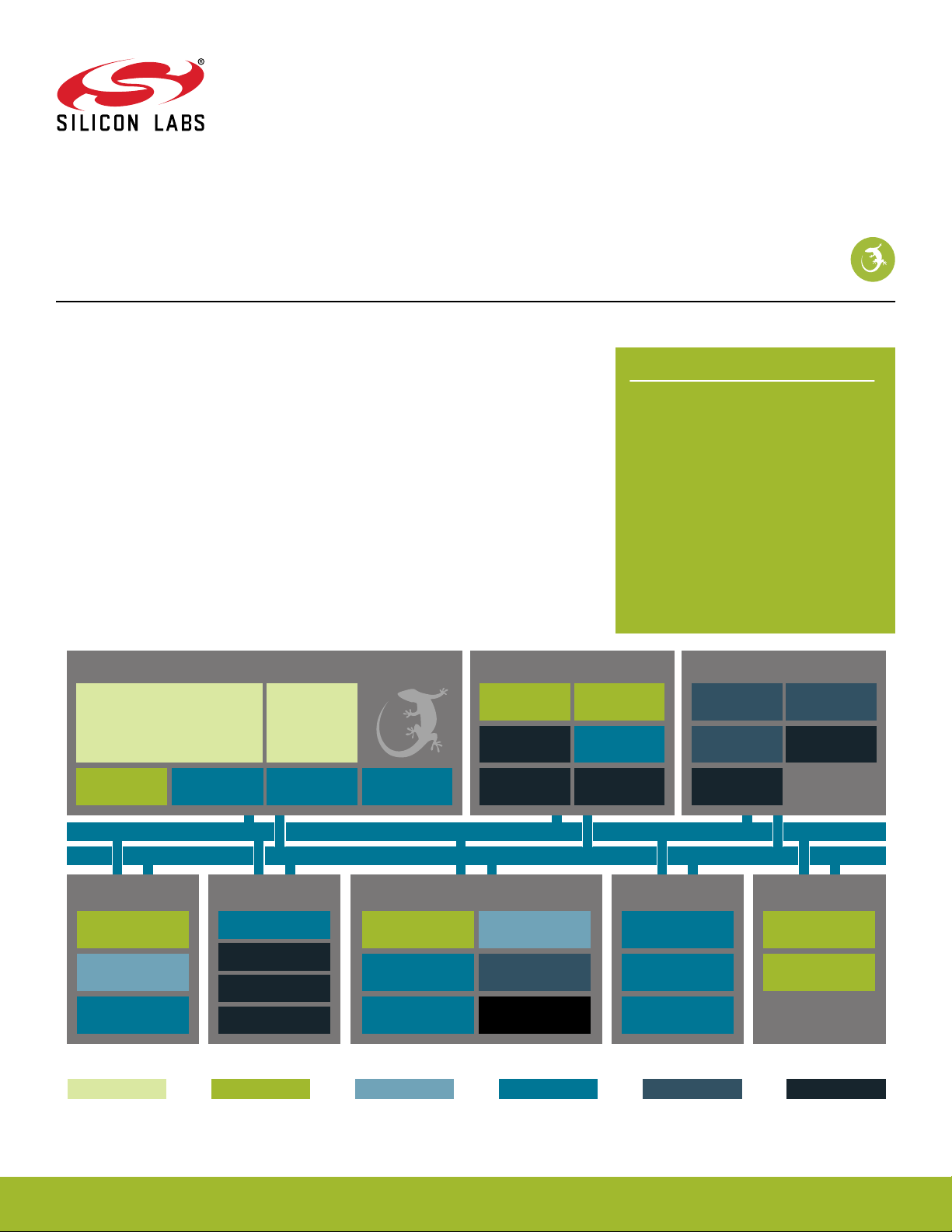
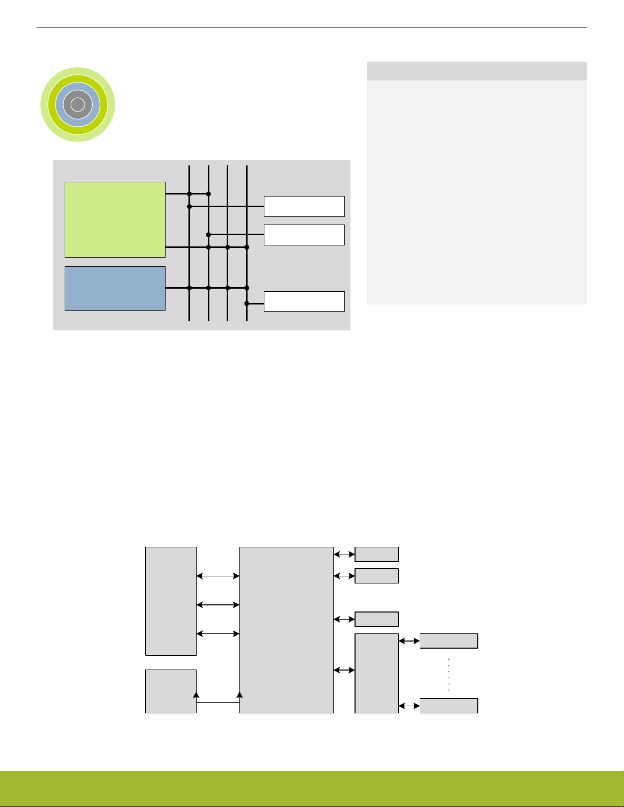
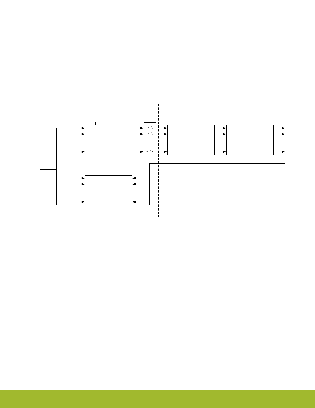
2.2 Block Diagrams
The block diagram for the EFM32 Jade Gecko MCU series is shown in (Figure 2.1 EFM32 Jade Gecko System-On-Chip Block Diagram
on page 5).
Core / Memory
ARM Cortex
Flash Program
Memory
TM
M3 processor
RAM Memory
Serial Interfaces
USART
Low Energy UART
I
TM
2
C
Lowest power mode with peripheral operational:
EM0 - Active
External Interrupts
General Purpose I/O
Pin Wakeup
EM1 - Sleep
Memory
Protection Unit
Debug Interface DMA Controller
I/O Ports Timers and Triggers
Pin Reset
Clock Management
High Frequency
Crystal
Oscillator
Low Frequency
RC Oscillator
Low Frequency
Crystal
Oscillator
32-bit bus
Peripheral Reflex System
Timer/Counter Low Energy Timer
Pulse Counter
Watchdog Timer
EM2 – Deep Sleep
Real Time Counter
and Calendar
CRYOTIMER
EM3 - Stop
High Frequency
RC Oscillator
Auxiliary High
Frequency RC
Oscillator
Ultra Low
Frequency RC
Oscillator
Analog Interfaces
Analog Comparator
Energy Management
Voltage
Regulator
Converter
Brown-Out
Detector
ADC
IDAC
EM4 - Hibernate
DC-DC
Voltage Monitor
Power-On Reset
Other
CRYPTO
CRC
EM4 - Shutoff
Figure 2.1. EFM32 Jade Gecko System-On-Chip Block Diagram
silabs.com | Smart. Connected. Energy-friendly. Preliminary Rev. 0.6 | 5
Page 7

EFM32JG1 Reference Manual
System Overview
2.3 MCU Features overview
• ARM Cortex-M3 CPU platform
• High Performance 32-bit processor @ up to 40 MHz
• Memory Protection Unit
• Wake-up Interrupt Controller
• Flexible Energy Management System
• Power routing configurations including DCDC control
• Voltage Monitoring and Brown Out Detection
• State Retention
• 256 KB Flash
• 32 KB RAM
• Up to 32 General Purpose I/O pins
• Configurable push-pull, open-drain, pull-up/down, input filter, drive strength
• Configurable peripheral I/O locations
• 16 asynchronous external interrupts
• Output state retention and wake-up from Shutoff Mode
• 8 Channel DMA Controller
• Alternate/primary descriptors with scatter-gather/ping-pong operation
• 12 Channel Peripheral Reflex System
• Autonomous inter-peripheral signaling enables smart operation in low energy modes
• CRYPTO Advanced Encryption Standard Accelerator
• AES encryption / decryption, with 128 or 256 bit keys
• Multiple AES modes of operation, including Counter (CTR), Galois/Counter Mode (GCM), Cipher Block Chaining (CBC), Cipher
Feedback (CFB) and Output Feedback (OFB).
• Accelerated SHA-1 and SHA-2
• Accelerated Elliptic Curve Cryptography (ECC), with binary or prime fields
• Flexible 256-bit ALU and sequencer
• General Purpose Cyclic Redundancy Check
• Programmable 16-bit polynomial, fixed 32-bit polynomial
• Communication interfaces
• 2×Universal Synchronous/Asynchronous Receiver/Transmitter
• UART/SPI/SmartCard (ISO 7816)/IrDA/I2S
• Triple buffered full/half-duplex operation
• Hardware flow control
• 4-16 data bits
• 1× Low Energy UART
• Autonomous operation with DMA in Deep Sleep Mode
•
1×I2C Interface with SMBus support
• Address recognition in Stop Mode
• Timers/Counters
• 2× 16-bit Timer/Counter
• 3 or 4 Compare/Capture/PWM channels
• Dead-Time Insertion on TIMER0
• 16-bit Low Energy Timer
• 32-bit Ultra Low Energy Timer/Counter (CRYOTIMER) for periodic wake-up from any Energy Mode
• 32-bit Real-Time Counter and Calendar
• 16+16+32 bit Protocol Timer
• 16-bit Pulse Counter
• Asynchronous pulse counting/quadrature decoding
• Watchdog Timer with dedicated RC oscillator @ 50 nA
• Ultra low power precision analog peripherals
• 12-bit 1 Msamples/s Analog to Digital Converter
• 8 input channels and on-chip temperature sensor
silabs.com | Smart. Connected. Energy-friendly. Preliminary Rev. 0.6 | 6
Page 8

EFM32JG1 Reference Manual
System Overview
• Single ended or differential operation
• Conversion tailgating for predictable latency
• Current Digital to Analog Converter
• Source or sink a configurable constant current
• 2× Analog Comparator
• Programmable speed/current
• Capacitive sensing with up to 8 inputs
• Analog Port
• Ultra efficient Power-on Reset and Brown-Out Detector
• Debug Interface
• 4-pin Joint Test Action Group (JTAG) interface
• 2-pin serial-wire debug (SWD) interface
2.4 Oscillators and Clocks
EFM32 Jade Gecko has six different oscillators integrated, as shown in Table 2.1 EFM32 Jade Gecko Oscillators on page 7
Table 2.1. EFM32 Jade Gecko Oscillators
Oscillator Frequency Optional? External
Description
components
HFXO 38 MHz - 40 MHz No Crystal High accuracy, low jitter high frequency crystal oscillator. Tun-
able crystal loading capacitors are fully integrated.
HFRCO 1 MHz - 38 MHz No - Medium accuracy RC oscillator, typically used for timing dur-
ing startup of the HFXO or if a precise oscillator is not required.
AUXHFRCO 1 MHz - 38 MHz No - Medium accuracy RC oscillator, typically used as alternative
clock source for Analog to Digital Converter or Debug Trace.
LFRCO 32768 Hz No - Medium accuracy frequency reference typically used for medi-
um accuracy RTCC timing.
LFXO 32768 Hz Yes Crystal High accuracy frequency reference typically used for high ac-
curacy RTCC timing. Tunable crystal loading capacitors are
fully integrated.
ULFRCO 1000 Hz No - Ultra low frequency oscillator typically used for the watchdog
timer.
The RC oscillators can be calibrated against either of the crystal oscillators in order to compensate for temperature and voltage supply
variations. Hardware support is included to measure the frequency of various oscillators against each other.
Oscillator and clock management is available through the Clock Management Unit (CMU), see section 10. CMU - Clock Management
Unit for details.
2.5 Hardware CRC Support
EFM32 Jade Gecko supports a configurable CRC generation:
• 8, 16, 24 or 32 bit CRC value
• Configurable polynomial and initialization value
• Optional inversion of CRC value over air
• Configurable CRC byte ordering
• Support for multiple CRC values calculated and verified per transmitted or received frame
silabs.com | Smart. Connected. Energy-friendly. Preliminary Rev. 0.6 | 7
Page 9

EFM32JG1 Reference Manual
System Overview
2.6 Data Encryption and Authentication
EFM32 Jade Gecko has hardware support for AES encryption, decryption and authentication modes. These security operations can be
performed on data in RAM or any data buffer, without further CPU intervention. The key size is 128 bits.
AES modes of operations directly supported by the EFM32 Jade Gecko hardware are listed in Table 2.2 AES modes of operation with
hardware support on page 8. In addition to these modes, other modes can also be implemented by using combinations of modes.
For example, the CCM mode can be implemented using the CTR and CBC-MAC modes in combination.
Table 2.2. AES modes of operation with hardware support
AES Mode Encryption / Decryption Authentication Comment
ECB Yes - Electronic Code Book
CTR Yes - Counter mode
CCM Yes Yes Counter with CBC-MAC
CCM* Yes Yes CCM with encryption-only and
integrity-only capabilities
GCM Yes Yes Galois Counter Mode
CBC Yes - Cipher Block Chaining
CBC-MAC - Yes Cipher Block Chaining, Mes-
sage Authentication Code
CMAC - Yes Cipher-basec MAC
CFB Yes - Cipher Feedback
OFB Yes - Output Feedback
The CRYPTO module can provide data directly from the embedded Cortex-M3 or via DMA.
silabs.com | Smart. Connected. Energy-friendly. Preliminary Rev. 0.6 | 8
Page 10

EFM32JG1 Reference Manual
System Overview
2.7 Timers
EFM32 Jade Gecko includes multiple timers, as can be seen from Table 2.3 EFM32 Jade Gecko Timers Overview on page 9.
Table 2.3. EFM32 Jade Gecko Timers Overview
Timer Number of instances Typical clock source Overview
RTCC 1 Low frequency (LFXO or
LFRCO)
32 bit Real Time Counter and
Calendar, typically used to accurately time inactive periods
and enable wakeup on compare
match.
TIMER 2 High frequency (HFXO or
16 bit general purpose timer.
HFRCO)
Systick timer 1 High frequency (HFXO or
HFRCO)
32 bit systick timer integrated in
the Cortex-M3. Typically used
as an Operating System timer.
WDOG 1 Low frequency (LFXO, LFRCO
or ULFRCO)
Watch dog timer. Once enabled,
this module must be periodically
accessed. If not, this is considered an error and the EFM32
Jade Gecko is reset in order to
recover the system.
LETIMER 1 Low frequency (LFXO, LFRCO
or ULFRCO)
Low energy general purpose
timer.
Advanced interconnect features allows synchronization between timers. This includes:
• Start / stop any high frequency timer synchronized with the RTCC
• Trigger RSM state transitions based on compare timer compare match, for instance to provide clock cycle accuracy on frame transmit timing
silabs.com | Smart. Connected. Energy-friendly. Preliminary Rev. 0.6 | 9
Page 11
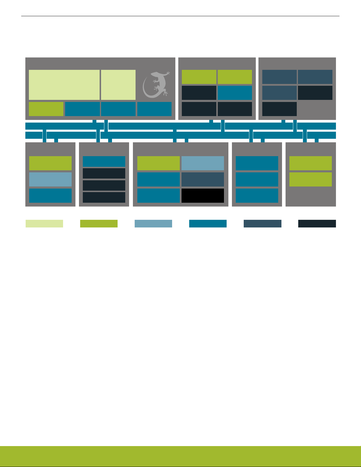
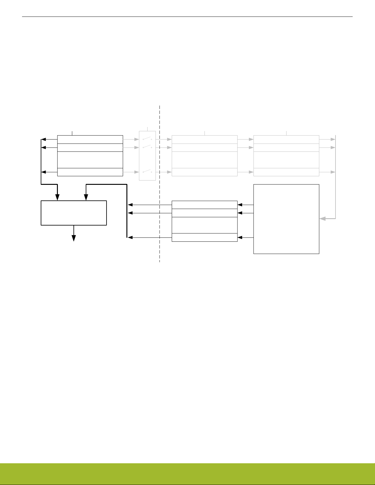
3. System Processor
0 1 2 3 4
CM3Core
Hardware divider
Control Logic
32-bit ALU
32-bit multiplier
Thumb & Thumb-2
Single cycle
Decode
EFM32JG1 Reference Manual
System Processor
Quick Facts
What?
The industry leading Cortex-M3 processor from
ARM is the CPU in the EFM32 Jade Gecko devices.
Why?
The ARM Cortex-M3 is designed for exceptionally
short response time, high code density, and high 32bit throughput while maintaining a strict cost and
power consumption budget.
How?
Combined with the ultra low energy peripherals
available in EFM32 Jade Gecko devices, the CortexM3 processor's Harvard architecture, 3 stage pipeline, single cycle instructions, Thumb-2 instruction
set support, and fast interrupt handling make it perfect for 8-bit, 16-bit, and 32-bit applications.
Instruction Interface Data Interface
NVIC Interface
Memory Protection Unit
3.1 Introduction
The ARM Cortex-M3 32-bit RISC processor provides outstanding computational performance and exceptional system response to interrupts while meeting low cost requirements and low power consumption.
The ARM Cortex-M3 implemented is revision r2p1.
silabs.com | Smart. Connected. Energy-friendly. Preliminary Rev. 0.6 | 10
Page 12

EFM32JG1 Reference Manual
System Processor
3.2 Features
• Harvard architecture
• Separate data and program memory buses (No memory bottleneck as in a single bus system)
• 3-stage pipeline
• Thumb-2 instruction set
• Enhanced levels of performance, energy efficiency, and code density
• Single cycle multiply and hardware divide instructions
• 32-bit multiplication in a single cycle
• Signed and unsigned divide operations between 2 and 12 cycles
• Atomic bit manipulation with bit banding
• Direct access to single bits of data
• Two 1MB bit banding regions for memory and peripherals mapping to 32MB alias regions
• Atomic operation, cannot be interrupted by other bus activities
• 1.25 DMIPS/MHz
• Memory Protection Unit
• Up to 8 protected memory regions
• 24 bits System Tick Timer for Real Time OS
• Excellent 32-bit migration choice for 8/16 bit architecture based designs
• Simplified stack-based programmer's model is compatible with traditional ARM architecture and retains the programming simplicity of legacy 8-bit and 16-bit architectures
• Alligned or unaligned data storage and access
• Contiguous storage of data requiring different byte lengths
• Data access in a single core access cycle
• Integrated power modes
• Sleep Now mode for immediate transfer to low power state
• Sleep on Exit mode for entry into low power state after the servicing of an interrupt
• Ability to extend power savings to other system components
• Optimized for low latency, nested interrupts
3.3 Functional Description
For a full functional description of the ARM Cortex-M3 implementation in the EFM32 Jade Gecko family, the reader is referred to the
ARM Cortex-M3 documentation.
silabs.com | Smart. Connected. Energy-friendly. Preliminary Rev. 0.6 | 11
Page 13
3.3.1 Interrupt Operation
Module Cortex-M4 NVIC
EFM32JG1 Reference Manual
System Processor
IFS[n] IFC[n]
IEN[n]
SETENA[n]/CLRENA[n]
Interrupt
condition
set clear
IF[n]
Active interrupt
IRQ
set clear
Interrupt
request
SETPEND[n]/CLRPEND[n]
Software generated interrupt
Figure 3.1. Interrupt Operation
The interrupt request (IRQ) lines are connected to the Cortex-M3. Each of these lines (shown in Table 3.1 Interrupt Request Lines (IRQ)
on page 13) is connected to one or more interrupt flags in one or more modules. The interrupt flags are set by hardware on an inter-
rupt condition. It is also possible to set/clear the interrupt flags through the IFS/IFC registers. Each interrupt flag is then qualified with its
own interrupt enable bit (IEN register), before being OR'ed with the other interrupt flags to generate the IRQ. A high IRQ line will set the
corresponding pending bit (can also be set/cleared with the SETPEND/CLRPEND bits in ISPR0/ICPR0) in the Cortex-M3 NVIC. The
pending bit is then qualified with an enable bit (set/cleared with SETENA/CLRENA bits in ISER0/ICER0) before generating an interrupt
request to the core. Figure 3.1 Interrupt Operation on page 12 illustrates the interrupt system. For more information on how the interrupts are handled inside the Cortex-M3, the reader is referred to the EFM32 Cortex-M3 Reference Manual.
3.3.1.1 Avoiding Extraneous Interrupts
There can be latencies in the system such that clearing an interrupt flag could take longer than leaving an Interrupt Service Routine
(ISR). This can lead to the ISR being re-entered as the interrupt flag has yet to clear immediately after leaving the ISR. To avoid this,
when clearing an interrupt flag at the end of an ISR, the user should execute ARM's Data Synchronization Barrier (DSB) instruction.
Another approach is to clear the interrupt flag immediately after identifying the interrupt source and then service the interrupt as shown
in the pseudo-code below. The ISR typically is sufficiently long to more than cover the few cycles it may take to clear the interrupt status, and also allows the status to be checked for further interrupts before exiting the ISR.
irqXServiceRoutine() {
do {
clearIrqXStatus();
serviceIrqX();
} while(irqXStatusIsActive());
}
3.3.1.2 IFC Read-clear Operation
In addition to the normal interrupt setting and clearing operations via the IFS/IFC registers, there is an additional atomic Read-clear
operation that can be enabled by setting IFCREADCLEAR=1 in the MSC_CTRL register. When enabled, reads of peripheral IFC registers will return the interrupt vector (mirroring the IF register), while at the same time clearing whichever interrupt flags are set. This operation is functionally equivalent to reading the IF register and then writing the result immediately back to the IFC register.
silabs.com | Smart. Connected. Energy-friendly. Preliminary Rev. 0.6 | 12
Page 14

3.3.2 Interrupt Request Lines (IRQ)
Table 3.1. Interrupt Request Lines (IRQ)
IRQ # Source
0 EMU
2 WDOG0
8 LDMA
9 GPIO_EVEN
10 TIMER0
11 USART0_RX
12 USART0_TX
13 ACMP0
14 ADC0
15 IDAC0
EFM32JG1 Reference Manual
System Processor
16 I2C0
17 GPIO_ODD
18 TIMER1
19 USART1_RX
20 USART1_TX
21 LEUART0
22 PCNT0
23 CMU
24 MSC
25 CRYPTO
26 LETIMER0
29 RTCC
31 CRYOTIMER
33 FPUEH
silabs.com | Smart. Connected. Energy-friendly. Preliminary Rev. 0.6 | 13
Page 15
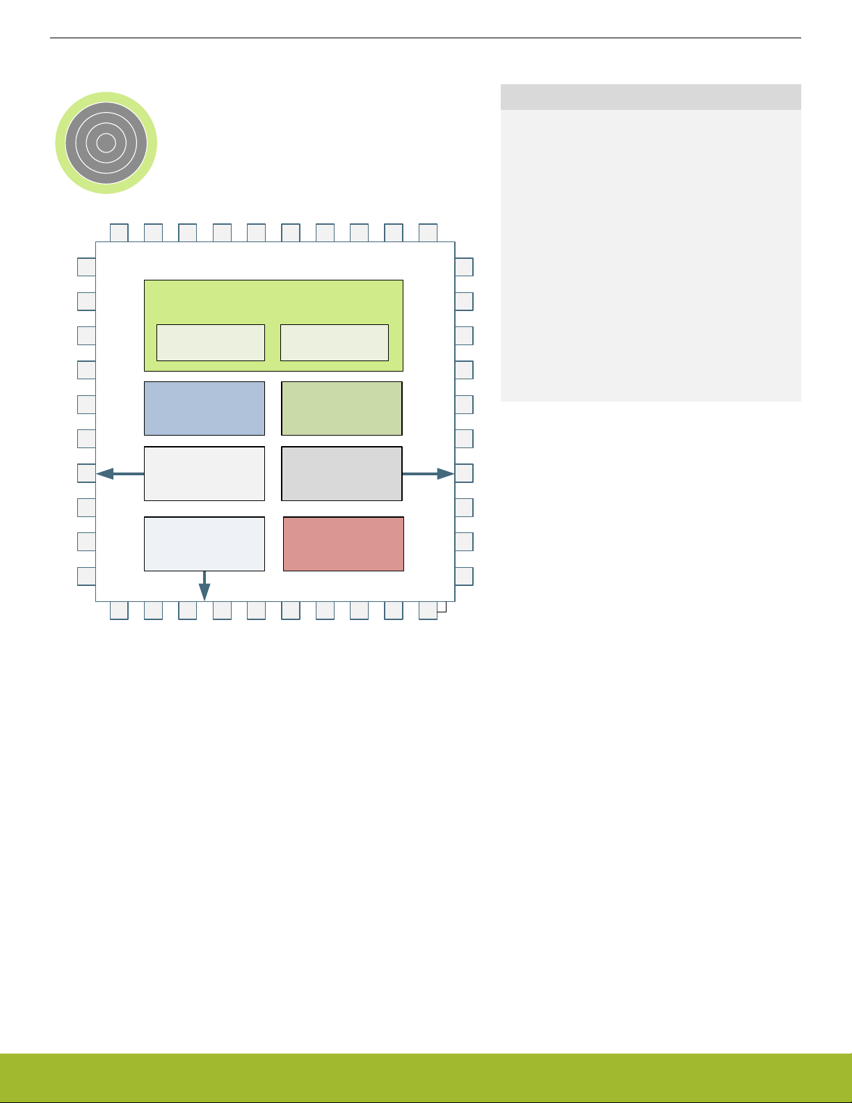
4. Memory and Bus System
0 1 2 3 4
ARM Cortex-M
DMA Controller
Flash
RAM
Peripherals
EFM32JG1 Reference Manual
Memory and Bus System
Quick Facts
What?
A low latency memory system including low energy
Flash and RAM with data retention which makes the
energy modes attractive.
Why?
RAM retention reduces the need for storing data in
Flash and enables frequent use of the ultra low energy modes EM2 DeepSleep and EM3 Stop.
How?
Low energy and non-volatile Flash memory stores
program and application data in all energy modes
and can easily be reprogrammed in system. Low
leakage RAM with data retention in EM0 Active to
EM3 Stop removes the data restore time penalty,
and the DMA ensures fast autonomous transfers
with predictable response time.
4.1 Introduction
The EFM32 Jade Gecko contains an AMBA AHB Bus system to allow bus masters to access the memory mapped address space. A
multilayer AHB bus matrix connects the 4 master bus interfaces to the AHB slaves (Figure 4.1 EFM32 Jade Gecko Bus System on
page 14). The bus matrix allows several AHB slaves to be accessed simultaneously. An AMBA APB interface is used for the peripher-
als, which are accessed through an AHB-to-APB bridge connected to the AHB bus matrix. The 4 AHB bus masters are:
• Cortex-M3 ICode: Used for instruction fetches from Code memory (valid address range: 0x00000000 - 0x1FFFFFFF)
• Cortex-M3 DCode: Used for debug and data access to Code memory (valid address range: 0x00000000 - 0x1FFFFFFF)
• Cortex-M3 System: Used for data and debug access to system space. It can access entire memory space except Code memory
(valid address range: 0x20000000 - 0xFFFFFFFF)
• DMA: Can access entire memory space except internal core memory region and Code memory (valid address range: 0x20000000 0xDFFFFFFF)
ARM
Cortex-M
DMA
ICode
DCode
System
AHB Multilayer
Bus Matrix
Flash
RAM
CRYPTO
AHB/
APB
Bridge
Peripheral 0
Peripheral n
Figure 4.1. EFM32 Jade Gecko Bus System
silabs.com | Smart. Connected. Energy-friendly. Preliminary Rev. 0.6 | 14
Page 16
EFM32JG1 Reference Manual
Memory and Bus System
4.2 Functional Description
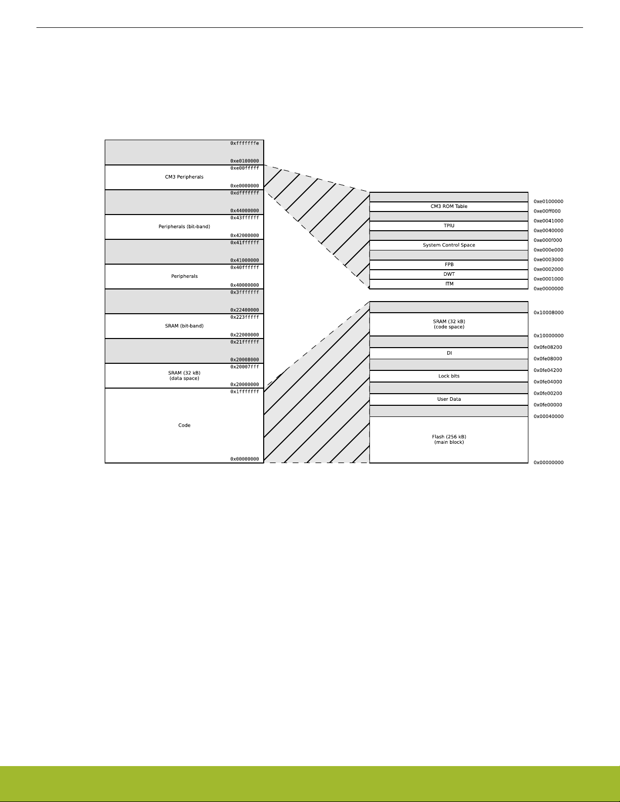
The memory segments are mapped together with the internal segments of the Cortex-M3 into the system memory map shown by Fig-
ure 4.2 System Address Space with Core and Code Space Listing on page 15.
Figure 4.2. System Address Space with Core and Code Space Listing
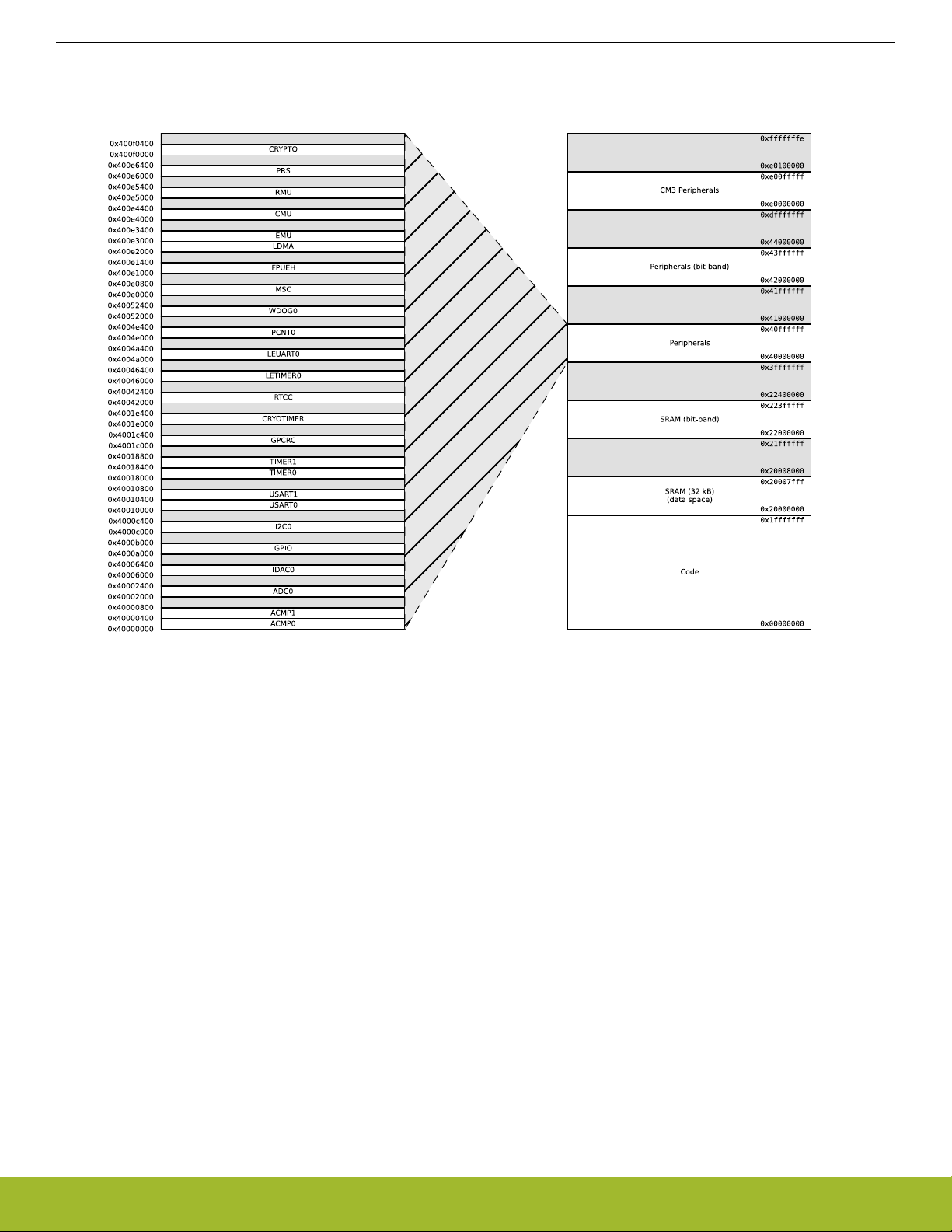
Additionally, the peripheral address map is detailed by Figure 4.3 System Address Space with Peripheral Listing on page 16.
silabs.com | Smart. Connected. Energy-friendly. Preliminary Rev. 0.6 | 15
Page 17
EFM32JG1 Reference Manual
Memory and Bus System
Figure 4.3. System Address Space with Peripheral Listing
The embedded SRAM is located at address 0x20000000 in the memory map of the EFM32 Jade Gecko. When running code located in
SRAM starting at this address, the Cortex-M3 uses the System bus interface to fetch instructions. This results in reduced performance
as the Cortex-M3 accesses stack, other data in SRAM and peripherals using the System bus interface. To be able to run code from
SRAM efficiently, the SRAM is also mapped in the code space at address 0x10000000. When running code from this space, the CortexM3 fetches instructions through the I/D-Code bus interface, leaving the System bus interface for data access. The SRAM mapped into
the code space can however only be accessed by the CPU, i.e. not the DMA.
silabs.com | Smart. Connected. Energy-friendly. Preliminary Rev. 0.6 | 16
Page 18

EFM32JG1 Reference Manual
Memory and Bus System
4.2.1 Bit-banding
The SRAM bit-band alias and peripheral bit-band alias regions are located at 0x22000000 and 0x42000000 respectively. Read and
write operations to these regions are converted into masked single-bit reads and atomic single-bit writes to the embedded SRAM and
peripherals of the EFM32 Jade Gecko.
Note: Bit-banding is only available through the CPU. No other AHB masters (e.g., DMA) can perform Bit-banding operations.
Using a standard approach to modify a single register or SRAM bit in the aliased regions, would require software to read the value of
the byte, half-word or word containing the bit, modify the bit, and then write the byte, half-word or word back to the register or SRAM
address. Using bit-banding, this can be done in a single operation, consuming only two bus cycles. As read-writeback, bit-masking and
bit-shift operations are not necessary in software, code size is reduced and execution speed improved.
The bit-band regions allow each bit in the SRAM and Peripheral areas of the memory map to be addressed. To set or clear a bit in the
embedded SRAM, write a 1 or a 0 to the following address:
bit_address = 0x22000000 + (address – 0x20000000) × 32 + bit × 4
where address is the address of the 32-bit word containing the bit to modify, and bit is the index of the bit in the 32-bit word.
To modify a bit in the Peripheral area, use the following address:
bit_address = 0x42000000 + (address – 0x40000000) × 32 + bit × 4
silabs.com | Smart. Connected. Energy-friendly. Preliminary Rev. 0.6 | 17
Page 19

EFM32JG1 Reference Manual
Memory and Bus System
4.2.2 Peripheral Bit Set and Clear
The EFM32 Jade Gecko supports bit set and bit clear access to all peripherals except those listed in Table 4.1 Peripherals that Do Not
Support Bit Set and Bit Clear on page 18. The bit set and bit clear functionality (also called Bit Access) enables modification of bit
fields (single bit or multiple bit wide) without the need to perform a read-modify-write (though it is functionally equivalent). Also, the operation is contained within a single bus access (for HF peripherals), unlike the Bit-banding operation described in section 4.2.1 Bit-
banding which consumes two bus accesses per operation. All AHB masters can utilize this feature.
The bit clear aliasing region starts at 0x44000000 and the bit set aliasing region starts at 0x46000000. Thus, to apply a bit set or clear
operation, write the bit set or clear mask to the following addresses:
bit_clear_address = address + 0x04000000
bit_set_address = address + 0x06000000
For bit set operations, bit locations that are 1 in the bit mask will be set in the destination register:
register = (register OR mask)
For bit clear operations, bit locations that are 1 in the bit mask will be cleared in the destination register:
register = (register AND (NOT mask))
Note: It is possible to combine bit clear and bit set operations in order to arbitrarily modify multi-bit register fields, without affecting other
fields in the same register. In this case, care should be taken to ensure that the field does not have intermediate values that can lead to
erroneous behavior. For example, if bit clear and bit set operations are used to change an analog tuning register field from 25 to 26, the
field would initially take on a value of zero. If the analog module is active at the time, this could lead to undesired behavior.
The peripherals listed in Table 4.1 Peripherals that Do Not Support Bit Set and Bit Clear on page 18 do not support Bit Access for any
registers. All other peripherals do support Bit Access, however, there may be cases of certain registers that do not support it. Such
registers have a note regarding this lack of support.
Table 4.1. Peripherals that Do Not Support Bit Set and Bit Clear
Module
EMU
RMU
CRYOTIMER
silabs.com | Smart. Connected. Energy-friendly. Preliminary Rev. 0.6 | 18
Page 20

EFM32JG1 Reference Manual
Memory and Bus System
4.2.3 Peripherals
The peripherals are mapped into the peripheral memory segment, each with a fixed size address range according to Table 4.2 Periph-
erals on page 19, Table 4.3 Low Energy Peripherals on page 19 , and Table 4.4 Core Peripherals on page 19.
Table 4.2. Peripherals
Address Range Module Name
0x400E6000 - 0x400E6400 PRS
0x4001E000 - 0x4001E400 CRYOTIMER
0x4001C000 - 0x4001C400 GPCRC
0x40018400 - 0x40018800 TIMER1
0x40018000 - 0x40018400 TIMER0
0x40010400 - 0x40010800 USART1
0x40010000 - 0x40010400 USART0
0x4000C000 - 0x4000C400 I2C0
0x4000A000 - 0x4000B000 GPIO
0x40006000 - 0x40006400 IDAC0
0x40002000 - 0x40002400 ADC0
0x40000400 - 0x40000800 ACMP1
0x40000000 - 0x40000400 ACMP0
Table 4.3. Low Energy Peripherals
Address Range Module Name
0x40052000 - 0x40052400 WDOG0
0x4004E000 - 0x4004E400 PCNT0
0x4004A000 - 0x4004A400 LEUART0
0x40046000 - 0x40046400 LETIMER0
0x40042000 - 0x40042400 RTCC
Table 4.4. Core Peripherals
Address Range Module Name
0x400F0000 - 0x400F0400 CRYPTO
0x400E2000 - 0x400E3000 LDMA
0x400E1000 - 0x400E1400 FPUEH
0x400E0000 - 0x400E0800 MSC
4.2.4 Bus Matrix
The Bus Matrix connects the memory segments to the bus masters as detailed in 4.1 Introduction.
silabs.com | Smart. Connected. Energy-friendly. Preliminary Rev. 0.6 | 19
Page 21

EFM32JG1 Reference Manual
Memory and Bus System
4.2.4.1 Arbitration
The Bus Matrix uses a round-robin arbitration algorithm which enables high throughput and low latency, while starvation of simultaneous accesses to the same bus slave are eliminated. Round-robin does not assign a fixed priority to each bus master. The arbiter does
not insert any bus wait-states during peak interaction. However, one wait state is inserted for master accesses occurring after a prolonged inactive time. This wait state allows for increased power efficiency during master idle time.
4.2.4.2 Access Performance
The Bus Matrix is a multi-layer energy optimized AMBA AHB compliant bus with an internal bandwidth of 4x a single AHB interface.
The Bus Matrix accepts new transfers to be initiated by each master in each cycle without inserting any wait-states. However, the
slaves may insert wait-states depending on their internal throughput and the clock frequency.
The Cortex-M3, DMA Controller, and peripherals (not peripherals in the low frequency clock domain) run on clocks which can be prescaled separately. Clocks and prescaling are described in more detail in 10. CMU - Clock Management Unit .
In general, when accessing a peripheral, the latency in number of HFBUSCLK cycles, not including master arbitration, is given by:
where N
slave cycles
N
bus cycles
N
bus cycles
N
bus cycles
N
bus cycles
is the number of cycles required to access the particular slave, including any wait cycles introduced by the slave.
= (N
= (N
= N
= N
slave cycles
slave cycles
slave cycles
slave cycles
+ 1) × f
+ 1) × f
× f
HFBUSCLK/fHFPERCLK
× f
HFBUSCLK/fHFPERCLK
HFBUSCLK/fHFPERCLK
HFBUSCLK/fHFPERCLK
, best-case write accesses
+ 1, best-case read accesses
- 1, worst-case write accesses
, worst-case read accesses
Figure 4.4. Bus Access Latency (General Case)
Note that a latency of 1 cycle corresponds to 0 wait states.
Additionally, for back-to-back accesses to the same peripheral, the throughput in number of cycles per transfer is given by:
N
bus cycles
N
bus cycles
= N
= (N
slave cycles
slave cycles
× f
HFBUSCLK/fHFPERCLK
+ 1) × f
HFBUSCLK/fHFPERCLK
, write accesses
, read accesses
Figure 4.5. Bus Access Throughput (Back-to-Back Transfers)
Lastly, in the highest performing case, where HFPERCLK equals HFBUSCLK and the slave doesn't introduce any additional wait
states, the access latency in number of cycles is given by:
N
bus cycles
= 1, write accesses
N
bus cycles
= 2, read accesses
Figure 4.6. Bus Access Latency (Max Performance)
Note that the cycle counts in the equations above is in terms of the HFBUSCLK. When the core is prescaled from the bus clock, the
core will see a reduced number of latency cycles given by:
N
core cycles
= ceiling( N
bus cycles
× f
HFCORECLK/fHFBUSCLK
)
where master arbitration is not included.
Figure 4.7. Core Access Latency
silabs.com | Smart. Connected. Energy-friendly. Preliminary Rev. 0.6 | 20
Page 22
EFM32JG1 Reference Manual
Memory and Bus System
4.2.4.3 Bus Faults
System accesses from the core can receive a bus fault in the following condition(s):
• The core attempts to access an address that is not assigned to any peripheral or other system device. These faults can be enabled
or disabled by setting the ADDRFAULTEN bit appropriately in MSC_CTRL.
• The core attempts to access a peripheral or system device that has its clock disabled. These faults can be enabled or disabled by
setting the CLKDISFAULTEN bit appropriately in MSC_CTRL.
In addition to any condition-specific bus fault control bits, the bus fault interrupt itself can be enabled or disabled in the same way as all
other internal core interrupts.
4.3 Access to Low Energy Peripherals (Asynchronous Registers)
The Low Energy Peripherals are capable of running when the high frequency oscillator and core system is powered off, i.e. in energy
mode EM2 DeepSleep and in some cases also EM3 Stop. This enables the peripherals to perform tasks while the system energy consumption is minimal.
The Low Energy Peripherals are listed in Table 4.3 Low Energy Peripherals on page 19.
All Low Energy Peripherals are memory mapped, with automatic data synchronization. Because the Low Energy Peripherals are running on clocks asynchronous to the high frequency system clock, there are some constraints on how register accesses are performed,
as described in the following sections.
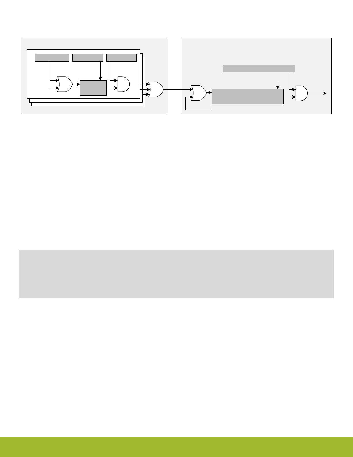
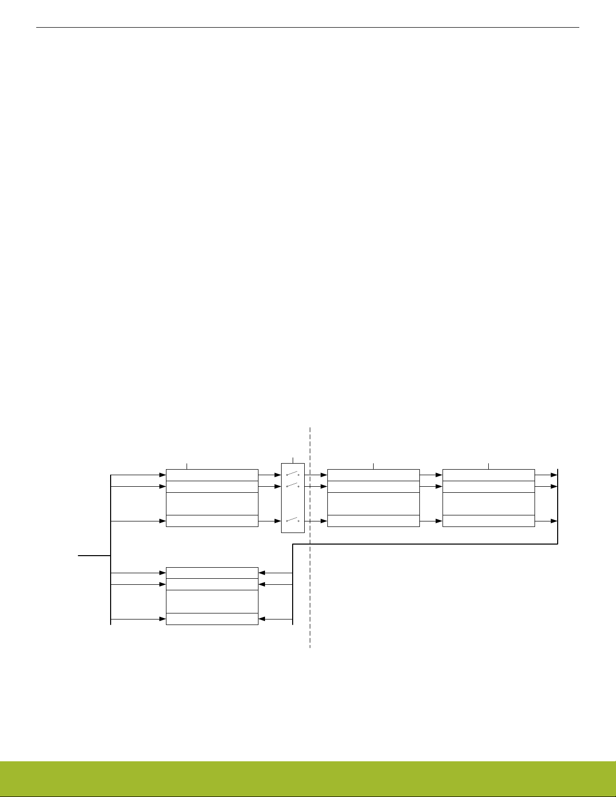
4.3.1 Writing
Every Low Energy Peripheral has one or more registers with data that needs to be synchronized into the Low Energy clock domain to
maintain data consistency and predictable operation. There are two different synchronization mechanisms on the EFM32JG1, immediate synchronization, and delayed synchronization. Immediate synchronization is available for the RTCC and LETIMER, and results in
an immediate update of the target registers. Delayed synchronization is used for the remaining Low Energy Peripherals, and for these
peripherals, a write operation requires 3 positive edges of the clock on the Low Energy Peripheral being accessed. Registers requiring
synchronization are marked "Async Reg" in their description header.
Note: On the Gecko series of devices, all LE peripherals are subject to delayed synchronization.
Write request [0:n]
High Frequency Clock Domain
High Frequency Clock
Write request 0
Write request 1
Write request n
Set 0
Set 1
Set n
Register 0
Register 1
.
.
.
Register n
Syncbusy Register 0
Syncbusy Register 1
.
.
.
Syncbusy Register n
Freeze
Clear 0
Clear 1
Clear n
Low Frequency Clock Domain
Low Frequency Clock Low Frequency Clock
Synchronizer 0
Synchronizer 1
.
.
.
Synchronizer n
Synchronization Done
Register 0 Sync
Register 1 Sync
Register n Sync
.
.
.
Figure 4.8. Write operation to Low Energy Peripherals
silabs.com | Smart. Connected. Energy-friendly. Preliminary Rev. 0.6 | 21
Page 23
EFM32JG1 Reference Manual
Memory and Bus System
4.3.1.1 Delayed Synchronization
After writing data to a register which value is to be synchronized into the Low Energy Peripheral using delayed synchronization, a corresponding busy flag in the <module_name>_SYNCBUSY register (e.g. LETIMER_SYNCBUSY) is set. This flag is set as long as synchronization is in progress and is cleared upon completion.
Note: Subsequent writes to the same register before the corresponding busy flag is cleared is not supported. Write before the busy flag
is cleared may result in undefined behavior. In general the SYNCBUSY register only needs to be observed if there is a risk of multiple
write access to a register (which must be prevented). It is not required to wait until the relevant flag in the SYNCBUSY register is
cleared after writing a register. E.g., EM2 DeepSleep can be entered directly after writing a register.
See Figure 4.9 Write operation to Low Energy Peripherals on page 22 for an overview of the writing mechanism operation.
Write request [0:n]
High Frequency Clock Domain
High Frequency Clock
Write request 0
Write request 1
Write request n
Set 0
Set 1
Set n
Register 0
Register 1
.
.
.
Register n
Syncbusy Register 0
Syncbusy Register 1
.
.
.
Syncbusy Register n
Freeze
Clear 0
Clear 1
Clear n
Low Frequency Clock Domain
Low Frequency Clock Low Frequency Clock
Synchronizer 0
Synchronizer 1
.
.
.
Synchronizer n
Synchronization Done
Register 0 Sync
Register 1 Sync
Register n Sync
.
.
.
Figure 4.9. Write operation to Low Energy Peripherals
4.3.1.2 Immediate Synchronization
In contrast to the peripherals with delayed synchronization, peripherals with immediate synchronization don't experience a delay from a
value is written to it takes effect in the peripheral. They are updated immediately on the peripheral write access. If such a write is done
close to an edge on the clock of the peripheral, the write is delayed to after the clock edge. This will introduce wait-states on the peripheral access.
Peripherals with immediate synchronization each have a SYNCBUSY register. Commands written to a peripheral with immediate synchronization are not executed before the first peripheral clock after the write. In this period, the SYNCBUSY flag for the command register is set, indicating that the command has not yet been performed. Secondly, to maintain compatibility with the Gecko series, the rest
of the SYNCBUSY registers are also present, but these are always 0, indicating that register writes are always safe.
Note: If compatibility with the Gecko series is a requirement for a given application, the rules that apply to delayed synchronization with
respect to SYNCBUSY should also be followed for the peripherals that support immediate synchronization.
silabs.com | Smart. Connected. Energy-friendly. Preliminary Rev. 0.6 | 22
Page 24
EFM32JG1 Reference Manual
Memory and Bus System
4.3.2 Reading
When reading from a Low Energy Peripheral, the data read is synchronized regardless if it originates in the Low Energy clock domain
or High Frequency clock domain. See Figure 4.10 Read operation from Low Energy Peripherals on page 23 for an overview of the
reading operation.
Note: Writing a register and then immediately reading the new value of the register may give the impression that the write operation is
complete. This may not be the case. Please refer to the SYNCBUSY register for correct status of the write operation to the Low Energy
Peripheral.
High Frequency Clock Domain Low Frequency Clock Domain
High Frequency Clock
Freeze
Low Frequency Clock Low Frequency Clock
Register 0
Register 1
.
.
.
Register n
Read
Synchronizer
Read Data
Synchronizer 0
Synchronizer 1
.
.
.
Synchronizer n
HW Status Register 0
HW Status Register 1
.
.
.
HW Status Register m
Register 0 Sync
Register 1 Sync
.
.
.
Register n Sync
Low Energy
Peripheral
Main
Function
Figure 4.10. Read operation from Low Energy Peripherals
4.3.3 FREEZE Register
In all Low Energy Peripheral with delayed synchronization there is a <module_name>_FREEZE register (e.g. RTCC_FREEZE). The
register contains a bit named REGFREEZE. If precise control of the synchronization process is required, this bit may be utilized. When
REGFREEZE is set, the synchronization process is halted allowing the software to write multiple Low Energy registers before starting
the synchronization process, thus providing precise control of the module update process. The synchronization process is started by
clearing the REGFREEZE bit.
Note: The FREEZE register is also present on peripherals with immediate synchronization, but there it has no effect
4.4 Flash
The Flash retains data in any state and typically stores the application code, special user data and security information. The Flash
memory is typically programmed through the debug interface, but can also be erased and written to from software.
• Up to 256 KB of memory
• Page size of 2048 bytes (minimum erase unit)
• Minimum 10K erase cycles endurance
• Greater than 10 years data retention at 85°C
• Lock-bits for memory protection
• Data retention in any state
silabs.com | Smart. Connected. Energy-friendly. Preliminary Rev. 0.6 | 23
Page 25

EFM32JG1 Reference Manual
Memory and Bus System
4.5 SRAM
The primary task of the SRAM memory is to store application data. Additionally, it is possible to execute instructions from SRAM, and
the DMA may be set up to transfer data between the SRAM, Flash and peripherals.
• Up to 32 KB of memory
• Bit-band access support
• Set of RAM blocks may be powered down when not in use
• Data retention of the entire memory in EM0 Active to EM3 Stop
The SRAM memory may be split among two or more different AHB slaves (e.g., RAM0, RAM1, ...) in order to allow simultaneous access to different sections of the memory from two different AHB masters. For example, the Cortex-M3 can access RAM0 while the DMA
controller accesses RAM1 in parallel. See Figure 4.1 EFM32 Jade Gecko Bus System on page 14 for AHB slave connectivity details.
silabs.com | Smart. Connected. Energy-friendly. Preliminary Rev. 0.6 | 24
Page 26

EFM32JG1 Reference Manual
Memory and Bus System
4.6 DI Page Entry Map
The DI page contains production calibration data as well as device identification information. See the peripheral chapters for how each
calibration value is to be used with the associated peripheral.
The offset address is relative to the start address of the DI page.(see 6.3 Functional Description)
Offset Name Type Description
0x000 CAL RO CRC of DI-page and calibration temperature
0x028 EUI48L RO EUI48 OUI and Unique identifier
0x02C EUI48H RO OUI
0x030 CUSTOMINFO RO Custom information
0x034 MEMINFO RO Flash page size and misc. chip information
0x040 UNIQUEL RO Low 32 bits of device unique number
0x044 UNIQUEH RO High 32 bits of device unique number
0x048 MSIZE RO Flash and SRAM Memory size in kB
0x04C PART RO Part description
0x050 DEVINFOREV RO Device information page revision
0x054 EMUTEMP RO EMU Temperature Calibration Information
0x060 ADC0CAL0 RO ADC0 calibration register 0
0x064 ADC0CAL1 RO ADC0 calibration register 1
0x068 ADC0CAL2 RO ADC0 calibration register 2
0x06C ADC0CAL3 RO ADC0 calibration register 3
0x080 HFRCOCAL0 RO HFRCO Calibration Register (4 MHz)
0x08C HFRCOCAL3 RO HFRCO Calibration Register (7 MHz)
0x098 HFRCOCAL6 RO HFRCO Calibration Register (13 MHz)
0x09C HFRCOCAL7 RO HFRCO Calibration Register (16 MHz)
0x0A0 HFRCOCAL8 RO HFRCO Calibration Register (19 MHz)
0x0A8 HFRCOCAL10 RO HFRCO Calibration Register (26 MHz)
0x0AC HFRCOCAL11 RO HFRCO Calibration Register (32 MHz)
0x0B0 HFRCOCAL12 RO HFRCO Calibration Register (38 MHz)
0x0E0 AUXHFRCOCAL0 RO AUXHFRCO Calibration Register (4 MHz)
0x0EC AUXHFRCOCAL3 RO AUXHFRCO Calibration Register (7 MHz)
0x0F8 AUXHFRCOCAL6 RO AUXHFRCO Calibration Register (13 MHz)
0x0FC AUXHFRCOCAL7 RO AUXHFRCO Calibration Register (16 MHz)
0x100 AUXHFRCOCAL8 RO AUXHFRCO Calibration Register (19 MHz)
0x108 AUXHFRCOCAL10 RO AUXHFRCO Calibration Register (26 MHz)
0x10C AUXHFRCOCAL11 RO AUXHFRCO Calibration Register (32 MHz)
0x110 AUXHFRCOCAL12 RO AUXHFRCO Calibration Register (38 MHz)
0x140 VMONCAL0 RO VMON Calibration Register 0
0x144 VMONCAL1 RO VMON Calibration Register 1
0x148 VMONCAL2 RO VMON Calibration Register 2
silabs.com | Smart. Connected. Energy-friendly. Preliminary Rev. 0.6 | 25
Page 27
Offset Name Type Description
0x158 IDAC0CAL0 RO IDAC0 Calibration Register 0
0x15C IDAC0CAL1 RO IDAC0 Calibration Register 1
0x168 DCDCLNVCTRL0 RO DCDC Low-noise VREF Trim Register 0
0x16C DCDCLPVCTRL0 RO DCDC Low-power VREF Trim Register 0
0x170 DCDCLPVCTRL1 RO DCDC Low-power VREF Trim Register 1
0x174 DCDCLPVCTRL2 RO DCDC Low-power VREF Trim Register 2
0x178 DCDCLPVCTRL3 RO DCDC Low-power VREF Trim Register 3
0x17C DCDCLPCMPHYSSEL0 RO DCDC LPCMPHYSSEL Trim Register 0
0x180 DCDCLPCMPHYSSEL1 RO DCDC LPCMPHYSSEL Trim Register 1
4.7 DI Page Entry Description
4.7.1 CAL - CRC of DI-page and calibration temperature
Offset Bit Position
EFM32JG1 Reference Manual
Memory and Bus System
0x000
Access
31
30
29
28
27
26
25
24
23
22
21
20
RO
19
18
17
16
15
14
13
12
11
10
9
8
7
6
5
RO
Name
TEMP
CRC
Bit Name Access Description
31:24 Reserved Reserved for future use
23:16 TEMP RO Calibration temperature as an usigned int in DegC
(25 = 25DegC)
15:0 CRC RO CRC of DI-page (CRC-16-CCITT)
4
3
2
1
0
silabs.com | Smart. Connected. Energy-friendly. Preliminary Rev. 0.6 | 26
Page 28
4.7.2 EUI48L - EUI48 OUI and Unique identifier
Offset Bit Position
EFM32JG1 Reference Manual
Memory and Bus System
0x028
Access
31
30
29
28
RO
27
26
25
24
23
22
21
20
19
18
17
16
15
14
13
12
11
RO
10
9
8
7
6
5
4
Name
OUI48L
UNIQUEID
Bit Name Access Description
31:24 OUI48L RO Lower Octet of EUI48 Organizationally Unique Identi-
fier
23:0 UNIQUEID RO Unique identifier
4.7.3 EUI48H - OUI
Offset Bit Position
0x02C
Access
31
30
29
28
27
26
25
24
23
22
21
20
19
18
17
16
15
14
13
12
11
10
9
8
7
6
5
4
RO
3
2
1
0
3
2
1
0
Name
OUI48H
Bit Name Access Description
31:16 Reserved Reserved for future use
15:0 OUI48H RO Upper two Octets of EUI48 Organizationally Unique
Identifier
4.7.4 CUSTOMINFO - Custom information
Offset Bit Position
0x030
Access
31
30
29
28
27
26
25
24
RO
23
22
21
20
19
18
17
16
15
14
13
12
11
10
9
8
7
6
5
Name
PARTNO
Bit Name Access Description
31:16 PARTNO RO Custom part identifier as unsigned integer (e.g. 903)
65535 for standard product
4
3
2
1
0
15:0 Reserved Reserved for future use
silabs.com | Smart. Connected. Energy-friendly. Preliminary Rev. 0.6 | 27
Page 29

4.7.5 MEMINFO - Flash page size and misc. chip information
Offset Bit Position
EFM32JG1 Reference Manual
Memory and Bus System
0x034
Access
31
30
29
28
RO
27
26
25
24
23
22
21
20
RO
19
18
17
16
15
14
13
12
11
RO
10
9
8
7
Name
FLASH_PAGE_SIZE
PINCOUNT
PKGTYPE
Bit Name Access Description
31:24 FLASH_PAGE_SIZE RO Flash page size in bytes coded as 2 ^ ((MEM_IN-
FO_PAGE_SIZE + 10) & 0xFF). Ie. the value 0xFF
= 512 bytes.
23:16 PINCOUNT RO Device pin count as unsigned integer (eg. 48)
15:8 PKGTYPE RO Package Identifier as character
Value Mode Description
6
5
4
3
2
1
0
RO
TEMPGRADE
74 WLCSP WLCSP package
77 QFN QFN package
81 QFP QFP package
7:0 TEMPGRADE RO Temperature Grade of product as unsigned inte-
ger enumeration
Value Mode Description
0 N40TO85 -40 to 85degC
1 N40TO125 -40 to 125degC
2 N40TO105 -40 to 105degC
3 N0TO70 0 to 70degC
silabs.com | Smart. Connected. Energy-friendly. Preliminary Rev. 0.6 | 28
Page 30
4.7.6 UNIQUEL - Low 32 bits of device unique number
Offset Bit Position
EFM32JG1 Reference Manual
Memory and Bus System
0x040
Access
31
30
29
28
27
26
25
24
23
22
21
20
19
18
17
16
RO
15
14
13
12
11
10
9
Name
UNIQUEL
Bit Name Access Description
31:0 UNIQUEL RO Low 32 bits of device unique number
4.7.7 UNIQUEH - High 32 bits of device unique number
Offset Bit Position
0x044
Access
31
30
29
28
27
26
25
24
23
22
21
20
19
18
17
16
RO
15
14
13
12
11
10
9
Name
UNIQUEH
8
7
6
5
4
3
2
1
0
8
7
6
5
4
3
2
1
0
Bit Name Access Description
31:0 UNIQUEH RO High 32 bits of device unique number
4.7.8 MSIZE - Flash and SRAM Memory size in kB
Offset Bit Position
0x048
Access
31
30
29
28
27
26
25
24
RO
23
22
21
20
19
18
17
16
15
14
13
12
11
10
9
8
7
6
5
RO
Name
SRAM
FLASH
Bit Name Access Description
31:16 SRAM RO Ram size, kbyte count as unsigned integer (eg. 16)
15:0 FLASH RO Flash size, kbyte count as unsigned integer (eg. 128)
4
3
2
1
0
silabs.com | Smart. Connected. Energy-friendly. Preliminary Rev. 0.6 | 29
Page 31

4.7.9 PART - Part description
Offset Bit Position
EFM32JG1 Reference Manual
Memory and Bus System
0x04C
Access
31
30
29
28
RO
27
26
25
24
23
22
21
20
RO
19
18
17
16
15
14
13
12
11
10
9
Name
PROD_REV
DEVICE_FAMILY
Bit Name Access Description
31:24 PROD_REV RO Production revision as unsigned integer
23:16 DEVICE_FAMILY RO Device Family
Value Mode Description
16 EFR32MG1P EFR32 Mighty Gecko Gen1 Device Family
17 EFR32MG1B EFR32 Mighty Gecko Gen1 Device Family
18 EFR32MG1V EFR32 Mighty Gecko Gen1 Device Family
8
7
6
5
RO
DEVICE_NUMBER
4
3
2
1
0
19 EFR32BG1P EFR32 Blue Gecko Gen1 Device Family
20 EFR32BG1B EFR32 Blue Gecko Gen1 Device Family
21 EFR32BG1V EFR32 Blue Gecko Gen1 Device Family
25 EFR32FG1P EFR32 Flex Gecko Gen1 Device Family
26 EFR32FG1B EFR32 Flex Gecko Gen1 Device Family
27 EFR32FG1V EFR32 Flex Gecko Gen1 Device Family
71 EFM32G EFM32 Gecko Device Family
71 G EFM32 Gecko Device Family
72 EFM32GG EFM32 Giant Gecko Device Family
72 GG EFM32 Giant Gecko Device Family
73 TG EFM32 Tiny Gecko Device Family
73 EFM32TG EFM32 Tiny Gecko Device Family
74 EFM32LG EFM32 Leopard Gecko Device Family
74 LG EFM32 Leopard Gecko Device Family
75 EFM32WG EFM32 Wonder Gecko Device Family
75 WG EFM32 Wonder Gecko Device Family
76 ZG EFM32 Zero Gecko Device Family
76 EFM32ZG EFM32 Zero Gecko Device Family
77 HG EFM32 Happy Gecko Device Family
77 EFM32HG EFM32 Happy Gecko Device Family
silabs.com | Smart. Connected. Energy-friendly. Preliminary Rev. 0.6 | 30
Page 32

Bit Name Access Description
81 EFM32PG1B EFM32 Pearl Gecko Gen1 Device Family
83 EFM32JG1B EFM32 Jade Gecko Gen1 Device Family
120 EZR32LG EZR32 Leopard Gecko Device Family
121 EZR32WG EZR32 Wonder Gecko Device Family
122 EZR32HG EZR32 Happy Gecko Device Family
15:0 DEVICE_NUMBER RO Part number as unsigned integer (e.g. 233 for
EFR32BG1P233F256GM48-B0)
4.7.10 DEVINFOREV - Device information page revision
Offset Bit Position
EFM32JG1 Reference Manual
Memory and Bus System
0x050
31
30
29
28
27
26
25
24
23
22
21
20
19
18
17
16
15
14
13
12
11
10
9
8
7
6
5
4
Access
Name
Bit Name Access Description
31:8 Reserved Reserved for future use
7:0 DEVINFOREV RO DEVINFO layout revision as unsigned integer (initial-
ly 1)
4.7.11 EMUTEMP - EMU Temperature Calibration Information
Offset Bit Position
0x054
31
30
29
28
27
26
25
24
23
22
21
20
19
18
17
16
15
14
13
12
11
10
9
8
7
6
5
4
Access
3
2
1
RO
DEVINFOREV
3
2
1
RO
0
0
Name
EMUTEMPROOM
Bit Name Access Description
31:8 Reserved Reserved for future use
7:0 EMUTEMPROOM RO EMU_TEMP temperature reading at room
silabs.com | Smart. Connected. Energy-friendly. Preliminary Rev. 0.6 | 31
Page 33

4.7.12 ADC0CAL0 - ADC0 calibration register 0
Offset Bit Position
EFM32JG1 Reference Manual
Memory and Bus System
0x060
Access
31
30
29
28
27
RO
26
25
24
23
22
RO
21
20
19
18
RO
17
16
15
14
13
12
11
RO
10
9
8
7
6
RO
Name
GAIN2V5
NEGSEOFFSET2V5
OFFSET2V5
GAIN1V25
NEGSEOFFSET1V25
Bit Name Access Description
31 Reserved Reserved for future use
30:24 GAIN2V5 RO Gain for 2.5V reference
23:20 NEGSEOFFSET2V5 RO Negative single ended offset for 2.5V reference
19:16 OFFSET2V5 RO Offset for 2.5V reference
15 Reserved Reserved for future use
5
4
3
2
1
0
RO
OFFSET1V25
14:8 GAIN1V25 RO Gain for 1.25V reference
7:4 NEGSEOFFSET1V25 RO Negative single ended offset for 1.25V reference
3:0 OFFSET1V25 RO Offset for 1.25V reference
silabs.com | Smart. Connected. Energy-friendly. Preliminary Rev. 0.6 | 32
Page 34

4.7.13 ADC0CAL1 - ADC0 calibration register 1
Offset Bit Position
EFM32JG1 Reference Manual
Memory and Bus System
0x064
Access
31
30
29
28
27
RO
26
25
24
23
22
RO
21
20
19
18
RO
17
16
15
14
13
12
11
RO
10
9
8
7
6
5
RO
Name
GAIN5VDIFF
NEGSEOFFSET5VDIFF
OFFSET5VDIFF
GAINVDD
NEGSEOFFSETVDD
Bit Name Access Description
31 Reserved Reserved for future use
30:24 GAIN5VDIFF RO Gain for for 5V differential reference
23:20 NEGSEOFFSET5VDIFF RO Negative single ended offset with for 5V differential
reference
19:16 OFFSET5VDIFF RO Offset for 5V differential reference
4
3
2
1
0
RO
OFFSETVDD
15 Reserved Reserved for future use
14:8 GAINVDD RO Gain for VDD reference
7:4 NEGSEOFFSETVDD RO Negative single ended offset for VDD reference
3:0 OFFSETVDD RO Offset for VDD reference
silabs.com | Smart. Connected. Energy-friendly. Preliminary Rev. 0.6 | 33
Page 35

4.7.14 ADC0CAL2 - ADC0 calibration register 2
Offset Bit Position
EFM32JG1 Reference Manual
Memory and Bus System
0x068
Access
31
30
29
28
27
26
25
24
23
22
21
20
19
18
17
16
15
14
13
12
11
10
9
8
7
6
5
RO
Name
NEGSEOFFSET2XVDD
Bit Name Access Description
31 Reserved Reserved for future use
30:24 Reserved Reserved for future use
23:20 Reserved Reserved for future use
19:16 Reserved Reserved for future use
15:8 Reserved Reserved for future use
7:4 NEGSEOFFSET2XVDD RO Negative single ended offset for 2XVDD reference
4
3
2
1
0
RO
OFFSET2XVDD
3:0 OFFSET2XVDD RO Offset for 2XVDD reference
4.7.15 ADC0CAL3 - ADC0 calibration register 3
Offset Bit Position
0x06C
Access
31
30
29
28
27
26
25
24
23
22
21
20
19
18
17
16
15
14
13
12
11
10
RO
9
8
Name
TEMPREAD1V25
Bit Name Access Description
31:16 Reserved Reserved for future use
15:4 TEMPREAD1V25 RO Temperature reading at 1V25 reference
3:0 Reserved Reserved for future use
7
6
5
4
3
2
1
0
silabs.com | Smart. Connected. Energy-friendly. Preliminary Rev. 0.6 | 34
Page 36

4.7.16 HFRCOCAL0 - HFRCO Calibration Register (4 MHz)
Offset Bit Position
EFM32JG1 Reference Manual
Memory and Bus System
0x080
Access
31
30
RO
29
28
27
RO
26
RO
25
24
RO
23
22
RO
21
20
19
18
RO
17
16
15
14
13
12
11
RO
10
9
8
7
6
5
4
Name
VREFTC
FINETUNINGEN
CLKDIV
LDOHP
CMPBIAS
FREQRANGE
FINETUNING
Bit Name Access Description
31:28 VREFTC RO HFRCO Temperature Coefficient Trim on Comparator
Reference
27 FINETUNINGEN RO HFRCO enable reference for fine tuning
26:25 CLKDIV RO HFRCO Clock Output Divide
24 LDOHP RO HFRCO LDO High Power Mode
3
2
RO
TUNING
1
0
23:21 CMPBIAS RO HFRCO Comparator Bias Current
20:16 FREQRANGE RO HFRCO Frequency Range
15:14 Reserved Reserved for future use
13:8 FINETUNING RO HFRCO Fine Tuning Value
7 Reserved Reserved for future use
6:0 TUNING RO HFRCO Tuning Value
silabs.com | Smart. Connected. Energy-friendly. Preliminary Rev. 0.6 | 35
Page 37

4.7.17 HFRCOCAL3 - HFRCO Calibration Register (7 MHz)
Offset Bit Position
EFM32JG1 Reference Manual
Memory and Bus System
0x08C
Access
31
30
RO
29
28
27
RO
26
RO
25
24
RO
23
22
RO
21
20
19
18
RO
17
16
15
14
13
12
11
RO
10
9
8
7
6
5
4
Name
VREFTC
FINETUNINGEN
CLKDIV
LDOHP
CMPBIAS
FREQRANGE
FINETUNING
Bit Name Access Description
31:28 VREFTC RO HFRCO Temperature Coefficient Trim on Comparator
Reference
27 FINETUNINGEN RO HFRCO enable reference for fine tuning
26:25 CLKDIV RO HFRCO Clock Output Divide
24 LDOHP RO HFRCO LDO High Power Mode
3
2
RO
TUNING
1
0
23:21 CMPBIAS RO HFRCO Comparator Bias Current
20:16 FREQRANGE RO HFRCO Frequency Range
15:14 Reserved Reserved for future use
13:8 FINETUNING RO HFRCO Fine Tuning Value
7 Reserved Reserved for future use
6:0 TUNING RO HFRCO Tuning Value
silabs.com | Smart. Connected. Energy-friendly. Preliminary Rev. 0.6 | 36
Page 38

4.7.18 HFRCOCAL6 - HFRCO Calibration Register (13 MHz)
Offset Bit Position
EFM32JG1 Reference Manual
Memory and Bus System
0x098
Access
31
30
RO
29
28
27
RO
26
RO
25
24
RO
23
22
RO
21
20
19
18
RO
17
16
15
14
13
12
11
RO
10
9
8
7
6
5
4
Name
VREFTC
FINETUNINGEN
CLKDIV
LDOHP
CMPBIAS
FREQRANGE
FINETUNING
Bit Name Access Description
31:28 VREFTC RO HFRCO Temperature Coefficient Trim on Comparator
Reference
27 FINETUNINGEN RO HFRCO enable reference for fine tuning
26:25 CLKDIV RO HFRCO Clock Output Divide
24 LDOHP RO HFRCO LDO High Power Mode
3
2
RO
TUNING
1
0
23:21 CMPBIAS RO HFRCO Comparator Bias Current
20:16 FREQRANGE RO HFRCO Frequency Range
15:14 Reserved Reserved for future use
13:8 FINETUNING RO HFRCO Fine Tuning Value
7 Reserved Reserved for future use
6:0 TUNING RO HFRCO Tuning Value
silabs.com | Smart. Connected. Energy-friendly. Preliminary Rev. 0.6 | 37
Page 39

4.7.19 HFRCOCAL7 - HFRCO Calibration Register (16 MHz)
Offset Bit Position
EFM32JG1 Reference Manual
Memory and Bus System
0x09C
Access
31
30
RO
29
28
27
RO
26
RO
25
24
RO
23
22
RO
21
20
19
18
RO
17
16
15
14
13
12
11
RO
10
9
8
7
6
5
4
Name
VREFTC
FINETUNINGEN
CLKDIV
LDOHP
CMPBIAS
FREQRANGE
FINETUNING
Bit Name Access Description
31:28 VREFTC RO HFRCO Temperature Coefficient Trim on Comparator
Reference
27 FINETUNINGEN RO HFRCO enable reference for fine tuning
26:25 CLKDIV RO HFRCO Clock Output Divide
24 LDOHP RO HFRCO LDO High Power Mode
3
2
RO
TUNING
1
0
23:21 CMPBIAS RO HFRCO Comparator Bias Current
20:16 FREQRANGE RO HFRCO Frequency Range
15:14 Reserved Reserved for future use
13:8 FINETUNING RO HFRCO Fine Tuning Value
7 Reserved Reserved for future use
6:0 TUNING RO HFRCO Tuning Value
silabs.com | Smart. Connected. Energy-friendly. Preliminary Rev. 0.6 | 38
Page 40

4.7.20 HFRCOCAL8 - HFRCO Calibration Register (19 MHz)
Offset Bit Position
EFM32JG1 Reference Manual
Memory and Bus System
0x0A0
Access
31
30
RO
29
28
27
RO
26
RO
25
24
RO
23
22
RO
21
20
19
18
RO
17
16
15
14
13
12
11
RO
10
9
8
7
6
5
4
Name
VREFTC
FINETUNINGEN
CLKDIV
LDOHP
CMPBIAS
FREQRANGE
FINETUNING
Bit Name Access Description
31:28 VREFTC RO HFRCO Temperature Coefficient Trim on Comparator
Reference
27 FINETUNINGEN RO HFRCO enable reference for fine tuning
26:25 CLKDIV RO HFRCO Clock Output Divide
24 LDOHP RO HFRCO LDO High Power Mode
3
2
RO
TUNING
1
0
23:21 CMPBIAS RO HFRCO Comparator Bias Current
20:16 FREQRANGE RO HFRCO Frequency Range
15:14 Reserved Reserved for future use
13:8 FINETUNING RO HFRCO Fine Tuning Value
7 Reserved Reserved for future use
6:0 TUNING RO HFRCO Tuning Value
silabs.com | Smart. Connected. Energy-friendly. Preliminary Rev. 0.6 | 39
Page 41

4.7.21 HFRCOCAL10 - HFRCO Calibration Register (26 MHz)
Offset Bit Position
EFM32JG1 Reference Manual
Memory and Bus System
0x0A8
Access
31
30
RO
29
28
27
RO
26
RO
25
24
RO
23
22
RO
21
20
19
18
RO
17
16
15
14
13
12
11
RO
10
9
8
7
6
5
4
Name
VREFTC
FINETUNINGEN
CLKDIV
LDOHP
CMPBIAS
FREQRANGE
FINETUNING
Bit Name Access Description
31:28 VREFTC RO HFRCO Temperature Coefficient Trim on Comparator
Reference
27 FINETUNINGEN RO HFRCO enable reference for fine tuning
26:25 CLKDIV RO HFRCO Clock Output Divide
24 LDOHP RO HFRCO LDO High Power Mode
3
2
RO
TUNING
1
0
23:21 CMPBIAS RO HFRCO Comparator Bias Current
20:16 FREQRANGE RO HFRCO Frequency Range
15:14 Reserved Reserved for future use
13:8 FINETUNING RO HFRCO Fine Tuning Value
7 Reserved Reserved for future use
6:0 TUNING RO HFRCO Tuning Value
silabs.com | Smart. Connected. Energy-friendly. Preliminary Rev. 0.6 | 40
Page 42

4.7.22 HFRCOCAL11 - HFRCO Calibration Register (32 MHz)
Offset Bit Position
EFM32JG1 Reference Manual
Memory and Bus System
0x0AC
Access
31
30
RO
29
28
27
RO
26
RO
25
24
RO
23
22
RO
21
20
19
18
RO
17
16
15
14
13
12
11
RO
10
9
8
7
6
5
4
Name
VREFTC
FINETUNINGEN
CLKDIV
LDOHP
CMPBIAS
FREQRANGE
FINETUNING
Bit Name Access Description
31:28 VREFTC RO HFRCO Temperature Coefficient Trim on Comparator
Reference
27 FINETUNINGEN RO HFRCO enable reference for fine tuning
26:25 CLKDIV RO HFRCO Clock Output Divide
24 LDOHP RO HFRCO LDO High Power Mode
3
2
RO
TUNING
1
0
23:21 CMPBIAS RO HFRCO Comparator Bias Current
20:16 FREQRANGE RO HFRCO Frequency Range
15:14 Reserved Reserved for future use
13:8 FINETUNING RO HFRCO Fine Tuning Value
7 Reserved Reserved for future use
6:0 TUNING RO HFRCO Tuning Value
silabs.com | Smart. Connected. Energy-friendly. Preliminary Rev. 0.6 | 41
Page 43

4.7.23 HFRCOCAL12 - HFRCO Calibration Register (38 MHz)
Offset Bit Position
EFM32JG1 Reference Manual
Memory and Bus System
0x0B0
Access
31
30
RO
29
28
27
RO
26
RO
25
24
RO
23
22
RO
21
20
19
18
RO
17
16
15
14
13
12
11
RO
10
9
8
7
6
5
4
Name
VREFTC
FINETUNINGEN
CLKDIV
LDOHP
CMPBIAS
FREQRANGE
FINETUNING
Bit Name Access Description
31:28 VREFTC RO HFRCO Temperature Coefficient Trim on Comparator
Reference
27 FINETUNINGEN RO HFRCO enable reference for fine tuning
26:25 CLKDIV RO HFRCO Clock Output Divide
24 LDOHP RO HFRCO LDO High Power Mode
3
2
RO
TUNING
1
0
23:21 CMPBIAS RO HFRCO Comparator Bias Current
20:16 FREQRANGE RO HFRCO Frequency Range
15:14 Reserved Reserved for future use
13:8 FINETUNING RO HFRCO Fine Tuning Value
7 Reserved Reserved for future use
6:0 TUNING RO HFRCO Tuning Value
silabs.com | Smart. Connected. Energy-friendly. Preliminary Rev. 0.6 | 42
Page 44

4.7.24 AUXHFRCOCAL0 - AUXHFRCO Calibration Register (4 MHz)
Offset Bit Position
EFM32JG1 Reference Manual
Memory and Bus System
0x0E0
Access
31
30
RO
29
28
27
RO
26
RO
25
24
RO
23
22
RO
21
20
19
18
RO
17
16
15
14
13
12
11
RO
10
9
8
7
6
5
4
Name
VREFTC
FINETUNINGEN
CLKDIV
LDOHP
CMPBIAS
FREQRANGE
FINETUNING
Bit Name Access Description
31:28 VREFTC RO AUXHFRCO Temperature Coefficient Trim on Compa-
rator Reference
27 FINETUNINGEN RO AUXHFRCO enable reference for fine tuning
26:25 CLKDIV RO AUXHFRCO Clock Output Divide
24 LDOHP RO AUXHFRCO LDO High Power Mode
3
2
RO
TUNING
1
0
23:21 CMPBIAS RO AUXHFRCO Comparator Bias Current
20:16 FREQRANGE RO AUXHFRCO Frequency Range
15:14 Reserved Reserved for future use
13:8 FINETUNING RO AUXHFRCO Fine Tuning Value
7 Reserved Reserved for future use
6:0 TUNING RO AUXHFRCO Tuning Value
silabs.com | Smart. Connected. Energy-friendly. Preliminary Rev. 0.6 | 43
Page 45

4.7.25 AUXHFRCOCAL3 - AUXHFRCO Calibration Register (7 MHz)
Offset Bit Position
EFM32JG1 Reference Manual
Memory and Bus System
0x0EC
Access
31
30
RO
29
28
27
RO
26
RO
25
24
RO
23
22
RO
21
20
19
18
RO
17
16
15
14
13
12
11
RO
10
9
8
7
6
5
4
Name
VREFTC
FINETUNINGEN
CLKDIV
LDOHP
CMPBIAS
FREQRANGE
FINETUNING
Bit Name Access Description
31:28 VREFTC RO AUXHFRCO Temperature Coefficient Trim on Compa-
rator Reference
27 FINETUNINGEN RO AUXHFRCO enable reference for fine tuning
26:25 CLKDIV RO AUXHFRCO Clock Output Divide
24 LDOHP RO AUXHFRCO LDO High Power Mode
3
2
RO
TUNING
1
0
23:21 CMPBIAS RO AUXHFRCO Comparator Bias Current
20:16 FREQRANGE RO AUXHFRCO Frequency Range
15:14 Reserved Reserved for future use
13:8 FINETUNING RO AUXHFRCO Fine Tuning Value
7 Reserved Reserved for future use
6:0 TUNING RO AUXHFRCO Tuning Value
silabs.com | Smart. Connected. Energy-friendly. Preliminary Rev. 0.6 | 44
Page 46

4.7.26 AUXHFRCOCAL6 - AUXHFRCO Calibration Register (13 MHz)
Offset Bit Position
EFM32JG1 Reference Manual
Memory and Bus System
0x0F8
Access
31
30
RO
29
28
27
RO
26
RO
25
24
RO
23
22
RO
21
20
19
18
RO
17
16
15
14
13
12
11
RO
10
9
8
7
6
5
4
Name
VREFTC
FINETUNINGEN
CLKDIV
LDOHP
CMPBIAS
FREQRANGE
FINETUNING
Bit Name Access Description
31:28 VREFTC RO AUXHFRCO Temperature Coefficient Trim on Compa-
rator Reference
27 FINETUNINGEN RO AUXHFRCO enable reference for fine tuning
26:25 CLKDIV RO AUXHFRCO Clock Output Divide
24 LDOHP RO AUXHFRCO LDO High Power Mode
3
2
RO
TUNING
1
0
23:21 CMPBIAS RO AUXHFRCO Comparator Bias Current
20:16 FREQRANGE RO AUXHFRCO Frequency Range
15:14 Reserved Reserved for future use
13:8 FINETUNING RO AUXHFRCO Fine Tuning Value
7 Reserved Reserved for future use
6:0 TUNING RO AUXHFRCO Tuning Value
silabs.com | Smart. Connected. Energy-friendly. Preliminary Rev. 0.6 | 45
Page 47

4.7.27 AUXHFRCOCAL7 - AUXHFRCO Calibration Register (16 MHz)
Offset Bit Position
EFM32JG1 Reference Manual
Memory and Bus System
0x0FC
Access
31
30
RO
29
28
27
RO
26
RO
25
24
RO
23
22
RO
21
20
19
18
RO
17
16
15
14
13
12
11
RO
10
9
8
7
6
5
4
Name
VREFTC
FINETUNINGEN
CLKDIV
LDOHP
CMPBIAS
FREQRANGE
FINETUNING
Bit Name Access Description
31:28 VREFTC RO AUXHFRCO Temperature Coefficient Trim on Compa-
rator Reference
27 FINETUNINGEN RO AUXHFRCO enable reference for fine tuning
26:25 CLKDIV RO AUXHFRCO Clock Output Divide
24 LDOHP RO AUXHFRCO LDO High Power Mode
3
2
RO
TUNING
1
0
23:21 CMPBIAS RO AUXHFRCO Comparator Bias Current
20:16 FREQRANGE RO AUXHFRCO Frequency Range
15:14 Reserved Reserved for future use
13:8 FINETUNING RO AUXHFRCO Fine Tuning Value
7 Reserved Reserved for future use
6:0 TUNING RO AUXHFRCO Tuning Value
silabs.com | Smart. Connected. Energy-friendly. Preliminary Rev. 0.6 | 46
Page 48

4.7.28 AUXHFRCOCAL8 - AUXHFRCO Calibration Register (19 MHz)
Offset Bit Position
EFM32JG1 Reference Manual
Memory and Bus System
0x100
Access
31
30
RO
29
28
27
RO
26
RO
25
24
RO
23
22
RO
21
20
19
18
RO
17
16
15
14
13
12
11
RO
10
9
8
7
6
5
4
Name
VREFTC
FINETUNINGEN
CLKDIV
LDOHP
CMPBIAS
FREQRANGE
FINETUNING
Bit Name Access Description
31:28 VREFTC RO AUXHFRCO Temperature Coefficient Trim on Compa-
rator Reference
27 FINETUNINGEN RO AUXHFRCO enable reference for fine tuning
26:25 CLKDIV RO AUXHFRCO Clock Output Divide
24 LDOHP RO AUXHFRCO LDO High Power Mode
3
2
RO
TUNING
1
0
23:21 CMPBIAS RO AUXHFRCO Comparator Bias Current
20:16 FREQRANGE RO AUXHFRCO Frequency Range
15:14 Reserved Reserved for future use
13:8 FINETUNING RO AUXHFRCO Fine Tuning Value
7 Reserved Reserved for future use
6:0 TUNING RO AUXHFRCO Tuning Value
silabs.com | Smart. Connected. Energy-friendly. Preliminary Rev. 0.6 | 47
Page 49

4.7.29 AUXHFRCOCAL10 - AUXHFRCO Calibration Register (26 MHz)
Offset Bit Position
EFM32JG1 Reference Manual
Memory and Bus System
0x108
Access
31
30
RO
29
28
27
RO
26
RO
25
24
RO
23
22
RO
21
20
19
18
RO
17
16
15
14
13
12
11
RO
10
9
8
7
6
5
4
Name
VREFTC
FINETUNINGEN
CLKDIV
LDOHP
CMPBIAS
FREQRANGE
FINETUNING
Bit Name Access Description
31:28 VREFTC RO AUXHFRCO Temperature Coefficient Trim on Compa-
rator Reference
27 FINETUNINGEN RO AUXHFRCO enable reference for fine tuning
26:25 CLKDIV RO AUXHFRCO Clock Output Divide
24 LDOHP RO AUXHFRCO LDO High Power Mode
3
2
RO
TUNING
1
0
23:21 CMPBIAS RO AUXHFRCO Comparator Bias Current
20:16 FREQRANGE RO AUXHFRCO Frequency Range
15:14 Reserved Reserved for future use
13:8 FINETUNING RO AUXHFRCO Fine Tuning Value
7 Reserved Reserved for future use
6:0 TUNING RO AUXHFRCO Tuning Value
silabs.com | Smart. Connected. Energy-friendly. Preliminary Rev. 0.6 | 48
Page 50

4.7.30 AUXHFRCOCAL11 - AUXHFRCO Calibration Register (32 MHz)
Offset Bit Position
EFM32JG1 Reference Manual
Memory and Bus System
0x10C
Access
31
30
RO
29
28
27
RO
26
RO
25
24
RO
23
22
RO
21
20
19
18
RO
17
16
15
14
13
12
11
RO
10
9
8
7
6
5
4
Name
VREFTC
FINETUNINGEN
CLKDIV
LDOHP
CMPBIAS
FREQRANGE
FINETUNING
Bit Name Access Description
31:28 VREFTC RO AUXHFRCO Temperature Coefficient Trim on Compa-
rator Reference
27 FINETUNINGEN RO AUXHFRCO enable reference for fine tuning
26:25 CLKDIV RO AUXHFRCO Clock Output Divide
24 LDOHP RO AUXHFRCO LDO High Power Mode
3
2
RO
TUNING
1
0
23:21 CMPBIAS RO AUXHFRCO Comparator Bias Current
20:16 FREQRANGE RO AUXHFRCO Frequency Range
15:14 Reserved Reserved for future use
13:8 FINETUNING RO AUXHFRCO Fine Tuning Value
7 Reserved Reserved for future use
6:0 TUNING RO AUXHFRCO Tuning Value
silabs.com | Smart. Connected. Energy-friendly. Preliminary Rev. 0.6 | 49
Page 51

4.7.31 AUXHFRCOCAL12 - AUXHFRCO Calibration Register (38 MHz)
Offset Bit Position
EFM32JG1 Reference Manual
Memory and Bus System
0x110
Access
31
30
RO
29
28
27
RO
26
RO
25
24
RO
23
22
RO
21
20
19
18
RO
17
16
15
14
13
12
11
RO
10
9
8
7
6
5
4
Name
VREFTC
FINETUNINGEN
CLKDIV
LDOHP
CMPBIAS
FREQRANGE
FINETUNING
Bit Name Access Description
31:28 VREFTC RO AUXHFRCO Temperature Coefficient Trim on Compa-
rator Reference
27 FINETUNINGEN RO AUXHFRCO enable reference for fine tuning
26:25 CLKDIV RO AUXHFRCO Clock Output Divide
24 LDOHP RO AUXHFRCO LDO High Power Mode
3
2
RO
TUNING
1
0
23:21 CMPBIAS RO AUXHFRCO Comparator Bias Current
20:16 FREQRANGE RO AUXHFRCO Frequency Range
15:14 Reserved Reserved for future use
13:8 FINETUNING RO AUXHFRCO Fine Tuning Value
7 Reserved Reserved for future use
6:0 TUNING RO AUXHFRCO Tuning Value
silabs.com | Smart. Connected. Energy-friendly. Preliminary Rev. 0.6 | 50
Page 52

4.7.32 VMONCAL0 - VMON Calibration Register 0
Offset Bit Position
EFM32JG1 Reference Manual
Memory and Bus System
0x140
Access
31
30
RO
29
28
27
26
RO
25
24
23
22
RO
21
20
19
18
RO
17
16
15
14
RO
13
12
11
10
RO
9
8
7
Name
ALTAVDD2V98THRESCOARSE
ALTAVDD2V98THRESFINE
ALTAVDD1V86THRESCOARSE
ALTAVDD1V86THRESFINE
AVDD2V98THRESCOARSE
AVDD2V98THRESFINE
Bit Name Access Description
31:28 ALTAVDD2V98THRESCOARSE RO ALTAVDD 2.98 V Coarse Threshold Adjust
27:24 ALTAVDD2V98THRESFINE RO ALTAVDD 2.98 V Fine Threshold Adjust
23:20 ALTAVDD1V86THRESCOARSE RO ALTAVDD 1.86 V Coarse Threshold Adjust
6
5
4
3
2
1
RO
AVDD1V86THRESCOARSE
RO
AVDD1V86THRESFINE
0
19:16 ALTAVDD1V86THRESFINE RO ALTAVDD 1.86 V Fine Threshold Adjust
15:12 AVDD2V98THRESCOARSE RO AVDD 2.98 V Coarse Threshold Adjust
11:8 AVDD2V98THRESFINE RO AVDD 2.98 V Fine Threshold Adjust
7:4 AVDD1V86THRESCOARSE RO AVDD 1.86 V Coarse Threshold Adjust
3:0 AVDD1V86THRESFINE RO AVDD 1.86 V Fine Threshold Adjust
silabs.com | Smart. Connected. Energy-friendly. Preliminary Rev. 0.6 | 51
Page 53

4.7.33 VMONCAL1 - VMON Calibration Register 1
Offset Bit Position
EFM32JG1 Reference Manual
Memory and Bus System
0x144
Access
31
30
RO
29
28
27
26
RO
25
24
23
22
RO
21
20
19
18
RO
17
16
15
14
RO
13
12
11
10
9
RO
Name
IO02V98THRESCOARSE
IO02V98THRESFINE
IO01V86THRESCOARSE
IO01V86THRESFINE
DVDD2V98THRESCOARSE
DVDD2V98THRESFINE
Bit Name Access Description
31:28 IO02V98THRESCOARSE RO IO0 2.98 V Coarse Threshold Adjust
27:24 IO02V98THRESFINE RO IO0 2.98 V Fine Threshold Adjust
23:20 IO01V86THRESCOARSE RO IO0 1.86 V Coarse Threshold Adjust
8
7
6
5
4
3
2
1
0
RO
DVDD1V86THRESCOARSE
RO
DVDD1V86THRESFINE
19:16 IO01V86THRESFINE RO IO0 1.86 V Fine Threshold Adjust
15:12 DVDD2V98THRESCOARSE RO DVDD 2.98 V Coarse Threshold Adjust
11:8 DVDD2V98THRESFINE RO DVDD 2.98 V Fine Threshold Adjust
7:4 DVDD1V86THRESCOARSE RO DVDD 1.86 V Coarse Threshold Adjust
3:0 DVDD1V86THRESFINE RO DVDD 1.86 V Fine Threshold Adjust
silabs.com | Smart. Connected. Energy-friendly. Preliminary Rev. 0.6 | 52
Page 54

4.7.34 VMONCAL2 - VMON Calibration Register 2
Offset Bit Position
EFM32JG1 Reference Manual
Memory and Bus System
0x148
Access
31
30
RO
29
28
27
26
RO
25
24
23
22
RO
21
20
19
18
RO
17
16
15
14
RO
13
12
11
10
RO
9
8
Name
FVDD2V98THRESCOARSE
FVDD2V98THRESFINE
FVDD1V86THRESCOARSE
FVDD1V86THRESFINE
PAVDD2V98THRESCOARSE
PAVDD2V98THRESFINE
Bit Name Access Description
31:28 FVDD2V98THRESCOARSE RO FVDD 2.98 V Coarse Threshold Adjust
27:24 FVDD2V98THRESFINE RO FVDD 2.98 V Fine Threshold Adjust
23:20 FVDD1V86THRESCOARSE RO FVDD 1.86 V Coarse Threshold Adjust
7
6
5
4
3
2
RO
PAVDD1V86THRESCOARSE
1
0
RO
PAVDD1V86THRESFINE
19:16 FVDD1V86THRESFINE RO FVDD 1.86 V Fine Threshold Adjust
15:12 PAVDD2V98THRESCOARSE RO PAVDD 2.98 V Coarse Threshold Adjust
11:8 PAVDD2V98THRESFINE RO PAVDD 2.98 V Fine Threshold Adjust
7:4 PAVDD1V86THRESCOARSE RO PAVDD 1.86 V Coarse Threshold Adjust
3:0 PAVDD1V86THRESFINE RO PAVDD 1.86 V Fine Threshold Adjust
silabs.com | Smart. Connected. Energy-friendly. Preliminary Rev. 0.6 | 53
Page 55

4.7.35 IDAC0CAL0 - IDAC0 Calibration Register 0
Offset Bit Position
EFM32JG1 Reference Manual
Memory and Bus System
0x158
Access
31
30
29
28
RO
27
26
25
24
23
22
21
20
RO
19
18
17
16
15
14
13
12
11
RO
10
9
8
7
6
5
Name
SOURCERANGE3TUNING
SOURCERANGE2TUNING
SOURCERANGE1TUNING
Bit Name Access Description
31:24 SOURCERANGE3TUNING RO Calibrated middle step (16) of current source mode
range 3
23:16 SOURCERANGE2TUNING RO Calibrated middle step (16) of current source mode
range 2
15:8 SOURCERANGE1TUNING RO Calibrated middle step (16) of current source mode
range 1
4
3
2
1
0
RO
SOURCERANGE0TUNING
7:0 SOURCERANGE0TUNING RO Calibrated middle step (16) of current source mode
range 0
silabs.com | Smart. Connected. Energy-friendly. Preliminary Rev. 0.6 | 54
Page 56

4.7.36 IDAC0CAL1 - IDAC0 Calibration Register 1
Offset Bit Position
EFM32JG1 Reference Manual
Memory and Bus System
0x15C
Access
31
30
29
28
RO
27
26
25
24
23
22
21
20
RO
19
18
17
16
15
14
13
12
11
RO
10
9
8
7
6
5
Name
SINKRANGE3TUNING
SINKRANGE2TUNING
SINKRANGE1TUNING
Bit Name Access Description
31:24 SINKRANGE3TUNING RO Calibrated middle step (16) of current sink mode
range 3
23:16 SINKRANGE2TUNING RO Calibrated middle step (16) of current sink mode
range 2
15:8 SINKRANGE1TUNING RO Calibrated middle step (16) of current sink mode
range 1
4
3
2
1
0
RO
SINKRANGE0TUNING
7:0 SINKRANGE0TUNING RO Calibrated middle step (16) of current sink mode
range 0
4.7.37 DCDCLNVCTRL0 - DCDC Low-noise VREF Trim Register 0
Offset Bit Position
0x168
Access
31
30
29
28
RO
27
26
25
24
23
22
21
20
RO
19
18
17
16
15
14
13
12
11
RO
10
9
8
7
6
Name
3V0LNATT1
1V8LNATT1
1V8LNATT0
Bit Name Access Description
31:24 3V0LNATT1 RO DCDC LNVREF Trim for 3.0V output, LNATT=1
23:16 1V8LNATT1 RO DCDC LNVREF Trim for 1.8V output, LNATT=1
5
4
3
2
1
0
RO
1V2LNATT0
15:8 1V8LNATT0 RO DCDC LNVREF Trim for 1.8V output, LNATT=0
7:0 1V2LNATT0 RO DCDC LNVREF Trim for 1.2V output, LNATT=0
silabs.com | Smart. Connected. Energy-friendly. Preliminary Rev. 0.6 | 55
Page 57

4.7.38 DCDCLPVCTRL0 - DCDC Low-power VREF Trim Register 0
Offset Bit Position
EFM32JG1 Reference Manual
Memory and Bus System
0x16C
Access
31
30
29
28
RO
27
26
25
24
23
22
21
20
RO
19
18
17
16
15
14
13
12
11
RO
10
9
8
7
6
Name
1V8LPATT0LPCMPBIAS1
1V2LPATT0LPCMPBIAS1
1V8LPATT0LPCMPBIAS0
Bit Name Access Description
31:24 1V8LPATT0LPCMPBIAS1 RO DCDC LPVREF Trim for 1.8V output, LPATT=0,
LPCMPBIAS=1
23:16 1V2LPATT0LPCMPBIAS1 RO DCDC LPVREF Trim for 1.2V output, LPATT=0,
LPCMPBIAS=1
15:8 1V8LPATT0LPCMPBIAS0 RO DCDC LPVREF Trim for 1.8V output, LPATT=0,
LPCMPBIAS=0
5
4
3
RO
1V2LPATT0LPCMPBIAS0
2
1
0
7:0 1V2LPATT0LPCMPBIAS0 RO DCDC LPVREF Trim for 1.2V output, LPATT=0,
LPCMPBIAS=0
silabs.com | Smart. Connected. Energy-friendly. Preliminary Rev. 0.6 | 56
Page 58

4.7.39 DCDCLPVCTRL1 - DCDC Low-power VREF Trim Register 1
Offset Bit Position
EFM32JG1 Reference Manual
Memory and Bus System
0x170
Access
31
30
29
28
RO
27
26
25
24
23
22
21
20
RO
19
18
17
16
15
14
13
12
11
RO
10
9
8
7
6
Name
1V8LPATT0LPCMPBIAS3
1V2LPATT0LPCMPBIAS3
1V8LPATT0LPCMPBIAS2
Bit Name Access Description
31:24 1V8LPATT0LPCMPBIAS3 RO DCDC LPVREF Trim for 1.8V output, LPATT=0,
LPCMPBIAS=3
23:16 1V2LPATT0LPCMPBIAS3 RO DCDC LPVREF Trim for 1.2V output, LPATT=0,
LPCMPBIAS=3
15:8 1V8LPATT0LPCMPBIAS2 RO DCDC LPVREF Trim for 1.8V output, LPATT=0,
LPCMPBIAS=2
5
4
3
RO
1V2LPATT0LPCMPBIAS2
2
1
0
7:0 1V2LPATT0LPCMPBIAS2 RO DCDC LPVREF Trim for 1.2V output, LPATT=0,
LPCMPBIAS=2
silabs.com | Smart. Connected. Energy-friendly. Preliminary Rev. 0.6 | 57
Page 59

4.7.40 DCDCLPVCTRL2 - DCDC Low-power VREF Trim Register 2
Offset Bit Position
EFM32JG1 Reference Manual
Memory and Bus System
0x174
Access
31
30
29
28
RO
27
26
25
24
23
22
21
20
RO
19
18
17
16
15
14
13
12
11
RO
10
9
8
7
6
Name
3V0LPATT1LPCMPBIAS1
1V8LPATT1LPCMPBIAS1
3V0LPATT1LPCMPBIAS0
Bit Name Access Description
31:24 3V0LPATT1LPCMPBIAS1 RO DCDC LPVREF Trim for 3.0V output, LPATT=1,
LPCMPBIAS=1
23:16 1V8LPATT1LPCMPBIAS1 RO DCDC LPVREF Trim for 1.8V output, LPATT=1,
LPCMPBIAS=1
15:8 3V0LPATT1LPCMPBIAS0 RO DCDC LPVREF Trim for 3.0V output, LPATT=1,
LPCMPBIAS=0
5
4
3
RO
1V8LPATT1LPCMPBIAS0
2
1
0
7:0 1V8LPATT1LPCMPBIAS0 RO DCDC LPVREF Trim for 1.8V output, LPATT=1,
LPCMPBIAS=0
silabs.com | Smart. Connected. Energy-friendly. Preliminary Rev. 0.6 | 58
Page 60

4.7.41 DCDCLPVCTRL3 - DCDC Low-power VREF Trim Register 3
Offset Bit Position
EFM32JG1 Reference Manual
Memory and Bus System
0x178
Access
31
30
29
28
RO
27
26
25
24
23
22
21
20
RO
19
18
17
16
15
14
13
12
11
RO
10
9
8
7
6
Name
3V0LPATT1LPCMPBIAS3
1V8LPATT1LPCMPBIAS3
3V0LPATT1LPCMPBIAS2
Bit Name Access Description
31:24 3V0LPATT1LPCMPBIAS3 RO DCDC LPVREF Trim for 3.0V output, LPATT=1,
LPCMPBIAS=3
23:16 1V8LPATT1LPCMPBIAS3 RO DCDC LPVREF Trim for 1.8V output, LPATT=1,
LPCMPBIAS=3
15:8 3V0LPATT1LPCMPBIAS2 RO DCDC LPVREF Trim for 3.0V output, LPATT=1,
LPCMPBIAS=3
5
4
3
RO
1V8LPATT1LPCMPBIAS2
2
1
0
7:0 1V8LPATT1LPCMPBIAS2 RO DCDC LPVREF Trim for 1.8V output, LPATT=1,
LPCMPBIAS=2
4.7.42 DCDCLPCMPHYSSEL0 - DCDC LPCMPHYSSEL Trim Register 0
Offset Bit Position
0x17C
Access
31
30
29
28
27
26
25
24
23
22
21
20
19
18
17
16
15
14
13
12
11
RO
10
9
8
7
6
Name
LPCMPHYSSELLPATT1
Bit Name Access Description
31:16 Reserved Reserved for future use
5
4
3
2
1
0
RO
LPCMPHYSSELLPATT0
15:8 LPCMPHYSSELLPATT1 RO DCDC LPCMPHYSSEL Trim, LPATT=1
7:0 LPCMPHYSSELLPATT0 RO DCDC LPCMPHYSSEL Trim, LPATT=0
silabs.com | Smart. Connected. Energy-friendly. Preliminary Rev. 0.6 | 59
Page 61

4.7.43 DCDCLPCMPHYSSEL1 - DCDC LPCMPHYSSEL Trim Register 1
Offset Bit Position
EFM32JG1 Reference Manual
Memory and Bus System
0x180
Access
31
30
29
28
RO
27
26
25
24
23
22
21
20
RO
19
18
17
16
15
14
13
12
11
RO
10
9
8
7
Name
LPCMPHYSSELLPCMPBIAS3
LPCMPHYSSELLPCMPBIAS2
LPCMPHYSSELLPCMPBIAS1
Bit Name Access Description
31:24 LPCMPHYSSELLPCMPBIAS3 RO DCDC LPCMPHYSSEL Trim, LPCMPBIAS=3
23:16 LPCMPHYSSELLPCMPBIAS2 RO DCDC LPCMPHYSSEL Trim, LPCMPBIAS=2
15:8 LPCMPHYSSELLPCMPBIAS1 RO DCDC LPCMPHYSSEL Trim, LPCMPBIAS=1
6
5
4
3
2
1
0
RO
LPCMPHYSSELLPCMPBIAS0
7:0 LPCMPHYSSELLPCMPBIAS0 RO DCDC LPCMPHYSSEL Trim, LPCMPBIAS=0
silabs.com | Smart. Connected. Energy-friendly. Preliminary Rev. 0.6 | 60
Page 62

5. DBG - Debug Interface
0 1 2 3 4
EFM32JG1 Reference Manual
DBG - Debug Interface
Quick Facts
What?
The Debug Interface is used to program and debug
EFM32 Jade Gecko devices.
Why?
The Debug Interface makes it easy to re-program
and update the system in the field, and allows debugging with minimal I/O pin usage.
How?
ARM Cortex-M3
The Cortex-M3 supports advanced debugging features. EFM32 Jade Gecko devices can use a minimum of two port pins for debugging or programming.
The internal and external state of the system can be
examined with debug extensions supporting instruction or data access break and watch points.
DBG
Debug Data
5.1 Introduction
The EFM32 Jade Gecko devices include hardware debug support through a 2-pin serial-wire debug (SWD) interface or a 4-pin Joint
Test Action Group (JTAG) interface .
For more technical information about the debug interface the reader is referred to:
• ARM Cortex-M3 Technical Reference Manual
• ARM CoreSight Components Technical Reference Manual
• ARM Debug Interface v5 Architecture Specification
• IEEE Standard for Test Access Port and Boundary-Scan Architecture, IEEE 1149.1-2013
5.2 Features
• Debug Access Port Serial Wire JTAG (DAPSWJ)
• Implements the ADIv5 debug interface
• Authentication Access Point (AAP)
• Implements various user commands
• Flash Patch and Breakpoint (FPB) unit
• Implement breakpoints and code patches
• Data Watch point and Trace (DWT) unit
• Implement watch points, trigger resources and system profiling
• Instrumentation Trace Macrocell (ITM)
• Application-driven trace source that supports printf style debugging
5.3 Functional Description
silabs.com | Smart. Connected. Energy-friendly. Preliminary Rev. 0.6 | 61
Page 63

EFM32JG1 Reference Manual
DBG - Debug Interface
5.3.1 Debug Pins
The following pins are the debug connections for the device:
• Serial Wire Clock Input and Test Clock Input (SWCLKTCK) : This pin is enabled after reset and has a built-in pull down.
• Serial Wire Data Input/Output and Test Mode Select Input (SWDIOTMS) : This pin is enabled after reset and has a built-in pull-up.
• Test Data Output (TDO): This pin is disabled after reset.
• Test Data Input (TDI): This pin is disabled after reset. Once enabled, the pin has a built-in pull-up.
The debug pins have pull-down and pull-up enabled by default, so leaving them enabled may increase the current consumption if left
connected to supply or ground. The debug pins can be enabled and disabled through GPIO_ROUTE_PEN, see 26.3.4.2.3 Disabling
Debug Connections. Please remember that upon disabling the debug pins, debug contact with the device is lost once the DAPSWJ
power request bits are deasserted. If enabling the JTAG pins, the part must be power cycled to enable a SWD debug session.
5.3.2 Debug and EM2 DeepSleep/EM3 Stop
Leaving the debugger connected when issuing a WFI or WFE to enter EM2 DeepSleep or EM3 Stop will make the system enter a special EM2 DeepSleep. This mode differs from regular EM2 DeepSleep and EM3 Stop in that the high frequency clocks are still enabled,
and certain core functionality is still powered in order to maintain debug-functionality. Because of this, the current consumption in this
mode is closer to EM1 Sleep and it is therefore important to deassert the power requests in the DAPSWJ and disconnect the debugger
before doing current consumption measurements.
5.3.3 Authentication Access Point
The Authentication Acces Point (AAP) is a set of registers that provide a minimal amount of debugging and system level commands.
The AAP registers contain commands to issue a FLASH erase, a system reset, a CRC of user code pages, and stalling the system bus.
The user must program the APSEL bit field to 255 inside of the ARM DAPSWJ Debug Port SELECT register to access the AAP. The
AAP is only accessible from a debugger and not from the core.
5.3.3.1 Command Key
The AAP uses a command key to enable the DEVICEERASE and SYSRESETREQ AAP commands. The command key must be written with the correct key in order for the commands to execute.
5.3.3.2 Device Erase
The device can be erased by writing AAP_CMDKEY followed by writing the DEVICEERASE register bit. Upon writing the command bit,
the ERASEBUSY bit is asserted. The ERASEBUSY bit will be de-asserted once the erase is complete. The SYSRESETREQ bit must
then be set to resume a normal debugger session. The DEVICEERASE register is available at all times through the AAP once the
CMDKEY is enetered.
5.3.3.3 System Reset
The system can be reset by writing AAP_CMDKEY followed by writing the SYSRESTREQ register bit. This must be done afer asserting
DEVICEERASE or CRCREQ. Depending on the reset level setting for system reset, asserting SYSRESETREQ will either reset the entire AAP register space or just the SYSRESETREQ bit. See 8.3.1 Reset levels for more details on reset levels. The SYSRESETREQ
register is available at all times through the AAP once the CMDKEY is enetered.
5.3.3.4 System Bus Stall
The system bus can be stalled at any time using the SYSBUSSTALL register bit. Once the SYSBUSSTALL is set, the system bus will
remain stalled until SYSBUSSTALL is cleared. While the system bus is stalled, only the registers inside the Cortex-M3, AAP and the
debugger can be accessed. The SYSBUSSTALL register is available at all times through the AAP.
5.3.3.5 User Flash Page CRC
The CRCREQ command initiates a CRC calculation on a given Flash Page. The CRC is only available on the Main, User Data, and
Lock Bit pages. It is highly recommended that the system bus is stalled before any CRCREQ commands are issued. The CRC calculation uses the on chip CRC block configured in 32 bit CRC mode. The Flash Page address for the CRCREQ command is written to the
CRCADDR register. After issuing the CRCREQ, the CRCBUSY flag is asserted. Once the CRCBUSY flag is de-asserted, the resulting
page CRC can be found in the CRCRESULT register. Once issuing a CRC command, the CPU is stalled and remains stalled until a
system reset occurs. Multiple CRC requests can occur before resetting the system. However, a CRC request that occurs while the
CRCBUSY flag is asserted will be ignored. The CRC registers are available at all times through the AAP.
silabs.com | Smart. Connected. Energy-friendly. Preliminary Rev. 0.6 | 62
Page 64

EFM32JG1 Reference Manual
DBG - Debug Interface
5.3.4 Debug Lock
The debug access to the Cortex-M3 is locked by clearing the Debug Lock Word (DLW) and resetting the device, see 6.3.2 Lock Bits
(LB) Page Description.
When debug access is locked, the debugger can access the DAPSWJ and AAP registers. However, the connection to the Cortex-M3
core and the whole bus-system is blocked. This mechanism is controlled by the Authentication Access Port (AAP) as illustrated by
Figure 5.1 AAP - Authentication Access Port on page 63.
SerialWire
debug
interface
ALW[3:0] == 0xF
DLW[3:0] == 0xF
SW-DP AHB-AP
Authentication
Access Port
(AAP)
Cortex
DEVICEERASE
ERASEBUSY
Figure 5.1. AAP - Authentication Access Port
If the DLW is cleared, the device is locked. If the device is locked and the the AAP Lock Word (ALW) has not been cleared, it can be
unlocked by writing a valid key to the AAP_CMDKEY register and then setting the DEVICEERASE bit of the AAP_CMD register via the
debug interface. This operation erases the main block of flash, clears all lock bits, and debug access to the Cortex-M3 and bus-system
is enabled. The operation takes tens of mili seconds to complete. Note that the SRAM contents will also be deleted during a device
erase, while the UD-page is not erased.
The debugger may read the status of the device erase from the AAP_STATUS register. When the ERASEBUSY bit is set low after
DEVICEERASE of the AAP_CMD register is set, the debugger may set the SYSRESETREQ bit in the AAP_CMD register. After reset,
the debugger may resume a normal debug session through the AHB-AP.
5.3.5 AAP Lock
Take extreme caution when using this feature. Once the AAP has been locked, the state of the FLASH can not be changed via the
debugger.
5.3.6 Debugger reads of actionable registers
Some peripheral registers cause particular actions when read, e.g FIFOs which pop and IFC registers which clear the IF flags when
read. This can cause problems when debugging and the user wants to read the value without triggering the read action. For this reason, by default, the peripherals will not execute these triggered actions when an attached debugger is performing the read accesses
through the AAP. To override this behavior, the debugger can configure the MASTERTYPE bitfield of the Cortex-M3 AHB Access Port
CSW register in order to emulate a core access when performing system bus transfers.
Note: Registers with actionable reads are noted in their register descriptions. Please refer to Table 1.1 Register Access Types on page
2.
silabs.com | Smart. Connected. Energy-friendly. Preliminary Rev. 0.6 | 63
Page 65

EFM32JG1 Reference Manual
DBG - Debug Interface
5.3.7 Debug Recovery
Debug recovery is the ability to stall the system bus before the Cortex-M3 executes code. For example, the first few instructions may
disconnect the debugger pins. When this occurs it is difficult to connect the debugger and halt the Cortex-M3 before the Cortex-M3
starts to execute. By holding down pin reset, issuing the System Bus Stall AAP instruction, then releasing pin reset, the debugger can
stall the system bus before the Cortex-M3 has a chance to execute. Because the system is under reset during this procedure the Debugger can not look for ACK's from the part. Once the system bus is stalled, the FLASH can be erased by issuing the AAP_CMDKEY
and then the writting the DEVICEERASE in the AAP_CMD register.
5.4 Register Map
The offset register address is relative to the registers base address.
Offset Name Type Description
0x000 AAP_CMD W1 Command Register
0x004 AAP_CMDKEY W1 Command Key Register
0x008 AAP_STATUS R Status Register
0x00C AAP_CTRL RW Control Register
0x010 AAP_CRCCMD W1 CRC Command Register
0x014 AAP_CRCSTATUS R CRC Status Register
0x018 AAP_CRCADDR RW CRC Address Register
0x01C AAP_CRCRESULT R CRC Result Register
0x0FC AAP_IDR R AAP Identification Register
5.5 Register Description
5.5.1 AAP_CMD - Command Register
Offset Bit Position
0x000
31
30
29
28
27
26
25
24
23
22
21
20
19
18
17
16
15
14
13
Reset
Access
Name
Bit Name Reset Access Description
12
9
8
7
6
5
4
3
2
1
11
10
0
0
0
W1
W1
SYSRESETREQ
DEVICEERASE
31:2 Reserved To ensure compatibility with future devices, always write bits to 0. More information in 1.2 Conven-
tions
1 SYSRESETREQ 0 W1 System Reset Request
A system reset request is generated when set to 1. This register is write enabled from the AAP_CMDKEY register.
0 DEVICEERASE 0 W1 Erase the Flash Main Block, SRAM and Lock Bits
When set, all data and program code in the main block is erased, the SRAM is cleared and then the Lock Bit (LB) page is
erased. This also includes the Debug Lock Word (DLW), causing debug access to be enabled after the next reset. The information block User Data page (UD) is left unchanged, but the User data page Lock Word (ULW) is erased. This register is
write enabled from the AAP_CMDKEY register.
silabs.com | Smart. Connected. Energy-friendly. Preliminary Rev. 0.6 | 64
Page 66

5.5.2 AAP_CMDKEY - Command Key Register
Offset Bit Position
EFM32JG1 Reference Manual
DBG - Debug Interface
0x004
31
30
29
28
27
26
25
24
23
22
21
20
19
18
17
16
15
Reset
0x00000000
Access
W1
Name
WRITEKEY
Bit Name Reset Access Description
31:0 WRITEKEY 0x00000000 W1 CMD Key Register
The key value must be written to this register to write enable the AAP_CMD register.
Value Mode Description
0xCFACC118 WRITEEN Enable write to AAP_CMD
5.5.3 AAP_STATUS - Status Register
14
13
12
9
8
7
6
5
4
3
2
1
11
10
0
Offset Bit Position
0x008
Reset
Access
31
30
29
28
27
26
25
24
23
22
21
20
19
18
17
16
15
14
13
12
11
10
9
8
7
6
5
4
3
2
1
0
R
Name
LOCKED
Bit Name Reset Access Description
31:2 Reserved To ensure compatibility with future devices, always write bits to 0. More information in 1.2 Conven-
tions
1 LOCKED 0 R AAP Locked
Set when the AAP is locked, .e.g the AAP Lock Word AAP lsb bits are not 0xF
0 ERASEBUSY 0 R Device Erase Command Status
This bit is set when a device erase is executing.
0
0
R
ERASEBUSY
silabs.com | Smart. Connected. Energy-friendly. Preliminary Rev. 0.6 | 65
Page 67

5.5.4 AAP_CTRL - Control Register
Offset Bit Position
EFM32JG1 Reference Manual
DBG - Debug Interface
0x00C
31
30
29
28
27
26
25
24
23
22
21
20
19
18
17
16
15
14
13
12
11
10
9
8
7
6
5
4
3
2
Reset
Access
Name
Bit Name Reset Access Description
31:1 Reserved To ensure compatibility with future devices, always write bits to 0. More information in 1.2 Conven-
tions
0 SYSBUSSTALL 0 RW Stall the System Bus
When this bit is set, the system bus is stalled. Only the Cortex registers are accessible
5.5.5 AAP_CRCCMD - CRC Command Register
Offset Bit Position
0x010
31
30
29
28
27
26
25
24
23
22
21
20
19
18
17
16
15
14
13
12
11
10
9
8
7
6
5
4
3
2
Reset
1
0
0
RW
SYSBUSSTALL
1
0
0
Access
Name
Bit Name Reset Access Description
31:1 Reserved To ensure compatibility with future devices, always write bits to 0. More information in 1.2 Conven-
tions
0 CRCREQ 0 W1 CRC Request
A CRC request is generated when set to 1. This register is always available.
W1
CRCREQ
silabs.com | Smart. Connected. Energy-friendly. Preliminary Rev. 0.6 | 66
Page 68

5.5.6 AAP_CRCSTATUS - CRC Status Register
Offset Bit Position
EFM32JG1 Reference Manual
DBG - Debug Interface
0x014
31
30
29
28
27
26
25
24
23
22
21
20
19
18
17
16
15
14
13
12
11
10
9
8
7
6
5
4
3
2
Reset
Access
Name
Bit Name Reset Access Description
31:1 Reserved To ensure compatibility with future devices, always write bits to 0. More information in 1.2 Conven-
tions
0 CRCBUSY 0 R CRC Calculation is busy
Set when the CRC calculation is executing. Will transition from 1 to 0 on valid data.
5.5.7 AAP_CRCADDR - CRC Address Register
Offset Bit Position
0x018
31
30
29
28
27
26
25
24
23
22
21
20
19
18
17
16
15
14
13
12
11
10
9
8
7
6
5
4
3
2
1
0
0
R
CRCBUSY
1
0
Reset
0x00000000
Access
RW
Name
CRCADDR
Bit Name Reset Access Description
31:0 CRCADDR 0x00000000 RW Starting Page Address for CRC Execution
Set this to the address the CRC executes on.
silabs.com | Smart. Connected. Energy-friendly. Preliminary Rev. 0.6 | 67
Page 69

5.5.8 AAP_CRCRESULT - CRC Result Register
Offset Bit Position
EFM32JG1 Reference Manual
DBG - Debug Interface
0x01C
31
30
29
28
27
26
25
24
23
22
21
20
19
18
17
16
15
14
13
12
11
Reset
0x00000000
Access
R
Name
CRCRESULT
Bit Name Reset Access Description
31:0 CRCRESULT 0x00000000 R CRC Result of the CRCADDRESS
Result of the CRC calculation using the CRCADDRESS.
5.5.9 AAP_IDR - AAP Identification Register
Offset Bit Position
0x0FC
31
30
29
28
27
26
25
24
23
22
21
20
19
18
17
16
15
14
13
12
11
10
10
9
8
7
6
5
4
3
2
1
0
9
8
7
6
5
4
3
2
1
0
Reset
0x26E60011
Access
Name
R
ID
Bit Name Reset Access Description
31:0 ID 0x26E60011 R AAP Identification Register
Access port identification register in compliance with the ARM ADI v5 specification (JEDEC Manufacturer ID) .
silabs.com | Smart. Connected. Energy-friendly. Preliminary Rev. 0.6 | 68
Page 70

6. MSC - Memory System Controller
0 1 2 3 4
EFM32JG1 Reference Manual
MSC - Memory System Controller
Quick Facts
What?
The user can perform Flash memory read, read configuration and write operations through the Memory
System Controller (MSC) .
Why?
01000101011011100110010101110010
01100111011110010010000001001101
01101001011000110111001001101111
00100000011100100111010101101100
01100101011100110010000001110100
01101000011001010010000001110111
01101111011100100110110001100100
00100000011011110110011000100000
01101100011011110111011100101101
01100101011011100110010101110010
01100111011110010010000001101101
01101001011000110111001001101111
01100011011011110110111001110100
01110010011011110110110001101100
01100101011100100010000001100100
01100101011100110110100101100111
01101110001000010100010101101110
The MSC allows the application code, user data and
flash lock bits to be stored in non-volatile Flash
memory. Certain memory system functions, such as
program memory wait-states and bus faults are also
configured from the MSC peripheral register interface, giving the developer the ability to dynamically
customize the memory system performance, security level, energy consumption and error handling capabilities to the requirements at hand.
How?
The MSC integrates a low-energy Flash IP with a
charge pump, enabling minimum energy consumption while eliminating the need for external programming voltage to erase the memory. An easy to use
write and erase interface is supported by an internal,
fixed-frequency oscillator and autonomous flash timing and control reduces software complexity while
not using other timer resources.
Application code may dynamically scale between
high energy optimization and high code execution
performance through advanced read modes.
A highly efficient low energy instruction cache reduces the number of flash reads significantly, thus
saving energy. Performance is also improved when
wait-states are used, since many of the wait-states
are eliminated. Built-in performance counters can be
used to measure the efficiency of the instruction
cache.
6.1 Introduction
The Memory System Controller (MSC) is the program memory unit of the EFM32 Jade Gecko microcontroller. The flash memory is
readable and writable from both the Cortex-M3 and DMA. The flash memory is divided into two blocks; the main block and the information block. Program code is normally written to the main block. Additionally, the information block is available for special user data and
flash lock bits. There is also a read-only page in the information block containing system and device calibration data, and bootloader.
Read and write operations are supported in the energy modes EM0 Active and EM1 Sleep.
silabs.com | Smart. Connected. Energy-friendly. Preliminary Rev. 0.6 | 69
Page 71

6.2 Features
• AHB read interface
• Scalable access performance to optimize the Cortex-M3 code interface
• Zero wait-state access up to 32 MHz
• Advanced energy optimization functionality
• Conditional branch target prefetch suppression
• Cortex-M3 disfolding of if-then (IT) blocks
• Instruction Cache
• DMA read support in EM0 Active and EM1 Sleep
• Command and status interface
• Flash write and erase
• Accessible from Cortex-M3 in EM0 Active
• DMA write support in EM0 Active and EM1 Sleep
• Core clock independent Flash timing
• Internal oscillator and internal timers for precise and autonomous Flash timing
• General purpose timers are not occupied during Flash erase and write operations
• Configurable interrupt erase abort
• Improved interrupt predictability
• Memory and bus fault control
• Security features
• Lockable debug access
• Page lock bits
• SW Mass erase Lock bits
• Authentication Access Port (AAP) lock bits
• End-of-write and end-of-erase interrupts
EFM32JG1 Reference Manual
MSC - Memory System Controller
silabs.com | Smart. Connected. Energy-friendly. Preliminary Rev. 0.6 | 70
Page 72

EFM32JG1 Reference Manual
MSC - Memory System Controller
6.3 Functional Description
The size of the main block is device dependent. The largest size available is 256 KB (128 pages). The information block has 2048
available for user data. The information block also contains chip configuration data located in a reserved area. The main block is mapped to address 0x00000000 and the information block is mapped to address 0x0FE00000. Table 6.1 MSC Flash Memory Mapping on
page 71 outlines how the Flash is mapped in the memory space. All Flash memory is organized into 2048 pages.
Table 6.1. MSC Flash Memory Mapping
Block Page Base address Write/Erase by Software reada-
Purpose/Name Size
ble
Main
1
0 0x00000000 Software, debug Yes User code and data 16 KB - 256 KB
. Software, debug Yes
127 0x0003F800 Software, debug Yes
Reserved - 0x00040000 - - Reserved for flash ex-
~24 MB
pansion
Information 0 0x0FE00000 Software, debug Yes User Data (UD) 2 KB
- 0x0FE00800 - - Reserved -
1 0x0FE04000 Write: Software,
Yes Lock Bits (LB) 2 KB
debug
Erase: Debug only
- 0x0FE04800 - - Reserved -
2 0x0FE081B0 - Yes Device Information (DI) 1 KB
- 0x0FE08400 - - Reserved -
2 0x0FE0C000 - - 1 KB
- 0x0FE0C400 - - Reserved -
3 0x0FE10000 - Yes Bootloader (BL) 10 KB
. - -
7 0x0FE12000 - -
Reserved - 0x0FE12800 - Reserved for flash
Rest of code space
expansion
1 Block/page erased by a device erase
6.3.1 User Data (UD) Page Description
This is the user data page in the information block. The page can be erased and written by software. The page is erased by the ERASEPAGE command of the MSC_WRITECMD register. Note that the page is not erased by a device erase operation. The device erase
operation is described in 5.3.3 Authentication Access Point.
silabs.com | Smart. Connected. Energy-friendly. Preliminary Rev. 0.6 | 71
Page 73

6.3.2 Lock Bits (LB) Page Description
This page contains the following information:
• Main block Page Lock Words (PLWs)
• User data page Lock Word (ULWs)
• Debug Lock Word (DLW)
• Mass erase Lock Word (MLW)
• Authentication Access Port (AAP) lock word (ALW)
• Bootloader enable (CLW0)
• Pin reset soft (CLW0)
The words in this page are organized as shown in Table 6.2 Lock Bits Page Structure on page 72:
Table 6.2. Lock Bits Page Structure
127 DLW
126 ULW
125 MLW
124 ALW
122 CLW0
EFM32JG1 Reference Manual
MSC - Memory System Controller
N PLW[N]
… …
1 PLW[1]
0 PLW[0]
There are 32 page lock bits per page lock word (PLW). Bit 0 refers to the first page and bit 31 refers to the last page within a PLW.
Thus, PLW[0] contains lock bits for page 0-31 in the main block, PLW[1] contains lock bits for page 32-63 etc. A page is locked when
the bit is 0. A locked page cannot be erased or written.
Word 127 is the debug lock word (DLW). The four LSBs of this word are the debug lock bits. If these bits are 0xF, then debug access is
enabled. Debug access to the core is disabled from power-on reset until the DLW is evaluated immediately before the Cortex-M3 starts
execution of the user application code. If the bits are not 0xF, then debug access to the core remains blocked.
Word 126 is the user page lock word (ULW). Bit 0 of this word is the User Data Page lock bit. Bit 1 in this word locks the Lock Bits
Page. The lock bits can be reset by a device erase operation initiated from the Authentication Access Port (AAP) registers. The AAP is
described in more detail in 5.3.3 Authentication Access Point. Note that the AAP is only accessible from the debug interface, and cannot be accessed from the Cortex-M3 core.
Word 125 is the mass erase lock word (MLW). Bit 0 locks the entire flash. The mass erase lock bits will not have any effect on device
erases initiated from the Authenitcation Access Port (AAP) registers. The AAP is described in more detail in 5.3.3 Authentication Ac-
cess Point.
Word 124 is the Authentication Access Port (AAP) lock word (ALW) and the four LSBs of this word are the lock bits. If these bits are
0xF, then AAP access is enabled. If the bits are not 0xF, AAP is disabled and it is impossible to access the device through the AAP.
NOTE - locking AAP is irreversible. Once AAP is locked, it will be impossible to perform an external mass erase and AAP lock
cannot be reset. The only way to program the device when AAP is locked is through a boot loader or by SW already loaded into the
FLASH.
Word 122 is configuration word Zero. Bit[2] is the pinresetsoft bit. Bit[1] is the bootloader enable bit. .
6.3.3 Device Information (DI) Page
This read-only page holds oscillator and ADC calibration data from the production test as well as an unique device ID. The page is
further described in .
6.3.4 Bootloader
Bootloader is readable by software but not writable. The system is configured to boot from bootloader automatically after system reset.
User can bypass the bootloader by clear bit 1 in config lock word0 (CLW0) in word 122 of lockbit (LB) page.
silabs.com | Smart. Connected. Energy-friendly. Preliminary Rev. 0.6 | 72
Page 74

EFM32JG1 Reference Manual
MSC - Memory System Controller
6.3.5 Device Revision
Family, FamilyAlt, RevMajor, RevMajorAlt, RevMinor can be accessed through ROM Table. The Revision number is extracted from the
PID2 and PID3 registers, as illustrated in Figure 6.1 Revision Number Extraction on page 73.The Rev[7:4] and Rev[3:0] must be combined to form the complete revision number Revision[7:0].
PID2 (0xE00FFFE8)
31:8 7:4
Rev[7:4]
3:0
PID3 (0xE00FFFEC)
31:8 7:4
Rev[3:0]
3:0
Figure 6.1. Revision Number Extraction
The Revision number is to be interpreted according to Table 6.3 Revision Number Interpretation on page 73.
Table 6.3. Revision Number Interpretation
Revision[7:0] Revision
0x00 A
6.3.6 Post-reset Behavior
Calibration values are automatically written to registers by the MSC before application code startup. The values are also available to
read from the DI page for later reference by software. Other information such as the device ID and production date is also stored in the
DI page and is readable from software.
If bootloader is not bypassed, the system will boot up from the bootloader at address 0x0FE10000.
6.3.7 Flash Startup
On transitions from EM2/3 to EM0, the flash must be powered up. The time this takes depends on the current operating conditions. To
have a deterministic startup-time, set STDLY0 in MSC_STARTUP to 0x64 and clear STDLY1, ASTWAIT, STWSEN and STWS. This will
result in a 10 us delay before the flash is ready. The system will wake up before this, but the Cortex will stall on the first access to the
flash until it is ready. Execute code from RAM or cache to get a quicker startup
To get the fastest possible startup when wakeup, i.e. a startup that depends on the current operating conditions, set STDLY0 to 0x28
and set ASTWAIT in MSC_STARTUP. When configured this way, the system will poll the flash to determine when it is ready, and then
start execution.
For even quicker startup, run code in beginning with a set of wait-states. Set STDLY0 to 0x32, STDLY1 to 0x32, and set ASTWAIT and
STWSEN. Then configure STWS in MSC_STARTUP to the number of waitstates to run with. With this setup, sampling will begin with
the given number of waitstates after 5 us, and the system will run with this number of waitstates for the remaining 5 us before returning
to normal operation
A recommended setting for MSC_STARTUP register is to set STDLY0 to 0x32 for wait 5us and set ASTWAIT to one for active sampling
Set STWSEN to zero to bypass second delay period.
Flash wakeup on demand is supported when wakeup from EM2/3 to EM0. Set bit PWRUPONDEMAND of register MSC_CTRL to one
to enable the power up on demand. When enabled during powerup, flash will enter sleep mode and waiting for either pending flash
read transaction or software command to MSC_CMD.PWRUP bit. If software command wakeup, and interrupt of MSC_IF.PWRUPF will
be flaged if the MSC_IEN.PWRUPF is set
silabs.com | Smart. Connected. Energy-friendly. Preliminary Rev. 0.6 | 73
Page 75

EFM32JG1 Reference Manual
MSC - Memory System Controller
6.3.8 Wait-states
Table 6.4. Flash Wait-States
Wait-States Frequency
WS0 no more than 32 MHz
WS1 above 32 MHz and no more than 40 MHz
6.3.8.1 One Wait-state Access
After reset, the HFCORECLK is normally 19 MHz from the HFRCO and the MODE field of the MSC_READCTRL register is set to WS1
(one wait-state). The reset value must be WS1 as an uncalibrated HFRCO may produce a frequency higher than 32 MHz. Software
must not select a zero wait-state mode unless the clock is guaranteed to be 32 MHz or below, otherwise the resulting behavior is undefined. If a HFCORECLK frequency above 32 MHz is to be set by software, the MODE field of the MSC_READCTRL register must be
set to WS1 or WS1SCBTP before the core clock is switched to the higher frequency clock source.
When changing to a lower frequency, the MODE field of the MSC_READCTRL register must be set to WS0 or WS0SCBTP only after
the frequency transition has completed. If the HFRCO is used, wait until the oscillator is stable on the new frequency. Otherwise, the
behavior is unpredictable.
To run at a frequency higher than 40 MHz, WS2 or WS2SCBTP must be selected to insert two wait-states for every flash access.
6.3.8.2 Zero Wait-state Access
At 32 MHz and below, read operations from flash may be performed without any wait-states. Zero wait-state access greatly improves
code execution performance at frequencies from 32 MHz and below. By default, the Cortex-M3 uses speculative prefetching and IfThen block folding to maximize code execution performance at the cost of additional flash accesses and energy consumption.
6.3.8.3 Operation Above
To run at frequencies higher than 32 MHz, MODE in MSC_READCTRL must be set to WS1 or WS1SCBTP.
6.3.9 Suppressed Conditional Branch Target Prefetch (SCBTP)
MSC offers a special instruction fetch mode which optimizes energy consumption by cancelling Cortex-M3 conditional branch target
prefetches. Normally, the Cortex-M3 core prefetches both the next sequential instruction and the instruction at the branch target address when a conditional branch instruction reaches the pipeline decode stage. This prefetch scheme improves performance while one
extra instruction is fetched from memory at each conditional branch, regardless of whether the branch is taken or not. To optimize for
low energy, the MSC can be configured to cancel these speculative branch target prefetches. With this configuration, energy consumption is more optimal, as the branch target instruction fetch is delayed until the branch condition is evaluated.
The performance penalty with this mode enabled is source code dependent, but is normally less than 1% for core frequencies from 32
MHz and below. To enable the mode at frequencies from 32 MHz and below write WS0SCBTP to the MODE field of the
MSC_READCTRL register. For frequencies above 32 MHz, use the WS1SCBTP mode, and for frequencies above 40 MHz, use the
WS2SCBTP mode. An increased performance penalty per clock cycle must be expected compared to WS0SCBTP mode. The performance penalty in WS1SCBTP/WS2SCBTP mode depends greatly on the density and organization of conditional branch instructions in
the code.
6.3.10 Cortex-M3 If-Then Block Folding
The Cortex-M3 offers a mechanism known as if-then block folding. This is a form of speculative prefetching where small if-then blocks
are collapsed in the prefetch buffer if the condition evaluates to false. The instructions in the block then appear to execute in zero cycles. With this scheme, performance is optimized at the cost of higher energy consumption as the processor fetches more instructions
from memory than it actually executes. To disable the mode, write a 1 to the DISFOLD bit in the NVIC Auxiliary Control Register; see
the Cortex-M3 Technical Reference Manual for details. Normally, it is expected that this feature is most efficient at core frequencies
above 32 MHz. Folding is enabled by default.
silabs.com | Smart. Connected. Energy-friendly. Preliminary Rev. 0.6 | 74
Page 76

EFM32JG1 Reference Manual
MSC - Memory System Controller
6.3.11 Instruction Cache
The MSC includes an instruction cache. The instruction cache for the internal flash memory is enabled by default, but can be disabled
by setting IFCDIS in MSC_READCTRL. When enabled, the instruction cache typically reduces the number of flash reads significantly,
thus saving energy. In most cases a cache hit-rate of more than 70 % is achievable. When a 32-bit instruction fetch hits in the cache the
data is returned to the processor in one clock cycle. Thus, performance is also improved when wait-states are used (i.e. running at
frequencies above 32 MHz).
The instruction cache is connected directly to the ICODE bus on the ARM core and functions as a memory access filter between the
processor and the memory system, as illustrated in Figure 6.2 Instruction Cache on page 75. The cache consists of an access filter,
lookup logic, SRAM, and two performance counters. The access filter checks that the address for the access is to on-chip flash memory
(instructions in RAM are not cached). If the address matches, the cache lookup logic and SRAM is enabled. Otherwise, the cache is
bypassed and the access is forwarded to the memory system. The cache is then updated when the memory access completes. The
access filter also disables cache updates for interrupt context accesses if caching in interrupt context is disabled. The performance
counters, when enabled, keep track of the number of cache hits and misses. The cachelines are filled up continuously one word at a
time as the individual words are requested by the processor. Thus, not all words of a cacheline might be valid at a given time.
Instruction Cache
Cache
CODE
Memory Space
IDCODE
AHB-Lite Bus
IDCODE
MUX
ICODE
AHB-Lite Bus
Look-up Logic
SRAM
Performance Counters
Access
Filter
ICODE
AHB-Lite Bus
ARM Core
DCODE
AHB-Lite Bus
Figure 6.2. Instruction Cache
By default, the instruction cache is automatically invalidated when the contents of the flash is changed (i.e. written or erased). In many
cases, however, the application only makes changes to data in the flash, not code. In this case, the automatic invalidate feature can be
disabled by setting AIDIS in MSC_READCTRL. The cache can (independent of the AIDIS setting) be manually invalidated by writing 1
to INVCACHE in MSC_CMD.
In general it is highly recommended to keep the cache enabled all the time. However, for some sections of code with very low cache hitrate more energy-efficient execution can be achieved by disabling the cache temporarily. To measure the hit-rate of a code-section, the
built-in performance counters can be used. Before the section, start the performance counters by writing 1 to STARTPC in MSC_CMD.
This starts the performance counters, counting from 0. At the end of the section, stop the performance counters by writing 1 to
STOPPC in MSC_CMD. The number of cache hits and cache misses for that section can then be read from MSC_CACHEHITS and
MSC_CACHEMISSES respectively. The total number of 32-bit instruction fetches will be MSC_CACHEHITS + MSC_CACHEMISSES.
Thus, the cache hit-ratio can be calculated as MSC_CACHEHITS / (MSC_CACHEHITS + MSC_CACHEMISSES). When MSC_CACHEHITS overflows the CHOF interrupt flag is set. When MSC_CACHEMISSES overflows the CMOF interrupt flag is set. These flags
must be cleared explicitly by software. The range of the performance counters can thus be extended by increasing a counter in the
MSC interrupt routine. The performance counters only count when a cache lookup is performed. If the lookup fails, MSC_CACHEMISSES is increased. If the lookup is successful, MSC_CACHEHITS is increased. For example, a cache lookup is not performed if the cache
is disabled or the code is executed from RAM. When caching of vector fetches and instructions in interrupt routines is disabled (ICCDIS
in MSC_READCTRL is set), the performance counters do not count when these types of fetches occur (i.e. while in interrupt context).
By default, interrupt vector fetches and instructions in interrupt routines are also cached. Some applications may get better cache utilization by not caching instructions in interrupt context. This is done by setting ICCDIS in MSC_READCTRL. You should only set this bit
based on the results from a cache hit ratio measurement. In general, it is recommended to keep the ICCDIS bit cleared. Note that lookups in the cache are still performed, regardless of the ICCDIS setting - but instructions are not cached when cache misses occur inside
the interrupt routine. So, for example, if a cached function is called from the interrupt routine, the instructions for that function will be
taken from the cache.
The cache content is not retained in EM2, EM3 and EM4. The cache is therefore invalidated regardless of the setting of AIDIS in
MSC_READCTRL when entering these energy modes. Applications that switch frequently between EM0 and EM2/3 and executes the
very same non-looping code almost every time will most likely benefit from putting this code in RAM. The interrupt vectors can also be
put in RAM to reduce current consumption even further.
silabs.com | Smart. Connected. Energy-friendly. Preliminary Rev. 0.6 | 75
Page 77

EFM32JG1 Reference Manual
MSC - Memory System Controller
6.3.12 Erase and Write Operations
Both page erase and write operations require that the address is written into the MSC_ADDRB register. For erase operations, the address may be any within the page to be erased. Load the address by writing 1 to the LADDRIM bit in the MSC_WRITECMD register.
The LADDRIM bit only has to be written once when loading the first address. After each word is written the internal address register
ADDR will be incremented automatically by 4. The INVADDR bit of the MSC_STATUS register is set if the loaded address is outside the
flash and the LOCKED bit of the MSC_STATUS register is set if the page addressed is locked. Any attempts to command erase of or
write to the page are ignored if INVADDR or the LOCKED bits of the MSC_STATUS register are set. To abort an ongoing erase, set the
ERASEABORT bit in the MSC_WRITECMD register.
When a word is written to the MSC_WDATA register, the WDATAREADY bit of the MSC_STATUS register is cleared. When this status
bit is set, software or DMA may write the next word.
A single word write is commanded by setting the WRITEONCE bit of the MSC_WRITECMD register. The operation is complete when
the BUSY bit of the MSC_STATUS register is cleared and control of the flash is handed back to the AHB interface, allowing application
code to resume execution.
For a DMA write the software must write the first word to the MSC_WDATA register and then set the WRITETRIG bit of the
MSC_WRITECMD register. DMA triggers when the WDATAREADY bit of the MSC_STATUS register is set.
It is possible to write words twice between each erase by keeping at 1 the bits that are not to be changed. Let us take as an example
writing two 16 bit values, 0xAAAA and 0x5555. To safely write them in the same flash word this method can be used:
• Write 0xFFFFAAAA (word in flash becomes 0xFFFFAAAA)
• Write 0x5555FFFF (word in flash becomes 0x5555AAAA)
Note that there is a maximum of two writes to the same word between each erase due to a physical limitation of the flash.
Note:
During a write or erase, flash read accesses will be stalled, effectively halting code execution from flash. Code execution continues
upon write/erase completion. Code residing in RAM may be executed during a write/erase operation.
6.3.12.1 Mass erase
A mass erase can be initiated from software using ERASEMAIN0 MSC_WRITECMD. This command will start a mass erase of the entire flash. Prior to initiating a mass erase, MSC_MASSLOCK must be unlocked by writing 0x631A to it. After a mass erase has been
started, this register can be locked again to prevent runaway code from accidentally triggering a mass erase.
The regular flash page lock bits will not prevent a mass erase. To prevent software from initiating mass erases, use the mass erase lock
bits in the mass erase lock word (MLW).
silabs.com | Smart. Connected. Energy-friendly. Preliminary Rev. 0.6 | 76
Page 78

6.4 Register Map
The offset register address is relative to the registers base address.
Offset Name Type Description
0x000 MSC_CTRL RWH Memory System Control Register
0x004 MSC_READCTRL RWH Read Control Register
0x008 MSC_WRITECTRL RW Write Control Register
0x00C MSC_WRITECMD W1 Write Command Register
0x010 MSC_ADDRB RW Page Erase/Write Address Buffer
0x018 MSC_WDATA RW Write Data Register
0x01C MSC_STATUS R Status Register
0x030 MSC_IF R Interrupt Flag Register
0x034 MSC_IFS W1 Interrupt Flag Set Register
0x038 MSC_IFC (R)W1 Interrupt Flag Clear Register
0x03C MSC_IEN RW Interrupt Enable Register
EFM32JG1 Reference Manual
MSC - Memory System Controller
0x040 MSC_LOCK RWH Configuration Lock Register
0x044 MSC_CACHECMD W1 Flash Cache Command Register
0x048 MSC_CACHEHITS R Cache Hits Performance Counter
0x04C MSC_CACHEMISSES R Cache Misses Performance Counter
0x054 MSC_MASSLOCK RWH Mass Erase Lock Register
0x05C MSC_STARTUP RW Startup Control
0x074 MSC_CMD W1 Command Register
silabs.com | Smart. Connected. Energy-friendly. Preliminary Rev. 0.6 | 77
Page 79

6.5 Register Description
6.5.1 MSC_CTRL - Memory System Control Register
Offset Bit Position
EFM32JG1 Reference Manual
MSC - Memory System Controller
0x000
Reset
Access
31
30
29
28
27
26
25
24
23
22
21
20
19
18
17
16
15
14
13
12
11
10
9
8
7
6
5
4
3
2
1
0
0
0
RW
RW
RW
Name
IFCREADCLEAR
PWRUPONDEMAND
CLKDISFAULTEN
Bit Name Reset Access Description
31:4 Reserved To ensure compatibility with future devices, always write bits to 0. More information in 1.2 Conven-
tions
3 IFCREADCLEAR 0 RW IFC Read Clears IF
This bit controls what happens when an IFC register in a module is read.
Value Description
0 IFC register reads 0. No side-effect when reading.
1 IFC register reads the same value as IF, and the corresponding inter-
rupt flags are cleared.
0
1
RW
ADDRFAULTEN
2 PWRUPONDEMAND 0 RW Power Up On Demand During Wake Up
When set, during wake up, pending AHB transfer will cause MSC to issue power up request to CMU. If not set, will always
issue power up request if PWRUPONCMD is not set either.
1 CLKDISFAULTEN 0 RW Clock-disabled Bus Fault Response Enable
When this bit is set, busfaults are generated on accesses to peripherals/system devices with clocks disabled
0 ADDRFAULTEN 1 RW Invalid Address Bus Fault Response Enable
When this bit is set, busfaults are generated on accesses to unmapped parts of system and code address space
silabs.com | Smart. Connected. Energy-friendly. Preliminary Rev. 0.6 | 78
Page 80

6.5.2 MSC_READCTRL - Read Control Register
Offset Bit Position
EFM32JG1 Reference Manual
MSC - Memory System Controller
0x004
Reset
Access
Name
31
30
29
28
27
0
RW
SCBTP
26
25
0x1
RWH
MODE
24
23
22
21
20
19
18
17
16
15
14
13
12
9
8
7
6
5
4
3
2
1
11
10
0
1
RW
RW
USEHPROT
PREFETCH
0
0
RW
RW
ICCDIS
AIDIS
0
RW
IFCDIS
0
silabs.com | Smart. Connected. Energy-friendly. Preliminary Rev. 0.6 | 79
Page 81

EFM32JG1 Reference Manual
MSC - Memory System Controller
Bit Name Reset Access Description
31:29 Reserved To ensure compatibility with future devices, always write bits to 0. More information in 1.2 Conven-
tions
28 SCBTP 0 RW Suppress Conditional Branch Target Perfetch
Enable suppressed Conditional Branch Target Prefetch (SCBTP) function. SCBTP saves energy by delaying Cortex-M4
conditional branch target prefetches until the conditional branch instruction is in the execute stage. When the instruction
reaches this stage, the evaluation of the branch condition is completed and the core does not perform a speculative prefetch of both the branch target address and the next sequential address. With the SCBTP function enabled, one instruction
fetch is saved for each branch not taken, with a negligible performance penalty.
27:26 Reserved To ensure compatibility with future devices, always write bits to 0. More information in 1.2 Conven-
tions
25:24 MODE 0x1 RWH Read Mode
After reset, the core clock is 19 MHz from the HFRCO and the MODE field of MSC_READCTRL register is set to WS1. The
reset value is WS1 because the HFRCO may produce a frequency above 19 MHz before it is calibrated. A large wait states
is associated with high frequency. When changing to a higher frequency, this register must be set to a large wait states first
before the core clock is switched to the higher frequency. When changing to a lower frequency, this register should be set
to lower wait states after the frequency transition has been completed. If the HFRCO is used as clock source, wait until the
oscillator is stable on the new frequency to avoid unpredictable behavior.See Flash Wait-States table for the corresponding
threshold for different wait-states.
Value Mode Description
0 WS0 Zero wait-states inserted in fetch or read transfers
1 WS1 One wait-state inserted for each fetch or read transfer. See Flash Wait-
States table for details
23:10 Reserved To ensure compatibility with future devices, always write bits to 0. More information in 1.2 Conven-
tions
9 USEHPROT 0 RW AHB_HPROT Mode
Use ahb_hrpot to determine if the instruction is cacheable or not
8 PREFETCH 1 RW Prefetch Mode
Set to configure level of prefetching.
7:6 Reserved To ensure compatibility with future devices, always write bits to 0. More information in 1.2 Conven-
tions
5 ICCDIS 0 RW Interrupt Context Cache Disable
Set this bit to automatically disable caching of vector fetches and instruction fetches in interrupt context. Cache lookup will
still be performed in interrupt context. When set, the performance counters will not count when these types of fetches occur.
4 AIDIS 0 RW Automatic Invalidate Disable
When this bit is set the cache is not automatically invalidated when a write or page erase is performed.
3 IFCDIS 0 RW Internal Flash Cache Disable
Disable instruction cache for internal flash memory.
2:0 Reserved To ensure compatibility with future devices, always write bits to 0. More information in 1.2 Conven-
tions
silabs.com | Smart. Connected. Energy-friendly. Preliminary Rev. 0.6 | 80
Page 82

6.5.3 MSC_WRITECTRL - Write Control Register
Offset Bit Position
EFM32JG1 Reference Manual
MSC - Memory System Controller
0x008
Reset
Access
31
30
29
28
27
26
25
24
23
22
21
20
19
18
17
16
15
14
13
12
11
10
9
8
7
6
5
4
3
2
1
0
RW
Name
IRQERASEABORT
Bit Name Reset Access Description
31:2 Reserved To ensure compatibility with future devices, always write bits to 0. More information in 1.2 Conven-
tions
1 IRQERASEABORT 0 RW Abort Page Erase on Interrupt
When this bit is set to 1, any Cortex-M4 interrupt aborts any current page erase operation. Executing that interrupt vector
from Flash will halt the CPU.
0 WREN 0 RW Enable Write/Erase Controller
When this bit is set, the MSC write and erase functionality is enabled
0
0
RW
WREN
silabs.com | Smart. Connected. Energy-friendly. Preliminary Rev. 0.6 | 81
Page 83

6.5.4 MSC_WRITECMD - Write Command Register
Offset Bit Position
EFM32JG1 Reference Manual
MSC - Memory System Controller
0x00C
Reset
Access
31
30
29
28
27
26
25
24
23
22
21
20
19
18
17
16
15
14
13
12
0
W1
11
10
9
8
7
6
5
4
3
2
1
0
W1
0
0
0
0
0
W1W1W1W1W1
Name
CLEARWDATA
ERASEMAIN0
ERASEABORT
WRITETRIG
WRITEONCE
WRITEEND
ERASEPAGE
Bit Name Reset Access Description
31:13 Reserved To ensure compatibility with future devices, always write bits to 0. More information in 1.2 Conven-
tions
12 CLEARWDATA 0 W1 Clear WDATA state
Will set WDATAREADY and DMA request. Should only be used when no write is active.
11:9 Reserved To ensure compatibility with future devices, always write bits to 0. More information in 1.2 Conven-
tions
8 ERASEMAIN0 0 W1 Mass erase region 0
Initiate mass erase of region 0. Before use MSC_MASSLOCK must be unlocked. To completely prevent access from software, clear bit 0 in the mass erase lock-word (MLW)
0
0
W1
LADDRIM
7:6 Reserved To ensure compatibility with future devices, always write bits to 0. More information in 1.2 Conven-
tions
5 ERASEABORT 0 W1 Abort erase sequence
Writing to this bit will abort an ongoing erase sequence.
4 WRITETRIG 0 W1 Word Write Sequence Trigger
Start write of the first word written to MSC_WDATA, then add 4 to ADDR and write the next word if available within a 30us
timeout. When ADDR is incremented past the page boundary, ADDR is set to the base of the page. If WDOUBLE is set,
two words are required every time, and ADDR is incremented by 8.
3 WRITEONCE 0 W1 Word Write-Once Trigger
Write the word in MSC_WDATA to ADDR. Flash access is returned to the AHB interface as soon as the write operation
completes. The WREN bit in the MSC_WRITECTRL register must be set in order to use this command. Only a single word
is written, but the internal address is also incremented to allow a direct write of a new word without loading a new address
2 WRITEEND 0 W1 End Write Mode
Write 1 to end write mode when using the WRITETRIG command.
1 ERASEPAGE 0 W1 Erase Page
Erase any user defined page selected by the MSC_ADDRB register. The WREN bit in the MSC_WRITECTRL register must
be set in order to use this command.
0 LADDRIM 0 W1 Load MSC_ADDRB into ADDR
Load the internal write address register ADDR from the MSC_ADDRB register. The internal address register ADDR is incremented automatically by 4 after each word is written. When ADDR is incremented past the page boundary, ADDR is set to
the base of the page.
silabs.com | Smart. Connected. Energy-friendly. Preliminary Rev. 0.6 | 82
Page 84

6.5.5 MSC_ADDRB - Page Erase/Write Address Buffer
Offset Bit Position
EFM32JG1 Reference Manual
MSC - Memory System Controller
0x010
31
30
29
28
27
26
25
24
23
22
21
20
19
18
17
16
15
14
13
12
11
10
Reset
0x00000000
Access
RW
Name
ADDRB
Bit Name Reset Access Description
31:0 ADDRB 0x00000000 RW Page Erase or Write Address Buffer
This register holds the page address for the erase or write operation. This register is loaded into the internal MSC_ADDR
register when the LADDRIM field in MSC_CMD is set.
6.5.6 MSC_WDATA - Write Data Register
Offset Bit Position
0x018
31
30
29
28
27
26
25
24
23
22
21
20
19
18
17
16
15
14
13
12
11
10
9
8
7
6
5
4
3
2
1
0
9
8
7
6
5
4
3
2
1
0
Reset
Access
Name
Bit Name Reset Access Description
31:0 WDATA 0x00000000 RW Write Data
The data to be written to the address in MSC_ADDR. This register must be written when the WDATAREADY bit of
MSC_STATUS is set.
0x00000000
RW
WDATA
silabs.com | Smart. Connected. Energy-friendly. Preliminary Rev. 0.6 | 83
Page 85

6.5.7 MSC_STATUS - Status Register
Offset Bit Position
EFM32JG1 Reference Manual
MSC - Memory System Controller
0x01C
Reset
Access
31
30
29
28
27
26
25
24
23
22
21
20
19
18
17
16
15
14
13
12
11
10
9
8
7
6
5
4
3
2
1
0
0
0
1
0
0
R
R
R
R
R
R
Name
ERASEABORTED
PCRUNNING
WDATAREADY
WORDTIMEOUT
LOCKED
INVADDR
Bit Name Reset Access Description
31:7 Reserved To ensure compatibility with future devices, always write bits to 0. More information in 1.2 Conven-
tions
6 PCRUNNING 0 R Performance Counters Running
This bit is set while the performance counters are running. When one performance counter reaches the maximum value,
this bit is cleared.
5 ERASEABORTED 0 R The Current Flash Erase Operation Aborted
When set, the current erase operation was aborted by interrupt.
4 WORDTIMEOUT 0 R Flash Write Word Timeout
0
0
R
BUSY
When this bit is set, MSC_WDATA was not written within the timeout. The flash write operation timed out and access to the
flash is returned to the AHB interface. This bit is cleared when the ERASEPAGE, WRITETRIG or WRITEONCE commands
in MSC_WRITECMD are triggered.
3 WDATAREADY 1 R WDATA Write Ready
When this bit is set, the content of MSC_WDATA is read by MSC Flash Write Controller and the register may be updated
with the next 32-bit word to be written to flash. This bit is cleared when writing to MSC_WDATA.
2 INVADDR 0 R Invalid Write Address or Erase Page
Set when software attempts to load an invalid (unmapped) address into ADDR
1 LOCKED 0 R Access Locked
When set, the last erase or write is aborted due to erase/write access constraints
0 BUSY 0 R Erase/Write Busy
When set, an erase or write operation is in progress and new commands are ignored
silabs.com | Smart. Connected. Energy-friendly. Preliminary Rev. 0.6 | 84
Page 86

6.5.8 MSC_IF - Interrupt Flag Register
Offset Bit Position
EFM32JG1 Reference Manual
MSC - Memory System Controller
0x030
Reset
Access
31
30
29
28
27
26
25
24
23
22
21
20
19
18
17
16
15
14
13
12
11
10
9
8
7
6
5
4
3
2
1
0
0
0
0
0
R
R
R
R
R
Name
ICACHERR
PWRUPF
CMOF
CHOF
WRITE
Bit Name Reset Access Description
31:6 Reserved To ensure compatibility with future devices, always write bits to 0. More information in 1.2 Conven-
tions
5 ICACHERR 0 R iCache RAM Parity Error Flag
If one, iCache RAM parity Error detected
4 PWRUPF 0 R Flash Power Up Sequence Complete Flag
Set after MSC_CMD.PWRUP received, flash powered up complete and ready for read/write
3 CMOF 0 R Cache Misses Overflow Interrupt Flag
Set when MSC_CACHEMISSES overflows
2 CHOF 0 R Cache Hits Overflow Interrupt Flag
0
0
R
ERASE
Set when MSC_CACHEHITS overflows
1 WRITE 0 R Write Done Interrupt Read Flag
Set when a write is done
0 ERASE 0 R Erase Done Interrupt Read Flag
Set when erase is done
silabs.com | Smart. Connected. Energy-friendly. Preliminary Rev. 0.6 | 85
Page 87

6.5.9 MSC_IFS - Interrupt Flag Set Register
Offset Bit Position
EFM32JG1 Reference Manual
MSC - Memory System Controller
0x034
Reset
Access
31
30
29
28
27
26
25
24
23
22
21
20
19
18
17
16
15
14
13
12
11
10
9
8
7
6
5
4
3
2
1
0
0
0
0
0
W1W1W1W1W1
Name
ICACHERR
PWRUPF
CMOF
CHOF
WRITE
Bit Name Reset Access Description
31:6 Reserved To ensure compatibility with future devices, always write bits to 0. More information in 1.2 Conven-
tions
5 ICACHERR 0 W1 Set ICACHERR Interrupt Flag
Write 1 to set the ICACHERR interrupt flag
4 PWRUPF 0 W1 Set PWRUPF Interrupt Flag
Write 1 to set the PWRUPF interrupt flag
3 CMOF 0 W1 Set CMOF Interrupt Flag
Write 1 to set the CMOF interrupt flag
2 CHOF 0 W1 Set CHOF Interrupt Flag
0
0
W1
ERASE
Write 1 to set the CHOF interrupt flag
1 WRITE 0 W1 Set WRITE Interrupt Flag
Write 1 to set the WRITE interrupt flag
0 ERASE 0 W1 Set ERASE Interrupt Flag
Write 1 to set the ERASE interrupt flag
silabs.com | Smart. Connected. Energy-friendly. Preliminary Rev. 0.6 | 86
Page 88

6.5.10 MSC_IFC - Interrupt Flag Clear Register
Offset Bit Position
EFM32JG1 Reference Manual
MSC - Memory System Controller
0x038
Reset
31
30
29
28
27
26
25
24
23
22
21
20
19
18
17
16
15
14
13
12
11
10
9
8
7
6
5
4
3
2
1
0
0
0
0
0
Access
(R)W1
(R)W1
(R)W1
(R)W1
(R)W1
Name
ICACHERR
PWRUPF
CMOF
CHOF
WRITE
Bit Name Reset Access Description
31:6 Reserved To ensure compatibility with future devices, always write bits to 0. More information in 1.2 Conven-
tions
5 ICACHERR 0 (R)W1 Clear ICACHERR Interrupt Flag
Write 1 to clear the ICACHERR interrupt flag. Reading returns the value of the IF and clears the corresponding interrupt
flags (This feature must be enabled globally in MSC.).
4 PWRUPF 0 (R)W1 Clear PWRUPF Interrupt Flag
Write 1 to clear the PWRUPF interrupt flag. Reading returns the value of the IF and clears the corresponding interrupt flags
(This feature must be enabled globally in MSC.).
3 CMOF 0 (R)W1 Clear CMOF Interrupt Flag
0
0
(R)W1
ERASE
Write 1 to clear the CMOF interrupt flag. Reading returns the value of the IF and clears the corresponding interrupt flags
(This feature must be enabled globally in MSC.).
2 CHOF 0 (R)W1 Clear CHOF Interrupt Flag
Write 1 to clear the CHOF interrupt flag. Reading returns the value of the IF and clears the corresponding interrupt flags
(This feature must be enabled globally in MSC.).
1 WRITE 0 (R)W1 Clear WRITE Interrupt Flag
Write 1 to clear the WRITE interrupt flag. Reading returns the value of the IF and clears the corresponding interrupt flags
(This feature must be enabled globally in MSC.).
0 ERASE 0 (R)W1 Clear ERASE Interrupt Flag
Write 1 to clear the ERASE interrupt flag. Reading returns the value of the IF and clears the corresponding interrupt flags
(This feature must be enabled globally in MSC.).
silabs.com | Smart. Connected. Energy-friendly. Preliminary Rev. 0.6 | 87
Page 89

6.5.11 MSC_IEN - Interrupt Enable Register
Offset Bit Position
EFM32JG1 Reference Manual
MSC - Memory System Controller
0x03C
Reset
Access
31
30
29
28
27
26
25
24
23
22
21
20
19
18
17
16
15
14
13
12
11
10
9
8
7
6
5
4
3
2
1
0
0
0
0
0
RW
RW
RW
RW
RW
Name
ICACHERR
PWRUPF
CMOF
CHOF
WRITE
Bit Name Reset Access Description
31:6 Reserved To ensure compatibility with future devices, always write bits to 0. More information in 1.2 Conven-
tions
5 ICACHERR 0 RW ICACHERR Interrupt Enable
Enable/disable the ICACHERR interrupt
4 PWRUPF 0 RW PWRUPF Interrupt Enable
Enable/disable the PWRUPF interrupt
3 CMOF 0 RW CMOF Interrupt Enable
Enable/disable the CMOF interrupt
2 CHOF 0 RW CHOF Interrupt Enable
0
0
RW
ERASE
Enable/disable the CHOF interrupt
1 WRITE 0 RW WRITE Interrupt Enable
Enable/disable the WRITE interrupt
0 ERASE 0 RW ERASE Interrupt Enable
Enable/disable the ERASE interrupt
silabs.com | Smart. Connected. Energy-friendly. Preliminary Rev. 0.6 | 88
Page 90

6.5.12 MSC_LOCK - Configuration Lock Register
Offset Bit Position
EFM32JG1 Reference Manual
MSC - Memory System Controller
0x040
31
30
29
28
27
26
25
24
23
22
21
20
19
18
17
16
15
14
13
12
11
10
9
8
7
6
5
4
3
2
1
Reset
0x0000
Access
RWH
Name
LOCKKEY
Bit Name Reset Access Description
31:16 Reserved To ensure compatibility with future devices, always write bits to 0. More information in 1.2 Conven-
tions
15:0 LOCKKEY 0x0000 RWH Configuration Lock
Write any other value than the unlock code to lock access to MSC_CTRL, MSC_READCTRL, MSC_WRITECMD,
MSC_STARTUP and MSC_AAPUNLOCKCMD. Write the unlock code to enable access. When reading the register, bit 0 is
set when the lock is enabled.
Mode Value Description
Read Operation
0
UNLOCKED
0 MSC registers are unlocked
LOCKED 1 MSC registers are locked
Write Operation
LOCK
0 Lock MSC registers
UNLOCK 0x1B71 Unlock MSC registers
silabs.com | Smart. Connected. Energy-friendly. Preliminary Rev. 0.6 | 89
Page 91

6.5.13 MSC_CACHECMD - Flash Cache Command Register
Offset Bit Position
EFM32JG1 Reference Manual
MSC - Memory System Controller
0x044
Reset
Access
31
30
29
28
27
26
25
24
23
22
21
20
19
18
17
16
15
14
13
12
11
10
9
8
7
6
5
4
3
2
1
0
0
W1W1W1
Name
STARTPC
STOPPC
Bit Name Reset Access Description
31:3 Reserved To ensure compatibility with future devices, always write bits to 0. More information in 1.2 Conven-
tions
2 STOPPC 0 W1 Stop Performance Counters
Use this commant bit to stop the performance counters.
1 STARTPC 0 W1 Start Performance Counters
Use this command bit to start the performance counters. The performance counters always start counting from 0.
0 INVCACHE 0 W1 Invalidate Instruction Cache
Use this register to invalidate the instruction cache.
0
0
INVCACHE
6.5.14 MSC_CACHEHITS - Cache Hits Performance Counter
Offset Bit Position
0x048
31
30
29
28
27
26
25
24
23
22
21
20
19
18
17
16
15
14
13
12
11
10
9
8
7
6
5
4
3
2
Reset
0x00000
Access
R
Name
CACHEHITS
Bit Name Reset Access Description
31:20 Reserved To ensure compatibility with future devices, always write bits to 0. More information in 1.2 Conven-
tions
19:0 CACHEHITS 0x00000 R Cache hits since last performance counter start command.
Use to measure cache performance for a particular code section.
1
0
silabs.com | Smart. Connected. Energy-friendly. Preliminary Rev. 0.6 | 90
Page 92

6.5.15 MSC_CACHEMISSES - Cache Misses Performance Counter
Offset Bit Position
EFM32JG1 Reference Manual
MSC - Memory System Controller
0x04C
31
30
29
28
27
26
25
24
23
22
21
20
19
18
17
16
15
14
13
12
11
10
9
8
7
6
5
4
3
2
Reset
0x00000
Access
R
Name
CACHEMISSES
Bit Name Reset Access Description
31:20 Reserved To ensure compatibility with future devices, always write bits to 0. More information in 1.2 Conven-
tions
19:0 CACHEMISSES 0x00000 R Cache misses since last performance counter start command.
Use to measure cache performance for a particular code section.
6.5.16 MSC_MASSLOCK - Mass Erase Lock Register
Offset Bit Position
1
0
0x054
31
30
29
28
27
26
25
24
23
22
21
20
19
18
17
16
15
14
13
12
11
10
9
8
7
6
5
4
3
2
1
Reset
0x0001
Access
RWH
Name
LOCKKEY
Bit Name Reset Access Description
31:16 Reserved To ensure compatibility with future devices, always write bits to 0. More information in 1.2 Conven-
tions
15:0 LOCKKEY 0x0001 RWH Mass Erase Lock
Write any other value than the unlock code to lock access the the ERASEMAINn commands. Write the unlock code 631A to
enable access. When reading the register, bit 0 is set when the lock is enabled. Locked by default.
Mode Value Description
Read Operation
UNLOCKED
0 Mass erase unlocked
0
LOCKED 1 Mass erase locked
Write Operation
LOCK
0 Lock mass erase
UNLOCK 0x631A Unlock mass erase
silabs.com | Smart. Connected. Energy-friendly. Preliminary Rev. 0.6 | 91
Page 93

6.5.17 MSC_STARTUP - Startup Control
Offset Bit Position
EFM32JG1 Reference Manual
MSC - Memory System Controller
0x05C
Reset
Access
31
30
29
0x1
RW
28
27
26
0
RW
25
1
RW
24
1
RW
23
22
21
20
19
18
17
0x001
RW
16
15
14
13
12
11
10
9
8
7
6
5
4
3
2
1
0x04D
RW
Name
STWS
STWSAEN
STWSEN
ASTWAIT
STDLY1
STDLY0
Bit Name Reset Access Description
31 Reserved To ensure compatibility with future devices, always write bits to 0. More information in 1.2 Conven-
tions
30:28 STWS 0x1 RW Startup Waitstates
Active wait for flash startup startup after SDLY0.
27 Reserved To ensure compatibility with future devices, always write bits to 0. More information in 1.2 Conven-
tions
26 STWSAEN 0 RW Startup Waitstates Always Enable
Use the number of waitstates given by STWS during startup always.
25 STWSEN 1 RW Startup Waitstates Enable
0
Use the number of waitstates given by STWS during startup. During the optional STDLY1 timeout.
24 ASTWAIT 1 RW Active Startup Wait
Active wait for flash startup startup after SDLY0.
23:22 Reserved To ensure compatibility with future devices, always write bits to 0. More information in 1.2 Conven-
tions
21:12 STDLY1 0x001 RW Startup Delay 0
Number of cycles with startup waitstates, and also the maximum number of cycles startup sampling will be attempted before starting up system.
11:10 Reserved To ensure compatibility with future devices, always write bits to 0. More information in 1.2 Conven-
tions
9:0 STDLY0 0x04D RW Startup Delay 0
Number of idle cycles from exiting sleep mode.
silabs.com | Smart. Connected. Energy-friendly. Preliminary Rev. 0.6 | 92
Page 94

6.5.18 MSC_CMD - Command Register
Offset Bit Position
EFM32JG1 Reference Manual
MSC - Memory System Controller
0x074
31
30
29
28
27
26
25
24
23
22
21
20
19
18
17
16
15
14
13
12
11
10
9
8
7
6
5
4
3
2
1
Reset
Access
Name
Bit Name Reset Access Description
31:1 Reserved To ensure compatibility with future devices, always write bits to 0. More information in 1.2 Conven-
tions
0 PWRUP 0 W1 Flash Power Up Command
Write to this bit to power up the Flash. IRQ PWRUPF will be fired when power up sequence completed.
0
0
W1
PWRUP
silabs.com | Smart. Connected. Energy-friendly. Preliminary Rev. 0.6 | 93
Page 95

7. LDMA - Linked DMA Controller
0 1 2 3 4
DMA
controller
Flash
RAM
Peripherals
EFM32JG1 Reference Manual
LDMA - Linked DMA Controller
Quick Facts
What?
The LDMA controller can move data without CPU intervention, effectively reducing the energy consumption for a data transfer.
Why?
The LDMA can perform data transfers more energy
efficiently than the CPU and allows autonomous operation in low energy modes. For example the
LEUART can provide full UART communication in
EM2 DeepSleep, consuming only a few µA by using
the LDMA to move data between the LEUART and
RAM.
How?
The LDMA controller has multiple highly configurable, prioritized DMA channels. A linked list of flexible
descriptors makes it possible to tailor the controller
to the specific needs of an application.
7.1 Introduction
The Linked Direct Memory Access (LDMA) controller performs memory transfer operations independently of the CPU. This has the
benefit of reducing the energy consumption and the workload of the CPU, and enables the system to stay in low energy modes while
still routing data to memory and peripherals. For example, moving data from the LEUART to memory or memory to LEUART. Each of
the DMA channels on the EFM32 can be connected to any of the EFM32 peripherals.
silabs.com | Smart. Connected. Energy-friendly. Preliminary Rev. 0.6 | 94
Page 96

7.1.1 Features
• Flexible Source and Destination transfers
• Memory-to-memory
• Memory-to-peripheral
• Peripheral-to-memory
• Peripheral-to-peripheral
• DMA transfers triggered by peripherals, software, or linked list
• Single or multiple data transfers for each peripheral or software request
• Inter-channel and hardware event synchronization via trigger and wait functions
• Supports single or multiple descriptors
• Single descriptor
• Linked list of descriptors
• Circular and ping-pong buffers
• Scatter-Gather
• Looping
• Pause and restart triggered by other channels
• Sophisticated flow control which can function without CPU interaction
• Channel arbitration includes:
• Fixed priority
• Simple round robin
• Round robin with programmable multiple interleaved entries for higher priority requesters
• Programmable data size and source and destination address strides
• Programmable interrupt generation at the end of each DMA descriptor execution
• Little-endian/big-endian conversion
• DMA write-immediate function
EFM32JG1 Reference Manual
LDMA - Linked DMA Controller
silabs.com | Smart. Connected. Energy-friendly. Preliminary Rev. 0.6 | 95
Page 97

EFM32JG1 Reference Manual
LDMA - Linked DMA Controller
7.2 Block Diagram
An overview of the LDMA and the modules it interacts with is shown in Figure 7.1 LDMA Block Diagram on page 96.
Cortex
AHB
RAM
Interrupts
Error
Channel
done
LDMA Core
Channel 0
Peripheral
Channel 1
Peripheral
Peripheral
Channel
select
ACK/
REQ
Channel N
Descriptor A
Descriptor B
Descriptor C
Peripheral
LDMA
Figure 7.1. LDMA Block Diagram
The Linked DMA Controller consists of three main parts
• A DMA core that executes transers and communicates status to the core
• A channel select block that routes peripheral DMA requests and acknowledge signals to the DMA
• A set of internal channel configuration registers for tracking the progres of each DMA channel
The DMA has acces to all system memory through the AHB bus and the AHB->APB bridge. It can load channel descriptors from memory with no CPU intervention.
silabs.com | Smart. Connected. Energy-friendly. Preliminary Rev. 0.6 | 96
Page 98

EFM32JG1 Reference Manual
LDMA - Linked DMA Controller
7.3 Functional Description
The Linked DMA Controller is highly flexible. It is capable of transferring data between peripherals and memory without involvement
from the processor core. This can be used to increase system performance by off-loading the processor from copying large amounts of
data or avoiding frequent interrupts to service peripherals needing more data or having available data. It can also be used to reduce the
system energy consumption by making the LDMA work autonomously with EM2 peripherals for data transfer in EM2 DeepSleep without
having to wake up the processor core from sleep.
The Linked DMA Controller has 8 independent channels. Each of these channels can be connected to any of the available peripheral
DMA transfer request input sources by writing to the channel configuration registers, see 7.3.2 Channel Configuration. In addition, each
channel can also be triggered directly by software, which is useful for memory-to-memory transfers.
The channel descriptors determine what the Linked DMA Controller will do when it receives DMA transfer request. The initial descriptor
is written directly to the LDMA's channel registers. If desired, the initial descriptor can link to additional linked descriptors stored in memory (RAM or Flash). Alternatively, software may also load the initial descriptor by writing the descriptor address to the LDMA_CHx_LINK
register and then setting the corresponding bit the LDMA_LINKLOAD register.
Before enabling a channel, the software must take care to properly configure the channel registers including the link address and any
linked descriptors. When a channel is triggered, the Linked DMA Controller will perform the memory transfers as specified by the descriptors. A descriptor contains the memory address to read from, the memory address to write to, link address of the next descriptor,
the number of bytes to be transferred, etc. The channel descriptor is described in detail in 7.3.7 Channel descriptor data structure.
The Linked DMA Controller supports both fixed priority and round robin arbitration. The number of fixed and round robin channels is
programmable. For round robin channels, the number of arbitration slots requested for each channel is programmable. Using this
scheme, it is possible to ensure that timing-critical transfers are serviced on time.
DMA transfers take place by reading a block of data at a time from the source, storing it in the LDMA’s local FIFO, then writing the block
out to the destination from the FIFO. Interrupts may optionally be signaled to the CPU’s interrupt controller at the end of any DMA transfer or at the completion of a descriptor if the DONEIFSEN bit is set. An AHB error will always generate an interrupt.
7.3.1 Channel Descriptor
Each DMA channel has descriptor registers. A transfer can be initialized by software writing to the registers or by the DMA itself copying
a descriptor from RAM to memory. When using a linked list of descriptors the first descriptor should be initialized by the CPU. The DMA
itself will then copy linked descriptors to its descriptor registers as required. In addition to manually initializing the first transfer, software
may also cause the LDMA to load the initial descriptor by writing the descriptor address to the LDMA_CHx_LINK register and then setting the corresponding bit the LDMA_LINKLOAD register.
The contents of the descriptor registers are dynamically updated during the DMA transfer. The contents of descriptors in memory are
not edited by the controller.
Some descriptor field values are only used for linked descriptors. For example, the SRCMODE and DSTMODE bits of the
LDMA_CHx_CTRL registers determine if a linked descriptor is using relative or absolute addressing. Software writes to the address
registers will always use absolute addressing and never set these bits. Therefore, these bits are read only.
7.3.1.1 DMA Transfer Size
A DMA transfer is the smallest unit of data that can be transfered by the LDMA. The LDMA supports byte, half-word and word sized
transfers. The SIZE field in the LDMA_CHx_CTRL register specifies the data width of one DMA transfer.
7.3.1.2 Source/Destination Increments
The SRCINC and DSTINC in the LDMA_CHx_CTRL register determines the increment between DMA transfers. The increment is in
units of DMA transfers and using an increment size of 1 will transfer contiguous bytes, half-words, or words depending on the value of
the SIZE field. Multiple unit increments are useful for transferring or packing/unpacking alligned data. For example using an increment
of 4 with a size of BYTE will transfer word aligned bytes. An increment of 2 units witha size of HALFWORD is suitable for the transfer of
word aligned half-word data. The LDMA can pack also pack or unpack data by using a different increment size for source and destination. For example - to convert from word aligned byte data (unpacked) to contigous byte data (packed), set the SIZE to BYTE, SRCINC
to 4, and DSTINC to 1.
SIZE may also be set to NONE which will cause the LDMA to read or write the same location for every DMA transfer. This is usfull for
accessing peripheral FIFO or data registers.
7.3.1.3 Block Size
The block size defines the amount of data transferred in one arbitration. It consists of one or more DMA transfers. See 7.3.6.1 Arbitra-
tion Priority for more details.
silabs.com | Smart. Connected. Energy-friendly. Preliminary Rev. 0.6 | 97
Page 99

EFM32JG1 Reference Manual
LDMA - Linked DMA Controller
7.3.1.4 Transfer Count
The descriptor transfer count defines how many DMA transfers to perform. The number of bytes transferred by the descripter will depend on both the transfer count XFERCNT and the SIZE field settings. TOTAL_BYTES = XFERCNT * SIZE
7.3.1.5 Descriptor List
A descriptor list consists of one or more descriptors which are executed in serially. This list may be a simple sequence of descriptors, a
loop of descriptors, or a combination of the two.
Each descriptor in the list can be one of several types.
• Single Transfer descriptor: Transfers TOTAL_BYTES of data and then stops.
• Linked Transfer descriptor: Transfers TOTAL_BYTES of data and then loads the next linked descriptor.
• Loop Transfer descriptor: Transfers TOTAL_BYTES of data and performs loop control (see 7.3.2.2 Loop Counter).
• Sync descriptor: Handle synchronization of the list with other enteties (see 7.3.7.2 SYNC descriptor structure).
• WRI descriptor: Writes a value to a location in memory (see 7.3.7.3 WRI descriptor structure).
7.3.1.6 Addresses
Before initiating a transfer, software should write the source address, destination address, and if applicable the link address to the descriptor registers. Alternatively, software may load a descriptor from memory by writing the descriptor address to the LDMA_CHx_LINK
register and setting the corresponding bit in the LDMA_LINKLOAD register.
During a DMA transfer, the DMA source and destination address registers are pointers to the next transfer address. The LDMA will
update the SRC and DST addresses after each transfer. If software halts a DMA transfer by clearing the enable bit, the SRC and DST
addresses will indicate the next transfer address.
When a desriptor is finished the DMA will either halt or load the next (linked) descriptor depending on the value of the LINK field in the
LDMA_Chx_LINK register. After loading a linked descriptor, the descriptor registers will reflect the content of the loaded descriptor. Note
that the linked descriptor must be word aligned in memory. The two least significant bits of the LDMA_CHx_LINK register are used by
the LINK and LINKMODE bits. The two least significant bits of the link address are always zero.
7.3.1.7 Addressing Modes
The DMA descriptors support absolute addressing or relative addressing. When using relative addressing, the offset is relative to the
current contents of the respective address registers. Regardless of the descriptor addressing modes, the address registers always indicate the absolute address. For example, when loading a descriptor using relative SRC addressing, the LDMA will add the descriptor
source address (offset) to the contents of the SRCADDR register (base address). After loading, the SRCADDR register will indicate the
absolute address of the loaded descriptor.
The initial descriptor must use absolute addressing. The LDMA will ignore the DSTMODE, SRCMODE, and LINKMODE bits for the
initial descriptor and interpret the addresses as an absolute addresses.
Relative addressing is most useful for the link address. The initial descriptor will indicate the absolute address of the linked descriptors
in memory. The linked descriptors might be an array of structures. In this case the offset between descriptors is constant and is always
16 bytes. The LINK address is not incremented or decremented after each transfer. Thus, a relative offset of 0x10 may be used for all
linked descriptors.
The source and destination addresses also support relative addressing. When using relative addressing with the source or destination
address registers, the LDMA adds the relative offset to the current contents of the respective address register. Since the source and
destination addresses are normally incremented after each transfer, the final address will point to one unit past the last transfer. Thus,
an offset of zero will give the next sequential data address.
See the example 7.4.6 2D Copy for an common use of releative addressing.
silabs.com | Smart. Connected. Energy-friendly. Preliminary Rev. 0.6 | 98
Page 100

EFM32JG1 Reference Manual
LDMA - Linked DMA Controller
7.3.1.8 Byte Swap
Enabling byte swap reverses the endianess of the incoming source data read into the LDMA’s FIFO. Byte swap is only valid for transfer
sizes of word and half-word. Note that linked structure reads are not byte swapped.
B3b7 B3b0 B2b7 B2b0 B1b7 B1b0 B0b7 B0b0
B3b7 B3b0 B2b7 B2b0 B1b7 B1b0 B0b7 B0b0
B3 B2 B1 B0
BYTESWAP=1
SIZE=WORD
B3b7 B3b0B2b7 B2b0B1b7 B1b0B0b7 B0b0
B1 B0
BYTESWAP=1
SIZE=HALF
B3b7 B3b0B2b7 B2b0 B1b7 B1b0B0b7 B0b0
B3B2B1B0
B1B0
Figure 7.2. Word and Half-Word Endian Byte Swap Examples
silabs.com | Smart. Connected. Energy-friendly. Preliminary Rev. 0.6 | 99
 Loading...