

Page 1

...the world's most energy friendly microcontrollers
EFM32 USB Smart Card Reader
AN0820 - Application Note
Introduction
This application note gives an overview of the ISO/IEC-7816 smart card standard
and a short introduction to the communication and protocol of a smart card. Along
with this document there is a working example of a smart card-reader, implemented
using the EFM32. The included software example implements a USB-CCID card
reader device using the STK3700 Giant Gecko Starter Kit. The software example is
developed and tested with an ACS (Advanced Card Systems Ltd.) ACOS-1/3 type of
smart card.
This application note includes:
• This PDF document
• Source files (zip)
• Example C-code
• Multiple IDE projects
Page 2

...the world's most energy friendly microcontrollers
1 Smart Card Introduction
A smart card, chip card or integrated circuit card (ICC) is a device that includes an embedded integrated
circuit chip that can be either a secure microcontroller or equivalent intelligence with internal memory
or a memory chip alone. The card is connected to a reader via direct physical contact or via a remote
contactless RF interface. With the usage of an embedded microcontroller, smart cards have the ability
to store large amounts of data, carry out their own on card functions (such as encryption and mutual
authentication) and interact intelligently with a smart card reader.
Smart card technology conforms to international standards (ISO 7816 and ISO 14443) and is available
in a variety of form factors, including plastic cards, fobs, SIM cards used in GSM mobile phones, and
USB tokens.
Smart cards are used in many applications worldwide, including:
• Secure ID - employee ID badges, citizen ID documents, electronic passports, driver's licenses, online
authentication devices
• Healthcare - citizen health ID cards, physician ID cards, portable medical records cards
• Payment - contact and contactless credit/debit cards, transit payment cards
• Telecom - GSM Subscriber Identity Modules, pay telephone payment cards
The scope of this application note is to give an overview of the different parts of the ISO 7816 standard,
governing physical contact smart cards themselves and smart card interface devices or readers. The
EFM32 microcontroller is used to implement a USB-enabled smart card reader and the included software
example utilizes the EFM32 USART's 7816 smart card mode for automatic parity generation/check and
ACK/NACK generation.
2014-01-23 - an0820_Rev1.00 2
www.silabs.com
Page 3
...the world's most energy friendly microcontrollers
2 The ISO 7816 Standard
ISO/IEC 7816, (only referred to as ISO 7816 from here on) is an international standard related to
electronic identification cards with contacts, especially smart cards, managed jointly by the International
Organization for Standardization (ISO) and the International Electro-technical Commission (IEC). The
full standard is available through www.iso.org, (See Reference 4 (p. 20) ).
2.1 Different Parts of the 7816-Standard
The standard currently has 15 parts (or levels), but only 2 of them, part 3 and part 4, are relevant for this
application note. The first 5 parts of the standard are listed here:
• 7816-1: Physical characteristics.
Describes the physical characteristics of integrated circuit cards, from environment exposure limits to
degree of bending or flexing; important for manufacturers in their choice of materials and establishing
a process that embeds the integrated circuit into the card
• 7816-2: Cards with contacts - Dimensions and location of the contacts.
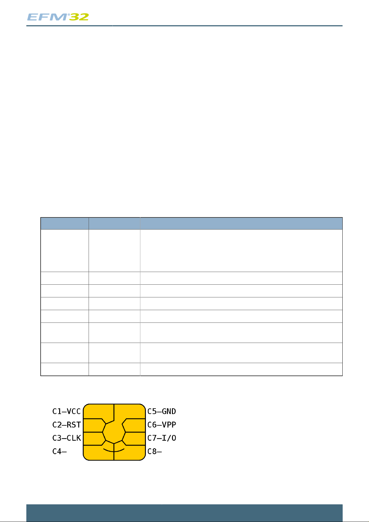
The following table contains the contact definition of the electrical contacts, according to ISO7816-2:
Table 2.1. Smart Card Electrical Connection
Contact Designation Use
C1 V
C2 RST Reset line (from reader to card)
C3 CLK Clock signal line (from reader to card)
C4 RFU Reserved for future use
C5 GND Common ground of contact reader and card
C6 V
C7 I/O Input/output data line that provides a half-duplex communication
C8 RFU Reserved for future use
cc
pp
Power connection through which operating power is supplied to the
microprocessor chip in the card (typically a reader must support up to
5V, max 200mA draw, but the device implemented in this example only
supports 3.3V since that is the operating voltage of the EFM32 on the
STK3700 starter kit.)
Higher voltage used to program EEPROM of older chips. Usually Not
used.
channel between the reader and the smart card
Figure 2.1. Smart Card Physical Connections
Figure 2.1 (p. 3) shows a typical pad layout of the contacts on the smart card.
2014-01-23 - an0820_Rev1.00 3
www.silabs.com
Page 4
...the world's most energy friendly microcontrollers
• 7816-3: Cards with contacts - Electrical interface and transmission protocols.
Describes the electrical levels and waveforms, as well as the physical layer of the communication
protocol. This part includes specification of clock generation, reset sequence, baud rate, frame and
parity check as well as negotiation of parameters related to the communication.
• 7816-4: Organization, security and commands for interchange.
It specifies the contents of command-response pairs exchanged at the interface, means of retrieval
of data elements and data objects in the card, applications and data in the card, access methods to
files and data in the card including a security architecture.
• 7816-5: Registration of application providers.
Defines how to use an application identifier to ascertain the presence of and/or perform the retrieval
of an application in a card. ISO/IEC 7816-5:2004 shows how to grant the uniqueness of application
identifiers.
The rest of the 7816 standard deals with security protocols, card management and life-cycle
management, cryptographic considerations and also newer types of smart card interfaces, including
synchronous communication and USB-enabled cards.
Since a USB CCID device operates as a bridge, relaying packets between host computer and smart
card, this application note will mainly relate to the electrical waveforms and transportation of messages
described in part 3 and 4 of the standard. These parts are discussed in detail in the following sections.
2.2 Part 3; Electrical Signal and Transmission Protocol
Communication with the smart card takes place over a single bi-directional, half-duplex data line. The
voltage levels for high / low states is the same as the supply voltage to the smart card. The direction
of communication is assumed to be known a-priori by both master (reader) and slave (smart card).
Parameters such as protocol format, type of smart card, baud rate and other electrical parameters are
read out of the smart card right after reset. This is known as the Answer to Reset or ATR. Based on the
information given in the ATR, the reader can adapt to the transmission format supported by the card.
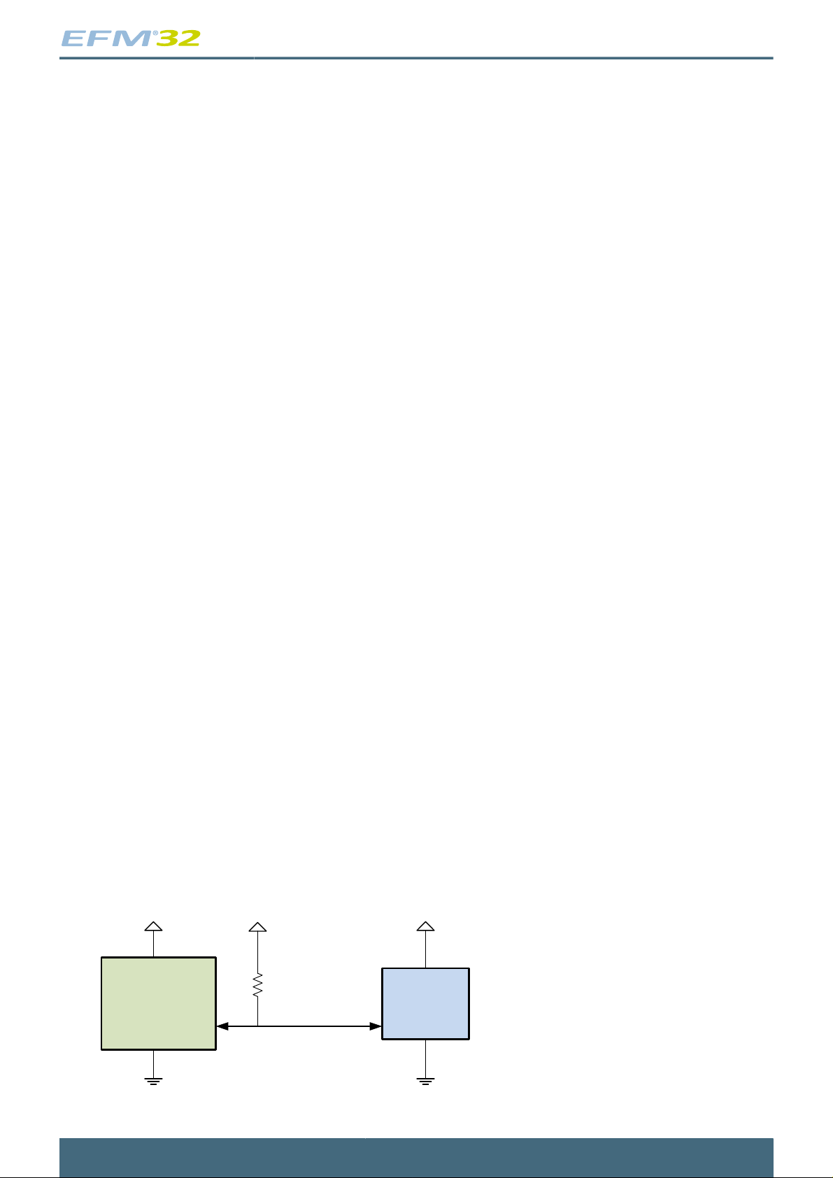
2.2.1 Electrical Connection of the Bi-directional Data Interface
Since the data communication is bi-directional, the terminal is often configured to transmit data through
an open-drain output. This means that it can pull the data line low, but it needs a pull-up resistor to go
high again. And in the same way, the smart card can pull the line low, but needs the pull-up to take the
line high again. Some interface-devices use more clever ways of doing this to achieve faster rise-times,
but for the EFM32 implementation of the bi-directional data line the following configuration is used:
Figure 2.2. Bi-directional Data Line with Pull-Up Resistor
Smart
R
pull
Smart
Card
Card
Terminal
2014-01-23 - an0820_Rev1.00 4
Data- line
www.silabs.com
Page 5
...the world's most energy friendly microcontrollers
The pull resistor used in the EFM32-implementation is the internal pull-up in the EFM32's GPIO pin.
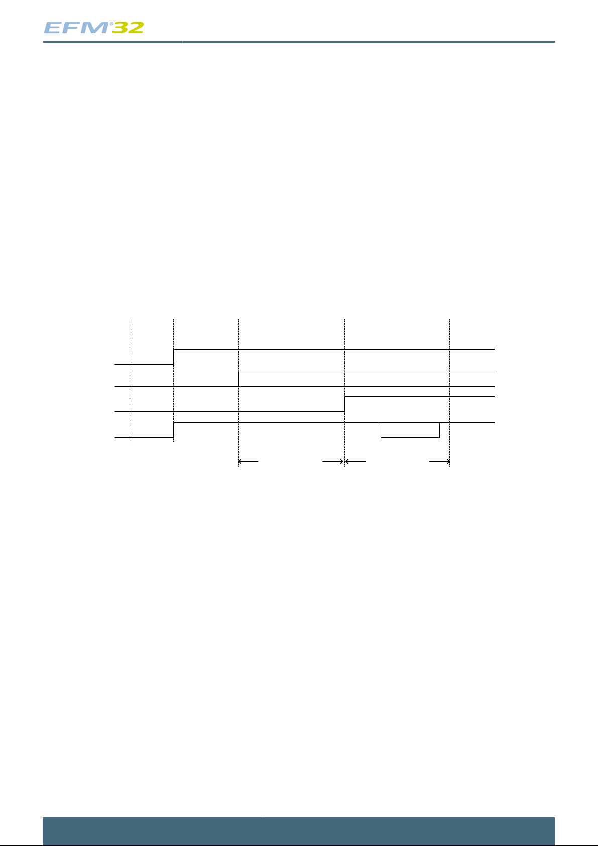
2.2.2 Power Up, Clock and Reset
When a card is inserted into the reader, all the contacts are disconnected from the terminal/reader,
including ground. The reason for this is that the contacts in the terminal slide over the smart card contacts
while the card is inserted. Applying power to the wrong pins could in theory damage the card or the
reader. When the card is properly inserted, there is usually an electrical contact that breaks connection,
indicating to the reader that the card is fully inserted. Now the reader initiates a power on and reset
sequence.
The interface is responsible for the timing of the sequence. The most important parameters are the clockcycle count before and after reset is released. The interface should enable the clock and keep it running
for 40k cycles before reset is released. After reset, the card must respond with its ATR within a window
of 400-40000 clock cycles. The timing is illustrated in Figure 2.3 (p. 5)
Figure 2.3. Answer to Reset Sequence
Vcc
Clk
Reset
IO
Card
Inserted
Power
enabled, IO-
pin pulled high
Clock
Started
Clock Running
Wait 40 000
clock cycles
Reset
Released
ATR
Received
ATR-Data
< 40 000
clock cycles
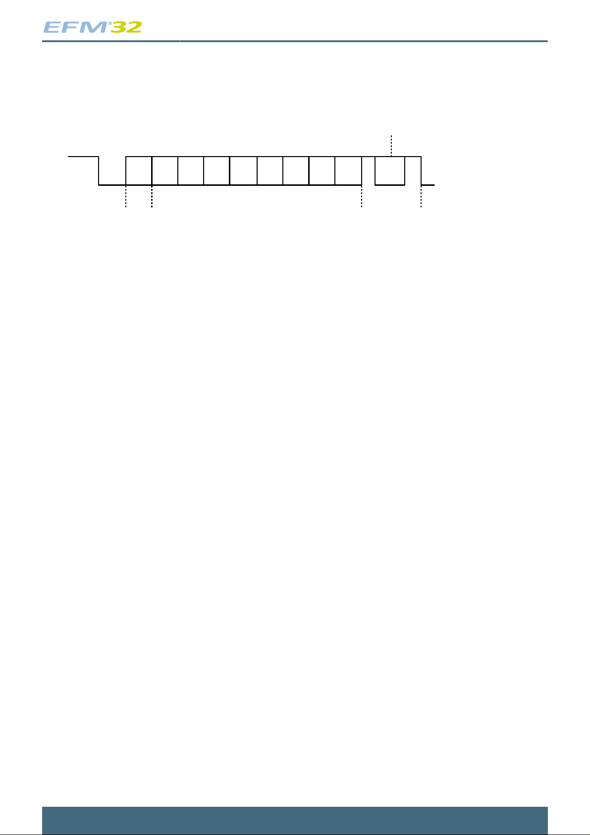
2.2.3 Byte Transfers
During the power on and reset sequence, the smart card answers with its "Answer to Reset". The
transmission of this first data-packet is carried out with default communication parameters listed below:
• Baud rate = F
• 8 data bits.
• 1 start bit.
• 1 parity bit, even.
• 1.5 stop bits (guard period for Ack/Nack).
• Coding of 0's and 1's: This can vary, the correct naming of this is: "Direct" or "Inverse" convention. It
is based on the very first character transmitted, called TS. "Direct" indicated by TS=HLHHLHHHLLH
(H = Vdd, L = GND) means that the following data is transferred as 0=GND, 1=Vdd and with the least
significant bit first. For the Inverse convention, indicated by TS=HLHHLLLLLLH, data is transmitted
with most significant bit first and 0=Vdd, 1=GND.
/372. Clock should be approximately 3.57 MHz, resulting in 9.6 kBaud/s.
clock
Using the above parameters, the interface must also adhere to the Ack/Nack of bytes, based on the
parity bit. A Nack is indicated when the receiver pulls the data line low in the guard period after the parity
bit is transmitted. If this happens, the transmitter should immediately retransmit the last byte.
One bit-period is called an "Elementary Time Unit" or ETU, this is used throughout the 7816 standard as a
basis for defining the timing of the protocol. An illustration of one transmitted byte is given in Figure 2.4 (p.
6) .
2014-01-23 - an0820_Rev1.00 5
www.silabs.com
Page 6
...the world's most energy friendly microcontrollers
Figure 2.4. Byte Transmission, Parity and Elementary Time Unit
Line pulled
low in case
of error
Start bit
8 bit Frame Parity bit
S 1 2 3 4 5 6 7 8 P Err
ETU
Guard Period
Elementary
Time Unit
Note that this byte-format with parity error detection is always used during the Answer to Reset, but only
for further communication if the selected protocol is "T=0" (based on what is indicated in the ATR). What
T=0 protocol means and why it is called that is explained in Section 2.3 (p. 6) .
2.2.4 Answer to Reset
The Answer to Reset is a string of 33 or fewer characters (bytes). With naming as defined in ISO 7816-3,
the ATR consists of the following mandatory and optional characters:
• TS - a mandatory initial character, conveying byte-format, (the direct or inverse convention).
• T0 - a mandatory format character, indicating the contents of the ATR.
• TAi, TBi, TCi, TDi - optional interface characters, these characters indicate supported clock speeds,
voltage levels and protocols supported by the card. Since they are optional, if not given, the card
reader must continue with the default protocol used during the ATR sequence.
• T1, T2, TK - optional historical characters, these characters typically hold information about the card
manufacturer, type of card (size etc.), version number and the state of the card.
• TCK - a conditional check character, presence of this byte is indicated by the optional interface
characters, if present, it is exclusive OR of all the bytes in the ATR, excluding TS and TCK.
This document will not go further into the meaning of these characters, please refer to the ISO 7816-3
Standard for more information, (Reference 1 (p. 20) ).
2.3 Part 4; Commands and Exchange of Data Packets
The previous section described how the first basic communication channel is established between the
card and the reader. The channel is a half-duplex, physical channel. Part 4 of the ISO 7816 standard
defines the link-level protocols on top of this physical channel. The link-level protocol provides an errorfree communication channel for the application-level protocol. This section describes the message
structure consisting of application protocol data units (APDUs), which are exchanged between the reader
application and the smart card application by the link-level protocol. Since only one type of the link-level
protocol is supported by the EFM32-reader-implementation (T=0), this will be described in more detail
than the others.
2014-01-23 - an0820_Rev1.00 6
www.silabs.com
Page 7
...the world's most energy friendly microcontrollers
Part 4 of the 7816 standard also defines a file system API to manipulate files and a security service API
allowing smart card and reader to mutually authenticate with each other. This is not discussed further
in this application note.
2.3.1 Protocol Data Units
The data units transmitted in the link-layer protocol is called transmission protocol data units (TPDUs).
These are the packets of data going between the reader and the smart card. On top of these are
the APDUs, which comes directly from the application layer of the protocol. The APDUs are usually
transmitted unaltered by the smart card interface device, but this depends on the level of automatism
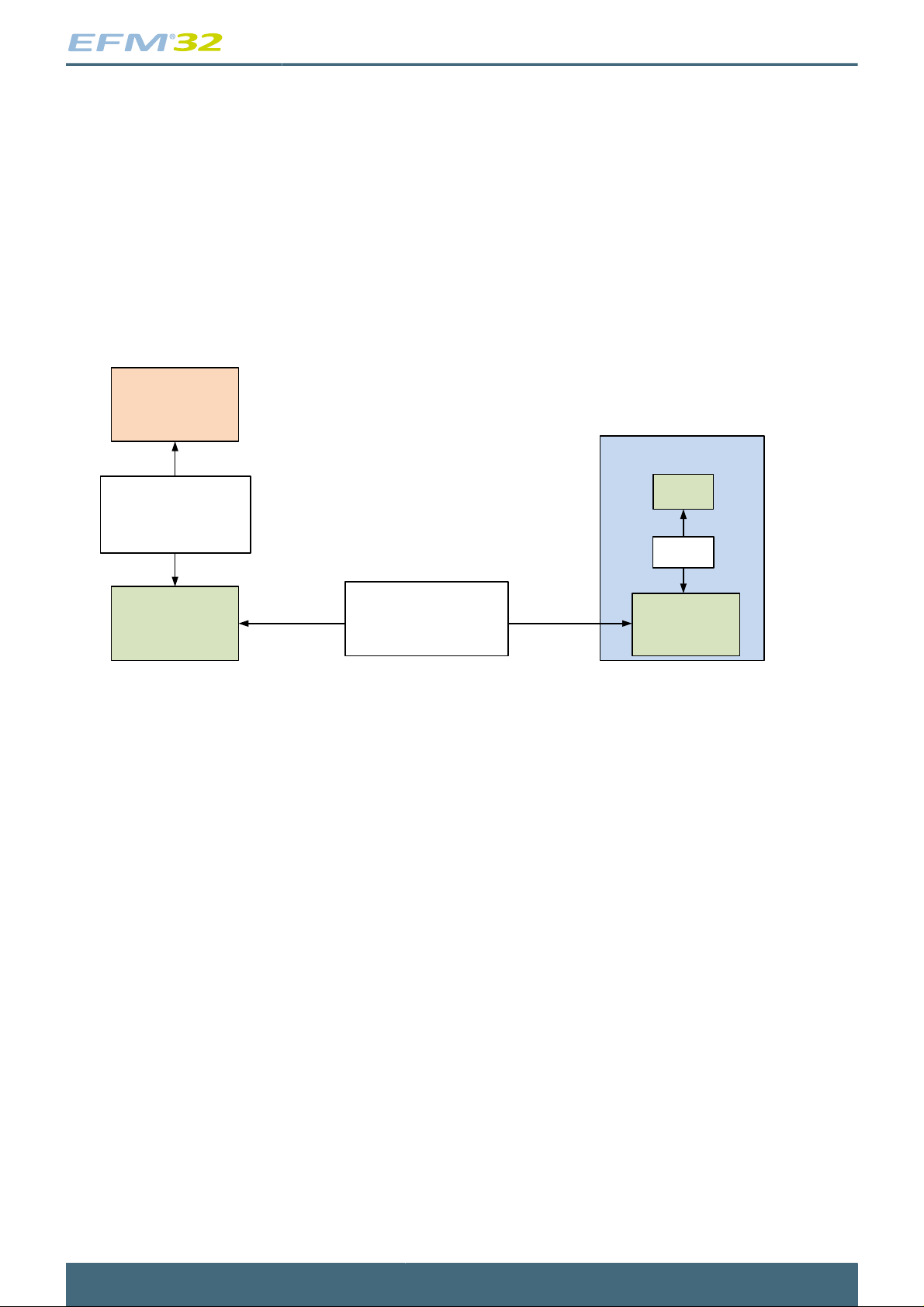
supported by the reader. This naming convention is illustrated in Figure 2.5 (p. 7) .
Figure 2.5. Protocol Data Units and Where they Apply
Host Application
Smart Card
Application Protocol
Data Units
(APDU)
Smart Card
Reader
Transmission Protocol
Data Units
(TPDU)
CPU
APDU
Physical/Link-
Layer
2.3.2 T=0 Protocol Introduction
The link-layer protocol is usually one of two variants, either a byte-oriented protocol with error handling
performed on each byte by using a parity bit, or a block-oriented protocol with checksum-based error
detection. The first one, the byte-oriented protocol is called "T=0". The name comes from the indication
of this protocol in the ATR by having one of the bits in one of the T-characters equal to 0. The blockoriented protocol is called "T=1". In fact there is even a T=2 protocol for full-duplex interfaces, with
T=3-15 reserved for future protocols.
The T=0 protocol re-uses the same byte-transmission format used during the ATR-sequence. The
parity error detection and retransmission at byte-level is also re-used. The TPDU-messages exchanged
between reader and smart card has two distinct structures, based on the direction of communication:
• A command, this is sent from reader to smart card. Consists of at least 5 characters named: CLA,
INS, P1, P2, P3, in addition comes a number of data bytes if writing to the smart card.
• CLA: Class designation of the command set to establish a collection of instructions.
• INS: The INS byte is used to identify a specific instruction within a class of instructions identified
by the CLA value.
• P1: Used to specify the addressing used by the [CLA, INS] instruction.
• P2: Also used to specify the addressing used by the [CLA, INS] instruction.
• P3: Specifies the number of data bytes transferred to or from the card as part of the [CLA, INS]
instruction execution.
• A response, this is sent from smart card to reader. Consists of 1 or 2 status characters named SW1
and SW2, in addition comes a number of data bytes if reading from the smart card. The SW1 byte
is also called "procedure-byte" if it is just an ACK or NULL character, indicating that the card is not
finished with the transaction.
2014-01-23 - an0820_Rev1.00 7
www.silabs.com
Page 8
...the world's most energy friendly microcontrollers
• SW1: Status response of the current command. 0x90 means success for example. If this byte is
equal to for instance 0x60=NULL or the INS sent in the command, it means the card need more
time to process the command or that it has more data to receive/send. This character is then called
a procedure byte.
• SW2: (optional) also conveys a status response to the reader
The flow of communication is handled by the reader depending on the first SW1 character of the smart
card-response. All transfers are initiated by the reader and followed by a response from the smart card.
In some cases, depending on SW1, the reader should wait for further bytes, in other cases it should
forward the SW1 and possibly SW2 characters and any read data bytes to the host application.
In the case of SW1 indicating that the reader should wait for further data or the smart card needs more
processing time, the SW1 is called a "procedure byte", indicating that it should not be forwarded to the
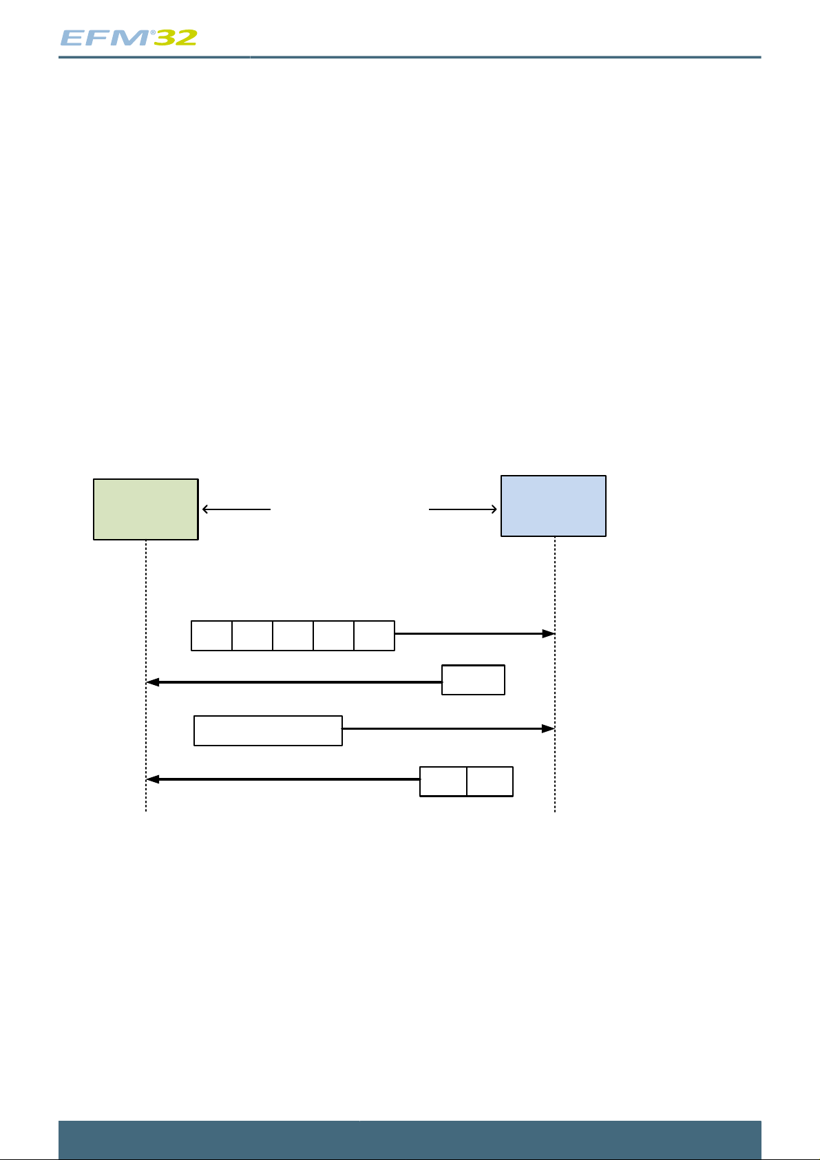
host application as a response. Figure 2.6 (p. 8) illustrates how transmission of a data packet to
the smart card looks like, following the T=0 protocol. In fact, for the T=0 protocol, the bytes of the APDU
directly overlays the bytes of the TPDU, this means that the APDU in Figure 2.6 (p. 8) simply
consists of CLA, INS, P1, P2, P3 and DATA in that order. Further, the APDU going back to the application
is simply SW1 and SW2.
Figure 2.6. Host Sends Data to Card
Smart Card
Terminal
7816- 3, T=0 Protocol
Smart Card
CLA INS P1 P2 P3
Procedure
byte
DATA
SW1 SW2
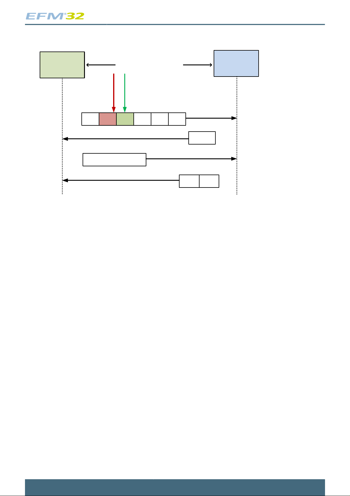
In the case of error on one byte using the T=0 protocol, the failing byte is retransmitted immediately by
the reader, this is illustrated in Figure 2.7 (p. 9) . Since the error detection is a single parity bit, this
will fail if there is an even number of bits flipped in the character transmitted. This is one of the limitations
of the T=0 protocol.
2014-01-23 - an0820_Rev1.00 8
www.silabs.com
Page 9
...the world's most energy friendly microcontrollers
Figure 2.7. Parity Error and Re-transmission for the T=0 Protocol
Smart Card
Terminal
7816- 3, T=0 Protocol
Parity
Error
CLA INS P1 P2 P3
Single Byte
Retransmitted
INS
Procedure
byte
Smart Card
DATA
SW1 SW2
For further explanation of CLA the (class byte), INS (instruction) and P1-3 (parameters) and their
contents in the T=0 protocol, please see the 7816 standard, (Reference 4 (p. 20) ).
2.3.3 T=1 Protocol Introduction
The T=1 protocol is more complex than the T=0 protocol. The physical interface is still half-duplex and
uses the same configuration as T=0. T=1 is actually built on top of T=0, but it does not use the T=0
error correction functionality, rather it uses a block oriented protocol. The main benefits of T=1 is the
block-oriented error detection mechanism which provides much better error detection and correction
capabilities than T=0. For more information about this protocol, please see Reference 2 (p. 20) .
2014-01-23 - an0820_Rev1.00 9
www.silabs.com
Page 10

...the world's most energy friendly microcontrollers
3 EFM32 USB CCID Implementation
The USB CCID (Circuit Card Interface Device) smart card reader in the attached software example,
implements a T=0 interface device only (byte-level transmission protocol, as defined in ISO/IEC 7816-3).
This means that the higher level details of the communication with the smart card (authentication, file
access etc.) is handled by the USB Host, which usually is a PC. Most of the protocol negotiation is also
handled by the host. The EFM32's job is to act as a USB - smart card bridge, transferring data packets
between the two and only handle T=0 protocol error conditions. For a complete implementation, other
error conditions such as electrical faults should also be detected and responded to accordingly, usually
by disconnecting the card immediately.
Figure 3.1 (p. 10) gives an overview of what is covered by the USB CCID standard (see Reference
1 (p. 20) ). It only covers the interface and protocol handling the transmission of APDU-packets
between the card reader and the USB host. The EFM32 implementation also includes the T=0 interface
protocol for communication with the smart card itself. From here on the EFM32 card reader is referred
to as the CCID.
Figure 3.1. Smart Card USB CCID Device Class Standard
USB CCID
Device Class
Standard
EFM32 Smart Card
Reader
3.1 USB CCID Standard
The CCID Standard (Reference 1 (p. 20) ) covers the USB communication including USB pipes used,
message formats, as well as all error conditions needed for conveying APDUs between the application
running on the USB host and the CCID. The format of the messages, message sizes and error-conditions
change according to the protocol used to communicate between the CCID and the smart card. This
makes it possible for the CCID to implement a high degree of automatism in the interaction with the
smart card. For instance, for T=1, which is block oriented, larger blocks of data can be transferred in
each USB packet to increase speed.
The CCID uses one Bulk-OUT Endpoint, one Bulk-In Endpoint and also one optional Interrupt Endpoint
to communicate with the host. Each message sent between Host and CCID contains a header which has
2014-01-23 - an0820_Rev1.00 10
www.silabs.com
Page 11

...the world's most energy friendly microcontrollers
a fixed length and a data field with variable length. Many of the messages consists only of the header.
Since the implementation in this application note only implements the T=0 protocol, the data field in the
USB messages typically map directly to the APDU-message going to/from the smart card.
A detailed description of the CCID standard is outside the scope of this document. For detailed
description of the CCID Class Descriptor, exact message format, status/error codes and sequence
diagrams, please refer to the specification, (Reference 1 (p. 20) ). An overview of some
implementation details, state-diagrams and sequence diagrams are given later in this chapter.
3.2 Connection of Smart Card to the STK
The EFM32 peripheral used for the physical layer is the USART which has a special 7816 smart card
mode to make the T=0 error detection and retransmission happen in hardware. An additional clock signal
is also required for the card, which is generated using a timer. As the serial communication is a single
line, half duplex, both the TX and the RX pins of the interface are tied together to the smart card I/O line,
this is done internally in the EFM32, using the loop back feature of the asynchronous serial interface.
According to ISO-7816 part 3, the nominal bit duration used on the I/O line is defined as one Elementary
Time Unit (ETU) and the initial ETU is 1/9600 s. For simplicity reasons, only the 9600 bps speed is
implemented. Further the bytes are transmitted using 8 data bits, 1 bit even parity and 1.5 stop bits, as
this matches the required format of the 7816 standard.
USART1 in asynchronous mode is used and TIMER0 provides the required clock signal. The clock
frequency is fixed to 3.5712 MHz which is the baud rate multiplied by 372. This is the default factor of
difference between baud rate and clock speed in the 7816 standard.
Further there is a reset pin and power pins allocated as well as a card-insertion detection pin. The 7816
standard defines that the card reader should physically power off the card if ordered to do so by the
host or if card-removal is detected.
The insertion detection pin is usually a separate electrical switch within the smart card socket. It is not
connected directly to the smart card. It is usually a normally closed switch, which opens when a smart
card is inserted all the way in the socket. In this example it is connected to both EFM32 GND and a
gpio-pin with a pull-up. When a card is inserted and the switch breaks the connection, it is expected that
this pin is pulled up. Therefore make sure to connect the other side of the insertion detection switch of
the card socket to EFM32-ground, not the GND pin of the smart card, as this can be tri-stated when
the card is not inserted.
All the pins used are located on the STK3700 expansion header, the exact pins used are described by
the following table:
Table 3.1. STK3700 Smart Card Pinout Description
EFM32GG990F1024 Smart Card Pin Functionality
PD2 C3 CLK Clock
PD0 C7 I/O line TX/RX Serial Data
PD5 C2 Reset Card reset
PD3 C1 V
PD4 C5 GND Ground pin of card
PD1 Insertion Detection Insertion Detect Pin, high
GND Insertion Detection Insertion Detect Pin, low
1
In this application example, a GPIO pin is used directly as the card power supply, hence the card Vcc is limited to 3.3V. For 5V
cards, the same application can be used with GPIO pin driving a hardware switch that provides Vcc=5V to the card.
2014-01-23 - an0820_Rev1.00 11
cc
Card Power Supply
side
side
www.silabs.com
1
Page 12

...the world's most energy friendly microcontrollers
The following picture illustrates how a physical smart card connector can be hooked up to the starter kit
on the above mentioned pins with some short wires.
Figure 3.2. Physical Connection of Card Socket with EFM32 Starterkit
3.3 Software Implementation
3.3.1 Supported Protocols and Cards
To make the software example as simple as possible, only a single communication protocol is supported,
the T=0 protocol. The CCID-standard also has optional lengths of APDU-packages, only the short type is
supported in this implementation. During development of the software, only cards from ACS, specifically
ACOS1 smart cards where used for testing. Other cards that support the same protocol should however
work, depending on host-side smart card driver and software.
Since the firmware on the EFM32 itself is basically only shuffling data-packets back and forth between
the smart card and the host computer, virtually any card supporting the correct speed and T=0 protocol
should be able to communicate with the host computer.
3.3.2 Software Algorithm
The software algorithm is based on a simple state machine function executed at regular intervals. About
every 10ms in this implementation, but anything down to 5-10 times per second should be OK. There are
no strict limitations on response time in the USB CCID-standard. The only time USB-interrupt messages
are sent, are upon card insertion or removal. All other communication happens through BulkIN/OUTendpoints.
Every time the CCID_Handler()-function is called, it steps the state-machine in Figure 3.3 (p. 13)
one step forward. All the actual CCID operations and communication with the smart card happens in the
"Handle USB-messages and CCID protocol"-transition.
2014-01-23 - an0820_Rev1.00 12
www.silabs.com
Page 13

...the world's most energy friendly microcontrollers
Figure 3.3. Card Detection and Notification Interrupt
Card Inserted
Usb- int: Notify
Slot Change
Wait for
Card
No Card
Card
Present
Card Removed
Usb- int: Notify
Slot Change
Handle USB-
messages and
CCID protocol
When one loop of the CCID_Handler is executed and the CCID either waits for a card or a card is present,
it reads one incoming USB-message and takes the necessary action. The three BulkOUT-messagetypes requiring any interaction with the card is the PC_to_Rdr_PowerOn/Off and PC_to_Rdr_XfrBlockmessages, see Reference 1 (p. 20) for more info.
The PowerOn message from the PC, requests the CCID to apply power to the smart card and it expects
the ATR in response.
The PowerOff message from the PC, requests the CCID to power off the smart card and expects only
a status message in return, indicating the new powered off state.
All actual communication with the card after the Answer to Reset, happens upon XfrBlock messages
from the PC. Each XfrBlock message contains one APDU which the CCID must send to the smart card
and in turn receive a response from the smart card which is sent back to the PC. Many APDUs only
expects the two status-bytes SW1 and SW2 as response. Some requests additional data and some has
data to write to the card. Figure 3.4 (p. 14) illustrates the communication procedure that the CCID
performs when it has an APDU that is to be sent to the smart card. Note that procedure byte 0x60 has
preference over 0x6X. "INS" refers to the instruction character in the APDU received from the host.
2014-01-23 - an0820_Rev1.00 13
www.silabs.com
Page 14

...the world's most energy friendly microcontrollers
Figure 3.4. Function Handling Command and Data Transfer with Smart Card
Send Command
Header
(CLA, INS, P1- P3)
Wait for Procedure
Byte from Card
Yes
No
If P- Byte =
NULL (0x60)
No
If P- Byte = INS
Yes
Send/ Receive
Data to/ from Card
Wait for
SW1, SW2 and
Return
2014-01-23 - an0820_Rev1.00 14
www.silabs.com
Page 15

...the world's most energy friendly microcontrollers
3.4 Typical Transaction Sequences
To further understand the typical communication pattern between both the PC and the CCID and
between the CCID and the smart card, it helps to look at how the transaction sequences play out
over time. This section has a couple of example-sequences indicating the difference between the
APDU- and TPDU-exchanges. Notice that all of these sequences follows the T=0 protocol. Also note
that the transaction diagram on the USB-side is simplified to only show the APDU-content of the
PC_to_RDR_XfrBlock USB-BulkOut messages, in addition these USB-messages actually contains a
fixed-length header-field with message-type, sequence numbering, status-bytes and so forth.
3.4.1 Sending Data to Card
When the host has data it wants to write to the smart card, it sends an APDU with data appended after
the mandatory CLA,INS,P123-header. The CCID sends first only the header to the smart card, it then
waits for a procedure byte, indicating what further action the CCID should take. See state-diagram in
Figure 3.4 (p. 14) for how the send-APDU function is implemented in the EFM32-based CCID.
If the procedure byte indicates that the smart card is ready to receive data, the CCID proceeds with
sending the data to the smart card. It then waits for a further procedure byte. Note that in the case
of successful transaction, the procedure byte is in fact the SW1-character and therefore part of the
response expected from the host. The CCID fetches the SW2 character as well and sends both SW1
and SW2 back to the host. See Figure 3.5 (p. 15) for an example-transaction of this sequence.
Figure 3.5. Host Sends Data to Card
Host- PC
CLA INS P1 P2 P3
DATA
SW1 SW2
3.4.2 Receiving Data from Card
EFM32
CCID
Reader
7816- 3, T= 0 ProtocolUSB
CLA INS P1 P2 P3
DATA
Procedure
byte
SW1 SW2
Smart Card
When the host has data it wants to read from the smart card it sends an APDU containing just a header,
which the CCID forwards directly to the smart card. The CCID must interpret the content of the APDU
to know that it is supposed to read data from the smart card and how many bytes it is supposed to
read. The CCID then waits for a procedure byte, and if indicating a data transmission the smart card
proceeds to send data after that the procedure byte. At the end of the data, the two status bytes, SW1
and SW2 are appended.
The CCID-response to the host is the data it received and the SW1 and SW2 bytes appended to the
end of the data. Figure 3.6 (p. 16) illustrates this smart card read transaction.
2014-01-23 - an0820_Rev1.00 15
www.silabs.com
Page 16

...the world's most energy friendly microcontrollers
Figure 3.6. Host Requests and Receives Data from Card
Host- PC
CLA INS P1 P2 P3
EFM32
CCID
Reader
CLA INS P1 P2 P3
SW1 SW2DATA
7816- 3, T= 0 ProtocolUSB
Procedure
DATA
SW1 SW2
Smart Card
byte
3.4.3 Insertion and Removal of Card
Figure 3.7 (p. 17) Illustrates the transaction patterns in the previous section with the addition of
insertion and removal of the card. Notice that the CCID does not power up the card until it receives a
PowerOn messages from the host. The CCID can implement automatic power on at insertion of a card,
but must then also advertise this feature in the USB-descriptor.
When the card is removed, the CCID should power off the card to protect from damage. It advertises that
the card is removed, and typically receives a power off message from the host. The CCID then replies
with a slotStatus message indicating that the card is not in the slot and that the slot is powered off.
2014-01-23 - an0820_Rev1.00 16
www.silabs.com
Page 17

...the world's most energy friendly microcontrollers
Figure 3.7. Sequence with Card Insertion, Removal and Simple Command
Host- PC
Bulk- OUT
IccPowerOn
Bulk- OUT
XfrBlock- Card
Cmd (no data)
Bulk- OUT
IccPowerOff
Interrupt – IN
NotifySlotChange
Bulk- IN
DataBlock-
AnswerToReset
Bulk- IN
DataBlock- Cmd
Response (SW1, SW2)
Interrupt – IN
NotifySlotChange
EFM32
CCID
Reader
7816- 3, T= 0 ProtocolUSB
Card Insertion Detected
Power On,
Enable Clock,
Release Reset
CLA INS P1 P2 P3
Card Removal Detected
Assert Reset,
Disable Clock,
Power Off
Smart Card
Answer To Reset
SW1 SW2
Bulk- IN
SlotStatus-
Card Removed
3.4.4 Timeout and Error Conditions
It can happen that the smart card stops responding or is malfunctioning in another way. To handle
this, the CCID should implement timeouts and error counters that signals the host with the appropriate
messages in the event of a malfunction. The EFM32 CCID-implementation includes some simple error
counters and timeout counters for this purpose, but it does not implement all the error conditions indicated
in the USB-CCID standard. It is usually ok to escalate many of the specific errors to timeout error as this
will trigger a power off of the smart card, which is always safe to do upon error conditions.
3.5 Use the Smart Card Reader with a PC
In order to make useful communication between a PC and the smart card happening, the host-computer
need software that can interact with the card. Typically, a windows PC will recognize the card-reader
as a smart card interface device. To get further, special software adapted to each different smart card
is needed. For the ACOS1/3 type of cards, there exists simple example software to store and retrieve
data on the smart card. One such software, available for free at the time of writing, which works with this
implementation is the "SmartCache"-software, (see Reference 3 (p. 20) ). This enables initialization
of the card, simple authentication with the card and storing/retrieving of data on the smart card itself.
Below is a screenshot of the "smart cache" application in action. The output is the result of probing an
already initialized ACOS1 smart card and reading out the answer to reset (ATR), as well as initialization
date and card-ID and card owner. Notice the authentication happening after the ATR is read out, but
before card ID and owner is available. It is necessary to put in the pin/password that was configured
when the card was initialized to get past the authentication. The pin/password can be changed later.
2014-01-23 - an0820_Rev1.00 17
www.silabs.com
Page 18

...the world's most energy friendly microcontrollers
Figure 3.8. SmartCache Application, result of "Get Info"-command
From the command prompt in windows, one can also retrieve the "Answer to Reset" of the smart card
by typing "certutil -scinfo".
Figure 3.9. Windows Command Prompt with output from "certutil -scinfo"
The screenshot above demonstrates use of the windows certutil function to read the smart card answer
to reset. This will verify that the USBCCID-device registered correctly with the Windows USBCCIDdriver. The errors above is likely to pop up if the inserted card is not initialized and prepared for further
certificate handling in Windows.
3.6 Limitations
There are some limitations with this implementation of a smart card reader that is important to be aware
of. First, the software only handles error- and warning-messages from the card in a simple way. Most of
2014-01-23 - an0820_Rev1.00 18
www.silabs.com
Page 19

...the world's most energy friendly microcontrollers
the responsibility of detecting errors is left to the host-computer, based on the responses given by the
card. There are no automatic negotiation of parameters and only a minimum sub-set of communication
protocols are implemented.
3.6.1 Adding a Level Translator and Protection Circuit
When connecting the smart card directly to the EFM32, it will only support 3.3V cards, smart cards
requiring 5V will not work when connected directly. Some cards need Vpp (programming voltage pin)
to be set to a higher programming voltage when writing to the card. This functionality is not supported
by the software and the Vpp pin is in fact not connected at all in this implementation. Also, there are
no additional ESD-protection or signal-conditioning when directly connected to the EFM32, which might
make the implementation more prone to electrical faults. There exists conditioning-devices that can
be connected between the mcu and the smart card, which handles ESD, signal conditioning and the
different voltage levels in a proper manner, see Figure 3.10 (p. 19) .
For further protection of the interface device and also adding support for different voltage levels, a
level translator circuit can be added between the EFM32 and the smart card itself. A typical connection
diagram for such a circuit is exemplified below.
Figure 3.10. Typical Connection Diagram with Level Translator and Protection Circuit
1.8- 5V
Reset
Clock
Data
GND
Smart Card
EFM32
3.3V
Reset
Clock
Data
Shutdown
Level-
Shift and
ESD
protection
Some simple level translators and protection devices for smart card interfaces exists. Two examples
of such a circuits are the Maxim DS8313/DS8314 devices and the Micrel MIC4555. These are analog
interface circuits with higher ESD protection than a typical microcontroller and also level-translating up
to 5V.
2014-01-23 - an0820_Rev1.00 19
www.silabs.com
Page 20

...the world's most energy friendly microcontrollers
4 References
1. Universal Serial Bus Device Class: Smart Card CCID Specification for Integrated Circuit(s) Cards
Interface Devices, Rev 1.1, 2005.
http://www.usb.org/developers/devclass_docs/DWG_Smart-Card_CCID_Rev110.pdf
2. Online version of ISO 7816 Standard:
http://www.cardwerk.com/smartcards/smartcard_standard_ISO7816.aspx
3. "Smart Cache" Windows software tool for storing data on ACOS-1/3 smart cards:
http://www.smartcache.net/
4. The home of the ISO-7816 standard:
http://www.iso.org
5. ACOS3 Smart Cards:
http://www.acs.com.hk/en/products/19/acos3-microprocessor-card/
2014-01-23 - an0820_Rev1.00 20
www.silabs.com
Page 21

5 Revision History
5.1 Revision 1.00
2014-01-23
Initial revision.
...the world's most energy friendly microcontrollers
2014-01-23 - an0820_Rev1.00 21
www.silabs.com
Page 22

...the world's most energy friendly microcontrollers
A Disclaimer and Trademarks
A.1 Disclaimer
Silicon Laboratories intends to provide customers with the latest, accurate, and in-depth documentation
of all peripherals and modules available for system and software implementers using or intending to use
the Silicon Laboratories products. Characterization data, available modules and peripherals, memory
sizes and memory addresses refer to each specific device, and "Typical" parameters provided can and
do vary in different applications. Application examples described herein are for illustrative purposes
only. Silicon Laboratories reserves the right to make changes without further notice and limitation to
product information, specifications, and descriptions herein, and does not give warranties as to the
accuracy or completeness of the included information. Silicon Laboratories shall have no liability for
the consequences of use of the information supplied herein. This document does not imply or express
copyright licenses granted hereunder to design or fabricate any integrated circuits. The products must
not be used within any Life Support System without the specific written consent of Silicon Laboratories.
A "Life Support System" is any product or system intended to support or sustain life and/or health, which,
if it fails, can be reasonably expected to result in significant personal injury or death. Silicon Laboratories
products are generally not intended for military applications. Silicon Laboratories products shall under no
circumstances be used in weapons of mass destruction including (but not limited to) nuclear, biological
or chemical weapons, or missiles capable of delivering such weapons.
A.2 Trademark Information
Silicon Laboratories Inc., Silicon Laboratories, Silicon Labs, SiLabs and the Silicon Labs logo, CMEMS®,
EFM, EFM32, EFR, Energy Micro, Energy Micro logo and combinations thereof, "the world’s most
energy friendly microcontrollers", Ember®, EZLink®, EZMac®, EZRadio®, EZRadioPRO®, DSPLL®,
ISOmodem®, Precision32®, ProSLIC®, SiPHY®, USBXpress® and others are trademarks or registered
trademarks of Silicon Laboratories Inc. ARM, CORTEX, Cortex-M3 and THUMB are trademarks or
registered trademarks of ARM Holdings. Keil is a registered trademark of ARM Limited. All other products
or brand names mentioned herein are trademarks of their respective holders.
2014-01-23 - an0820_Rev1.00 22
www.silabs.com
Page 23

...the world's most energy friendly microcontrollers
B Contact Information
Silicon Laboratories Inc.
400 West Cesar Chavez
Austin, TX 78701
Please visit the Silicon Labs Technical Support web page:
http://www.silabs.com/support/pages/contacttechnicalsupport.aspx
and register to submit a technical support request.
2014-01-23 - an0820_Rev1.00 23
www.silabs.com
Page 24

...the world's most energy friendly microcontrollers
Table of Contents
1. Smart Card Introduction ............................................................................................................................. 2
2. The ISO 7816 Standard ............................................................................................................................. 3
2.1. Different Parts of the 7816-Standard .................................................................................................. 3
2.2. Part 3; Electrical Signal and Transmission Protocol ............................................................................... 4
2.3. Part 4; Commands and Exchange of Data Packets ............................................................................... 6
3. EFM32 USB CCID Implementation ............................................................................................................. 10
3.1. USB CCID Standard ...................................................................................................................... 10
3.2. Connection of Smart Card to the STK ............................................................................................... 11
3.3. Software Implementation ................................................................................................................ 12
3.4. Typical Transaction Sequences ....................................................................................................... 15
3.5. Use the Smart Card Reader with a PC ............................................................................................. 17
3.6. Limitations ................................................................................................................................... 18
4. References ............................................................................................................................................. 20
5. Revision History ...................................................................................................................................... 21
5.1. Revision 1.00 ............................................................................................................................... 21
A. Disclaimer and Trademarks ....................................................................................................................... 22
A.1. Disclaimer ................................................................................................................................... 22
A.2. Trademark Information ................................................................................................................... 22
B. Contact Information ................................................................................................................................. 23
B.1. ................................................................................................................................................. 23
2014-01-23 - an0820_Rev1.00 24
www.silabs.com
Page 25

...the world's most energy friendly microcontrollers
List of Figures
2.1. Smart Card Physical Connections .............................................................................................................. 3
2.2. Bi-directional Data Line with Pull-Up Resistor ............................................................................................... 4
2.3. Answer to Reset Sequence ...................................................................................................................... 5
2.4. Byte Transmission, Parity and Elementary Time Unit ..................................................................................... 6
2.5. Protocol Data Units and Where they Apply .................................................................................................. 7
2.6. Host Sends Data to Card ......................................................................................................................... 8
2.7. Parity Error and Re-transmission for the T=0 Protocol ................................................................................... 9
3.1. Smart Card USB CCID Device Class Standard ........................................................................................... 10
3.2. Physical Connection of Card Socket with EFM32 Starterkit ........................................................................... 12
3.3. Card Detection and Notification Interrupt ................................................................................................... 13
3.4. Function Handling Command and Data Transfer with Smart Card ................................................................... 14
3.5. Host Sends Data to Card ....................................................................................................................... 15
3.6. Host Requests and Receives Data from Card ............................................................................................. 16
3.7. Sequence with Card Insertion, Removal and Simple Command ...................................................................... 17
3.8. SmartCache Application, result of "Get Info"-command ................................................................................. 18
3.9. Windows Command Prompt with output from "certutil -scinfo" ........................................................................ 18
3.10. Typical Connection Diagram with Level Translator and Protection Circuit ........................................................ 19
2014-01-23 - an0820_Rev1.00 25
www.silabs.com
Page 26

...the world's most energy friendly microcontrollers
List of Tables
2.1. Smart Card Electrical Connection .............................................................................................................. 3
3.1. STK3700 Smart Card Pinout Description ................................................................................................... 11
2014-01-23 - an0820_Rev1.00 26
www.silabs.com
Page 27

 Loading...