

Page 1
SINGLE-CHIP ETHERNET CONTROLLER
CP2200/1
Ethernet Controller
Integrated IEEE 802.3 MAC and 10 BASE-T PHY
Fully compatible with 100/1000 BASE-T networks
Full/Half duplex with auto-negotiation
Automatic polarity detection and correction
Automatic retransmission on collision
Automatic padding and CRC generation
Supports broadcast and multi-cast MAC addressing
Parallel Host Interface (30 Mbps Transfer Rate)
8-bit multiplexed or non-multiplexed mode
Only 11 I/O pins required in multiplexed mode
®
Intel
Interrupt on received packets and Wake-on-LAN
or Motorola® Bus Format
8 kB Flash Memory
8192 bytes ISP non-volatile memory
Factory pre-programmed unique 48-bit MAC Address
No external EEPROM required
Other Features
LED output drivers (Link/Activity)
Dedicated 2 kB RAM transmit buffer and 4 kB RAM
receive FIFO buffer
Power-on Reset
5 V Tolerant I/O
Software Support
Royalty-free TCP/IP stack with device drivers
TCP/IP Stack Configuration Wizard
Hardware diagnostic software and example code
Example Applications
Remote sensing and monitoring
Inventory management
VoIP phone adapters
Point-of-sale devices
Network clocks
Embedded Web Server
Remote Ethernet-to-UART bridge
Supply Voltage
3.1 to 3.6 V
Package
Pb-free 48-pin TQFP (9x9 mm footprint)
Pb-free 28-pin QFN (5x5 mm footprint)
Ordering Part Number
CP2200-GQ (48-pin)
CP2201-GM (28-pin)
Temperature Range: –40 to +85 °C
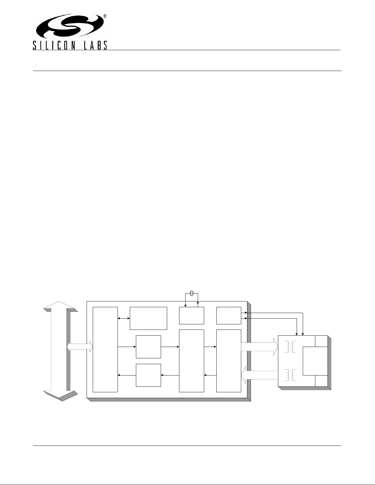
20 MHz
XTAL
CP2200
8 kB
Clock
Flash
Host
Interface
Parallel Bus
2 kB
Tx Buffer
Ethernet
MAC
4 kB
Rx FIFO
LED
Control
Ethernet
PHY
TX+/TX-
RX+/RX-
RJ-45
ACT
LED
LINK
LED
Figure 1. Example System Diagram
Rev. 1.0 5/07 Copyright © 2007 by Silicon Laboratories CP2200/1
Page 2

CP2200/1
2 Rev. 1.0
Page 3

CP2200/1
TABLE OF CONTENTS
Section Page
1. System Overview . . . . . . . . . . . . . . . . . . . . . . . . . . . . . . . . . . . . . . . . . . . . . . . . . . . . . . . . .5
2. Typical Connection Diagram . . . . . . . . . . . . . . . . . . . . . . . . . . . . . . . . . . . . . . . . . . . . . . . .6
3. Absolute Maximum Ratings . . . . . . . . . . . . . . . . . . . . . . . . . . . . . . . . . . . . . . . . . . . . . . . .8
4. Electrical Characteristics . . . . . . . . . . . . . . . . . . . . . . . . . . . . . . . . . . . . . . . . . . . . . . . . . . 9
5. Pinout and Package Definitions . . . . . . . . . . . . . . . . . . . . . . . . . . . . . . . . . . . . . . . . . . . .10
6. Functional Description . . . . . . . . . . . . . . . . . . . . . . . . . . . . . . . . . . . . . . . . . . . . . . . . . . .18
6.1. Overview . . . . . . . . . . . . . . . . . . . . . . . . . . . . . . . . . . . . . . . . . . . . . . . . . . . . . . . . . .18
6.2. Reset Initialization . . . . . . . . . . . . . . . . . . . . . . . . . . . . . . . . . . . . . . . . . . . . . . . . . . .18
6.3. Interrupt Request Signal . . . . . . . . . . . . . . . . . . . . . . . . . . . . . . . . . . . . . . . . . . . . . .18
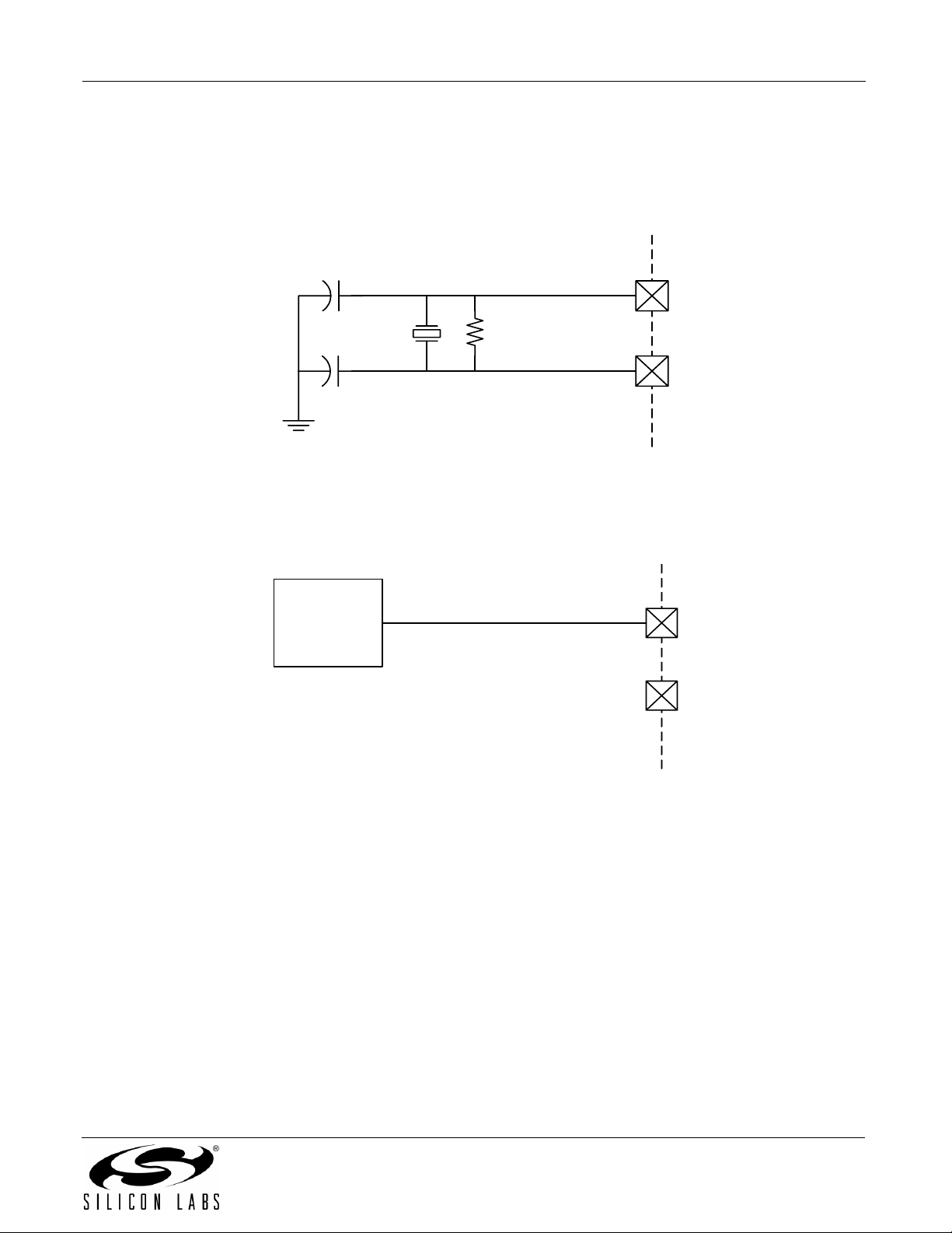
6.4. Clocking Options . . . . . . . . . . . . . . . . . . . . . . . . . . . . . . . . . . . . . . . . . . . . . . . . . . . .19
6.5. LED Control . . . . . . . . . . . . . . . . . . . . . . . . . . . . . . . . . . . . . . . . . . . . . . . . . . . . . . . .21
6.6. Sending and Receiving Packets . . . . . . . . . . . . . . . . . . . . . . . . . . . . . . . . . . . . . . . .22
7. Internal Memory and Registers . . . . . . . . . . . . . . . . . . . . . . . . . . . . . . . . . . . . . . . . . . . . .23
7.1. Random Access to RAM Transmit and Receive Buffers . . . . . . . . . . . . . . . . . . . . . . 23
7.2. Internal Registers . . . . . . . . . . . . . . . . . . . . . . . . . . . . . . . . . . . . . . . . . . . . . . . . . . .25
8. Interrupt Sources . . . . . . . . . . . . . . . . . . . . . . . . . . . . . . . . . . . . . . . . . . . . . . . . . . . . . . . . 30
9. Reset Sources . . . . . . . . . . . . . . . . . . . . . . . . . . . . . . . . . . . . . . . . . . . . . . . . . . . . . . . . . . 37
9.1. Power-On Reset . . . . . . . . . . . . . . . . . . . . . . . . . . . . . . . . . . . . . . . . . . . . . . . . . . . .38
9.2. Power-fail . . . . . . . . . . . . . . . . . . . . . . . . . . . . . . . . . . . . . . . . . . . . . . . . . . . . . . . . .39
9.3. Oscillator-Fail Reset . . . . . . . . . . . . . . . . . . . . . . . . . . . . . . . . . . . . . . . . . . . . . . . . . 39
9.4. External Pin Reset . . . . . . . . . . . . . . . . . . . . . . . . . . . . . . . . . . . . . . . . . . . . . . . . . .39
9.5. Software Reset . . . . . . . . . . . . . . . . . . . . . . . . . . . . . . . . . . . . . . . . . . . . . . . . . . . . . 40
9.6. Determining the Source of the Last Reset . . . . . . . . . . . . . . . . . . . . . . . . . . . . . . . . 41
9.7. De-Selecting Interrupt Sources . . . . . . . . . . . . . . . . . . . . . . . . . . . . . . . . . . . . . . . . .42
10. Power Modes . . . . . . . . . . . . . . . . . . . . . . . . . . . . . . . . . . . . . . . . . . . . . . . . . . . . . . . . . .43
10.1. Normal Mode . . . . . . . . . . . . . . . . . . . . . . . . . . . . . . . . . . . . . . . . . . . . . . . . . . . . . .44
10.2. Link Detection Mode . . . . . . . . . . . . . . . . . . . . . . . . . . . . . . . . . . . . . . . . . . . . . . . .44
10.3. Memory Mode . . . . . . . . . . . . . . . . . . . . . . . . . . . . . . . . . . . . . . . . . . . . . . . . . . . . . 44
10.4. Shutdown Mode . . . . . . . . . . . . . . . . . . . . . . . . . . . . . . . . . . . . . . . . . . . . . . . . . . . 44
10.5. Disabling Secondary Device Functions . . . . . . . . . . . . . . . . . . . . . . . . . . . . . . . . . . 45
11. Transmit Interface . . . . . . . . . . . . . . . . . . . . . . . . . . . . . . . . . . . . . . . . . . . . . . . . . . . . . .47
11.1. Overview . . . . . . . . . . . . . . . . . . . . . . . . . . . . . . . . . . . . . . . . . . . . . . . . . . . . . . . . .47
11.2. Transmitting a Packet . . . . . . . . . . . . . . . . . . . . . . . . . . . . . . . . . . . . . . . . . . . . . . .48
11.3. Overriding Transmit Configuration Options . . . . . . . . . . . . . . . . . . . . . . . . . . . . . . . 48
11.4. Transmit Buffer and AutoWrite Interface . . . . . . . . . . . . . . . . . . . . . . . . . . . . . . . . . 48
11.5. Transmit Status and Control Registers . . . . . . . . . . . . . . . . . . . . . . . . . . . . . . . . . .49
12. Receive Interface . . . . . . . . . . . . . . . . . . . . . . . . . . . . . . . . . . . . . . . . . . . . . . . . . . . . . . .58
12.1. Overview . . . . . . . . . . . . . . . . . . . . . . . . . . . . . . . . . . . . . . . . . . . . . . . . . . . . . . . . .58
12.2. Reading a Packet Using the Autoread Interface . . . . . . . . . . . . . . . . . . . . . . . . . . .58
12.3. Timing and Buffer Overflow Considerations . . . . . . . . . . . . . . . . . . . . . . . . . . . . . . 58
12.4. Initializing the Receive Buffer, Filter and Hash Table . . . . . . . . . . . . . . . . . . . . . . .59
Rev. 1.0 3
Page 4

CP2200/1
12.5. Receive Status and Control Registers . . . . . . . . . . . . . . . . . . . . . . . . . . . . . . . . . . 60
12.6. Advanced Receive Buffer Operation . . . . . . . . . . . . . . . . . . . . . . . . . . . . . . . . . . . . 66
12.7. Receive Buffer Advanced Status and Control Registers . . . . . . . . . . . . . . . . . . . . . 67
13. Flash Memory . . . . . . . . . . . . . . . . . . . . . . . . . . . . . . . . . . . . . . . . . . . . . . . . . . . . . . . . . .73
13.1. Programming the Flash Memory . . . . . . . . . . . . . . . . . . . . . . . . . . . . . . . . . . . . . . . 73
13.2. Reading the Flash Memory . . . . . . . . . . . . . . . . . . . . . . . . . . . . . . . . . . . . . . . . . . .74
13.3. Flash Access Registers . . . . . . . . . . . . . . . . . . . . . . . . . . . . . . . . . . . . . . . . . . . . . . 75
14. Media Access Controller (MAC) . . . . . . . . . . . . . . . . . . . . . . . . . . . . . . . . . . . . . . . . . . .78
14.1. Initializing the MAC . . . . . . . . . . . . . . . . . . . . . . . . . . . . . . . . . . . . . . . . . . . . . . . . .78
14.2. Accessing the Indirect MAC Registers . . . . . . . . . . . . . . . . . . . . . . . . . . . . . . . . . . 78
14.3. Indirect MAC Register Descriptions . . . . . . . . . . . . . . . . . . . . . . . . . . . . . . . . . . . .80
15. Physical Layer (PHY) . . . . . . . . . . . . . . . . . . . . . . . . . . . . . . . . . . . . . . . . . . . . . . . . . . . .88
15.1. Auto-Negotiation and Duplex Mode . . . . . . . . . . . . . . . . . . . . . . . . . . . . . . . . . . . . 88
15.2. Auto-Negotiation Synchronization . . . . . . . . . . . . . . . . . . . . . . . . . . . . . . . . . . . . . . 88
15.3. Loopback Mode . . . . . . . . . . . . . . . . . . . . . . . . . . . . . . . . . . . . . . . . . . . . . . . . . . . .89
15.4. Link Integrity Function . . . . . . . . . . . . . . . . . . . . . . . . . . . . . . . . . . . . . . . . . . . . . . .89
15.5. Receiver Smart Squelch and Automatic Polarity Correction . . . . . . . . . . . . . . . . . . 89
15.6. Transmitter Jabber Function . . . . . . . . . . . . . . . . . . . . . . . . . . . . . . . . . . . . . . . . . .89
15.7. Initializing the Physical Layer . . . . . . . . . . . . . . . . . . . . . . . . . . . . . . . . . . . . . . . . .90
16. Parallel Interface . . . . . . . . . . . . . . . . . . . . . . . . . . . . . . . . . . . . . . . . . . . . . . . . . . . . . . . .96
16.1. Non-Multiplexed Intel Format . . . . . . . . . . . . . . . . . . . . . . . . . . . . . . . . . . . . . . . . .96
16.2. Multiplexed Intel Format . . . . . . . . . . . . . . . . . . . . . . . . . . . . . . . . . . . . . . . . . . . . .98
16.3. Non-Multiplexed Motorola Format . . . . . . . . . . . . . . . . . . . . . . . . . . . . . . . . . . . . . 100
16.4. Multiplexed Motorola Format . . . . . . . . . . . . . . . . . . . . . . . . . . . . . . . . . . . . . . . . .102
Document Change List . . . . . . . . . . . . . . . . . . . . . . . . . . . . . . . . . . . . . . . . . . . . . . . . . . . .106
Contact Information . . . . . . . . . . . . . . . . . . . . . . . . . . . . . . . . . . . . . . . . . . . . . . . . . . . . . . .108
4 Rev. 1.0
Page 5

CP2200/1
1. System Overview
The CP2200/1 is a single-chip Ethernet controller containing an integrated IEEE 802.3 Ethernet Media Access
Controller (MAC), 10BASE-T Physical Layer (PHY), and 8 kB Non-Volatile Flash Memory available in a compact
5 x 5 mm QFN-28 package (sometimes called “MLF” or “MLP”) and a 48-pin TQFP package. The CP2200/1 can
add Ethernet connectivity to any microcontroller or host processor with 11 or more Port I/O pins. The 8-bit parallel
interface bus supports both Intel and Motorola bus formats in multiplexed and non-multiplexed mode. The data
transfer rate in non-multiplexed mode can exceed 30 Mbps.
The on-chip Flash memory may be used to store user constants, web server content, or as general purpose nonvolatile memory. The Flash is factory preprogrammed with a unique 48-bit MAC address stored in the last six
memory locations. Having a unique MAC address stored in the CP2200/1 often removes the serialization step from
the product manufacturing process of most embedded systems.
The CP2200/1 has four power modes with varying levels of functionality that allow the host processor to manage
the overall system power consumption. The optional interrupt pin also allows the host to enter a “sleep” mode and
awaken when a packet is received or when the CP2200/1 is plugged into a network. Auto-negotiation allows the
device to automatically detect the most efficient duplex mode (half/full duplex) supported by the network.
The Ethernet Development Kit (Ethernet-DK) bundles a C8051F120 MCU Target Board, CP2200 Ethernet
Development Board (AB4), the Silicon Laboratories IDE, all necessary debug hardware, and a TCP/IP
Configuration Wizard. The Ethernet Development Kit includes all hardware, software, and examples necessary to
design an embedded system using the CP2200. The CP2200 Ethernet Development Board is also compatible with
the C8051F020TB and C8051F340TB. Individual target boards may be purchased online by visiting
www.silabs.com.
Rev. 1.0 5
Page 6
CP2200/1
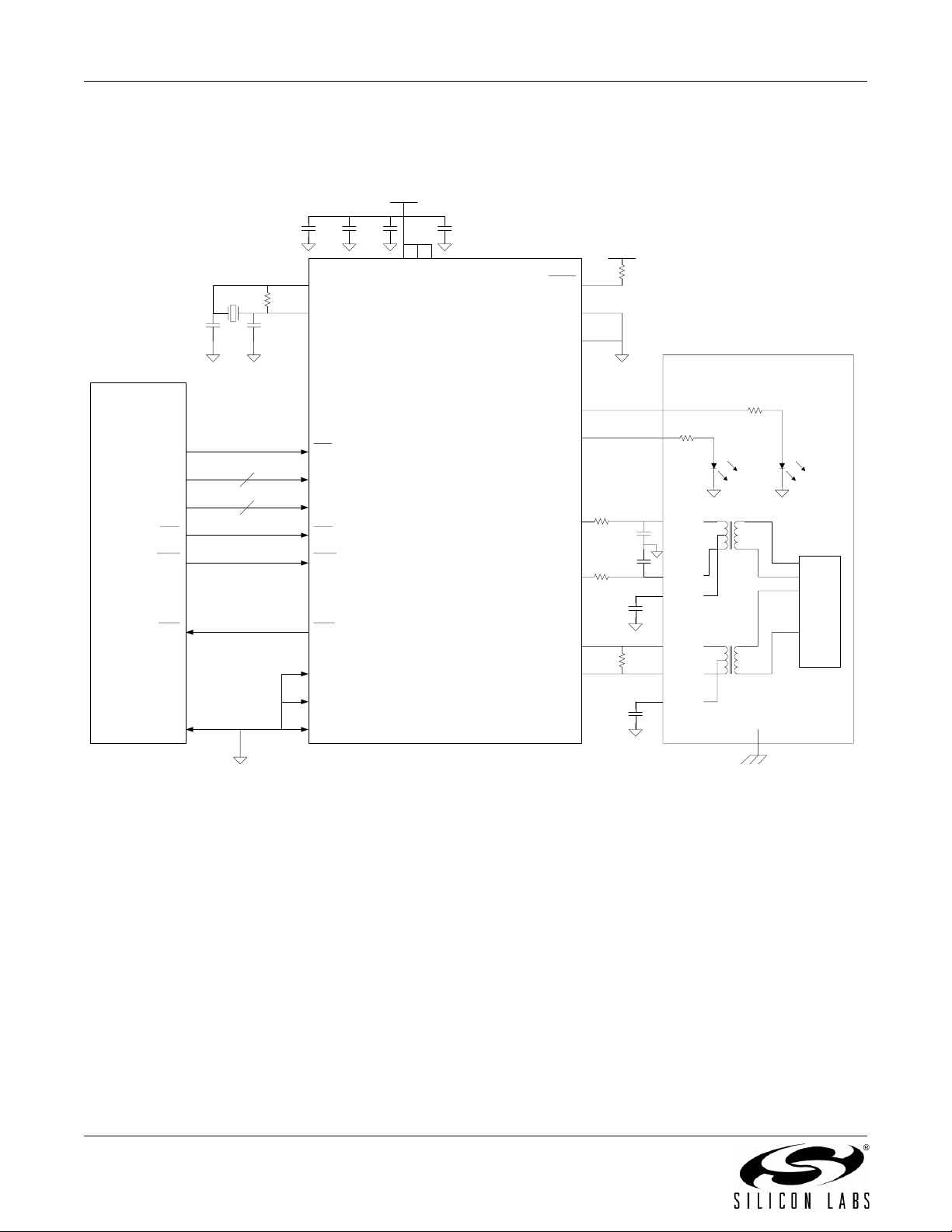
2. Typical Connection Diagram
Figure 2 and Figure 3 show typical connection diagrams for the 48-pin CP2200 and 28-pin CP2201.
+3VD
0.1 uF 0.1 uF 0.1 uF 10 uF
20 MHz
10 MΩ
22 pF22 pF
MCU
A15
A[7:0]
D[7:0] D[7:0]
RD RD
WR WR
Optional
8
8
Optional
XTAL1
XTAL2
CS
A[7:0]
INTINT
DGND1
AV+
VDD1
VDD2
CP2200
+3VD
4.7 kΩ
RST
MUXEN
MOTEN
Integrated RJ-45 Jack
LINK
ACT ACT LINK
TX+
TX–
RX+
RX–
8 Ω
0.001 uF
0.001 uF
8 Ω
0.1 uF
100 Ω
TXP
TXN
TCT
RXP
RXN
1:2.5
1:1
RJ-45
1
2
3
4
5
6
7
8
DGND2
GND AGND
0.1 uF
Note: The CP220x should be placed within 1 inch of the transformer for optimal performance.
Figure 2. Typical Connection Diagram (Non-Multiplexed)
RCT
Chassis
Ground
6 Rev. 1.0
Page 7
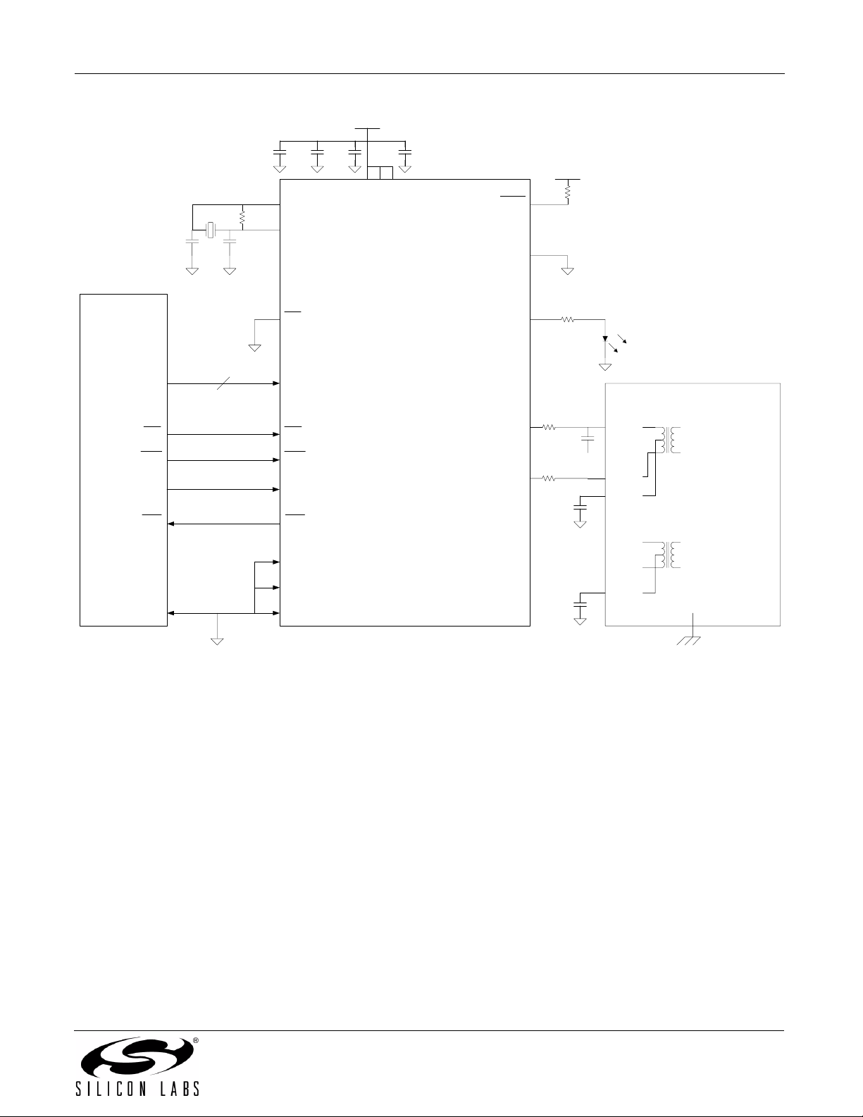
+3VD
CP2200/1
0.1 uF 0.1 uF 0.1 uF 10 uF
XTAL1
20 MHz
MCU
AD[7:0] AD[7:0]
10 MΩ
22 pF22 pF
XTAL2
CS
8
RD RD
WR WR
ALE ALE
Optional
INTINT
DGND1
DGND2
GND AGND
AV+
VDD1
VDD2
CP2201
+3VD
4.7 kΩ
RST
MOTEN
LA LINK/ACTIVITY
Integrated RJ-45 Jack
TX+
TX–
RX+
RX–
TXP
TXN
TCT
RXP
RXN
RCT
Figure 3. Typical Connection Diagram (Multiplexed)
Chassis
Ground
Rev. 1.0 7
Page 8

CP2200/1
3. Absolute Maximum Ratings
Table 1. Absolute Maximum Ratings
Parameter Conditions Min Typ Max Units
Ambient temperature under bias –55 — 125 °C
Storage Temperature –65 — 150 °C
Voltage on any I/O Pin or RST
Voltage on V
Maximum Total current through V
Maximum output current sunk by RST
Note: Stresses above those listed may cause permanent damage to the device. This is a stress rating only, and functional
operation of the devices at or exceeding the conditions in the operation listings of this specification is not implied.
Exposure to maximum rating conditions for extended periods may affect device reliability.
with respect to GND –0.3 — 4.2 V
DD
with respect to GND –0.3 — 5.8 V
and GND — — 500 mA
DD
or any I/O pin — — 100 mA
8 Rev. 1.0
Page 9

CP2200/1
4. Electrical Characteristics
Table 2. Global DC Electrical Characteristics
VDD= 3.1 to 3.6 V, –40 to +85 °C unless otherwise specified.
Parameter Conditions Min Typ Max Units
Supply Voltage 3.1 3.3 3.6 V
Supply Current in Normal Mode (Transmitting) V
Supply Current in Normal Mode (No Network
= 3.3 V — 75 155 mA
DD
V
=3.3 V — 60 — mA
DD
Traffic)
Supply Current with Transmitter and Receiver
V
=3.3 V — 47 — mA
DD
Disabled (Memory Mode)
Supply Current in Reset V
Supply Current in Shutdown Mode V
= 3.3 V — 15 — mA
DD
=3.3 V — 6.5 — mA
DD
Specified Operating Temperature Range –40 — +85 °C
Table 3. Digital I/O DC Electrical Characteristics
VDD= 3.1 to 3.6 V, –40 to +85 °C unless otherwise specified.
Parameters Conditions Min Typ Max UNITS
Output High Voltage (V
Output Low Voltage (V
Input High Voltage (V
Input Low Voltage (V
Input Leakage Current — 25 50 µA
)I
OH
)I
OL
)2.0——V
IH
)——0.8V
IL
OH
I
=–10µA
OH
I
=–10mA
OH
=8.5mA
OL
I
OL
I
OL
=–3mA
=10µA
=25mA
– 0.7
V
DD
V
– 0.1
DD
—
—
—
—
—
—
V
– 0.8
DD
—
—
1.0
—
—
—
0.6
0.1
—
V
V
Rev. 1.0 9
Page 10

CP2200/1
5. Pinout and Package Definitions
Table 4. CP2200/1 Pin Definitions
Name Pin Numbers Type Description
48-pin 28-pin
AV+ 5 3 Power In 3.1–3.6 V Analog Power Supply Voltage Input.
AGND 4 2 Analog Ground
V
DD1
DGND1 14 9 Digital Ground
V
DD2
DGND2 31 20 Digital Ground
RST
LINK 3* — D Out Link LED. Push-pull output driven high when valid 10BASE-T link
ACT 2* — D Out Activity LED. Push-pull output driven high for 50 ms when any
LA — 1* D Out Link or Activity LED. Push-pull output driven high when valid link
XTAL1 46 28 A In Crystal Input. This pin is the return for the external oscillator driver.
XTAL2 45* 27* A Out Crystal Output. This pin is the excitation driver for a quartz crystal.
13 8 Power In 3.1–3.6 V Digital Power Supply Voltage Input.
30 19 Power In 3.1–3.6 V Digital Power Supply Voltage Input.
15 10 D I/O Device Reset. Open-drain output of internal POR and VDD monitor.
An external source can initiate a system reset by driving this pin low
for at least 15 µs.
pulses are detected (Link Good) and driven low when valid
10BASE-T link pulses are not detected (Link Fail).
packet is transmitted or received and driven low all other times.
pulses are detected (Link Good) and driven low otherwise (Link
Fail). The output is toggled for each packet transmitted or received,
then returns to its original state after 50 ms.
This pin can be overdriven by an external CMOS clock.
TX+ 9 6 A Out 10BASE-T Transmit, Differential Output (Positive).
TX– 10 7 A Out 10BASE-T Transmit, Differential Output (Negative).
RX+ 7 5 A In 10BASE-T Receive, Differential Input (Positive).
RX– 6 4 A In 10BASE-T Receive, Differential Input (Negative).
MOTEN 43 26 D In Motorola Bus Format Enable. This pin should be tied directly to V
for Motorola bus format or directly to GND for Intel bus format.
MUXEN 44 — D In Multiplexed Bus Enable. This pin should be tied directly to V
multiplexed bus mode or directly to GND for non-multiplexed bus
mode.
INT
*Note: Pins can be left unconnected when not used.
10 Rev. 1.0
42 25 D Out Interrupt Service Request. This pin provides notification to the host.
DD
for
DD
Page 11

CP2200/1
Table 4. CP2200/1 Pin Definitions (Continued)
Name Pin Numbers Type Description
48-pin 28-pin
CS 41 24 D In Device Chip Select.
RD
/(DS) 39 22 D In Read Strobe (Intel Mode) or
Data Strobe (Motorola Mode)
WR
/(R/W) 40 23 D In Write Strobe (Intel Mode) or
Read/Write Strobe (Motorola Mode)
D0/AD0 16 11 D I/O Bit 0, Non-Multiplexed Data Bus or Multiplexed Address/Data Bus
D1/AD1 17 12 D I/O Bit 1, Non-Multiplexed Data Bus or Multiplexed Address/Data Bus
D2/AD2 18 13 D I/O Bit 2, Non-Multiplexed Data Bus or Multiplexed Address/Data Bus
D3/AD3 19 14 D I/O Bit 3, Non-Multiplexed Data Bus or Multiplexed Address/Data Bus
D4/AD4 20 15 D I/O Bit 4, Non-Multiplexed Data Bus or Multiplexed Address/Data Bus
D5/AD5 21 16 D I/O Bit 5, Non-Multiplexed Data Bus or Multiplexed Address/Data Bus
D6/AD6 22 17 D I/O Bit 6, Non-Multiplexed Data Bus or Multiplexed Address/Data Bus
D7/AD7 23 18 D I/O Bit 7, Non-Multiplexed Data Bus or Multiplexed Address/Data Bus
A0 27* — D In Bit 0, Non-Multiplexed Address Bus
A1 28* — D In Bit 1, Non-Multiplexed Address Bus
A2 29* — D In Bit 2, Non-Multiplexed Address Bus
A3/ALE/(AS) 32 — D In Bit 3, Non-Multiplexed Address Bus
ALE Strobe (Multiplexed Intel Mode)
Address Strobe (Multiplexed Motorola Mode)
ALE/(AS) — 21 D In ALE Strobe (Intel Mode)
Address Strobe (Motorola Mode)
A4 33* — D In Bit 4, Parallel Interface Non-Multiplexed Address Bus
A5 34* — D In Bit 5, Parallel Interface Non-Multiplexed Address Bus
A6 37* — D In Bit 6, Parallel Interface Non-Multiplexed Address Bus
A7 38* — D In Bit 7, Parallel Interface Non-Multiplexed Address Bus
NC 1, 8,
11,12
24–26
35,36
47, 48
— These pins should be left unconnected or tied to V
DD
.
*Note: Pins can be left unconnected when not used.
Rev. 1.0 11
Page 12
CP2200/1
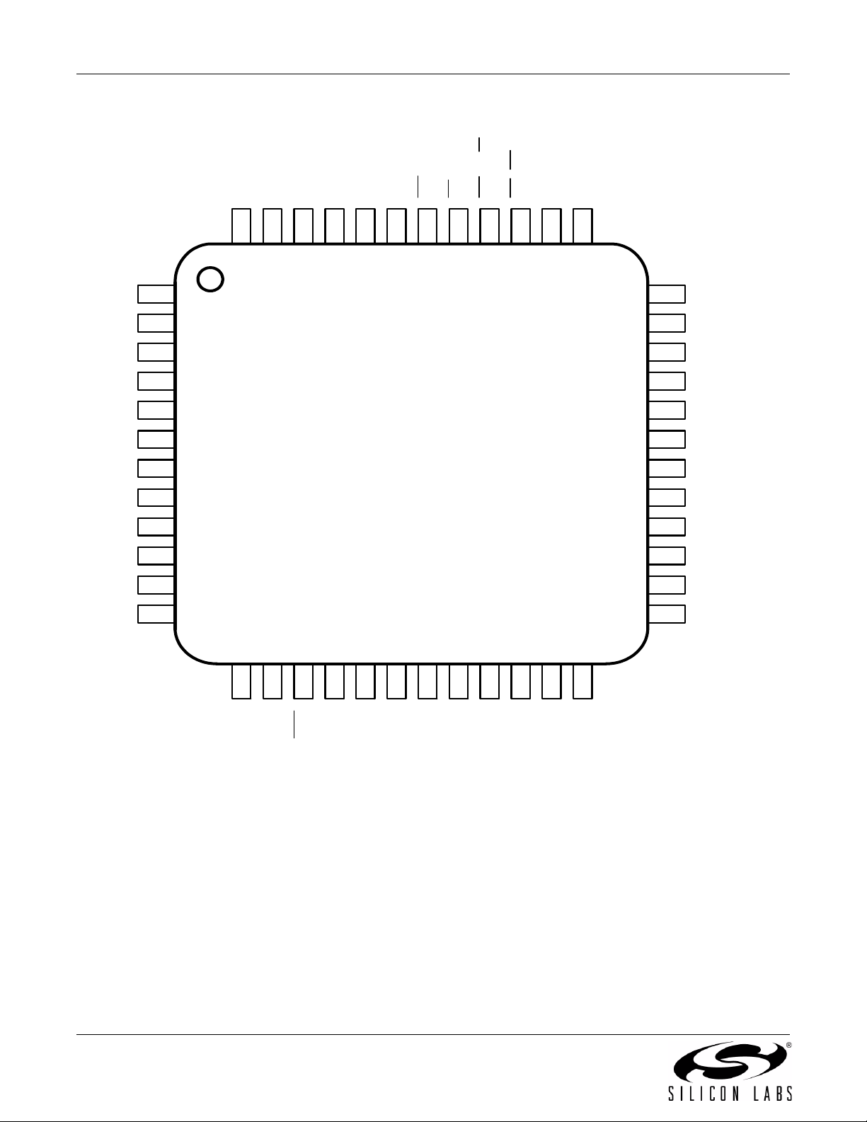
NC
48
NC
47
46
XTAL2
45
MUXEN
44
XTAL1
INT
MOTEN
43
42
CS
41
40
WR/(R/W)
39
38
A6
37
A7
RD/(DS)
NC
ACT
LINK
AGND
AV+
RX-
RX+
NC
TX+
TX-
NC
NC
10
11
12
1
2
3
4
5
6
7
8
9
13
14
15
CP2200
Top View
16
17
18
19
20
21
22
23
24
36
35
34
33
32
31
30
29
28
27
26
25
NC
NC
A5
A4
A3/ALE/(AS)
DGND2
VDD2
A2
A1
A0
NC
NC
VDD1
RST
DGND1
D1/AD1
D0/AD0
D2/AD2
D3/AD3
Figure 4. 48-pin TQFP Pinout Diagram
12 Rev. 1.0
D4/AD4
NC
D5/AD5
D6/AD6
D7/AD7
Page 13
48
PIN 1
IDENTIFIER
CP2200/1
D
D1
E1
E
1
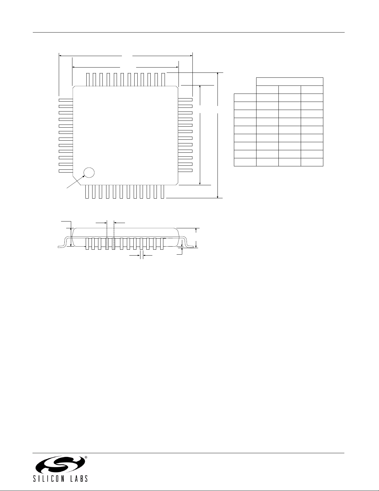
Table 5. TQFP-48 Package
Dimensions
MM
Min Typ Max
A——1.20
A1 0.05 — 0.15
A2 0.95 1.00 1.05
b 0.17 0.22 0.27
D — 9.00 —
D1 — 7.00 —
E — 9.00 —
e — 0.50 —
E1 — 7.00 —
A2
e
A
A1
b
Figure 5. 48-pin TQFP Package Dimensions
Rev. 1.0 13
Page 14

CP2200/1
Figure 6. QFN-28 Pinout Diagram (Top View)
14 Rev. 1.0
Page 15
CP2200/1
Bottom View
8
9
10
L
7
6
b
5
4
e
3
2
1
DETAIL 1
28
D2
27
D2
2
26
6 x e
12
13
E2
23
14
R
22
15
16
17
18
19
20
21
6 x e
11
2
E2
24
25
D
Side View
A2
A
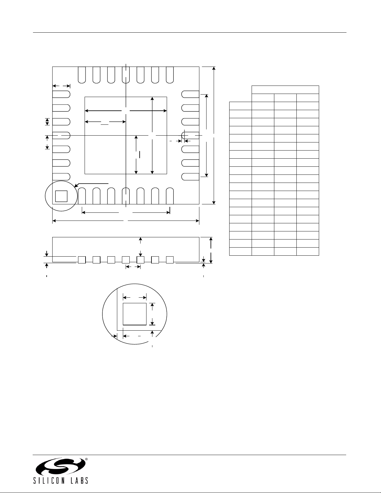
Table 6. QFN-28 Package
Dimensions
Min Typ Max
A 0.80 0.90 1.00
A1 0 0.02 0.05
A2 0 0.65 1.00
E
A3 — 0.25 —
b 0.18 0.23 0.30
D—5.00—
D2 2.90 3.15 3.35
E—5.00—
E2 2.90 3.15 3.35
e—0.5—
L 0.45 0.55 0.65
N—28—
ND — 7 —
NE — 7 —
R0.09— —
AA — 0.435 —
BB — 0.435 —
CC — 0.18 —
DD — 0.18 —
MM
A3
e
A1
DETAIL 1
AA
BB
CC
DD
Figure 7. QFN-28 Package Drawing
Rev. 1.0 15
Page 16
CP2200/1
Top View
0.85 mm
0.50 mm
0.20 mm
0.30 mm
0.20 mm
Connection
0.85 mm
0.50 mm
0.20 mm
Optional
GND
0.20 mm
0.30 mm
0.50 mm
0.10 mm
0.35 mm
b
D2
L
E2
e
0.50 mm
0.35 mm
0.10 mm
D
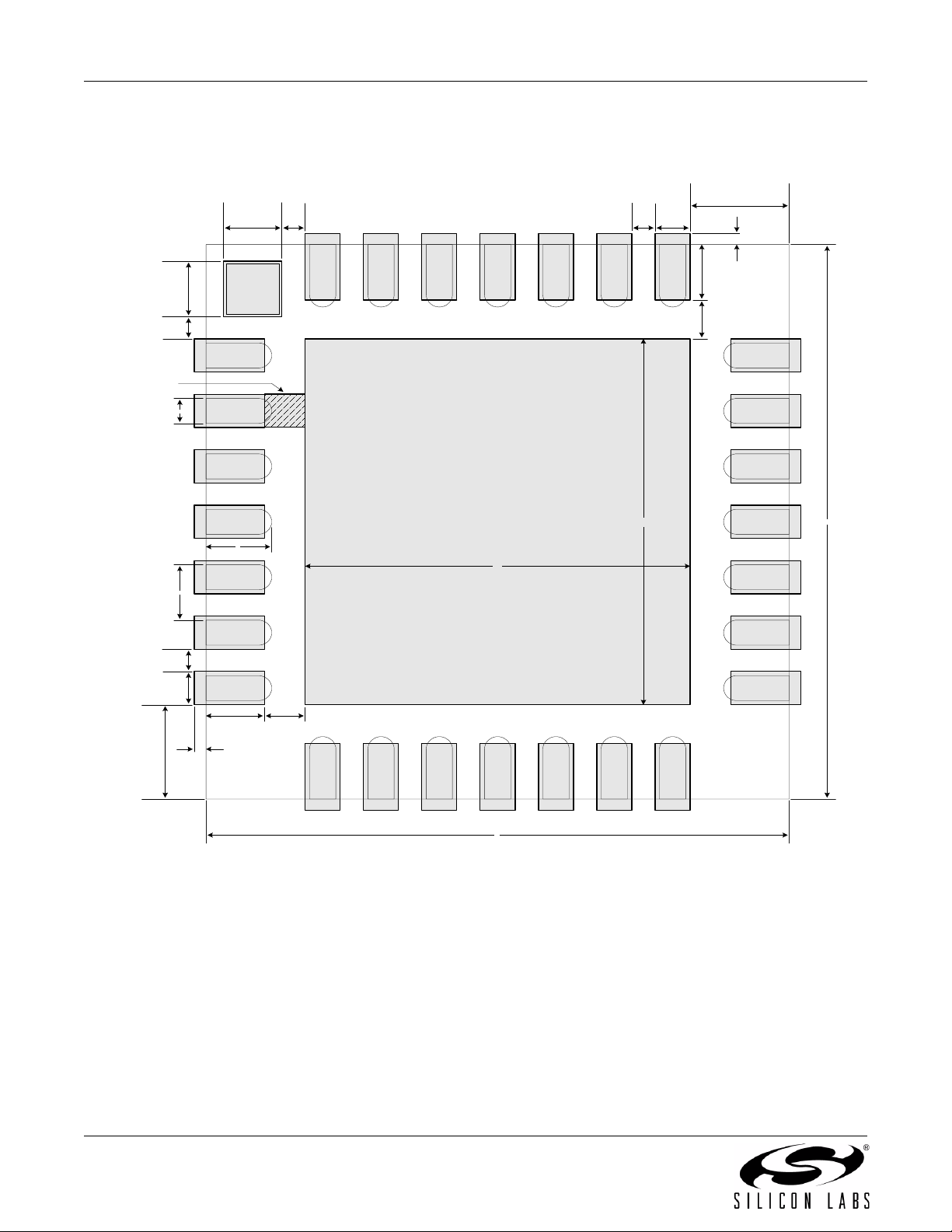
Figure 8. Typical QFN-28 Landing Diagram
16 Rev. 1.0
E
Page 17
0.50 mm
0.20 mm
Top View
0.20 mm
CP2200/1
0.85 mm
0.30 mm
0.85 mm
0.50 mm
0.20 mm
0.20 mm
0.30 mm
0.50 mm
0.10 mm
0.60 mm
0.60 mm
0.70 mm
b
L
e
E2
0.50 mm
0.35 mm
0.10 mm
0.30 mm
0.20 mm
0.40 mm
0.35 mm
D2
D
E
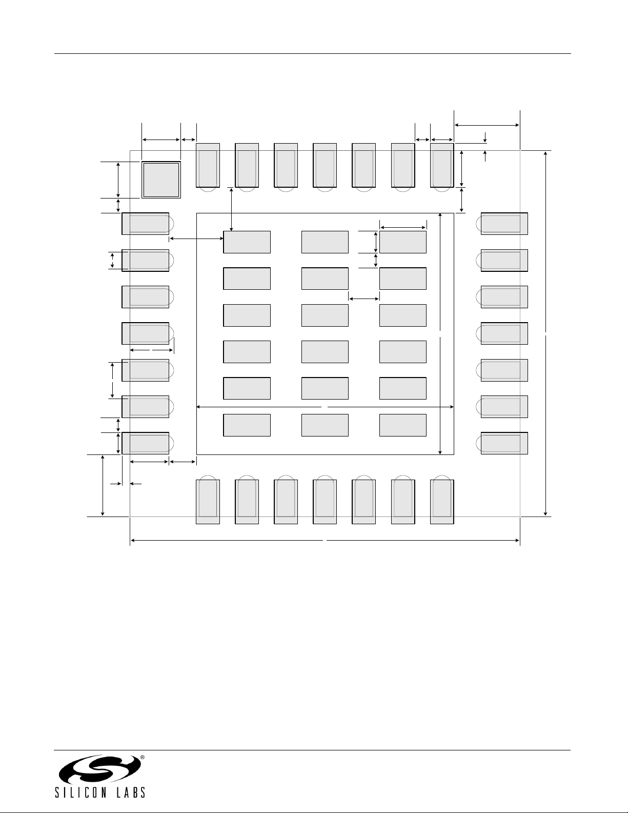
Figure 9. Typical QFN-28 Solder Paste Diagram
Rev. 1.0 17
Page 18

CP2200/1
6. Functional Description
6.1. Overview
In most systems, the CP2200/1 is used for transmitting and receiving Ethernet packets, non-volatile data storage,
and controlling Link and Activity LEDs. The device is controlled using direct and indirect internal registers
accessible through the parallel host interface. All digital pins on the device are 5 V tolerant.
6.2. Reset Initialization
After every CP2200/1 reset, the following initialization procedure is recommended to ensure proper device
operation:
Step 1: Wait for the reset pin to rise. This step takes the longest during a power-on reset.
Step 2: Wait for Oscillator Initialization to complete. The host processor will receive notification through the
interrupt request signal once the oscillator has stabilized.
Step 3: Wait for Self Initialization to complete. The INT0 interrupt status register on page 31 should be
checked to determine when Self Initialization completes.
Step 4: Disable interrupts (using INT0EN and INT1EN on page 33 and page 36) for events that will not be
monitored or handled by the host processor. By default, all interrupts are enabled after every reset.
Step 5: Initialize the physical layer. See “15.7. Initializing the Physical Layer” on page 90 for a detailed
physical layer initialization procedure.
Step 6: Enable the desired Activity, Link, or Activity/Link LEDs using the IOPWR register on page 45.
Step 7: Initialize the media access controller (MAC). See “14.1. Initializing the MAC” on page 78 for a
detailed MAC initialization procedure.
Step 8: Configure the receive filter. See “12.4. Initializing the Receive Buffer, Filter and Hash Table” on
page 59 for a detailed initialization procedure.
Step 9: The CP2200/1 is ready to transmit and receive packets.
6.3. Interrupt Request Signal
The CP2200/1 has an interrupt request signal (INT) that can be used to notify the host processor of pending
interrupts. The INT
dedicate a port pin to the INT
generating events have occurred. If the /INT signal is not used, pending interrupts such a Receive FIFO Full must
still be serviced.
The 14 interrupt sources are listed below. Interrupts are enabled on reset and can be disabled by software.
Pending interrupts can be cleared (allowing the INT
registers. See “8. Interrupt Sources” on page 30 for a complete description of the CP2200/1 interrupts.
End of Packet Reached Packet Received
Receive FIFO Empty “Wake-on-LAN” Wakeup Event
Receive FIFO Full Link Status Changed
Oscillator Initialization Complete Jabber Detected
Self Initialization Complete Auto-Negotiation Failed
Flash Write/Erase Complete Remote Fault Notification
Packet Transmitted Auto-Negotiation Complete
signal is asserted upon detection of any enabled interrupt event. Host processors that cannot
signal can periodically poll the interrupt status registers to see if any interrupt
signal to de-assert) by reading the self-clearing interrupt
18 Rev. 1.0
Page 19
CP2200/1
6.4. Clocking Options
The CP2200/1 can be clocked from an external parallel-mode crystal oscillator or CMOS clock. Figure 10 and
Figure 11 show typical connections for both clock source types. If a crystal oscillator is chosen to clock the device,
the crystal is started once the device is released from reset and remains on until the device reenters the reset state
or loses power.
XTAL1
10 MΩ20 MHz
XTAL2
Figure 10. Crystal Oscillator Example
Important note on external crystals: Crystal oscillator circuits are quite sensitive to PCB layout. The crystal
should be placed as close as possible to the XTAL pins on the device. The traces should be as short as possible
and shielded with a ground plane from any other traces that could introduce noise or interference.
20 MHz
XTAL1
CMOS
Clock
XTAL2
No Connect
Figure 11. External CMOS Clock Example
Table 7 lists the clocking requirements of the CP2200/1 when using a crystal oscillator or CMOS clock. Table 8
shows the electrical characteristics of the XTAL1 pin. These characteristics are useful when selecting an external
CMOS clock.
Rev. 1.0 19
Page 20

CP2200/1
Table 7. Clocking Requirements
VDD= 3.1 to 3.6 V, –40 to +85 °C unless otherwise specified.
Parameters Conditions Min Typ Max UNITS
Frequency — 20 — MHz
Frequency Error — —
Duty Cycle 455055%
Table 8. Input Clock Pin (XTAL1) DC Electrical Characteristics
VDD= 3.1 to 3.6 V, –40 to +85 °C unless otherwise specified.
Parameters Conditions Min Typ Max UNITS
XTAL1 Input Low Voltage — — 0.7 V
XTAL1 Input High Voltage 2.0 — — V
±50 ppm
20 Rev. 1.0
Page 21
CP2200/1
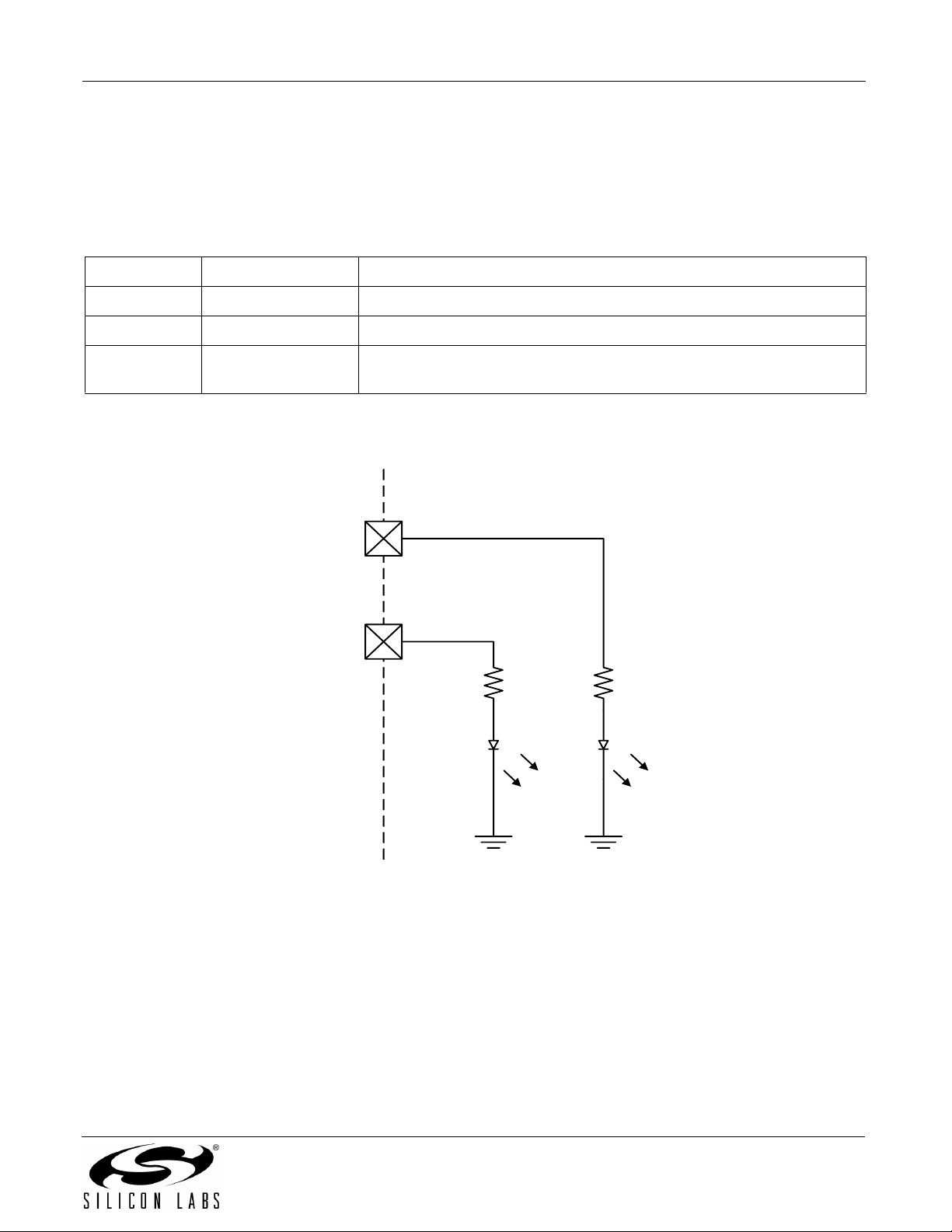
6.5. LED Control
The CP2200/1 can be used to control link status and activity LEDs. The CP2200 (48-pin TQFP) has two push-pull
LED drivers that can source up to 10 mA each. The CP2201 (28-pin QFN) has a single push-pull LED driver that
turns the LED on or off based on the link status and blinks the LED when activity is detected on a good link. Table 9
shows the function of the LED signals available on the CP2200/1.
Table 9 .
Signal Device Description
LINK CP2200 Asserted when valid link pulses are detected.
ACT CP2200 Asserted for 50 ms for each packet transmitted or received.
LA CP2201 Asserted when valid link pulses are detected and toggled for 50 ms for
each packet transmitted or received.
Figure 12 shows a typical LED connection for the CP2200. The CP2201 uses an identical connection for the LA
(link/activity) pin. The LED drivers are enabled and disabled using the IOPWR register on page 45.
LED Control Signals
LINK
ACT
Figure 12. LED Control Example (CP2200)
Rev. 1.0 21
Page 22

CP2200/1
6.6. Sending and Receiving Packets
After reset initialization is complete, the CP2200/1 is ready to send and receive packets. Packets are sent by
loading data into the transmit buffer using the AutoWrite register and writing ‘1’ to TXGO. See “11.2. Transmitting a
Packet” on page 48 for detailed information on how to transmit a packet using the transmit interface. A Packet
Transmitted interrupt will be generated once transmission is complete.
Packet reception occurs automatically when reception is enabled in the MAC and the receive buffer is not full.
Once a packet is received, the host processor is notified by generating a Packet Received interrupt. The host may
read the packet using the AutoRead interface. See “12.2. Reading a Packet Using the Autoread Interface” on
page 58 and “12.4. Initializing the Receive Buffer, Filter and Hash Table” on page 59 for additional information on
using and initializing the receive interface.
22 Rev. 1.0
Page 23
CP2200/1
7. Internal Memory and Registers
The CP2200/1 is controlled through direct and indirect registers accessible through the parallel host interface. The
host interface provides an 8-bit address space, of which there are 114 valid direct register locations (see Table 11
on page 25). All remaining addresses in the memory space are reserved and should not be read or written. The
direct registers provide access to the RAM buffers, Flash memory, indirect MAC configuration registers, and other
status and control registers for various device functions.
Figure 13 shows the RAM and Flash memory organization. The transmit and receive RAM buffers share the same
address space and are both accessed using the RAMADDRH:RAMADDRL pointer. Each of the buffers has a
dedicated data register. The Flash memory has a separate address space and a dedicated address pointer and
data register. See “13. Flash Memory” on page 73 for detailed information on how to read and write to Flash.
Transmit Buffer (2K)
0x0000 – 0x07FF
Receive Buffer (4K)
0x0000 – 0x0FFF
Flash Memory (8K)
0x0000 – 0x1FFF
RAMADDRH:RAMADDRL FLASHADDRH:FLASHADDRL
Figure 13. RAM Buffers and Flash Memory Organization
7.1. Random Access to RAM Transmit and Receive Buffers
The most common and most efficient methods for accessing the transmit and receive buffers are the AutoWrite
and AutoRead interfaces. These interfaces allow entire packets to be written or read at a time. In very few cases,
the transmit and receive buffers may need to be accessed randomly. An example of this is a system in which a
specific byte in the packet is checked to determine whether to read the packet or discard it. The following
procedure can be used to read or write data to either RAM buffer:
Step 1: Write the address of the target byte to RAMADDRH:RAMADDRL.
Step 2: Transmit Buffer:
Read or write 8-bit data to RAMTXDATA to read or write from the target byte in the transmit buffer.
Receive Buffer:
Read or write 8-bit data to RAMRXDATA to read or write from the target byte in the receive buffer.
Note: Reads and writes of the RAM buffers using the random access method are independent of the
AutoRead and AutoWrite interfaces. Each of the interfaces has a dedicated set of address and data
registers. See “11.2. Transmitting a Packet” on page 48 and “12.2. Reading a Packet Using the
Autoread Interface” on page 58 for additional information about the AutoRead and AutoWrite
interfaces.
Rev. 1.0 23
Page 24

CP2200/1
Register 1. RAMADDRH: RAM Address Pointer High Byte
R/W R/W R/W R/W R/W R/W R/W R/W Reset Value
Bit7 Bit6 Bit5 Bit4 Bit3 Bit2 Bit1 Bit0 Address:
Bits7–0: RAMADDRH: RAM Address Register High Byte
Holds the most significant eight bits of the target RAM address.
Register 2. RAMADDRL: RAM Address Pointer Low Byte
R/W R/W R/W R/W R/W R/W R/W R/W Reset Value
Bit7 Bit6 Bit5 Bit4 Bit3 Bit2 Bit1 Bit0 Address:
Bits7–0: RAMADDRL: RAM Address Register Low Byte
Holds the least significant eight bits of the target RAM address.
00000000
0x08
00000000
0x09
Register 3. RAMTXDATA: RAM Transmit Buffer Data Register
R/W R/W R/W R/W R/W R/W R/W R/W Reset Value
00000000
Bit7 Bit6 Bit5 Bit4 Bit3 Bit2 Bit1 Bit0 Address:
Bits7–0: RAMTXDATA: Transmit Buffer Data Register
Read: Returns data in the transmit buffer at location RAMADDRH:RAMADDRL.
Write: Writes data to the transmit buffer at location RAMADDRH:RAMADDRL.
Register 4. RAMRXDATA: RAM Receive Buffer Data Register
R/W R/W R/W R/W R/W R/W R/W R/W Reset Value
00000000
Bit7 Bit6 Bit5 Bit4 Bit3 Bit2 Bit1 Bit0 Address:
Bits7–0: RAMRXDATA: Receive Buffer Data Register
Read: Returns data in the receive buffer at location RAMADDRH:RAMADDRL.
Write: Writes data to the receive buffer at location RAMADDRH:RAMADDRL.
0x04
0x02
24 Rev. 1.0
Page 25

CP2200/1
7.2. Internal Registers
The CP2200/1 has 114 direct internal registers and 9 indirect registers. The registers are grouped into ten
categories based on function. Table 10 lists the register groups and provides links to the detailed register
descriptions for each group. Table 11 lists all direct registers available on the device.
Table 10. CP2200/1 Register Groups
RAM Access Registers Section 7.1 on page 23
Interrupt Status and Control Registers Section 8 on page 30
Reset Source Registers Section 9 on page 37
Power Mode Registers Section 10 on page 43
Transmit Status and Control Registers Section 11.5 on page 49
Receive Interface Status and Control Registers Section 12.5 on page 60
Receive Buffer Status and Control Registers Section 12.7 on page 67
FLASH Access Registers Section 13.3 on page 75
MAC Access Registers Section 14.2 on page 78
MAC Indirect Registers Section 14.3 on page 80
PHY Status and Control Registers Section 15 on page 88
Table 11. Direct Registers
Register Address Description Page No.
CPADDRH 0x21 Current RX Packet Address High Byte page 65
CPADDRL 0x22 Current RX Packet Address Low Byte page 65
CPINFOH 0x1D Current RX Packet Information High Byte page 63
CPINFOL 0x1E Current RX Packet Information Low Byte page 64
CPLENH 0x1F Current RX Packet Length High Byte page 64
CPLENL 0x20 Current RX Packet Length Low Byte page 64
CPTLB 0x1A Current RX Packet TLB Number page 67
FLASHADDRH 0x69 Flash Address Pointer High Byte page 76
FLASHADDRL 0x68 Flash Address Pointer Low Byte page 76
FLASHAUTORD 0x05 Flash AutoRead w/ increment page 77
FLASHDATA 0x06 Flash Read/Write Data Register page 77
FLASHERASE 0x6A Flash Erase page 77
FLASHKEY 0x67 Flash Lock and Key page 76
FLASHSTA 0x7B Flash Status page 75
Rev. 1.0 25
Page 26

CP2200/1
Register Address Description Page No.
INT0 0x63 Interrupt Status Register 0 (Self-Clearing) page 31
INT0EN 0x64 Interrupt Enable Register 0 page 33
INT0RD 0x76 Interrupt Status Register 0 (Read-Only) page 32
INT1 0x7F Interrupt Status Register 1 (Self-Clearing) page 34
INT1EN 0x7D Interrupt Enable Register 1 page 36
INT1RD 0x7E Interrupt Status Register 1 (Read-Only) page 35
IOPWR 0x70 Port Input/Output Power page 45
MACADDR 0x0A MAC Address Pointer page 79
MACDATAH 0x0B MAC Data Register High Byte page 79
MACDATAL 0x0C MAC Data Register Low Byte page 79
MACRW 0x0D MAC Read/Write Initiate page 79
Table 11. Direct Registers
OSCPWR 0x7C Oscillator Power page 46
PHYCF 0x79 Physical Layer Configuration page 92
PHYCN 0x78 Physical Layer Control page 91
PHYSTA 0x80 Physical Layer Status page 93
RAMADDRH 0x08 RAM Address Pointer High Byte page 24
RAMADDRL 0x09 RAM Address Pointer Low Byte page 24
RAMRXDATA 0x02 RXFIFO RAM Data Register page 24
RAMTXDATA 0x04 TXBUFF RAM Data Register page 24
RSTEN 0x72 Reset Enable Register page 42
RSTSTA 0x73 Reset Source Status Register page 41
RXAUTORD 0x01 RXFIFO AutoRead w/ increment page 62
RXCN 0x11 Receive Control page 61
RXFIFOHEADH 0x17 Receive Buffer Head Pointer High Byte page 71
RXFIFOHEADL 0x18 Receive Buffer Head Pointer Low Byte page 71
RXFIFOSTA 0x5B Receive Buffer Status page 72
RXFIFOTAILH 0x15 Receive Buffer Tail Pointer High Byte page 71
RXFIFOTAILL 0x16 Receive Buffer Tail Pointer Low Byte page 71
RXFILT 0x10 Receive Filter Configuration page 62
26 Rev. 1.0
Page 27

CP2200/1
Table 11. Direct Registers
Register Address Description Page No.
RXHASHH 0x0E Receive Hash Table High Byte page 62
RXHASHL 0x0F Receive Hash Table Low Byte page 63
RXSTA 0x12 Receive Status page 61
SWRST 0x75 Software Reset Register page 40
TLB0ADDRH 0x27 TLB0 Address High Byte page 70
TLB0ADDRL 0x28 TLB0 Address Low Byte page 70
TLB0INFOH 0x23 TLB0 Information High Byte page 68
TLB0INFOL 0x24 TLB0 Information Low Byte page 69
TLB0LENH 0x25 TLB0 Length High Byte page 69
TLB0LENL 0x26 TLB0 Length Low Byte page 70
TLB1ADDRH 0x2D TLB1 Address High Byte page 70
TLB1ADDRL 0x2E TLB1 Address Low Byte page 70
TLB1INFOH 0x29 TLB1 Information High Byte page 68
TLB1INFOL 0x2A TLB1 Information Low Byte page 69
TLB1LENH 0x2b TLB1 Length High Byte page 69
TLB1LENL 0x2C TLB1 Length Low Byte page 70
TLB2ADDRH 0x33 TLB2 Address High Byte page 70
TLB2ADDRL 0x34 TLB2 Address Low Byte page 70
TLB2INFOH 0x2F TLB2 Information High Byte page 68
TLB2INFOL 0x30 TLB2 Information Low Byte page 69
TLB2LENH 0x31 TLB2 Length High Byte page 69
TLB2LENL 0x32 TLB2 Length Low Byte page 70
TLB3ADDRH 0x39 TLB3 Address High Byte page 70
TLB3ADDRL 0x3A TLB3 Address Low Byte page 70
TLB3INFOH 0x35 TLB3 Information High Byte page 68
TLB3INFOL 0x36 TLB3 Information Low Byte page 69
TLB3LENH 0x37 TLB3 Length High Byte page 69
TLB3LENL 0x38 TLB3 Length Low Byte page 70
TLB4ADDRH 0x3F TLB4 Address High Byte page 70
Rev. 1.0 27
Page 28

CP2200/1
Table 11. Direct Registers
Register Address Description Page No.
TLB4ADDRL 0x40 TLB4 Address Low Byte page 70
TLB4INFOH 0x3B TLB4 Information High Byte page 68
TLB4INFOL 0x3C TLB4 Information Low Byte page 69
TLB4LENH 0x3D TLB4 Length High Byte page 69
TLB4LENL 0x3E TLB4 Length Low Byte page 70
TLB5ADDRH 0x45 TLB5 Address High Byte page 70
TLB5ADDRL 0x46 TLB5 Address Low Byte page 70
TLB5INFOH 0x41 TLB5 Information High Byte page 68
TLB5INFOL 0x42 TLB5 Information Low Byte page 69
TLB5LENH 0x43 TLB5 Length High Byte page 69
TLB5LENL 0x44 TLB5 Length Low Byte page 70
TLB6ADDRH 0x4B TLB6 Address High Byte page 70
TLB6ADDRL 0x4C TLB6 Address Low Byte page 70
TLB6INFOH 0x47 TLB6 Information High Byte page 68
TLB6INFOL 0x48 TLB6 Information Low Byte page 69
TLB6LENH 0x49 TLB6 Length High Byte page 69
TLB6LENL 0x4A TLB6 Length Low Byte page 70
TLB7ADDRH 0x51 TLB7 Address High Byte page 70
TLB7ADDRL 0x52 TLB7 Address Low Byte page 70
TLB7INFOH 0x4D TLB7 Information High Byte page 68
TLB7INFOL 0x4E TLB7 Information Low Byte page 69
TLB7LENH 0x4F TLB7 Length High Byte page 69
TLB7LENL 0x50 TLB7 Length Low Byte page 70
TLBVALID 0x1C TLB Valid Indicators page 68
TXAUTOWR 0x03 Transmit Data AutoWrite page 53
TXBUSY 0x54 Transmit Busy Indicator page 51
TXCN 0x53 Transmit Control page 51
TXENDH 0x57 Transmit Data Ending Address High Byte page 53
TXENDL 0x58 Transmit Data Ending Address Low Byte page 53
28 Rev. 1.0
Page 29

CP2200/1
Table 11. Direct Registers
Register Address Description Page No.
TXPAUSEH 0x55 Transmit Pause High Byte page 52
TXPAUSEL 0x56 Transmit Pause Low Byte page 52
TXPWR 0x7A Transmitter Power page 46
TXSTA0 0x62 Transmit Status Vector 0 page 57
TXSTA1 0x61 Transmit Status Vector 1 page 56
TXSTA2 0x60 Transmit Status Vector 2 page 56
TXSTA3 0x5F Transmit Status Vector 3 page 55
TXSTA4 0x5E Transmit Status Vector 4 page 55
TXSTA5 0x5D Transmit Status Vector 5 page 54
TXSTA6 0x5C Transmit Status Vector 6 page 54
TXSTARTH 0x59 Transmit Data Starting Address High Byte page 52
TXSTARTL 0x5A Transmit Data Starting Address Low Byte page 52
VDMCN 0x13 V
Monitor Control Register page 39
DD
Rev. 1.0 29
Page 30

CP2200/1
8. Interrupt Sources
The CP2200/1 can alert the host processor when any of the 14 interrupt source events listed in Table 12 triggers
an interrupt. The CP2200/1 alerts the host by setting the appropriate flags in the interrupt status registers and
driving the INT
cleared by the host. Interrupt flags are cleared by reading the self-clearing interrupt status registers, INT0 and
INT1. Interrupts can be disabled by clearing the corresponding bits in INT0EN and INT1EN.
If the host processor does not utilize the INT
if any interrupt-generating events have occurred. The INT0RD and INT1RD read-only registers provide a method
of checking for interrupts without clearing the interrupt status registers.
pin low. The INT pin will remain asserted until all interrupt flags for enabled interrupts have been
pin, it can periodically read the interrupt status registers to determine
Table 12. Interrupt Source Events
Event Description Pending
Flag
End of Packet The last byte of a packet has been read from the
receive buffer using the AutoRead interface.
Receive FIFO Empty The last packet in the receive buffer has been unloaded
or discarded.
Self Initialization Complete The device is ready for Reset Initialization. See “6.2.
Reset Initialization” on page 18.
Oscillator Initialization Complete The external oscillator has stabilized. INT0.4 INT0EN.4
Flash Write/Erase Complete A Flash write or erase operation has completed. INT0.3 INT0EN.3
Packet Transmitted The transmit interface has transmitted a packet. INT0.2 INT0EN.2
Receive FIFO Full The receive buffer is full or the maximum number of
packets has been exceeded. Decode the RXFIFOSTA
status register to determine the receive buffer status.
Packet Received A packet has been added to the receive buffer. INT0.0 INT0EN.0
“Wake-on-LAN” Wakeup Event The device has been connected to a network. INT1.5 INT1EN.5
Link Status Changed The device has been connected or disconnected from
the network.
INT0.7 INT0EN.7
INT0.6 INT0EN.6
INT0.5 INT0EN.5
INT0.1 INT0EN.1
INT1.4 INT1EN.4
Enable
Flag
Jabber Detected The transmit interface has detected and responded to a
jabber condition. See IEEE 802.3 for more information
about jabber conditions.
Auto-Negotiation Failed An auto-negotiation attempt has failed. Software should
check for a valid link and re-try auto-negotiation.
Reserved
Auto-Negotiation Complete An auto-negotiation attempt has completed. This inter-
rupt only indicates completion, and not success. Occasionally, Auto-Negotiation attempts will not complete
and/or fail; therefore, a 3 to 4 second timeout should be
implemented. A successful auto-negotiation attempt is
one that completes without failure.
30 Rev. 1.0
INT1.3 INT1EN.3
INT1.2 INT1EN.2
INT1.0 INT1EN.0
Page 31

CP2200/1
Register 5. INT0: Interrupt Status Register 0 (Self-Clearing)
RC RC RC RC RC RC RC RC Reset Value
EOPINT RXEINT SELFINT OSCINT FLWEINT TXINT RXFINT RXINT 00000000
Bit7 Bit6 Bit5 Bit4 Bit3 Bit2 Bit1 Bit0 Address:
0x63
Note: Reading this register will clear all INT0 interrupt flags.
Bit 7: EOPINT: End of Packet Interrupt Flag
0: The last byte of a packet has not been read since the last time EOPINT was cleared.
1: The last byte of a packet has been read.
Bit 6: RXEINT: Receive FIFO Empty Interrupt Flag
0: The receive FIFO has not been empty since the last time RXEINT was cleared.
1: The receive FIFO is empty.
Bit 5: SELFINT: Self Initialization Complete Interrupt Flag
0: Self Initialization has not completed since the last time SELFINT was cleared.
1: Self Initialization has completed.
Bit 4: OSCINT: Oscillator Initialization Complete Interrupt Flag
0: Oscillator Initialization has not completed since the last time OSCINT was cleared.
1: Oscillator Initialization has completed.
Bit 3: FLWEINT: Flash Write/Erase Operation Complete Interrupt Flag
0: A Flash write or erase operation has not completed since the last time FLWEINT was cleared.
1: A Flash write or erase operation has completed.
Bit 2: TXINT: Packet Transmitted Interrupt Flag
0: A packet transmission has not completed since the last time TXINT was cleared.
1: A packet has been transmitted.
Bit 1: RXFINT: Receive FIFO Full Interrupt Flag
0: The receive FIFO has not been full since the last time RXFINT was cleared.
1: The receive FIFO is full.
Bit 0: RXINT: Packet Received Interrupt Flag
0: A packet has not been added to the receive buffer since the last time RXINT was cleared.
1: A packet has been added to the receive buffer.
Rev. 1.0 31
Page 32

CP2200/1
Register 6. INT0RD: Interrupt Status Register 0 (Read-Only)
RRRRRRRRReset Value
EOPINTR RXEINTR SELFINTR OSCINTR FLWEINTR TXINTR RXFINTR RXINTR 00000000
Bit7 Bit6 Bit5 Bit4 Bit3 Bit2 Bit1 Bit0 Address:
0x76
Note: Reading this register will not clear INT0 interrupt flags.
Bit 7: EOPINTR: End of Packet Read-Only Interrupt Flag
0: The last byte of a packet has not been read since the last time EOPIF was cleared.
1: The last byte of a packet has been read.
Bit 6: RXEINTR: Receive FIFO Empty Read-Only Interrupt Flag
0: The receive FIFO has not been empty since the last time RXFIFOE was cleared.
1: The receive FIFO is empty.
Bit 5: SELFINTR: Self Initialization Complete Read-Only Interrupt Flag
0: Self Initialization has not completed since the last time SELFINT was cleared.
1: Self Initialization has completed.
Bit 4: OSCINTR: Oscillator Initialization Complete Read-Only Interrupt Flag
0: Oscillator Initialization has not completed since the last time OSCINT was cleared.
1: Oscillator Initialization has completed.
Bit 3: FLWEINTR: Flash Write/Erase Operation Complete Read-Only Interrupt Flag
0: A Flash write or erase operation has not completed since the last time FLWEINT was cleared.
1: A Flash write or erase operation has completed.
Bit 2: TXINTR: Packet Transmitted Read-Only Interrupt Flag
0: A packet transmission has not completed since the last time TXINT was cleared.
1: A packet has been transmitted.
Bit 1: RXFINTR: Receive FIFO Full Read-Only Interrupt Flag
0: The receive FIFO has not been full since the last time RXFINT was cleared.
1: The receive FIFO is full.
Bit 0: RXINTR: Packet Received Read-Only Interrupt Flag
0: A packet has not been added to the receive buffer since the last time RXINT was cleared.
1: A packet has been added to the receive buffer.
32 Rev. 1.0
Page 33

CP2200/1
Register 7. INT0EN: Interrupt Enable Register 0
R/W R/W R/W R/W R/W R/W R/W R/W Reset Value
EEOPINT ERXEINT ESELFINT EOSCINT EFLWEINT ETXINT ERXFINT ERXINT 00000000
Bit7 Bit6 Bit5 Bit4 Bit3 Bit2 Bit1 Bit0 Address:
0x64
Bit 7: EEOPINT: Enable End of Packet Interrupt
0: Disable End of Packet Interrupt.
1: Enable End of Packet Interrupt.
Bit 6: ERXEINT: Enable Receive FIFO Empty Interrupt
0: Disable Receive FIFO Empty Interrupt.
1: Enable Receive FIFO Empty Interrupt.
Bit 5: ESELFINT: Enable Self Initialization Complete Interrupt
0: Disable Self Initialization Complete Interrupt.
1: Enable Self Initialization Complete Interrupt.
Bit 4: EOSCINT: Enable Oscillator Initialization Complete Interrupt
0: Disable Oscillator Initialization Complete Interrupt.
1: Enable Oscillator Initialization Complete Interrupt.
Bit 3: EFLWEINT: Enable Flash Write/Erase Operation Complete Interrupt
0: Disable Flash Write/Erase Operation Complete Interrupt.
1: Enable Flash Write/Erase Operation Complete Interrupt.
Bit 2: ETXINT: Enable Packet Transmitted Interrupt
0: Disable Packet Transmitted Interrupt.
1: Enable Packet Transmitted Interrupt.
Bit 1: ERXFINT: Enable Receive FIFO Full Interrupt
0: Disable Receive FIFO Full Interrupt.
1: Enable Receive FIFO Full Interrupt.
Bit 0: ERXINT: Enable Packet Received Interrupt
0: Disable Packet Received Interrupt.
1: Enable Packet Received Interrupt.
Rev. 1.0 33
Page 34

CP2200/1
Register 8. INT1: Interrupt Status Register 1 (Self-Clearing)
R/W R/W RC RC RC RC RC RC Reset Value
— — WAKEINT LINKINT JABINT Reserved RFINT ANCINT 00000000
Bit7 Bit6 Bit5 Bit4 Bit3 Bit2 Bit1 Bit0 Address:
Note: Reading this register will clear all INT1 interrupt flags.
Bits 7–6: UNUSED. Read = 00b, Write = don’t care.
Bit 5: WAKEINT: “Wake-on-Lan” Interrupt Flag
0: The device has not been connected to a network since the last time WAKEINT was cleared.
1: The device has been connected to a network since the last time WAKEINT was cleared.
Bit 4: LINKINT: Link Status Changed Interrupt Flag
0: The link status has not changed since the last time LINKINT was cleared.
1: The link status has changed (device has been connected or removed from a network).
Bit 3: JABINT: Jabber Detected Interrupt Flag
0: A jabber condition has not been detected since the last time JABINT was cleared.
1: A jabber condition has been detected.
Bit 2: ANFINT: Auto-Negotiation Failed Interrupt Flag
0: Auto-Negotiation has not failed since the last time ANFINT was cleared.
1: Auto-Negotiation has failed.
Bit 1: Reserved: Read = 0.
Bit 0: ANCINT: Auto-Negotiation Complete Interrupt
0: Auto-Negotiation has not completed since the last time ANCINT was cleared.
1: Auto-Negotiation has completed.
0x7F
34 Rev. 1.0
Page 35

CP2200/1
Register 9. INT1RD: Interrupt Status Register 1 (Read-Only)
R/WR/WR RRRRRReset Value
— — WAKEINTR LINKINTR JABINTR ANFINTR Reserved ANCINTR 00000000
Bit7 Bit6 Bit5 Bit4 Bit3 Bit2 Bit1 Bit0 Address:
0x7E
Note: Reading this register will not clear INT1 interrupt flags.
Bits 7–6: UNUSED. Read = 00b, Write = don’t care.
Bit 5: WAKEINTR: “Wake-on-Lan” Read-Only Interrupt Flag
0: The device has not been connected to a network since the last time WAKEINT was cleared.
1: The device has been connected to a network since the last time WAKEINT was cleared.
Bit 4: LINKINTR: Link Status Changed Read-Only Interrupt Flag
0: The link status has not changed since the last time LINKINT was cleared.
1: The link status has changed (device has been connected or removed from a network).
Bit 3: JABINTR: Jabber Detected Read-Only Interrupt Flag
0: A jabber condition has not been detected since the last time JABINT was cleared.
1: A jabber condition has been detected.
Bit 2: ANFINTR: Auto-Negotiation Failed Read-Only Interrupt Flag
0: Auto-Negotiation has not failed since the last time ANFINT was cleared.
1: Auto-Negotiation has failed.
Bit 1: Reserved: Read = 0b.
Bit 0: ANCINTR: Auto-Negotiation Complete Read-Only Interrupt Flag
0: Auto-Negotiation has not completed since the last time ANCINT was cleared.
1: Auto-Negotiation has completed.
Rev. 1.0 35
Page 36

CP2200/1
Register 10. INT1EN: Interrupt Enable Register 1
R/W R/W R/W R/W R/W R/W R/W R/W Reset Value
— — EWAKEINT ELINKINT EJABINT EANFINT Reserved EANCINT 00000000
Bit7 Bit6 Bit5 Bit4 Bit3 Bit2 Bit1 Bit0 Address:
Bits 7–6: UNUSED. Read = 00b, Write = don’t care.
Bit 5: EWAKEINT: Enable “Wake-on-Lan” Interrupt
0: Disable “Wake-on-Lan” Interrupt.
1: Enable “Wake-on-Lan” Interrupt.
Bit 4: ELINKINT: Enable Link Status Changed Interrupt
0: Disable Link Status Changed Interrupt.
1: Enable Link Status Changed Interrupt.
Bit 3: EJABINT: Enable Jabber Detected Interrupt
0: Disable Jabber Detected Interrupt.
1: Enable Jabber Detected Interrupt.
Bit 2: EANFINT: Enable Auto-Negotiation Failed Interrupt
0: Disable Auto-Negotiation Failed Interrupt.
1: Enable Auto-Negotiation Failed Interrupt.
Bit 1: Reserved: Read = 0b. Must write 0b.
Bit 0: EANCINT: Enable Auto-Negotiation Complete Interrupt
0: Disable Auto-Negotiation Complete Interrupt.
1: Enable Auto-Negotiation Complete Interrupt.
0x7D
36 Rev. 1.0
Page 37

CP2200/1
9. Reset Sources
Reset circuitry allows the CP2200/1 to be easily placed in a predefined default condition. Upon entry to this reset
state, the following events occur:
All direct and indirect registers are initialized to their defined reset values.
Digital pins (except /RST) are forced into a high impedance state with a weak pull-up to V
Analog pins (TX+/TX–, RX+/RX–) are forced into a high impedance state without a weak pull-up.
The external oscillator is stopped and /RST driven low (except on a software reset).
All interrupts are enabled.
The contents of the transmit and receive buffers are unaffected by a reset as long as the device has maintained
sufficient supply voltage. However, since the buffer pointers are reset to their default values, the data is effectively
DD
.
Rev. 1.0 37
Page 38

CP2200/1
9.1. Power-On Reset
During power-up, the CP2200/1 is held in the reset state, and the /RST pin is driven low until VDD settles above
V
RST. A delay (T
PORDelay
reset; the typical delay is 5 ms. Refer to Table 13 for the Electrical Characteristics of the power supply monitor
circuit.
) occurs between the time VDD reaches VRST and the time the device is released from
V
RST
1.0
Logic HIGH
Logic LOW
volts
/RST
D
D
V
Power-On
T
PORDelay
Reset
Figure 14. Reset Timing
VDD
t
VDD
Monitor
Reset
38 Rev. 1.0
Page 39

CP2200/1
9.2. Power-fail
When a power-down transition or power irregularity causes VDD to drop below VRST, the power supply monitor will
drive the /RST pin low and return the CP2200/1 to the reset state. When V
CP2200/1 will be released from the reset state as shown in Figure 14.
The power supply monitor circuit (V
Monitor) is enabled and selected as a reset source by hardware following
DD
every power-on reset. To prevent the device from being held in reset when V
may be deselected as a reset source (see RSTEN on page 42) and disabled (see VDMCN on page 39). It is
recommended to leave the V
Monitor enabled and selected as a reset source at all times.
DD
Register 11. VDMCN: VDD Monitor Control Register
R/WR/WRRRRRRReset Value
VDMEN VDDSTAT Reserved Reserved Reserved Reserved Reserved Reserved 00000000
Bit7 Bit6 Bit5 Bit4 Bit3 Bit2 Bit1 Bit0 Address:
returns to a level above VRST, the
DD
drops below VRST, the VDD Monitor
DD
0x13
Bit 7: VDMEN: V
This bit can be used to disable or enable the V
enabled and selected as a reset source following every power-on reset. If the V
Monitor Enable
DD
Monitor Circuit. Note: The VDD Monitor circuit is
DD
Monitor is
DD
disabled and then reenabled during device operation, it must be allowed to stabilize before it is
selected as a reset source. Selecting the V
generate a system reset. See Table 13 on page 42 for the minimum V
Monitor Disabled.
0: V
DD
1: V
Monitor Enabled.
DD
Bit6: VDDSTAT: V
This bit indicates the current power supply status (V
voltage is at or below the VDD Monitor threshold.
0: V
DD
voltage is above the VDD Monitor threshold.
1: V
DD
DD
Status
Monitor as a reset source before it has stabilized will
DD
Monitor turn-on time.
DD
Monitor output).
DD
Bits 5–0: RESERVED. Read = varies; Write = don’t care.
9.3. Oscillator-Fail Reset
If the system clock derived from the oscillator fails for any reason after oscillator initialization is complete, the reset
circuitry will drive the /RST pin low and return the CP2200/1 to the reset state. The CP2200/1 will remain in the
reset state for approximately 1 ms then exit the reset state in the same manner as that for the power-on reset.
9.4. External Pin Reset
The external /RST pin provides a means for external circuitry to force the CP2200/1 into a reset state. Asserting the
/RST pin low will cause the CP2200/1 to enter the reset state. It is recommended to provide an external pull-up
and/or decoupling capacitor of the /RST pin to avoid erroneous noise-induced resets. The CP2200/1 will exit the
reset state approximately 4 µs after a logic high is detected on /RST.
Rev. 1.0 39
Page 40

CP2200/1
9.5. Software Reset
The software reset provides the host CPU the ability to reset the CP2200/1 through the parallel host interface.
Writing a ‘1’ to RESET (SWRST.2) will force the device to enter the reset state with the exception that the external
oscillator will not be stopped. As soon as the device enters the reset state, it will immediately exit the reset state
and start device calibration; the Oscillator Initialization Complete interrupt is not be generated. After Self
Initialization is complete, the device is fully functional.
Note: The software reset is enabled after every reset; however, it may be de-selected as a reset source (see the register
description for RSTEN on page 42).
Register 12. SWRST: Software Reset Register
R\W R\W R/W R/W R/W W R/W R/W Reset Value
— — — — — RESET — — 00000000
Bit7 Bit6 Bit5 Bit4 Bit3 Bit2 Bit1 Bit0 Address:
0x75
Bits 7–3: UNUSED. Read = 00000b, Write = don’t care.
Bit 2: RESET: Software Reset Initiate
Writing a ‘1’ to this bit will generate a software reset.
Bits 1–0: UNUSED. Read = 00b, Write = don’t care.
40 Rev. 1.0
Page 41

CP2200/1
9.6. Determining the Source of the Last Reset
The RSTSTA register can be used to determine the cause of the last reset. Note: If the PORSI bit is set to logic 1,
all other bits in RSTSTA are undefined. It is impossible to differentiate between a power-on, power-fail, and
oscillator-fail reset by reading the RSTSTA register.
Register 13. RSTSTA: Reset Source Status Register
R/W R/W R/W R/W R/W R R R Reset Value
— — — — — SWRSI PORSI PINRSI 00000000
Bit7 Bit6 Bit5 Bit4 Bit3 Bit2 Bit1 Bit0 Address:
0x73
Bits 7–3: UNUSED. Read = 00000b, Write = don’t care.
Bit 2: SWRSI: Software Reset Indicator
0: Source of last reset was not a write to RESET (SWRESET.2).
1: Source of last reset was a write to RESET (SWRESET.2).
Bit 1: PORSI: Power-On / Power-Fail / Oscillator-Fail Reset Indicator
0: Source of last reset was not a power-on, power-fail, or oscillator-fail event.
1: Source of last reset was a power-on, power-fail, or oscillator-fail event.
Bit 0: PINRSI: External Pin Reset Indicator
0: Source of last reset was not the /RST pin.
1: Source of last reset was the /RST pin.
Rev. 1.0 41
Page 42

CP2200/1
9.7. De-Selecting Interrupt Sources
The power-fail (VDD Monitor) reset is automatically enabled after every power-on reset. The software reset is
enabled after every device reset, regardless of the reset source. The RSTEN register can be used to prevent either
of these two reset sources from generating a device reset.
Register 14. RSTEN: Reset Enable Register
R/W R/W R/W R/W R/W R/W R/W R/W Reset Value
— — — — — ESWRST EPFRST — 00000100
Bit7 Bit6 Bit5 Bit4 Bit3 Bit2 Bit1 Bit0 Address:
0x72
Bits 7–3: UNUSED. Read = 00000b, Write = don’t care.
Bit 2: ESWRST: Enable Software Reset
0: Software reset is not selected as a reset source.
1: Software reset is selected as a reset source.
Bit 1: EPFRST: Enable Power Fail Reset
0: The power fail detection circuitry (V
1: The power fail detection circuitry (V
Bit 0: UNUSED. Read = 0b, Write = don’t care.
Monitor) is not selected as a reset source.
DD
Monitor) is selected as a reset source.
DD
Table 13. Reset Electrical Characteristics
VDD= 3.1 to 3.6 V, –40 to +85 °C unless otherwise specified.
Parameters Conditions Min Typ Max UNITS
RST
Output Low Voltage IOL = 8.5 mA — — 0.6 V
RST
Input High Voltage 0.7 x V
RST
Input Low Voltage — — 0.3 x V
RST
Input Pullup Current — 25 50 µA
V
POR Threshold (VRST) 2.2 2.4 2.6 V
DD
Minimum /RST Low Time to
DD
15 — — µs
Generate a System Reset
V
Monitor Turn-on Time 100 — — µs
DD
V
Monitor Supply Current — 20 50
DD
——V
DD
V
42 Rev. 1.0
Page 43

CP2200/1
10. Power Modes
The CP2200/1 has four power modes that can be used to minimize overall system power consumption. The power
modes vary in device functionality and recovery methods. Each of the following power modes is explained in the
following sections:
Normal Mode (Device Fully Functional)
Link Detection Mode (Transmitter Disabled)
Memory Mode (Transmitter and Receiver Disabled)
Shutdown Mode (Oscillator Output Disabled)
The power modes above are achieved by disabling specific primary functions of the CP2200/1. Figure 15 shows
how power is distributed throughout the CP2200/1. To further reduce power consumption in any of the power
modes, secondary device functions may be turned off individually. The secondary device functions that may be
turned off are:
Link/Activity LED Drivers
Weak pull-ups to V
VDD Monitor
DD
VDD
System
Clock
(Oscillator)
Parallel Host
VDD Monitor
OSCPWR.0
Interface
MAC Flash Memory
TX and RX
Buffers
Figure 15. Power and Clock Distribution Control
VDMCN.7
PHY
PHYCN.7
TXEN
(PHYCN.6)
RXEN
(PHYCN.5)
IOPWR
Transmitter
Receiver
Weak
Pullups
Link LED
Activity LED
All Digital Pins
LINK (LA) Pin
ACT Pin
Rev. 1.0 43
Page 44

CP2200/1
10.1. Normal Mode
Normal Mode should is used whenever the host is sending or receiving packets. In this mode, the CP2200/01 is
fully functional. Typical Normal Mode power consumption is listed in Table 2 on page 9.
Note: When in normal mode, the transmitter has a power saving mode which is enabled on reset. This power saving mode dis-
ables the transmitter's output driver and placed the TX+/- pins in high impedance when the CP220x is not transmitting
link pulses or data. To meet the minimum transmitter loss requirements in IEEE 802.3, this power saving mode should be
disabled. See Register 17, “TXPWR: Transmitter Power Register,” on page 46 for details.
10.2. Link Detection Mode
In Link Detection Mode, the transmitter and link pulse generation logic is disabled. The CP2200/1 will appear to be
“offline” because link pulses will not be generated. The most common way to use Link Detection Mode is enabling
the Wake-on-LAN interrupt, placing the CP2200/01 into Link Detection Mode, then placing the MCU in a low power
mode until the system is plugged into a network.
Note: When using link detection mode, the user should ensure that the link partner is always transmitting link pulses. An exam-
ple of this type of device would be a hub or a switch. Some notebook PCs implement a power saving feature in which
they stop transmitting link pulses if a valid link is not detected. This would create a situation where both link partners are
waiting for each other to start transmitting link pulses.
Note: A minimum transmitter return loss is specified in IEEE 802.3. If the transmitter is disabled, the TX± pins are placed in
high impedance mode and do not create the minimum return loss. The transmitter should not be disabled if the device is
considered "on a network" and valid link pulses are being received.
From Normal Mode, the device can be placed in Link Detection Mode by clearing TXEN (PHYCN.6) to “0”. To
return the device to Normal Mode, disable the physical layer by clearing PHYCN to 0x00, then re-enable the
physical layer using the startup procedure in Section 15.7 on page 90.
10.3. Memory Mode
In Memory Mode, the physical layer (receiver and transmitter) is placed in a low-power state, and the CP2200/1
can neither send nor receive packets. The only primary functions of the device that remain functional are the Flash
memory and RAM buffers. The RAM buffers are only accessible using the Random Access method described in
Section 7.1 on page 23.
The device can be placed in Memory Mode by clearing the three most significant bits of the PHYCN register to
‘000’. The device can be returned to normal mode by setting the three most significant bits of the PHYCN register
to ‘111’ and waiting the appropriate physical layer turn-on times for both the transmitter and the receiver. The
physical layer electrical characteristics including turn-on time are specified in Table 22 on page 93. To return the
device to Normal Mode, disable the physical layer by clearing PHYCN to 0x00, then re-enable the physical layer
using the startup procedure in Section 15.7 on page 90.
10.4. Shutdown Mode
Shutdown Mode is the lowest power mode for the CP2200/1. All primary and secondary functions are disabled,
and the system clock is disconnected from the oscillator. The device can recover from Shutdown Mode only
through a power-on or pin reset.
The device can be placed in Shutdown Mode using the following procedure:
Step 1: Disable the PHY by clearing the three most significant bits of PHYCN to ‘000’.
Step 2: Disable the LED drivers by clearing bits 2 and 3 of IOPWR to ‘00’.
Step 3: Disable the V
Step 4: Disconnect the oscillator output from the rest of the device by clearing OSCOE (OSCPWR.0) to ‘0’.
This step should be performed last because the device will no longer respond until the next pin or
power-on reset.
Monitor (optional) by clearing VDMEN (VDMCN.7) to ‘0’.
DD
44 Rev. 1.0
Page 45

CP2200/1
10.5. Disabling Secondary Device Functions
The LED Drivers, weak pull-ups, and VDD Monitor can be disabled to minimize power consumption. The typical
supply current for the V
the MOTEN and MUXEN pins are tied to ground, but will cause the address and data pins to float (causing
undefined device behavior and increased power consumption) if they are not externally driven or pulled to a
defined logic level using pull-up or pull-down resistors. The internal weak pull-ups should not be disabled unless all
digital pins are externally driven to a logic high or logic low state.
R/W R/W R/W R/W R/W R/W R/W R/W Reset Value
— — — — ACTEN LINKEN WEAKD Reserved 00000000
Bit7 Bit6 Bit5 Bit4 Bit3 Bit2 Bit1 Bit0 Address:
Bits 7–4: UNUSED. Read = 0000b, Write = don’t care.
Bit 3 ACTEN: Activity LED Enable
0: Activity LED disabled.
1: Activity LED enabled.
Bit 2 LINKEN: Link LED Enable (Link/Activity LED on CP2201)
0: Link (Link/Activity) LED disabled.
1: Link (Link/Activity) LED enabled.
Bit 1: WEAKD: Weak Pull-up Disable
0: Weak pull-ups are enabled.
1: Weak pull-ups are disabled.
Bit 0: Reserved. Read = 0b; Must write 0b.
Monitor is specified in Table 13 on page 42. Disabling weak pull-ups will save current if
DD
Register 15. IOPWR: Port Input/Output Power Register
0x70
Rev. 1.0 45
Page 46

CP2200/1
Register 16. OSCPWR: Oscillator Power Register
R/W R/W R/W R/W R/W R/W R R/W Reset Value
— — — Reserved Reserved Reserved Reserved OSCOE 00000010
Bit7 Bit6 Bit5 Bit4 Bit3 Bit2 Bit1 Bit0 Address:
Bits 7–5: UNUSED. Read = 0000b, Write = don’t care.
Bit 4–2: RESERVED. Read = 100b; Must write x00b.
Bit 1: UNUSED. Read = 1b; Write = don’t care.
Bit 0: OSCOE: Oscillator Output Enable
This bit controls the output of the external oscillator. It does not affect the external crystal driver.
0: Oscillator output disabled. The device will no longer respond until the next reset.
1: Oscillator output enabled.
Register 17. TXPWR: Transmitter Power Register
0x7C
R/W R/W R/W R/W R/W R/W R/W R/W Reset Value
PSAVED Reserved Reserved Reserved Reserved Reserved Reserved Reserved 00000000
Bit7 Bit6 Bit5 Bit4 Bit3 Bit2 Bit1 Bit0 Address:
0x7A
Bit 7: PSAVED. Transmitter Power Save Mode Disable Bit
0: Enable transmitter power saving mode.
1: Disable transmitter power saving mode.
Bits 6–0: Reserved. Read = varies; Must write 0000000b.
46 Rev. 1.0
Page 47

CP2200/1
11. Transmit Interface
11.1. Overview
The CP2200/1 provides a simple interface for transmitting Ethernet packets requiring the host to only load the
source and destination addresses, length/type, and data into the transmit buffer. All other IEEE 802.3
requirements, such as the preamble, start frame delimiter, CRC, and padding (full-duplex only), are automatically
generated. Figure 16 shows a typical Ethernet packet.
Preamble and Start Frame
Delimiter (8 bytes)
Destination MAC Address
(6 bytes)
Source MAC Address
(6 bytes)
Length/Type (2 bytes)
Data (46 to 1500 bytes)
Obtained from Transmit Buffer
(Automatically padded with
zeros if less than 46 bytes)
CRC (4 bytes)
Figure 16. Typical Ethernet Packet
Ethernet Frame (minimum 64 bytes)
Rev. 1.0 47
Page 48

CP2200/1
11.2. Transmitting a Packet
Once reset initialization is complete (See ), the CP2200/1 is ready to transmit Ethernet packets. The following
procedure can be used to transmit a packet:
Step 1: Wait for the previous packet to complete (TXBUSY == 0x00). The worst case time to transmit a
packet is 500 ms in half-duplex mode with exponential backoff.
Step 2: Set the TXSTARTH:TXSTARTL transmit buffer pointer to 0x0000.
Step 3: If the last packet was aborted ((TXSTA3 & 0xF8) != 0x00), then this packet must be loaded into the
transmit buffer using the Random Memory Access Method:
a. Set RAMADDRH:RAMADDRL to 0x0000.
b. Write the first data byte to RAMTXDATA.
c. Increment RAMADDRH:RAMADDRL.
d. Write another data byte to RAMTXDATA.
e. Repeat steps c and d until the entire packet is loaded.
f. Pad small packets to at least 64 bytes.
g. Set TXENDH:TXENDL to the address of the last byte added. This value must be greater than or
equal to 0x0040.
Step 4: If the last packet was successfully transmitted ((TXSTA2 & 0x80) == 0x80), then this packet may be
loaded into the transmit buffer using the AutoWrite Interface:
a. Write all data bytes to the TXAUTOWR register, one byte at time.
b. If the MAC is in half-duplex mode, pad small packets to at least 64 bytes.
Step 5: Set the TXSTARTH:TXSTARTL transmit buffer pointer back to 0x0000.
Step 6: Write a ‘1’ to the TXGO bit (TXCN.0) to begin transmission.
Note: Step 4 may be skipped if Step 3 is always performed.
11.3. Overriding Transmit Configuration Options
The global transmit configuration options are set in the MAC registers. The transmit interface allows the host
processor to customize packet transmission on a per-packet basis by overriding the global MAC settings. The
following options can be overridden by the transmit interface:
Short Frame Padding—When enabled, ensures that no frame smaller than 64 bytes is transmitted. The frame
size does not include the 8 byte preamble; however, the 4-byte CRC field is included.
CRC Generation—When enabled, a 32-bit CRC will be calculated and appended to the Ethernet frame.
Pause packet transmission (Full Duplex Mode)—When enabled, an Ethernet PAUSE packet with a pause value
of TXPAUSEH:TXPAUSEL is transmitted. The pause value is in units of 512 bit times (51.2 µs).
Application of Back Pressure (Half Duplex Mode).
Switching between Half/Full Duplex Modes. Note: This setting does not affect the physical layer.
11.4. Transmit Buffer and AutoWrite Interface
The transmit buffer provides the AutoWrite interface to efficiently load the buffer with an entire packet. The interface
consists of three registers: TXSTART, TXEND, and TXAUTOWR. The TXSTART register points to the address of
the next available byte and can be reset to the first byte of the buffer. TXEND points to the last byte added to the
buffer. TXAUTOWR is the data register. Each write to TXAUTOWR sets TXEND to the address of the byte written
and increments TXSTART. After the packet is loaded into the buffer, TXSTART is reset to 0x0000 to mark the
starting point of the packet. TXEND will continue to point to the last byte in the packet.
Note: The AutoWrite Interface cannot be used following an aborted packet. This only applies if the device is in half-duplex
mode.
48 Rev. 1.0
Page 49

CP2200/1
11.5. Transmit Status and Control Registers
The CP2200 transmit interface is controlled and managed through the registers in Table 14. After each packet is
transmitted, information about the last transmitted packet can be obtained from the 52-bit transmit status vector
accessible through the TXSTA0 — TXSTA6 registers. The transmit status vector is described in Table 15.
Table 14. Transmit Status and Control Register Summary
Register Long Name Address Description
TXCN Transmit Control 0x53 Contains the transmit configuration option over-
ride bits and the TXGO bit used to start packet
transmission.
TXBUSY Transmit Busy Indicator 0x54 Read-only register returning 0x01 when transmit
interface is currently transmitting a packet and
0x00 when transmit interface is not transmitting.
TXPAUSEH
TXPAUSEL
TXSTARTH
TXSTARTL
TXENDH
TXENDL
TXAUTOWR Transmit Data AutoWrite 0x03 Writes to this register add a byte to the transmit
TXSTA6
TXSTA5
TXSTA4
TXSTA3
TXSTA2
TXSTA1
TXSTA0
Transmit Pause High and Low Bytes 0x55
0x56
Transmit Data Starting Address High
and Low Bytes
Transmit Data Ending Address High
and Low Bytes
Transmit Status Vector 0x5C
0x59
0x5A
0x57
0x58
0x5D
0x5E
0x5F
0x60
0x61
0x62
16-bit pause value used for PAUSE packet
transmission. The pause value is in units of 512
bit times (51.2
Starting address of outgoing packet in the transmit buffer. Packets added to the transmit buffer
must start at 0x0000.
Address of last byte added to the transmit
buffer. This register is managed by hardware.
buffer, set TXEND to the address of the written
byte, and increment TXSTART.
52-bit transmit status vector containing information about the last transmitted packet including
collision count, successful transmission, total
bytes transmitted, etc.
μs).
Rev. 1.0 49
Page 50

CP2200/1
Table 15. Transmit Status Vector Description
Bit Field Name Description
51 Transmitted VLAN Frame Last frame transmitted had length/type field of 0x8100 (VLAN
protocol Identifier).
50 Back Pressure Applied Back pressure was applied during transmission.
49 Transmitted PAUSE Frame Last frame transmitted was a valid PAUSE control frame.
48 Transmitted Control Frame Last frame transmitted was a control frame.
47-32 Total Bytes Transmitted Number of bytes transmitted on wire including all bytes from
collided attempts.
31 Transmit Under-Run Last packet was aborted due to a data under-run condition.
30 Jumbo Packet Detected Last packet was aborted due to the detection of a Jumbo
packet (oversized frame). Jumbo packets are not supported.
29 Late Collision Detected Last packet was aborted due to a collision occurring after the
51.2 µs collision window.
28 Excessive Collisions Detected Last packet was aborted due to detection of 16 or more colli-
sions.
27 Excessive Delay Detected Aborted due to a delay longer than 2.42ms.
26 Delay Detected Last packet was transmitted, but had delay (less than 2.42
ms).
25 Transmitted Broadcast Packet Last packet transmitted had a broadcast destination address.
24 Transmitted Multicast Packet Last packet transmitted had a multicast destination address.
23 Transmit Successful Last packet was successfully transmitted.
22 Type Field Detected Last packet’s length/type field had a value greater than 1500.
21 Length Check Error Last packet’s length/type field had a value less than or equal
to 1500 which did not match the actual frame length.
20 CRC Error Last packet’s CRC field did not match the internally generated
CRC.
19-16 Transmit Collision Count Number of collisions encountered during transmission of the
last packet.
15-0 Transmit Byte Count Number of bytes in last frame not counting collided bytes.
50 Rev. 1.0
Page 51

CP2200/1
Register 18. TXCN: Transmit Control Register
R/W R/W R/W R/W R/W R/W R/W W Reset Value
OVRRIDE — CRCENOV PADENOV TXPPKT BCKPRES FDPLXOV TXGO 00000000
Bit7 Bit6 Bit5 Bit4 Bit3 Bit2 Bit1 Bit0 Address:
0x53
Bit 7: OVRRIDE: Default Override
0: Settings for bits 5, 4, 3, 2, and 1 in TXCN will be ignored. MAC settings will take effect.
1: Settings for bits 5, 4, 3, 2, and 1 in TXCN will be applied. MAC settings will be overridden.
Bit 6: UNUSED. Read = 0b, Write = don’t care.
Bit 5: CRCENOV: CRC Enable
0: Disable CRC append on transmission.
1: Enable CRC append on transmission.
Bit 4: PADENOV: Pad Enable
0: Disable padding of short frames.
1: Enable padding of short frames.
Bit 3: TXPPKT: Transmit a PAUSE control packet
0: Normal packet transmission. Packet data will be obtained from the transmit buffer.
1: A PAUSE control packet with the value of TXPAUSEH:TXPAUSEL will be transmitted. Data in the
transmit buffer will not be accessed. PAUSE control packets are only valid in full-duplex mode.
Bit 2: BCKPRES: Apply Back Pressure
0: Normal packet transmission. Back pressure will not be applied.
1: Back pressure will be applied on transmission (only valid in half duplex mode).
Bit 1: FDPLXOV: Full Duplex Operation
Note: The transmit interface, MAC, and physical layer must be configured to the same duplex mode.
0: Transmit interface operates in half duplex mode.
1: Transmit interface operates in full duplex mode.
Bit 0: TXGO: Transmit Packet
Set this bit to ‘1’ to begin transmission of a packet.
Note: TXGO should not be set to one if both TXSTART and TXEND are zero (i.e., no data has been
added to the buffer).
Register 19. TXBUSY: Transmit Busy Indicator
RRRRRRRRReset Value
— — — — — — — TXBUSY 00000000
Bit7 Bit6 Bit5 Bit4 Bit3 Bit2 Bit1 Bit0 Address:
0x54
Bits 7–1: UNUSED. Read = 0000000b, Write = don’t care.
Bit 0: TXBUSY: Packet Transmit Status
0: Packet Transmit is not in progress.
1: Packet Transmit is in progress.
Rev. 1.0 51
Page 52

CP2200/1
Register 20. TXPAUSEH: Transmit Pause High Byte
R/W R/W R/W R/W R/W R/W R/W R/W Reset Value
Bit7 Bit6 Bit5 Bit4 Bit3 Bit2 Bit1 Bit0 Address:
Bits 7–0: TXPAUSEH: Transmit Pause High Byte
High byte of the 16-bit pause value sent in a PAUSE control packet. The pause value is in units of
512 bit times (512 bit times = 51.2 µs).
Register 21. TXPAUSEL: Transmit Pause Low Byte
R/W R/W R/W R/W R/W R/W R/W R/W Reset Value
Bit7 Bit6 Bit5 Bit4 Bit3 Bit2 Bit1 Bit0 Address:
00000000
0x55
00000000
0x56
Bits 7–0: TXPAUSEL: Transmit Pause Low Byte
Low byte of the 16-bit pause value sent in a PAUSE control packet. The pause value is in units of
512 bit times (512 bit times = 51.2 µs).
Register 22. TXSTARTH: Transmit Data Starting Address High Byte
R/W R/W R/W R/W R/W R/W R/W R/W Reset Value
00000000
Bit7 Bit6 Bit5 Bit4 Bit3 Bit2 Bit1 Bit0 Address:
Bits 7–0: TXSTARTH: Transmit Data Starting Address High Byte
High byte of the starting address of outgoing packet in the transmit buffer. Note: Outgoing packets
must start at 0x0000.
Register 23. TXSTARTL: Transmit Data Starting Address Low Byte
R/W R/W R/W R/W R/W R/W R/W R/W Reset Value
00000000
Bit7 Bit6 Bit5 Bit4 Bit3 Bit2 Bit1 Bit0 Address:
0x59
0x5A
Bits 7–0: TXSTARTL: Transmit Data Starting Address Low Byte
Low byte of the starting address of outgoing packet in the transmit buffer. Note: Outgoing packets
must start at 0x0000.
52 Rev. 1.0
Page 53

CP2200/1
Register 24. TXENDH: Transmit Data Ending Address High Byte
R/W R/W R/W R/W R/W R/W R/W R/W Reset Value
00000000
Bit7 Bit6 Bit5 Bit4 Bit3 Bit2 Bit1 Bit0 Address:
Bits 7–0: TXENDH: Transmit Data Ending Address High Byte
High byte of the address of the last byte added to the transmit buffer.
Register 25. TXENDL: Transmit Data Ending Address Low Byte
R/W R/W R/W R/W R/W R/W R/W R/W Reset Value
00000000
Bit7 Bit6 Bit5 Bit4 Bit3 Bit2 Bit1 Bit0 Address:
Bits 7–0: TXENDL: Transmit Data Ending Address Low Byte
Low byte of the address of the last byte added to the transmit buffer.
0x57
0x58
Register 26. TXAUTOWR: Transmit Data AutoWrite
R/W R/W R/W R/W R/W R/W R/W R/W Reset Value
00000000
Bit7 Bit6 Bit5 Bit4 Bit3 Bit2 Bit1 Bit0 Address:
Bits 7–0: TXSTARTL: Transmit Data Starting Address Low Byte
Writes to this register add a single byte to the transmit buffer and set the TXEND pointer to the
address of the byte currently being written.
0x03
Rev. 1.0 53
Page 54

CP2200/1
Register 27. TXSTA6: Transmit Status Vector 6
R/W R/W R/W R/W R R R R Reset Value
— — — — TXVLAN BCKPRES TXPF TXCF 00000000
Bit7 Bit6 Bit5 Bit4 Bit3 Bit2 Bit1 Bit0 Address:
Note: This register contains bits 51–48 of the Transmit Status Vector.
Bits 7–4: UNUSED. Read = 0000b, Write = don’t care.
Bit 3. TXVLAN: Transmitted VLAN Frame
0: Transmitted frame had length/type field of 0x8100.
1: Transmitted frame did not have a length/type field of 0x8100.
Bit 2: BCKPRES: Back Pressure Applied
0: Back pressure was not applied during transmission.
1: Back pressure was applied during transmission.
Bit 1: TXPF: Transmitted PAUSE Frame
0: Transmitted frame was not a PAUSE control frame.
1: Transmitted frame was a valid PAUSE control frame.
Bit 0: TXCF: Transmitted Control Frame
0: Transmitted frame was not a control frame.
1: Transmitted frame was a control frame.
0x5C
Register 28. TXSTA5: Transmit Status Vector 5
RRRRRRRRReset Value
00000000
Bit7 Bit6 Bit5 Bit4 Bit3 Bit2 Bit1 Bit0 Address:
0x5D
Note: This register contains bits 47–40 of the Transmit Status Vector.
Bits 7–0: TXSTA5: Total Bytes Transmitted High Byte
The most significant 8-bits of the total number of bytes transmitted on the wire, including all bytes
from collided attempts.
54 Rev. 1.0
Page 55

CP2200/1
Register 29. TXSTA4: Transmit Status Vector 4
RRRRRRRRReset Value
00000000
Bit7 Bit6 Bit5 Bit4 Bit3 Bit2 Bit1 Bit0 Address:
0x5E
Note: This register contains bits 40-32 of the Transmit Status Vector.
Bits 7-0: TXSTA4: Total Bytes Transmitted Low Byte
The least significant 8-bits of the total number of bytes transmitted on the wire, including all bytes
from collided attempts.
Register 30. TXSTA3: Transmit Status Vector 3
RRRRRRRRReset Value
TXURUN TXJUMBO TXLTCL TXEXCL TXEXDE TXDE TXBCAST TXMCAST 00000000
Bit7 Bit6 Bit5 Bit4 Bit3 Bit2 Bit1 Bit0 Address:
0x5F
Note: This register contains bits 31–24 of the Transmit Status Vector.
Bit 7: TXURUN: Transmit Under-Run
0: Transmit under-run did not occur.
1: Packet aborted due to data under-run condition.
Bit 6: TXJUMBO: Jumbo Packet Detected
0: Transmitted packet was not oversized.
1: Packet aborted due to its excessive size.
Bit 5: TXLTCL: Late Collision Detected
0: Late collision was not detected.
1: Packet aborted due to the detection of a collision after the 51.2 us collision window.
Bit 4: TXEXCL: Excessive Collisions Detected
0: Number of collisions on transmission was less than 16.
1: Packet aborted due to detection of 16 or more collisions.
Bit 3: TXEXDE: Excessive Delay Detected
0: Packet was transmitted without an excessive delay (greater than 2.42 ms). Please check other
flags for information.
1: Packet was aborted due to an excessive delay (greater than 2.42 ms).
Bit 2: TXDE: Delay Detected
0: Packet was transmitted with no delay or was aborted. Please check other flags for information.
1: Packet was transmitted, but had some delay (less than 2.4 ms).
Bit 1: TXBCAST: Transmitted Broadcast Packet
0: Transmitted packet did not have a broadcast destination address.
1: Transmitted packet had a broadcast destination address.
Bit 0: TXMCAST: Transmitted Multicast Packet
0: Transmitted packet did not have a multicast destination address.
1: Transmit packet had a multicast destination address.
Rev. 1.0 55
Page 56

CP2200/1
Register 31. TXSTA2: Transmit Status Vector 2
RRRRRRRRReset Value
TXOK TXTYPE TXLCERR TXCRCER TXCOL3 TXCOL2 TXCOL1 TXCOL0 00000000
Bit7 Bit6 Bit5 Bit4 Bit3 Bit2 Bit1 Bit0 Address:
Note: This register contains bits 23–16 of the Transmit Status Vector.
Bit 7: TXOK: Transmit Successful
0: Transmission was aborted.
1: Transmission was successful.
Bit 6: TXLOOR: Type Field Detected
0: Last packet’s type/length field was used as a length.
1: Last packet’s type/length field was used as a type.
Bit 5: TXLCERR: Length Check Error
0: Last packet’s length field matched the actual frame length.
1: Last packet’s length field did not match the actual frame length.
Bit 4: TXCRCER: CRC Error
0: Last packet’s CRC matched the internally generated CRC.
1: Last packet’s CRC did not match the internally generated CRC.
Bits 3–0: TXCOL3-0: Transmit Collision Count
Number of collisions encountered during transmission of the last packet.
Note: This bit field does not overflow and will remain at 1111b (15 collisions) if 15 or more collisions
are encountered.
0x60
Register 32. TXSTA1: Transmit Status Vector 1
56 Rev. 1.0
Page 57

CP2200/1
Register 33. TXSTA0: Transmit Status Vector 0
RRRRRRRRReset Value
00000000
Bit7 Bit6 Bit5 Bit4 Bit3 Bit2 Bit1 Bit0 Address:
0x62
Note: This register contains bits 15–8 of the Transmit Status Vector.
Bits 7–0: TXSTA0: Transmit Byte Count Low Byte
The least significant 8-bits of the number of bytes in the last transmitted frame. Does not include
bytes transmitted due to collided attempts.
Rev. 1.0 57
Page 58

CP2200/1
12. Receive Interface
12.1. Overview
The CP2200/1 has a 4k circular receive FIFO buffer and an 8 entry translation look-aside buffer (TLB) capable of
storing up to 8 packets at a time. Each TLB entry holds the starting address, length, and other information about a
single received packet. Once a packet is received, the host microcontroller is notified using the interrupt request
pin. The host microcontroller may then copy the contents of the packet to its local memory through the host
interface or skip the packet by writing ‘1’ to RXSKIP (RXCN.1). Skipped packets remain in memory but will be
overwritten as new packets arrive.
The receive interface has an advanced receive filter and hash table to prevent unwanted packets from reaching the
receive buffer. For all packet types not supported by the receive30.9( filte34.9(r521.9,( th34.9(e CP2234.9(00/e30.9((aloe30.9wsy )6.1(th34.9(e h34.9(o)12.9(s( micrh34.9c).2(ont)13.7(o)12.9(ller)]TJ-25.747 -1.2048 TD0.0027 Tc0.5808 Tw[comr)4.4pa)-1.4let(e r)4.4(a)-1.4nh)4.6domr)4.4 access’ to 61(th)4.6(e r)4.4(e)-1.4(ceivebh)4.6ue)-1.4uf)21.5(o)126(pe)4.6(r5126(. Tth)4.6(ehpo)4.6(s(e)]TJ2543988 0 TD0.0297 Tc0.5886 Tw[mo)4.6i)12.2cro)4.6ocon))4.8troll cn hytha cket or
58 Rev. 1.0
Page 59

CP2200/1
Note: The value of CPADDRH:CPADDRL may be invalid if an overflow event occurs. After an overflow, the FIFOHEADH:FIFO-
HEADL pointer should be used to determine the starting address of the current packet. CPLEN will always remain valid
even after an overflow event.
Note: If the Receive FIFO Full Interrupt is triggered, the interrupt flag must be cleared to re-enable packet reception. The
Receive FIFO Full Interrupt is triggered based on the size of packets or on the number of packets. If triggered based on
the number of packets, then pointer corruption has occurred.
12.4. Initializing the Receive Buffer, Filter and Hash Table
After a device reset, the receive buffer is empty and the filter is configured to accept broadcast packets and
multicast packets matching a hash value of 0x0400. This hash value allows PAUSE control packets to pass
through the receive filter.
The receive buffer does not require any additional initialization. The receive filter can be configured to accept or
ignore broadcast packets, multicast packets, runt packets (Ethernet Frame smaller than 64 bytes), and packets
with a CRC error. The receive filter is configured using the RXFILT register.
The device can be configured to accept broadcast packets and packets addressed to the controller’s MAC address
without using the hash table. If multicast packets need to be accepted, then the hash table can be programmed to
accept packets addressed to specific address ranges.
The CP2200/1 implements a 16-bit hash table to represent all possible addresses in the 64-bit address space.
Each of the possible 65536 possible values for the hash table represent a range of MAC addresses. If all 16 bits
are set to ‘1’, all multicast addresses will be accepted. If all 16-bits are set to ‘0’, then all multicast addresses will be
rejected.The following procedure can be used to determine which bits to set for a specific address:
Step 1: Perform a 32-bit CRC on the 6-bytes of the address using 0xC704DD7B as the polynomial.
Step 2: Record the least significant 4 bits of the CRC result (Hash Index).
Step 3: The Hash Index determines the bit that should be set in the hash table that will allow the address to
be received. For example, if the least significant 4-bits of the CRC result are 101b (5d), then setting
bit 5 of the 16-bit hash table will allow all MAC addresses whose CRC result is 5d to be accepted.
Rev. 1.0 59
Page 60

CP2200/1
12.5. Receive Status and Control Registers
The CP2200/1 receive interface is controlled and managed through the registers in Table 16. The current packet
registers provide information about the next packet to be unloaded from the receive buffer (the oldest packet
received).
Table 16. Receive Status and Control Register Summary
Register Long Name Address Description
RXCN Receive Interface Control 0x11 Contains receive interface control bits such as RXSKIP,
RXCLRV, RXRST, and RXINH.
RXSTA Receive Interface Status 0x12 Indicates when the receive interface is busy receiving a
frame and when the current packet has been completely
read from the buffer.
RXAUTORD Receive AutoRead 0x01 Provides an efficient method of reading entire packets
sequentially from the receive buffer.
RXFILT Receive Filter Configuration 0x10 Specifies the type of packets can pass through the
receive filter.
RXHASHH
RXHASHL
CPINFOH
CPINFOL
CPLENH
CPLENL
CPADDRH
CPADDRL
Multicast Hash Table 0x0E
0x0F
Current Packet Information 0x1D
0x1E
Current Packet Length 0x1F
0x20
Current Packet Address 0x21
0x22
16-bit Hash Table used to filter multicast packets.
Specifies information about the current packet such as
broadcast/multicast, CRC errors, etc.
Specifies the length of the current packet in the receive
buffer (in bytes).
Specifies the starting address of the current packet in
the receive buffer.
60 Rev. 1.0
Page 61

CP2200/1
Register 34. RXCN: Receive Interface Control
R/W R/W R/W R/W R/W W W W Reset Value
— — — — RXINH RXCLRV RXSKIP RXCLEAR 00000000
Bit7 Bit6 Bit5 Bit4 Bit3 Bit2 Bit1 Bit0 Address:
Bits 7–4: UNUSED. Read = 0000b, Write = don’t care.
Bit 3: RXINH: Receive Inhibit
Setting this bit to ‘1’ temporarily inhibits new packet reception. If a packet is currently being
received, reception will continue until the packet is received. Once set, this bit must be cleared to ‘0’
by software to resume packet reception.
Bit 2: RXCLRV: Valid Bit Clear
Writing a ‘1’ to this bit clears the valid bit of the current packet, freeing up the buffer for new packets.
This action should only be started after all bytes of the current packet have been read (CPEND = 1).
If the packet is not completely read, RXSKIP should be used to discard the remaining bytes.
Bit 1: RXSKIP: Skip Current Packet
Writing a ‘1’ to this bit updates discards the current packet by clearing its valid bit and advances the
AutoRead buffer pointer to the beginning of the next packet.
Bit 0: RXCLEAR: Receive Buffer Clear
Writing a ‘1’ to this bit discards all packets in the receive buffer and resets all buffer pointers and
valid bits to zero. Note: Any packets currently in the buffer will remain in memory, however, all infor-
mation such as the starting address and length of each packet will be lost. Any new packets that
arrive will overwrite the existing data.
0x11
Register 35. RXSTA: Receive Interface Status
R/WR/WR/WR/WR/WR/W R RReset Value
— — — — — — CPEND RXBUSY 00000000
Bit7 Bit6 Bit5 Bit4 Bit3 Bit2 Bit1 Bit0 Address:
0x12
Bits 7–2: UNUSED. Read = 000000b, Write = don’t care.
Bit 1: CPEND: Current Packet End Reached
This bit is automatically cleared by hardware when the valid bit for the current packet is cleared (see
RXCLRV description) or the current packet is discarded (see RXSKIP description).
0: The last byte of the current packet has not been read using the AutoRead interface.
1: The last byte of the current packet has been read using the AutoRead interface.
Bit 0: RXBUSY: Receiving Packet
0: Receive interface is idle.
1: Receive interface is currently receiving a packet.
Rev. 1.0 61
Page 62

CP2200/1
Register 36. RXAUTORD: Receive AutoRead Data Register
R/W R/W R/W R/W R/W R/W R/W R/W Reset Value
Bit7 Bit6 Bit5 Bit4 Bit3 Bit2 Bit1 Bit0 Address:
Bits 7–0: RXAUTORD: Receive AutoRead Data Register
Reads from this register read a single byte from the receive buffer and adjust the receive buffer
pointer RXFIFOHEAD accordingly.
Register 37. RXFILT: Receive Filter Configuration
R/W R/W R/W R/W R/W R/W R/W R/W Reset Value
— — — — IGNRUNT IGNERR IGNBCST IGNMCST 00001100
Bit7 Bit6 Bit5 Bit4 Bit3 Bit2 Bit1 Bit0 Address:
Bits 7–4: UNUSED. Read = 0000b, Write = don’t care.
Bit 3: IGNRUNT: Ignore Runt Packets
0: Runt packets are not ignored.
1: Runt packets are ignored.
Bit 2: IGNERR: Ignore FCS Error Packets
0: Packets with FCS error are not ignored.
1: Packets with FCS error are ignored.
Bit 1: IGNBCST: Ignore Broadcast Packets
0: Broadcast packets are not ignored.
1: Broadcast packets are ignored.
Bit 0: IGNMCST: Ignore Multicast Packets
0: Multicast packets are not ignored.
1: Multicast packets are ignored.
00000000
0x01
0x10
Register 38. RXHASHH: Multicast Hash Table High Byte
R/W R/W R/W R/W R/W R/W R/W R/W Reset Value
Bit7 Bit6 Bit5 Bit4 Bit3 Bit2 Bit1 Bit0 Address:
Bits 7–0: RXHASHH: Multicast Hash Table High Byte
High Byte of 16-bit multicast hash table.
62 Rev. 1.0
00000100
0x0E
Page 63

CP2200/1
Register 39. RXHASHL: Multicast Hash Table Low Byte
R/W R/W R/W R/W R/W R/W R/W R/W Reset Value
00000000
Bit7 Bit6 Bit5 Bit4 Bit3 Bit2 Bit1 Bit0 Address:
0x0F
Bits 7–0: RXHASHL: Multicast Hash Table Low Byte
Low Byte of 16-bit multicast hash table.
Register 40. CPINFOH: Current Packet Information High Byte
RRRRRRRRReset Value
RXVALID RXVLAN RXUCF RXPCF RXCF RXADATA BCAST MCAST 00000000
Bit7 Bit6 Bit5 Bit4 Bit3 Bit2 Bit1 Bit0 Address:
0x1D
Bit 7: RXVALID: Current packet valid
0: The current packet TLB slot is empty.
1: There is a packet in the current packet TLB slot.
Bit 6: RXVLAN: VLAN Type Detected
0: VLAN tagged frame not detected.
1: VLAN tagged frame detected.
Bit 5: RXUNSUP: Unsupported Control Frame
0: Unsupported control frame not detected.
1: Unsupported control frame detected.
Bit 4: RXPCF: Pause Control Frame
0: Pause control frame not detected.
1: Pause control frame detected.
Bit 3: RXCF: Control Frame
0: Control frame not detected.
1: Control frame detected.
Bit 2: RXADATA: Additional Data Received
0: Normal Operation.
1: 1 to 7 additional bits of data received following receipt of the packet.
Bit 1: BCAST: Broadcast Packet
0: Current packet is not a broadcast packet.
1: Current packet is a broadcast packet.
Bit 0: MCAST: Multicast Packet
0: Current packet is not a multicast packet.
1: Current packet is a multicast packet.
Rev. 1.0 63
Page 64

CP2200/1
Register 41. CPINFOL: Current Packet Information Low Byte
RRRRRRRRReset Value
RXOK LENGTH LENERR CRCERR Reserved Reserved RXLEN RXDROP 00000000
Bit7 Bit6 Bit5 Bit4 Bit3 Bit2 Bit1 Bit0 Address:
Bit 7: RXOK: Receive OK
0: Receive not OK.
1: Receive OK.
Bit 6: LENGTH: Length/Type Field Detection
0: The length/type field of the current packet contains the packet length.
1: The length/type field of the current packet contains the packet type.
Bit 5: LENERR: Length Check Error
0: No errors detected in length field.
1: The length field does not match actual packet length.
Bit 4: CRCERR: CRC Error
0: CRC check passed.
1: CRC check failed.
Bits 3–2: Reserved: Read = varies.
Bit 1: RXLEN: Receive Length
0: Normal Operation.
1: The data received is not long enough to form a valid packet.
Bit 0: RXDROP: Packet Dropped
0: Normal operation.
1: A packet has been dropped.
0x1E
Register 42. CPLENH: Current Packet Length High Byte
RRRRRRRRReset Value
————————00000000
Bit7 Bit6 Bit5 Bit4 Bit3 Bit2 Bit1 Bit0 Address:
0x1F
Bits 7–0: CPLENH: Current Packet Length High Byte
High byte of the current packet length.
Register 43. CPLENL: Current Packet Length Low Byte
RRRRRRRRReset Value
00000000
Bit7 Bit6 Bit5 Bit4 Bit3 Bit2 Bit1 Bit0 Address:
0x20
Bits 7–0: CPLENL: Current Packet Length Low Byte
Low byte of the current packet length.
64 Rev. 1.0
Page 65

CP2200/1
Register 44. CPADDRH: Current Packet Address High Byte
RRRRRRRRReset Value
00000000
Bit7 Bit6 Bit5 Bit4 Bit3 Bit2 Bit1 Bit0 Address:
0x21
Note: The contents of this register are invalid following a buffer overflow event.
Bits 7–0: CPADDRH: Current Packet Address High Byte
High byte of the current packet starting address in the receive FIFO buffer.
Register 45. CPADDRL: Current Packet Address Low Byte
RRRRRRRRReset Value
00000000
Bit7 Bit6 Bit5 Bit4 Bit3 Bit2 Bit1 Bit0 Address:
0x22
Note: The contents of this register are invalid following a buffer overflow event.
Bits 7–0: CPADDRL: Current Packet Address Low Byte
Low byte of the current packet starting address in the receive FIFO buffer.
Rev. 1.0 65
Page 66

CP2200/1
12.6. Advanced Receive Buffer Operation
Receive buffer operation is automatically handled by hardware and does not require any assistance from the host
processor. Note: The information in this section is provided for reference purposes only and will typically
not be used except when debugging a problem and additional control over the receive buffer is required.
Figure 18 shows a detailed block diagram of the receive buffer. As packets arrive and pass through the receive
filter, they are added to the circular receive buffer at the address pointed to by the tail pointer. The FIFO tail pointer
is incremented after each byte is received. As soon as a new packet arrives, the receive buffer controller searches
for an unused TLB slot to store data about the received packet. If an unused TLB slot is found, it is claimed and
assigned to the packet currently being received by setting the slot’s valid bit to ‘1’. A Packet Received interrupt will
be generated after the entire packet is copied to the buffer. If all 8 slots are full (valid bits for all slots are set to ‘1’),
then the packet will be dropped and a Receive FIFO Full interrupt will be generated.
Each TLB slot holds information about its assigned packet such as starting address in the buffer, length, and
information about the packet such as the type (broadcast, multicast, unicast) and any errors that occurred during
reception (CRC error, incomplete packet, etc.). The receive buffer controller rotates through the TLB slots in a
circular fashion. For debugging purposes, the host processor may access any TLB slot using the TLB registers
listed in Table 17.
Translation Look-aside Buffer
(8-entry circular or random access)
Copy of
Current TLB
CPINFO/
CPLEN/
CPADDR
CPTLB
Current TLB
Entry Number
(e.g. 0 for TLB0)
RXAUTORD
0
TLB0
1
TLB1
1
TLB2
1
TLB3
0
TLB4
0
TLB5
0
TLB6
0
TLB7
FIFO Head Pointer
FIFO Tail Pointer
Packet #1
Packet #2
Packet #3
4 KB
Receive
Buffer
Valid Bit
Autoread interface automatically manages read pointers. TLB Entries are typically not
accessed by the host.
Current packet address,
length, and information.
Figure 18. Receive Buffer Block Diagram
The oldest packet received starts at the address pointed to by the FIFO head pointer. This packet (packet #1 in
Figure 18) will be referred to as the current packet. The FIFO head pointer is used by the AutoRead interface to
read data from the current packet. As data is read using the AutoRead interface, the FIFO head pointer is
incremented until the entire packet is read out. Once the packet is read out, the host processor must clear the valid
bit of the packet by writing a ‘1’ to RXCLRV (RXCN.2). If the host processor chooses not to read the entire packet,
the valid bit should be cleared (and unread data skipped) by writing a ‘1’ to RXSKIP (RXCN.1).
A copy of the TLB slot associated with the current packet is always available by reading the CTLB registers listed in
Table 16. The same information can be obtained by reading CPTLB to determine the current TLB slot, then directly
accessing the slot using the registers in Table 17.
66 Rev. 1.0
Page 67

CP2200/1
The Receive FIFO Full interrupt will be generated once all free space in the buffer is used or all TLB slots are filled.
The host processor should read the RXFIFOSTA register to determine the cause of the interrupt. To receive
additional packets after the buffer is filled, packets must be removed from the buffer by reading them out or
discarding them. Packets can be discarded one at a time or all at once by writing ‘1’ to RXCLEAR (RXCN.0).
12.7. Receive Buffer Advanced Status and Control Registers
The receive buffer is controlled and managed through the registers in Table 17. These registers are not commonly
accessed by the host processor except for debug purposes.
Table 17. Receive Status and Control Register Summary
Register Long Name Address Description
CPTLB Current Packet TLB Number 0x1A Specifies the TLB number (0–7) associated with
the current packet.
TLBVALID TLB Valid Indicator 0x1C Indicates which TLBs currently have valid pack-
ets.
TLBnINFOH
TLBnINFOL
TLBLENH
TLBLENL
TLBnADDRH
TLBnADDRL
RXFIFOTAILH
RXFIFOTAILL
RXFIFOHEADH
RXFIFOHEADL
RXFIFOSTA Receive FIFO Buffer Status 0x5B Indicates the cause of the Receive FIFO Buffer
TLBn Packet Information multiple Specifies information about the packet associ-
ated with TLBn (n = 0–7).
TLBn Packet Length multiple Specifies the length of the packet associated
with TLBn (n = 0–7).
TLBn Packet Address multiple Specifies the starting address of the packet
associated with TLBn (n = 0–7).
Receive FIFO Buffer Tail Pointer 0x15
0x16
Receive FIFO Buffer Head
Pointer
0x17
0x18
Points to the byte following the last valid byte.
This is where new packets are added.
Points to the beginning of the current packet
and is incremented with each Auto Read.
Full interrupt.
Register 46. CPTLB: Current Packet TLB Number
R/W R/W R/W R/W R/W R/W R/W R/W Reset Value
— — — — — CPTLB 00000000
Bit7 Bit6 Bit5 Bit4 Bit3 Bit2 Bit1 Bit0 Address:
0x1A
Bits 7–3: UNUSED. Read = 00000b; Write = don’t care.
Bits 2–0: CPTLB[2:0]: Current Packet TLB Number
The TLB Number (0–7) of the TLB slot associated with the current packet.
Rev. 1.0 67
Page 68

CP2200/1
Register 47. TLBVALID: TLB Valid Indicator
R/W R/W R/W R/W R/W R/W R/W R/W Reset Value
VAL7 VAL6 VAL5 VAL4 VAL3 VAL2 VAL1 VAL0 00000000
Bit7 Bit6 Bit5 Bit4 Bit3 Bit2 Bit1 Bit0 Address:
0x1C
Bits 7–0: TLBVALID: TLB Valid Indicator
Displays the valid bits for the eight TLB slots in a single byte.
Note: This register may be used to clear multiple valid bits simultaneously. For all writes, bits with a
value of ‘0’ will cause the associated valid bit to be cleared, and bits with a value of ‘1’ will be
ignored. For example, writing 0xFE to this register will clear the valid bit for TLB0.
Register 48. TLBnINFOH: TLBn Information High Byte
RRRRRRRRReset Value
Reserved RXVLAN RXUCF RXPCF RXCF RXADATA BCAST MCAST 00000000
Bit7 Bit6 Bit5 Bit4 Bit3 Bit2 Bit1 Bit0
Address: TLB0INFOH: 0x23; TLB1INFOH: 0x29; TLB2INFOH: 0x2F; TLB3INFOH: 0x35;
TLB4INFOH: 0x3B; TLB5INFOH: 0x41; TLB6INFOH: 0x47; TLB7INFOH: 0x4D
Bit 7: Reserved. Read = varies;
Bit 6: RXVLAN: VLAN Type Detected
0: VLAN tagged frame not detected.
1: VLAN tagged frame detected.
Bit 5: RXUNSUP: Unsupported Control Frame
0: Unsupported control frame not detected.
1: Unsupported control frame detected.
Bit 4: RXPCF: Pause Control Frame
0: Pause control frame not detected.
1: Pause control frame detected.
Bit 3: RXCF: Control Frame
0: Control frame not detected.
1: Control frame detected.
Bit 2: RXADATA: Additional Data Received
0: Normal Operation.
1: 1 to 7 additional bits of data received following receipt of the packet.
Bit 1: BCAST: Broadcast Packet
0: Packet is not a broadcast packet.
1: Packet is a broadcast packet.
Bit 0: MCAST: Multicast Packet
0: Packet is not a multicast packet.
1: Packet is a multicast packet.
68 Rev. 1.0
Page 69

CP2200/1
Register 49. TLBnINFOL: TLBn Information Low Byte
RRRRRRRRReset Value
RXOK LENGTH LENERR CRCERR Reserved Reserved RXLEN RXDROP 00000000
Bit7 Bit6 Bit5 Bit4 Bit3 Bit2 Bit1 Bit0
Address: TLB0INFOH: 0x24; TLB1INFOH: 0x2A; TLB2INFOH: 0x30; TLB3INFOH: 0x36;
TLB4INFOH: 0x3C; TLB5INFOH: 0x42; TLB6INFOH: 0x48; TLB7INFOH: 0x4E
Bit 7: RXOK: Receive OK
0: Receive not OK.
1: Receive OK.
Bit 6: LENGTH: Length/Type Field Detection
0: The length/type field of the current packet contains the packet length.
1: The length/type field of the current packet contains the packet type.
Bit 5: LENERR: Length Check Error
0: No errors detected in length field.
1: The length field does not match actual packet length.
Bit 4: CRCERR: CRC Error
0: CRC check passed.
1: CRC check failed.
Bits 3–2: Reserved: Read = varies.
Bit 1: RXLEN: Receive Length
0: Normal Operation.
1: The data received is not long enough to form a valid packet.
Bit 0: RXDROP: Packet Dropped
0: Normal operation.
1: A packet has been dropped.
Register 50. TLBnLENH: TLBn Packet Length High Byte
RRRRRRRRReset Value
00000000
Bit7 Bit6 Bit5 Bit4 Bit3 Bit2 Bit1 Bit0
Address: TLB0LENH: 0x25; TLB1LENH: 0x2B; TLB2LENH: 0x31; TLB3LENH: 0x37;
TLB4LENH: 0x3D; TLB5LENH: 0x43; TLB6LENH: 0x49; TLB7LENH: 0x4F
Bits 7–0: TLBnLENH: TLBn Packet Length High Byte
High byte of the packet length for the packet associated with TLBn.
Rev. 1.0 69
Page 70

CP2200/1
Register 51. TLBnLENL: TLBn Packet Length Low Byte
RRRRRRRRReset Value
Bit7 Bit6 Bit5 Bit4 Bit3 Bit2 Bit1 Bit0
Address: TLB0LENH: 0x26; TLB1LENH: 0x2C; TLB2LENH: 0x32; TLB3LENH: 0x38;
TLB4LENH: 0x3E; TLB5LENH: 0x44; TLB6LENH: 0x4A; TLB7LENH: 0x50
Bits 7–0: TLBnLENL: TLBn Packet Length Low Byte
Low byte of the packet length for the packet associated with TLBn.
Register 52. TLBnADDRH: TLBn Packet Address High Byte
RRRRRRRRReset Value
Bit7 Bit6 Bit5 Bit4 Bit3 Bit2 Bit1 Bit0
00000000
00000000
Note: The contents of this register are invalid following a buffer overflow event.
Address: TLB0ADDRH: 0x27; TLB1ADDRH: 0x2D; TLB2ADDRH: 0x33; TLB3ADDRH: 0x39;
TLB4ADDRH: 0x3F; TLB5ADDRH: 0x45; TLB6ADDRH: 0x4B; TLB7ADDRH: 0x51
Bits 7–0: TLBnADDRH: TLBn Packet Address High Byte
High byte of the packet starting address for the packet associated with TLBn.
Register 53. TLBnADDRL: TLBn Packet Address Low Byte
RRRRRRRRReset Value
00000000
Bit7 Bit6 Bit5 Bit4 Bit3 Bit2 Bit1 Bit0
Note: The contents of this register are invalid following a buffer overflow event.
Address: TLB0ADDRH: 0x28; TLB1ADDRH: 0x2E; TLB2ADDRH: 0x34; TLB3ADDRH: 0x3A;
TLB4ADDRH: 0x40; TLB5ADDRH: 0x46; TLB6ADDRH: 0x4C; TLB7ADDRH: 0x52
Bits 7–0: TLBnADDRL: TLBn Packet Address Low Byte
Low byte of the packet starting address for the packet associated with TLBn.
70 Rev. 1.0
Page 71

CP2200/1
Register 54. RXFIFOHEADH: Receive FIFO Head Pointer High Byte
R/W R/W R/W R/W R/W R/W R/W R/W Reset Value
00000000
Bit7 Bit6 Bit5 Bit4 Bit3 Bit2 Bit1 Bit0 Address:
Bits 7–0: RXFIFOHEADH: Receive FIFO Head Pointer High Byte
High byte of the receive FIFO buffer head pointer.
Register 55. RXFIFOHEADL: Receive FIFO Head Pointer Low Byte
R/W R/W R/W R/W R/W R/W R/W R/W Reset Value
00000000
Bit7 Bit6 Bit5 Bit4 Bit3 Bit2 Bit1 Bit0 Address:
Bits 7–0: RXFIFOHEADL: Receive FIFO Head Pointer Low Byte
Low byte of the receive FIFO buffer head pointer.
0x17
0x18
Register 56. RXFIFOTAILH: Receive FIFO Tail Pointer High Byte
R/W R/W R/W R/W R/W R/W R/W R/W Reset Value
00000000
Bit7 Bit6 Bit5 Bit4 Bit3 Bit2 Bit1 Bit0 Address:
Bits 7–0: RXFIFOTAILH: Receive FIFO Tail Pointer High Byte
High byte of the receive FIFO buffer tail pointer.
Register 57. RXFIFOTAILL: Receive FIFO Tail Pointer Low Byte
R/W R/W R/W R/W R/W R/W R/W R/W Reset Value
00000000
Bit7 Bit6 Bit5 Bit4 Bit3 Bit2 Bit1 Bit0 Address:
Bits 7–0: RXFIFOTAILL: Receive FIFO Tail Pointer Low Byte
Low byte of the receive FIFO buffer tail pointer.
0x15
0x16
Rev. 1.0 71
Page 72

CP2200/1
Register 58. RXFIFOSTA: Receive FIFO Status Register
R/W R/W R/W R/W R/W R/W R/W R/W Reset Value
— — — — — — FIFOSTA1 FIFOSTA0 00000000
Bit7 Bit6 Bit5 Bit4 Bit3 Bit2 Bit1 Bit0 Address:
This register is set by hardware and is valid after an RX FIFO Full Interrupt is generated or
if TLBVALID equals 0xFF.
Bits 7–2: UNUSED. Read = 000000b, Write = don’t care.
Bits 1–0: FIFOSTA[1:0]: Receive FIFO Status
00: Initial Value—No information.
01: The last packet successfully received used all available free space in the buffer.
10: The last packet successfully received was the 8th packet in the receive buffer. There is free
space remaining in the receive buffer; however, the maximum number of packets in the buffer has
been reached. Any future packets received will cause overflow.
Note: Receiving an unsuccessful 9th packet will cause overflow.
11: The last packet successfully received was the eighth packet in the receive buffer and used all
available free space in the buffer.
0x5B
72 Rev. 1.0
Page 73

CP2200/1
13. Flash Memory
The CP2200/1 has 8 kB of on-chip non-volatile Flash memory fully accessible by the host processor. The last six
bytes of this memory space (addresses 0x1FFA to 0x1FFF) are factory preprogrammed and contain a unique 48bit MAC Address (Individual Address) registered with the IEEE Registration Authority. The most significant byte of
the MAC address is at 0x1FFA, and the least significant byte is at 0x1FFF. The last page of Flash containing the
MAC address is erasable, and the user should exercise caution to prevent erasing the MAC Address.
13.1. Programming the Flash Memory
The Flash memory can be programmed one byte at a time through the parallel host interface. Once cleared to a
logic 0, a Flash bit must be erased to set it back to logic 1. A Flash bit may always be changed from logic 1 to
logic 0, as long as Flash bytes are only written once between erase cycles. Flash erase operations erase an entire
512 byte sector at a time. Flash write and erase operations are automatically timed by hardware and do not affect
the parallel host interface. After initiating a Flash write or erase operation, the host CPU can continue to access the
CP2200/1 through the parallel host interface while the Flash operation is taking place. The host is notified with an
interrupt request when the Flash write or erase operation is complete. Refer to Table 18 for complete Flash
memory electrical characteristics including typical write and erase cycle times.
The Flash memory can be written and erased using the FLASHADDRH:FLASHADDRL, FLASHDATA, and
FLASHERASE registers. Once a Flash operation is initiated, the status can be monitored using the FLASHSTA
register, or the host can wait for notification by the interrupt signal.
13.1.1. Flash Lock and Key Protection
The Flash memory is protected from errant write and erase operations by a lock and key function. Flash reads are
unrestricted. The Flash Lock and Key Register (FLASHKEY) must be written with the correct key codes, in
sequence, before each Flash write or erase operation. If a Flash write or erase operation is attempted without first
writing the correct key codes to the FLASHKEY register, Flash cannot be written or erased until the next reset.
After programming Flash, the CP2200/1 should be reset in order to protect the device from errant Flash operations.
The key codes for unlocking the CP2200/1 are 0xA5 and 0xF1. These codes must be written in sequence to the
FLASHKEY register prior to each Flash write or erase operation. Note: To ensure the integrity of Flash
contents, the on-chip V
13.1.2. Flash Erase Procedure
Step 1: Write 0xA5 followed by 0xF1 to FLASHKEY.
Step 2: Set FLASHADDRH:FLASHADDRL to any address within the 512-byte page to be erased.
Step 3: Write the value 0x01 to FLASHERASE.
Step 4: Check FLASHSTA to determine when the Flash operation is complete. The Flash Write/Erase
Completed interrupt can also be use to determine when the operation completes.
13.1.3. Flash Write Procedure
Step 1: Write 0xA5 followed by 0xF1 to FLASHKEY.
Step 2: If the byte to be written is not 0xFF, then erase the page containing the byte.
Step 3: Set FLASHADDRH:FLASHADDRL to the address of the byte to be written.
Step 4: Write the value to be written to the FLASHDATA register.
Step 5: Check FLASHSTA to determine when the Flash operation is complete. The Flash Write/Erase
Completed interrupt can also be used to determine when the operation is complete.
Monitor should not be disabled while the Flash memory is unlocked.
DD
Rev. 1.0 73
Page 74

CP2200/1
13.2. Reading the Flash Memory
Flash reads occur much faster than Flash write or erase operations and are completed within the minimum read
strobe time specified by the parallel host interface. Flash is read using the FLASHADDRH:FLASHADDRL,
FLASHDATA, and FLASHAUTORD registers. The FLASHAUTORD register provides an efficient method of
accessing sequential data in Flash by automatically incrementing the Flash address pointer after each read.
13.2.1. Flash Read Procedure
Step 1: Set FLASHADDRH:FLASHADDRL to the address of the byte to be read.
Step 2: Read the value of the byte from FLASHDATA.
13.2.2. Multiple Byte Flash Read Procedure
Step 1: Set FLASHADDRH:FLASHADDRL to the address of the first byte to be read.
Step 2: For each byte, read the value from FLASHAUTORD.
Table 18. Flash Electrical Characteristics
VDD= 3.1 to 3.6 V, –40 to +85 °C unless otherwise specified.
Parameters Conditions Min Typ Max Units
Flash Size 8192 — — bytes
Endurance 20k 100k — Erase/
Write
Erase Cycle Time — 11 — ms
Write Cycle Time 40 55 70 µs
74 Rev. 1.0
Page 75

CP2200/1
13.3. Flash Access Registers
The CP2200 Flash is accessed through the registers in Table 17. See the register tables following Table 17 for
detailed register descriptions
Table 19. Flash Access Register Summary
Register Long Name Address Description
FLASHSTA Flash Status 0x7B Used to determine the status of a Flash write
or erase operation.
FLASHKEY Flash Lock and Key 0x67 Write-only register allowing the host to
unlock the Flash for writing or erasing.
FLASHADDRH
FLASHADDRL
FLASHDATA Flash Read/Write Data Register 0x06 Data register used for writing or reading a
FLASHAUTORD Flash AutoRead Data Register 0x05 Data register used for reading a block of
FLASHERASE Flash Erase 0x6A Initiates a Flash erase operation.
Flash Address Register High and
Low Bytes
0x69
0x68
16-bit Address used for Flash operations.
single byte of Flash.
sequential data stored in Flash. Each read
from this register increments the Flash
address register by 1.
Register 59. FLASHSTA: Flash Status Register
R/W R/W R/W R/W R R R R Reset Value
— — — — FLBUSY Reserved FLWRITE FLERASE 00000000
Bit7 Bit6 Bit5 Bit4 Bit3 Bit2 Bit1 Bit0 Address:
0x7B
Note: To determine when a Flash operation completes, the FLBUSY bit should be polled or software should
wait for the Flash Write/Erase Operation Complete Interrupt to occur.
Bits 7–4: UNUSED. Read = 0000b, Write = don’t care.
Bit 3: FLBUSY: FLASH Busy Indicator
This bit indicates when a FLASH write or erase operation is in progress.
0: FLASH is idle.
1: FLASH write/erase operation is currently in progress.
Bit 2: Reserved.
Bit 1: FLWRITE: FLASH Write
0: The last Flash operation completed was not a Flash write.
1: The last Flash operation completed was a Flash write.
Bit 0: FLERASE: FLASH Erase
0: The last Flash operation completed was not a Flash erase.
1: The last Flash operation completed was a Flash erase.
Rev. 1.0 75
Page 76

CP2200/1
Register 60. FLASHKEY: FLASH Lock and Key Register
R/W R/W R/W R/W R/W R/W R/W R/W Reset Value
Bit7 Bit6 Bit5 Bit4 Bit3 Bit2 Bit1 Bit0 Address:
Bits 7-0: FLKEY: Flash Lock and Key Register
This register must be written to unlock the Flash for writing or erasing. To unlock the Flash, first write
0xA5 and then 0xF1 to this register. The V
unlocked. The device must be unlocked prior to each Flash write/erase operation.
Register 61. FLASHADDRH: FLASH Address Register High Byte
R/W R/W R/W R/W R/W R/W R/W R/W Reset Value
Bit7 Bit6 Bit5 Bit4 Bit3 Bit2 Bit1 Bit0 Address:
Monitor should not be disabled while the Flash is
DD
00000000
0x67
00000000
0x69
Bits7–0: FLASHADDRH: Flash Address Register High Byte
Holds the most significant eight bits of the target FLASH address.
Register 62. FLASHADDRL: FLASH Address Register Low Byte
R/W R/W R/W R/W R/W R/W R/W R/W Reset Value
00000000
Bit7 Bit6 Bit5 Bit4 Bit3 Bit2 Bit1 Bit0 Address:
Bits7–0: FLASHADDRL: Flash Address Register Low Byte
Holds the least significant eight bits of the target FLASH address.
0x68
76 Rev. 1.0
Page 77

CP2200/1
Register 63. FLASHDATA: FLASH Read/Write Data Register
R/W R/W R/W R/W R/W R/W R/W R/W Reset Value
00000000
Bit7 Bit6 Bit5 Bit4 Bit3 Bit2 Bit1 Bit0 Address:
Bits7–0: FLASHDATA: Flash Read/Write Data Register
Read:
Value of the Flash byte at the location specified by FLASHADDRH:FLASHADDRL.
Write:
Initiates a Flash write operation to the Flash byte at the address in FLASHADDRH:FLASHADDRL.
The Flash memory must be unlocked, and the target Flash byte should have a value of 0xFF (value
of erased Flash).
Register 64. FLASHAUTORD: FLASH AutoRead Data Register
0x06
RRRRRRRRReset Value
00000000
Bit7 Bit6 Bit5 Bit4 B Bit2 Bit1 Bit0 Address:
0x05
Bits7–0: FLASHAUTORD: Flash AutoRead Data Register
Reads from this register return the value of the Flash byte at the location specified by the Flash
Address Register. The Flash Address Register is automatically incremented by 1 after the read.
Register 65. FLASHERASE: FLASH Erase Register
R/W R/W R/W R/W R/W R/W R/W R/W Reset Value
——————ReservedFLEGO00000000
Bit7 Bit6 Bit5 Bit4 Bit3 Bit2 Bit1 Bit0 Address:
0x6A
Bits 7–2: UNUSED. Read = 000000b, Write = don’t care.
Bit 1: Reserved. Must write 0b.
Bit 0: FLEGO: Flash Erase Start.
Writing a ‘1’ to this bit initiates a Flash erase operation on the 512-byte page of Flash containing the
Flash byte at the location specified in the Flash Address Register. The Flash memory must be
unlocked prior to starting a Flash erase operation.
Rev. 1.0 77
Page 78

CP2200/1
14. Media Access Controller (MAC)
The CP2200/1 has an IEEE 802.3 compliant Ethernet Media Access Controller (MAC). The MAC can be
configured to automatically pad short frames (full duplex mode only), append CRC, and perform frame length
checking. A loopback mode separate from PHY loopback is also provided for system debugging. The MAC is
configured through nine indirect 16-bit registers summarized in Table 20.
14.1. Initializing the MAC
MAC initialization occurs after the physical layer initialization and typically occurs once after each reset or AutoNegotiation Complete interrupt. Most MAC indirect registers can be left at their reset values. See “6.2. Reset
Initialization” on page 18 for the complete reset initialization procedure. The following are the steps required to
initialize the MAC:
Step 1: Determine if the physical layer is set to full-duplex or half-duplex. The MAC must be set to the same
duplex mode as the physical layer before sending or receiving any packets.
Step 2: Write 0x40B3 (full-duplex) or 0x4012 (half-duplex) to MACCF. The appropriate bits in this register
may also be set or cleared to change padding options or MAC behavior.
Step 3: Write 0x0015 (full-duplex) or 0x0012 (half-duplex) to IPGT.
Step 4: Write 0x0C12 to IPGR.
Step 5: Write 0x05EE to MAXLEN.
Step 6: Program the 48-bit Ethernet MAC Address by writing to MACAD0:MACAD1:MACAD2.
Step 7: Write 0x0001 to MACCN to enable reception. If loopback mode or flow control is desired, set the
appropriate bits to enable these functions.
14.2. Accessing the Indirect MAC Registers
The indirect MAC registers are accessed through four direct mapped registers: MACADDR, MACDATAH,
MACDATAL, and MACRW. The MAC registers can be accessed using the following procedure:
Step 1: Write the address of the indirect register to MACADDR.
Step 2: If writing a value to the indirect register, write a 16-bit value to MACDATAH:MACDATAL.
Step 3: Write any value to MACRW to transfer the contents of MACDATAH:MACDATAL to the indirect
register.
Step 4: Perform a read on MACRW to transfer the contents of the indirect register to
MACDATAH:MACDATAL. The MACDATAH and MACDATAL registers may now be directly read to
determine the contents of the indirect register.
78 Rev. 1.0
Page 79

CP2200/1
Register 66. MACADDR: MAC Indirect Address
R/W R/W R/W R/W R/W R/W R/W R/W Reset Value
00000000
Bit7 Bit6 Bit5 Bit4 Bit3 Bit2 Bit1 Bit0 Address:
Bits 7–0: MACADDR: MAC Indirect Address
Indirect MAC register address targeted by reads/writes to MACRW.
Register 67. MACDATAH: MAC Data High Byte
R/W R/W R/W R/W R/W R/W R/W R/W Reset Value
00000000
Bit7 Bit6 Bit5 Bit4 Bit3 Bit2 Bit1 Bit0 Address:
Bits 7–0: MAC Data High Byte
Holds the most significant 8-bits of data read or written to an indirect MAC register.
0x0A
0x0B
Register 68. MACDATAL: MAC Data Low Byte
R/W R/W R/W R/W R/W R/W R/W R/W Reset Value
00000000
Bit7 Bit6 Bit5 Bit4 Bit3 Bit2 Bit1 Bit0 Address:
Bits 7–0: MAC Data Low Byte
Holds the least significant 8-bits of data read or written to an indirect MAC register.
Register 69. MACRW: MAC Read/Write Initiate
R/W R/W R/W R/W R/W R/W R/W R/W Reset Value
00000000
Bit7 Bit6 Bit5 Bit4 Bit3 Bit2 Bit1 Bit0 Address:
Bits 7–0: MAC Read/Write Initiate
Initiates a read or write to the indirect MAC register at the address stored in MACADDR.
Write: The contents of MACDATAH:MACDATAL are transferred to the target MAC register.
Read: The contents of the target MAC register are transferred to MACDATAH:MACDATAL.
0x0C
0x0D
Rev. 1.0 79
Page 80

CP2200/1
14.3. Indirect MAC Register Descriptions
The MAC is configured through nine indirect 16-bit registers listed in Table 20. See the figures following Table 20
for detailed register descriptions.
Table 20. Indirect MAC Register Summary
Register Long Name Address Description
MACCN MAC Control 0x00 Used to enable reception and other options.
MACCF MAC Configuration 0x01 Used to configure padding options and other
settings.
IPGT Back-to-Back Interpacket Delay 0x02 Sets the Back-to-Back Interpacket Delay.
IPGR Non-Back-to-Back Interpacket
Delay
CWMAXR Collision Window and Maximum
Retransmit
MAXLEN Maximum Frame Length 0x05 Sets the maximum receive frame length.
MACAD0
MACAD1
MACAD2
MAC Address 0x10
0x03 Sets the Non-Back-to-Back Interpacket
Delay.
0x04 Sets the collision window size and the maxi-
mum number of retransmits allowed.
Sets the MAC address of the local device.
0x11
0x12
80 Rev. 1.0
Page 81

CP2200/1
Indirect Register 1. MACCN: MAC Control Register
R/W R/W R/W R/W R/W R/W R/W R/W
Reserved RANDRST Reserved
Bit15 Bit14 Bit13 Bit12 Bit11 Bit10 Bit9 Bit8
R/W R/W R/W R/W R/W R/W R/W R/W Default Value
Reserved LOOPBCK TXPAUSE RXPAUSE Reserved RCVEN 0x8000
Bit7 Bit6 Bit5 Bit4 Bit3 Bit2 Bit1 Bit0 MACADDR:
Bit 15: Reserved. Read = varies; Must write 0b.
Bit 14: RANDRST: Random Number Generator Reset
Writing a ‘1’ to this bit resets the random number generator within the transmit function.
Bits 13–5:Reserved. Read = varies; Must write 000000000b.
Bit 4: LOOPBCK: Loopback Mode Enable Bit
Note: MAC Loopback Mode is independent of the physical layer loopback mode.
0: Normal operation.
1: MAC transmit data is internally looped back as MAC receive data.
Bit 3: TXPAUSE: TX Flow Control Enable Bit (Full-Duplex Only)
0: PAUSE control frames are blocked.
1: PAUSE control frames are allowed to pass through the MAC.
Bit 2: RXPAUSE: RX Flow Control Enable Bit (Full-Duplex Only)
0: PAUSE control frames received from the physical layer are ignored.
1: PAUSE control frames received from the physical layer are acted upon.
Bit 1: Reserved. Read = 0; Must write 0b.
Bit 0: RCVEN: Receive Enable
0: The MAC blocks control frames from reaching the receive interface. The MAC blocks all received
packets from the receive interface.
1: The MAC allows received packets to reach the receive interface.
0x00
Rev. 1.0 81
Page 82

CP2200/1
Indirect Register 2. MACCF: MAC Configuration Register
Bit 15: Reserved. Read = 0b; Must write 0b.
Bit 14: ABORTD: Abort Disable Bit
0: MAC will abort when excessive delay is detected and update the transmit status vector.
1: MAC will attempt to transmit indefinitely as specified in IEEE 802.3.
Bit 13: EBBPD: Exponential Backoff after Back Pressure Disable Bit (Half-Duplex Only)
0: After incidentally causing a collision during back pressure, the MAC will use the exponential
backoff algorithm as specified in IEEE 802.3.
1: After incidentally causing a collision during back pressure, the MAC will immediately transmit
82 Rev. 1.0
Page 83

Indirect Register 2. MACCF: MAC Configuration Register (Continued)
Table 21. Pad Operation
PADMD1[7] PADMD0[6] PADEN[5] CRCEN[4] Action
x x 0 0 No padding added on transmitted packets,
check CRC
x x 0 1 No padding added on transmitted packets,
append CRC
0 0 1 1 Pad short frames to 60 bytes, append CRC
x 1 1 1 Pad short frames to 64 bytes, append CRC
1 0 1 1 Auto Detect Tagged VLAN Frames
(IEEE802.1q)
If untagged: Pad to 60 bytes, append CRC
If tagged: Pad to 64 bytes, append CRC
Bit 3: PHEADER: Proprietary Header Select Bit
0: No proprietary header exists on the front of IEEE 802.3 frames.
1: Four bytes of proprietary header information exist on the front of IEEE 802.3 frames. These bytes
will be ignored by the CRC function.
Bit 2: Reserved. Read = 0b; Must write 0b.
Bit 1: LENCHK: Frame Length Checking Enable Bit
0: Frame length checking is disabled.
1: Transmit and receive frame lengths are compared to the Length/Type field. If the Length/Type
field represents a length then the check is performed. Mismatches are reported in the Transmit/
Receive status vectors.
Bit 0: FLLDPLX: Full-Duplex Mode Enable Bit
0: MAC operates in half-duplex mode.
1: MAC operates in full-duplex mode.
CP2200/1
Rev. 1.0 83
Page 84

CP2200/1
Indirect Register 3. IPGT: Back-to-Back Inter-Packet Gap Register
R/WR/WR/WR/WR/WR/WR/WR/W
Reserved
Bit15 Bit14 Bit13 Bit12 Bit11 Bit10 Bit9 Bit8
R/W R/W R/W R/W R/W R/W R/W R/W Default Value
Reserved IPGT 0x0000
Bit7 Bit6 Bit5 Bit4 Bit3 Bit2 Bit1 Bit0 MACADDR:
Bits 15–7:Reserved. Read = 000000000b; Must write 000000000b.
Bits 6–0: IPGT: Back-to-Back Inter-Packet Gap Register
Sets the minimum delay between the end of any transmitted packet and the start of a new packet.
In Full-Duplex mode, the register value should be set to the desired number of time units (each time
unit is 0.46 µs) minus 3. The recommended setting is 0x15 (21d), which yields 9.6 µs.
In Half-Duplex mode, the register value should be set to the desired number of time units (each time
unit is 0.46 µs) minus 6. The recommended setting is 0x12 (18d), which yields 9.6 µs.
0x02
Indirect Register 4. IPGR: Non-Back-to-Back Inter-Packet Gap Register
R/WR/WR/WR/WR/WR/WR/WR/W
Reserved IPGR1
Bit15 Bit14 Bit13 Bit12 Bit11 Bit10 Bit9 Bit8
R/W R/W R/W R/W R/W R/W R/W R/W Default Value
Reserved IPGR2 0x0000
Bit7 Bit6 Bit5 Bit4 Bit3 Bit2 Bit1 Bit0 MACADDR:
0x03
Bit 15: Reserved. Read = 0b; Must write 0b.
Bits 14–8:IPGR1: Non-Back-to-Back Inter-Packet Gap Part 1
Sets the optional carrier sense window referenced in IEEE 802.3 Section 4.2.3.2.1. The range of
values for this bit field are 0x00 to IPGR2. The recommended value is 0x0C.
Bit 7: Reserved. Read = 0b; Must write 0b.
Bits 6–0: IPGR2: Non-Back-to-Back Inter-Packet Gap Part 2
Sets the Non-Back-to-Back Inter-Packet Gap. The recommended value is 0x12, which represents a
minimum inter-packet gap of 9.6 µs.
84 Rev. 1.0
Page 85

CP2200/1
Indirect Register 5. CWMAXR: Collision Window and Maximum Retransmit Register
R/WR/WR/WR/WR/WR/WR/WR/W
Reserved CW
Bit15 Bit14 Bit13 Bit12 Bit11 Bit10 Bit9 Bit8
R/W R/W R/W R/W R/W R/W R/W R/W Default Value
Reserved MAXR 0x370F
Bit7 Bit6 Bit5 Bit4 Bit3 Bit2 Bit1 Bit0 MACADDR:
0x04
Note: This register does not require initialization and will be left at its reset value by most systems.
Bits 15–14:Reserved. Read = 00b; Must write 00b.
Bits 13–8:CW: Collision Window
Sets the collision window in which collisions occur in a properly configured network.
The collision window is specified in the number of bytes from the start of transmission. The preamble and frame delimiter are included in the byte count. Its default of 0x37 corresponds to the count
of frame bytes at the end of the window.
Bits 7–4: Reserved. Read = 0000b; Must write 0000b.
Bits 3–0: MAXR: Maximum Retransmit Attempts
Sets the maximum number of retransmit attempts following a collision before aborting the packet
due to excessive collisions. IEEE 802.3 specifies a maximum value of 0x0F (15d).
Indirect Register 6. MAXLEN: Maximum Frame Length Register
R/WR/WR/WR/WR/WR/WR/WR/W
Bit15 Bit14 Bit13 Bit12 Bit11 Bit10 Bit9 Bit8
R/W R/W R/W R/W R/W R/W R/W R/W Default Value
0x0600
Bit7 Bit6 Bit5 Bit4 Bit3 Bit2 Bit1 Bit0 MACADDR:
0x05
Note: This register does not require initialization and will be left at its reset value will be set to 1518 (0x05EE)
by most systems.
Bits 15–0:MAXF: Maximum Frame Length
Specifies the maximum length of a receive frame. The default value is 0x600 (1536 octets). This
register should be programmed if a shorter maximum length restriction is desired. Examples of
shorter frame lengths are untagged (1518 octets) and tagged (1522 octets). If a proprietary header
is allowed, this field should be adjusted accordingly.
Rev. 1.0 85
Page 86

CP2200/1
Indirect Register 7. MACAD0: MAC Address 0
R/WR/WR/WR/WR/WR/WR/WR/W
OCTET6
Bit15 Bit14 Bit13 Bit12 Bit11 Bit10 Bit9 Bit8
R/W R/W R/W R/W R/W R/W R/W R/W Default Value
OCTET5 0x0000
Bit7 Bit6 Bit5 Bit4 Bit3 Bit2 Bit1 Bit0 MACADDR:
Bits 15–8:OCTET6: MAC Address, 6th Octet
This field holds the sixth (least significant) octet of the MAC address.
Bits 7–0: OCTET5: MAC Address, 5th Octet
This field holds the fifth octet of the MAC address.
Indirect Register 8. MACAD1: MAC Address 1
0x10
R/WR/WR/WR/WR/WR/WR/WR/W
OCTET4
Bit15 Bit14 Bit13 Bit12 Bit11 Bit10 Bit9 Bit8
R/W R/W R/W R/W R/W R/W R/W R/W Default Value
OCTET3 0x0000
Bit7 Bit6 Bit5 Bit4 Bit3 Bit2 Bit1 Bit0 MACADDR:
Bits 15–8:OCTET4: MAC Address, 4th Octet
This field holds the fourth octet of the MAC address.
Bits 7–0: OCTET3: MAC Address, 3rd Octet
This field holds the third octet of the MAC address.
0x11
86 Rev. 1.0
Page 87

CP2200/1
Indirect Register 9. MACAD2: MAC Address 2
R/W R/W R/W R/W R/W R/W R/W R/W
OCTET2
Bit15 Bit14 Bit13 Bit12 Bit11 Bit10 Bit9 Bit8
R/W R/W R/W R/W R/W R/W R/W R/W Default Value
OCTET1 0x0000
Bit7 Bit6 Bit5 Bit4 Bit3 Bit2 Bit1 Bit0 MACADDR:
Bits 15–8:OCTET2: MAC Address, 2nd Octet
This field holds the second octet of the MAC address.
Bits 7–0: OCTET1: MAC Address, first Octet
This field holds the first (most significant) octet of the MAC address.
0x12
Rev. 1.0 87
Page 88

CP2200/1
15. Physical Layer (PHY)
The CP2200/1 has an IEEE 802.3 compliant 10 BASE-T Ethernet physical layer transceiver that includes a
receiver, transmitter, auto-negotiation, loopback, jabber, smart squelch, polarity correction, and link integrity
functions. If enabled, the auto-negotiation function automatically negotiates the speed of the data link and the
duplex mode. Both half-duplex and full-duplex modes are supported.
The physical layer is controlled and monitored through three registers: PHYCN, PHYCF, and PHYSTA. The various
functions and test modes that can be enabled and monitored through these registers are explained in the following
sections.
15.1. Auto-Negotiation and Duplex Mode
Auto-negotiation allows the CP2200/1 to be connected to any 10/100/1000 BASE-T Ethernet network and
advertise its capabilities. Auto-negotiation uses a series of fast link pulses to send 16-bit link code words. Many
conditions (e.g., failure to detect fast link pulses) can cause auto-negotiation to fail. On failure, the Auto-Negotiation
Failed interrupt will be generated, and/or the Auto-Negotiation Complete Interrupt will not be generated. The
PHYSTA status register will indicate the cause of failure, and the physical layer will default to half-duplex mode. On
success, the Auto-Negotiation Complete interrupt will be generated, and the Auto-Negotiation Failed interrupt will
not be generated. Both interrupts must be checked to ensure that Auto-Negotiation has succeeded.
The advertised link speed will always be 10BASE-T. The duplex mode (half or full) will be negotiated, and full
duplex will be selected if supported by the network. Full duplex mode allows the physical layer to send and receive
data at the same time. In half duplex mode, data can only be transmitted or received at any given time. Full duplex
mode provides overall higher performance and reduces collisions. Software may also choose to advertise its ability
to send and receive PAUSE control packets by setting ADPAUSE (PHYCF.2) to ‘1’.
Important Note: When using auto-negotiation, the auto-negotiation enable bit AUTONEG (PHYCF.4) must
be set to ‘1’ prior to enabling the physical layer. To restart auto-negotiation, the physical layer (transmitter,
receiver, or both) must be disabled and reenabled.
Important Note: The CP220x supports legacy link partners that cannot auto-negotiate. If the link partner cannot
autonegotiate, then the physical layer will default to half-duplex mode.
15.2. Auto-Negotiation Synchronization
The CP220x implements an autonegotiation scheme where autonegotiation is attempted for 250 ms, then a breaklink delay of 1.5 seconds is inserted between auto-negotiation attempts. When the break-link delay is active, the
CP220x does not listen for incoming auto-negotiation requests and does not attempt to auto-negotiate. If one
device starts autonegotiation while the other device is in its “break-link period”, the autonegotiation attempt will fail.
If the devices are unsyncronized, this can lead to a situation where each device attempts to autonegotiate in the
other device’s “break-link period”. This can be solved by synchronizing one or both devices using the following
procedure:
Step 1: Disable the physical layer by writing 0x00 to the PHYCN register.
Step 2: Enable the physical layer with link integrity test and auto-negotiation turned off.
1.Disable the transmitter power save mode (TXPWR = 0x80) and set physical layer options
(PHYCF = SMSQ | JABBER | ADPAUSE | AUTOPOL).
2.Enable the physical layer (PHYEN = 1).
3.Wait for the physical layer to power up. See Physical Layer Startup Time in Table 22 on page 93.
4.Enable the transmitter and receiver (TXEN = 1 and RXEN = 1).
Step 3: Poll the Wake-on-LAN interrupt flag (WAKEINT) to detect if a link partner is present.
1.If there is a signal, wait 250 ms then begin autonegotiation.
2.If there is no signal, wait 1.5 seconds then begin autonegotiation.
88 Rev. 1.0
Page 89

CP2200/1
15.3. Loopback Mode
Loopback Mode provides the ability to transfer data from the physical layer’s output directly to it’s input to aid in
system debugging. When PHYCN.3 is set to ‘1’, transmit data is looped back to the receiver via an internal analog
path. The transmit drivers and receive input circuitry are bypassed, isolating the device from the network. This
prevents network traffic from affecting the result of any system self-tests and guarantees a collision-free
environment.
15.4. Link Integrity Function
The Link Integrity function provides the ability to detect and respond to a 10 BASE-T link failure. When such a
failure is detected, the transmitter and receiver are automatically disabled, and the state of the link is reported in
LINKSTA (PHYCN.0). The host can disable the link integrity function by clearing LINKINT (PHYCF.6) to ‘0’. When
the link integrity function is disabled, the physical layer will operate regardless of the presence of link pulses.
15.5. Receiver Smart Squelch and Automatic Polarity Correction
The physical layer receiver can detect and correct for noise or incorrect polarity of the received signal. If the
receiver Smart Squelch feature is enabled by setting SMSQ (PHYCF.7) to ‘1’, the receiver circuitry performs a
combination of amplitude and timing measurements (in accordance with IEEE 802.3) to determine the validity of
received data. This prevents noise from falsely triggering the receiver in the absence of valid data.
Automatic polarity correction can automatically detect and correct the polarity of the received data to compensate
for a wiring error at either end of the 10 BASE-T cable. When automatic polarity correction is enabled by setting
AUTOPOL (PHYCF.1) to ‘1’, the polarity of the receive data is indicated in POLREV (PHYCN.1). When automatic
polarity detection is disabled, the polarity of the receive data can be manually reversed by setting REVPOL
(PHYCF.0) to ‘1’.
15.6. Transmitter Jabber Function
Provides the ability to automatically disable the transmitter if software attempts to transmit a packet longer than the
maximum allowed packet length (per IEEE 802.3). The host processor will be notified via the Jabber Detected
Interrupt if a jabber condition is automatically handled by the hardware. Enabling the jabber function is
recommended to ensure that the embedded system using the CP2200/1 for Ethernet communication does not
generate a jabber condition on the wire.
Rev. 1.0 89
Page 90

CP2200/1
15.7. Initializing the Physical Layer
The physical layer should be configured to the desired mode prior to setting the enable bit PHYEN (PHYCN.7). The
following procedure should be used to initialize the physical layer:
Step 1: If auto-negotiation is used, implement the synchronization procedure in Section 15.2 on page 88.
Step 2: Disable the physical layer by writing 0x00 to the PHYCN register.
Step 3: Configure Desired Options using the PHYCN and PHYCF registers:
1.Specify the Duplex Mode or enable Auto-Negotiation.
2.Enable or Disable Loopback Mode.
3.Disable the transmitter power save mode (TXPWR = 0x80).
4.Enable the desired functions such as Receiver Smart Squelch, Automatic Polarity Correction, Link
Integrity, Jabber Protection, and PAUSE packet capability advertisement.
5.If Automatic Polarity Correction is disabled, manually set the desired polarity.
Step 4: Enable the physical layer:
1.Enable the physical layer (PHYEN = 1).
2.Wait for the physical layer to power up. See Physical Layer Startup Time in Table 22 on page 93.
3.Enable the transmitter and receiver (TXEN = 1 and RXEN = 1).
Step 5: Wait for auto-negotiation to complete. If auto-negotiation is not enabled, software may wait for a valid
link or go directly to MAC Initialization.
Step 6: Enable the desired Activity, Link, or Activity/Link LEDs using the Register 15, “IOPWR: Port Input/
Output Power Register,” on page 45.
Step 7: Initialize the MAC to the same duplex mode reported by the physical layer in the PHYCN register.
Note: Step 6 and Step 7 are repeated in the reset initialization procedure. Software only needs to perform these steps once.
90 Rev. 1.0
Page 91

CP2200/1
Register 70. PHYCN: Physical Layer Control Register
R/W R/W R/W R/W or RO R/W R R R Reset Value
PHYEN TXEN RXEN DPLXMD LBMD LPRFAULT POLREV LINKSTA 00000000
Bit7 Bit6 Bit5 Bit4 Bit3 Bit2 Bit1 Bit0 Address:
0x78
Important Note: When using auto-negotiation, the auto-negotiation enable bit, AUTONEG (PHYCF.4), must
be set to “1” prior to setting PHYEN, TXEN, and RXEN to 1. To restart auto-negotiation,
clear one of the three enable bits (PHYEN, TXEN, and RXEN) to “0” then set it back to “1”.
Bit 7: PHYEN: Physical Layer Enable
0: The physical layer is placed in a low-power state with limited functionality.
1: The physical layer is placed in a normal power state and is fully functional.
Bit 6: TXEN: Transmitter Enable
0: Physical Layer’s transmitter is placed in a low-power state. Packet transmission and Link Pulse
Generation Functions are disabled.
1. Physical layer’s transmitter is enabled.
Bit 5: RXEN: Receiver Enable
0: Physical layer’s receiver is placed in a low-power state. Packet reception is disabled.
1: Physical layer’s receiver is enabled.
Bit 4: DPLXMD: Full-duplex Mode Enable Bit
Note: This bit is read-only when Auto-Negotiation is enabled.
0: Half-duplex mode is selected.
1: Full-duplex mode is selected.
Bit 3: LBMD: Loopback Mode Enable Bit
Note: Loopback mode is automatically disabled if a jabber condition is detected.
0: Loopback mode is disabled.
1: Loopback mode is enabled.
Bit 2: LPRFAULT: Link Partner Remote Fault (Local Fault) Indicator
0: Normal operation.
1: The link partner has detected a link fault and has sent notification during auto-negotiation. This
condition can occur if the local transmitter is disabled and link pulses are no longer generated.
Bit 1: POLREV: Polarity Reversed Indicator
0: Incorrect link polarity has not been detected.
1: Incorrect link polarity detected. Link polarity has been automatically reversed.
Bit 0: LINKSTA: Link Status Indicator
0: Link is bad.
1: Link is good.
Rev. 1.0 91
Page 92

CP2200/1
Register 71. PHYCF: Physical Layer Configuration Register
R/W R/W R/W R/W R/W R/W R/W R/W Reset Value
SMSQ LINKINTG JABBER AUTONEG Reserved ADPAUSE AUTOPOL REVPOL 00000000
Bit7 Bit6 Bit5 Bit4 Bit3 Bit2 Bit1 Bit0 Address:
Bit 7: SMSQ: Receiver Smart Squelch Enable Bit
0: Receiver Smart Squelch is disabled.
1: Receiver Smart Squelch is enabled.
Bit 6: LINKINT: Link Integrity Function Enable Bit
Note: When enabled, the link integrity function will automatically disable the transmitter and receiver
and update LINKSTA (PHYCN.0) if a link failure is detected.
0: Link integrity function is disabled.
1. Link integrity function is enabled.
Bit 5: JABBER: Jabber Protection Function Enable Bit
Note: When enabled, the jabber protection function will automatically disable loopback mode if a
jabber condition is detected.
0: Jabber protection function is disabled.
1: Jabber protection function is enabled.
Bit 4: AUTONEG: Auto-Negotiation Enable Bit
0: Auto-Negotiation function is disabled.
1: Auto-Negotiation function is enabled.
Bit 3: Reserved. Read = 0b; Must write 0b.
Bit 2: ADPAUSE: Advertise Pause Packet Capability
0: Indicates (during auto-negotiation) that the CP2200/01 does not have pause packet capability.
1: Indicates (during auto-negotiation) that the CP2200/01 does have pause packet capability.
Bit 1: AUTOPOL: Automatic Polarity Correction Enable Bit
0: Automatic receiver polarity correction is disabled.
1: Automatic receiver polarity correction is enabled.
Bit 0: REVPOL: Polarity Reversal Bit
Note: This bit is ignored if Automatic Polarity Correction is enabled.
0: The receiver polarity is normal.
1: The receiver polarity is reversed.
0x79
92 Rev. 1.0
Page 93

CP2200/1
Register 72. PHYSTA: Physical Layer Status Register
RRRRRR R RReset Value
LGCILF LGCLSF AKDLF AKDAMF AKDCMF ABDLF ABDAKMF ABDABMF 00000000
Bit7 Bit6 Bit5 Bit4 Bit3 Bit2 Bit1 Bit0 Address:
0x80
Note: The Auto-Negotiation states and error types are described in Clause 28 of IEEE 802.3.
Bit 7: LGCILF: Link Good Check Incompatible Link Failure
0: Normal operation.
1: Auto-negotiation failed due to an incompatible link.
Bit 6: LGCLSF: Link Good Check Line Status Failure
0: Normal operation.
1. Auto-negotiation failed due to a link fault.
Bit 5: AKDLF: Acknowledge Detect Link Failure
0: Normal operation.
1: Auto-negotiation failed due to lack of reception of fast link pulses.
Bit 4: AKDAMF: Acknowledge Detect Acknowledge Match Failure
0: Normal operation.
1: Auto-negotiation failed due to reception of a link code word with the ACK bit cleared.
Bit 3: AKDCMF: Acknowledge Detect Consistency Match Failure
0: Normal operation.
1: Auto-negotiation failed due to reception of inconsistent link code words.
Bit 2: ABDLF: Ability Detect Link Failure
0: Normal operation.
1: Auto-negotiation failed due to lack of reception of fast link pulses.
Bit 1: ABDAKMF: Ability Detect Acknowledge Match Failure
0: Normal operation.
1: Auto-negotiation failed due to the reception of link code word(s) with the ACK bit set.
Bit 0: ABDABMF: Ability Detect Ability Match Failure
0: Normal operation.
1: Auto-negotiation failed due to the lack of reception of three consecutive link code words.
Table 22. 10BASE-T Interface DC Electrical Characteristics
VDD= 3.1 to 3.6 V, –40 to +85 °C unless otherwise specified.
Parameters Conditions Min Typ Max UNITS
Transmitter Differential Output Voltage (Peak) 2.2 2.5 2.8 V
Receiver Normal Squelch Level (Peak) — 585 — mV
Receiver Low Squelch Level — 330 — mV
Physical Layer Startup Time — 1 — ms
Rev. 1.0 93
Page 94

CP2200/1
Table 23. 10BASE-T Transmit Switching Characteristics
VDD= 3.1 to 3.6 V, –40 to +85 °C unless otherwise specified.
Symbol Parameters Min Typ Max UNITS
T
TXJIT
T
TXHLD
T
TXRET
TX Pair Jitter into 100 Ω Load — 1 — ns
TX Pair Positive Hold time at End of Packet — 200 — ns
TX Pair Return to < 50 mV after Last Positive
Transition
—210—ns
Table 24. 10BASE-T Receive Switching Characteristics
VDD= 3.1 to 3.6 V, –40 to +85 °C unless otherwise specified.
Symbol Description Min Typ Max UNITS
T
RXJIT
T
T
T
CSA
IPB
CSD
Allowable Received Jitter — — ±13.5 ns
Carrier Sense Assertion Delay — 400 — ns
Invalid Preamble Bits after Assertion of Carrier
Sense
Carrier Sense Deassertion Delay — 200 — ns
2—2bits
T
TXHLD
TX±
Carrier Sense (internal)
RX±
T
TXJIT
...
Figure 19. 10BASE-T Transmit
T
CSA
...
T
RXJIT
Figure 20. 10BASE-T Receive
T
IPB
T
TXRET
...
T
CSD
50mV
94 Rev. 1.0
Page 95

Transmit Link Integrity
T
TXLP1
T
TXLP2
CP2200/1
TX
±
LINK (LED Driver)
RX±
Receive Link Integrity
T
LPLED
... ... ...
T
TXLPW
T
RXLP1
... ... ...
Figure 21. 10BASE-T Link Integrity
Table 25. 10BASE-T Link Integrity Switching Characteristics
VDD= 3.1 to 3.6 V, –40 to +85 °C unless otherwise specified.
Symbol Description Min Typ Max UNITS
T
TXLP1
T
TXLP2
T
TXLPW
T
RXLP1
T
LPLED
First Transmitted Link Pulse after Last
—16—ms
Transmitted Packet
Time Between Transmitted Link Pulses — 16 — ms
Width of Transmitted Link Pulses 80 100 210 ns
Received Link Pulse Separation 8 — 24 ms
Last Receive Activity to Link Fail — 150 — ms
Rev. 1.0 95
Page 96

CP2200/1
16. Parallel Interface
The CP2200/1 has an 8-bit parallel host interface used to access the direct registers on the device. The parallel
interface supports multiplexed or non-multiplexed operation using the Intel
®
or Motorola® bus format. The MUXEN
pin can be driven high to place the device in multiplexed operation or driven low to select non-multiplexed
operation. The MOTEN pin can be driven high to place the device in Motorola bus format or driven low to place the
device in Intel bus format.
Notes:
1. The CP2201 (28-pin package) can only be used in multiplexed mode.
2. The PCB traces connecting RD, WR, CS, ALE, and all address and data lines should be matched such that the
propagation delay does not vary by more than 5ns between any two signals.
A parallel interface read or write operation typically requires 260 ns (non-multiplexed) or 300 ns (multiplexed) to
transfer one byte of data. If back-to-back operations are scheduled on a non-multiplexed bus, data rates up to
30 Mbps can be achieved. Tables 26 through 29 provide detailed information about bus timing in each mode.
16.1. Non-Multiplexed Intel Format
AS
Valid Address
T
RD
T
AHR
T
HOLD
A[7:0]
T
RD
T
VD1
D[7:0]
Notes:
1. CS must be asserted with or before RD.
2. WR must remain de-asserted during a READ.
Figure 22. Nonmuxed Intel READ
AS
Valid Address
T
WR
T
DS
Valid Data
A[7:0]
T
WR
D[7:0]
Notes:
1. CS must be asserted with or before WR.
2. RD must remain de-asserted during a WRITE.
T
VD2
Valid Data
T
AHW
T
DH
T
HOLD
96 Rev. 1.0
Page 97

CP2200/1
Figure 23. Nonmuxed Intel WRITE
Table 26. Non-Multiplexed Intel Mode AC Parameters
Symbol Description Min Typ Max UNITS
T
T
T
T
T
T
T
T
T
T
HOLD
AS
RD
VD1
VD2
WR
DS
DH
AHR
AHW
Address Setup Time (Read/Write) 30 — — ns
RD Low Pulse Width (Read) 160 — — ns
RD Falling to Valid Data Out (Read) — — 140 ns
RD Rising to Data Bus Tri-State (Read) — 60 — ns
WR Low Pulse Width (Write) 120 — — ns
Data Setup Time (Write) 40 — — ns
Data Hold Time (Write) 20 — — ns
Address Hold Time (Read) 30 — — ns
Address Hold Time (Write) 30 — — ns
Hold Delay (Read/Write) 60 — — ns
Rev. 1.0 97
Page 98

CP2200/1
16.2. Multiplexed Intel Format
T
ALE1
T
ALE2
ALE
AD[7:0]
T
AS
Valid Address
T
AH
RD
Notes:
1. CS must be asserted with or before RD.
2. WR must remain de-asserted during a READ.
Figure 24. Multiplexed Intel READ
ALE
T
ALE1
T
AS
T
ALE2
T
AH
T
VD1
T
RD
Valid Data
T
DS
T
VD2
T
DH
T
HOLD
AD[7:0]
Valid Address
WR
Notes:
1. CS must be asserted with or before WR
2. RD must remain de-asserted during a WRITE.
Figure 25. Multiplexed Intel WRITE
T
WR
Valid Data
T
HOLD
98 Rev. 1.0
Page 99

CP2200/1
Table 27. Multiplexed Intel Mode AC Parameters
Parameter Description Min Typ Max UNITS
T
ALE1
T
ALE2
T
T
T
T
T
T
T
T
T
HOLD
AS
AH
RD
VD1
VD2
WR
DS
DH
ALE High Pulse Width 40 — — ns
ALE Falling to RD/WR Falling 40 — — ns
Address Setup Time (Read/Write) 40 — — ns
Address Hold Time (Read/Write) 40 — — ns
RD Low Pulse Width 160 — — ns
RD Falling to Valid Data Out — — 140 ns
RD Rising to Data Bus Tri-State — 60 — ns
WR Low Pulse Width 120 — — ns
Data Setup Time (Write) 40 — — ns
Data Hold Time (Write) 40 — — ns
Hold Delay (Read/Write) 60 — — ns
Rev. 1.0 99
Page 100

CP2200/1
16.3. Non-Multiplexed Motorola Format
A[7:0]
/DS
D[7:0]
R/W
Valid Address
T
AHR
T
AS
T
RWS
T
VD1
T
DSR
T
VD2
Valid Data
T
RWH
Figure 26. Nonmuxed Motorola READ
T
HOLD
Figure 27. Nonmuxed Motorola WRITE
100 Rev. 1.0
 Loading...