

Page 1

CP2120-EK
CP2120 EVALUATION KIT USER’S GUIDE
1. Kit Contents
The CP2120 Evaluation Kit contains a CP2120 evaluation board and a power supply. The following supporting
documents can be downloaded from www.silabs.com:
CP2120 Data Sheet
AN311: CP2120 Porting Guide
2. CP2120 Hardware Interface
The evaluation board is connected to a SPI master and to SMBus devices as shown in Figure 1.
1. Connect the SPI Master’s SPI bus lines to the CP2120. If The CP2120 is the only SPI slave device on the
SPI bus, then the CS pin can be tied low.
2. Connect the CP2120’s INT pin to a port pin of the SPI Master.
3. Connect the CP2120 to SMBus devices through the SMBus lines.
Please refer to "4. Evaluation Board" on page 2 for more information about these steps.
SMBus
Device
SPI Bus
MOSI
SCK
CS
SPI Master CP2120
MISO
INT
SMBus
SDA
SCL
SMBus
Device
SMBus
Device
Figure 1. System Connections
3. CP2120 Operation
Once connected as shown in Figure 1, the SPI Master issues commands to the CP2120 across the SPI bus. The
CP2120 responds to commands by initiating an SMBus transfer with SMBus slave devices, reading from or writing
to internal registers, or interfacing with general purpose input/output (I/O) port pins. When an SMBus transaction
completes, the CP2120 pulls the INT pin low, which signals the SPI Master that the command has been processed.
Rev. 0.1 9/06 Copyright © 2006 by Silicon Laboratories CP2120-EK
Page 2
CP2120-EK
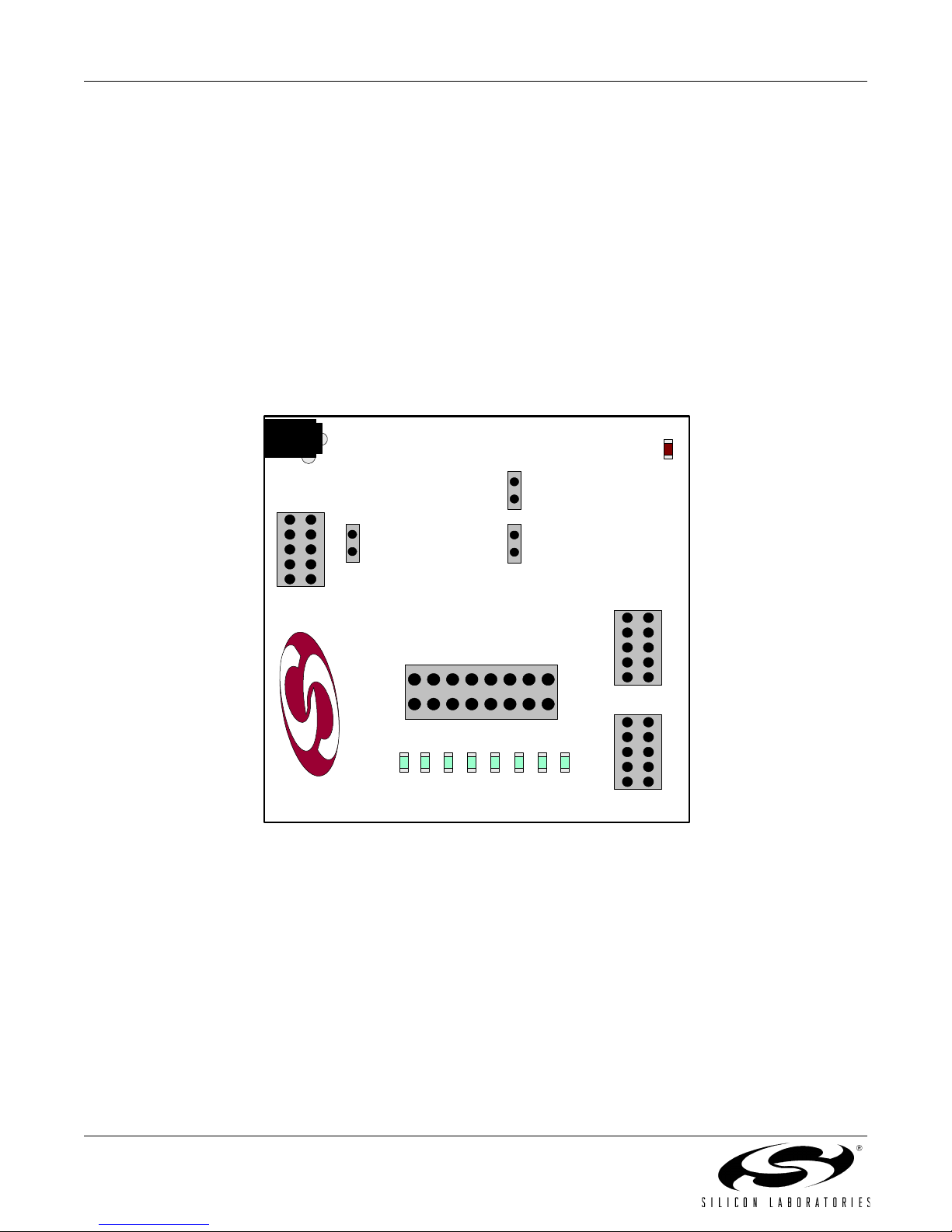
4. Evaluation Board
The CP2120 evaluation board comes with a CP2120 device pre-installed for system evaluation and development.
Numerous I/O connections are provided to facilitate prototyping using the evaluation board. Refer to Figure 2 for
the locations of the various I/O connectors.
J1 Power Connector
J2 SPI Master Interface
J3 SMBus Interface
J4 MISO-MOSI Connector
J6 SMBus SDA Pullup Connector
J7 SMBus SCL Pullup Connector
J9 LED Connector
J10 General Purpose I/O Interface
POWER
J1
J2
J4
J9
D7 D0D1D2D3D4D5D6
SA-TB51PCB
SILICON LABORATORIES
Figure 2. CP2120 Evaluation Board
J6
J7
J3
J10
2 Rev. 0.1
Page 3
CP2120-EK
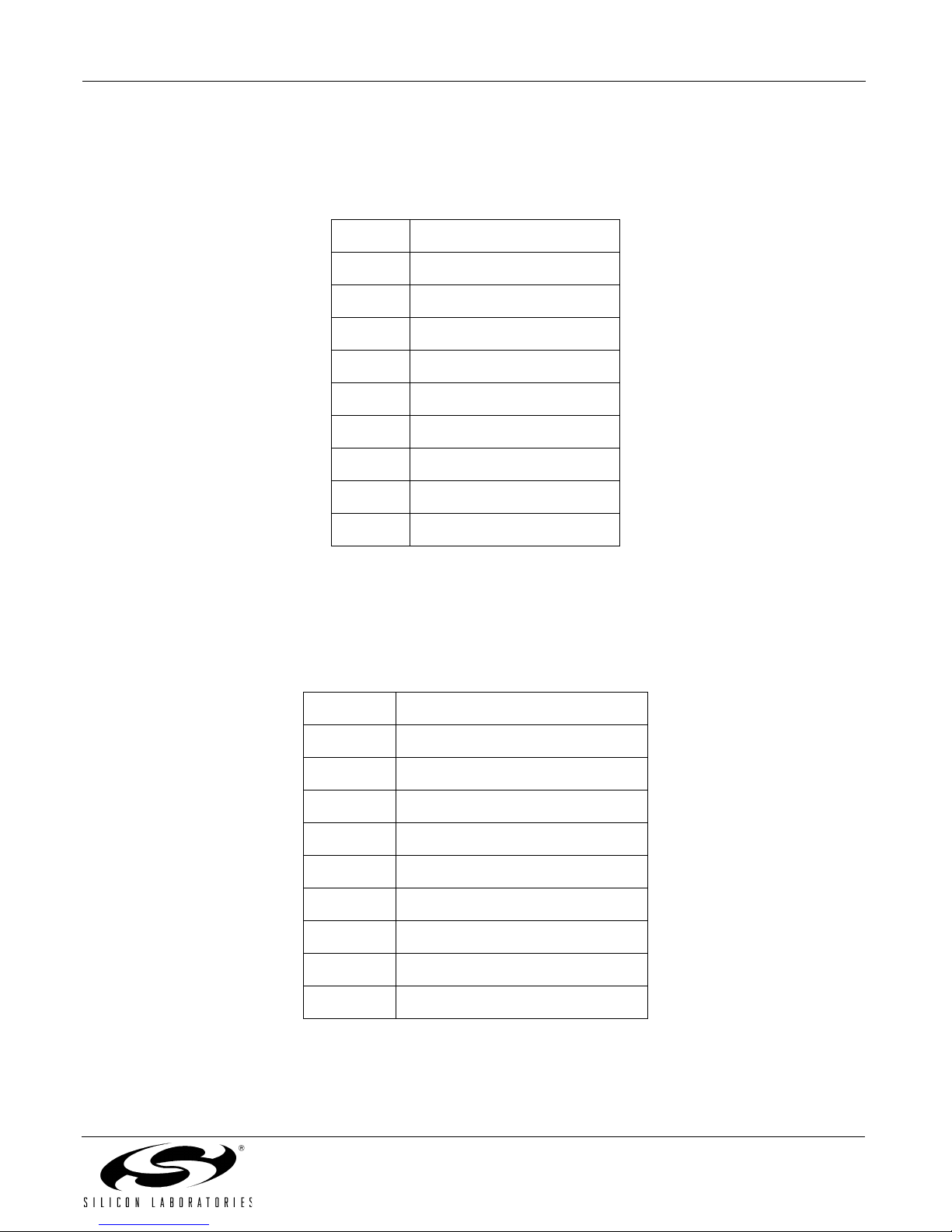
4.1. J2—SPI Master Interface
Connector J2 provides the SPI Master access to the CP2120 SPI, control, and reset lines. Table 1 shows the
pinout of the J2 header.
Table 1. Pinout for J2
Pin 1 SPI Bus—SCLK
Pin 2 SPI Bus—MISO
Pin 3 SPI Bus—MOSI
Pin 4 SPI Bus—CS
Pin 5 INT
Pin 6 Not Used
Pin 7 RST
Pin 8 GND
Pin 9 Not Used
Pin 10 Not Used
4.2. J3—SMBus Interface
Connector J3 provides the CP2120 access to the SMBus. Table 2 shows the pinout of the J3 header.
Note: All pins labeled SCL are tied together, and all pins labeled SDA are tied together. Multiple connections to SCL and SDA
signals are provided to allow multiple devices to connect to the evaluation board.
Table 2. Pinout for J3
Pin 1 SMBus—SCL
Pin 2 SMBus—SDA
Pin 3 SMBus—SCL
Pin 4 SMBus—SDA
Pin 5 SMBus—SCL
Pin 6 SMBus—SDA
Pin 7 SMBus—SCL
Pin 8 SMBus—SDA
Pin 9 GND
Pin 10 GND
Rev. 0.1 3
Page 4

CP2120-EK
4.3. J4—SPI MISO/MOSI Connector
Some SPI master systems tie together the MISO and MOSI SPI data lines. The CP2120 evaluation board allows
developers to connect these two signals through a resistor by placing a header on J4.
Note: When operating the SPI bus with a header on J4, only drive the MOSI pin whenever data is being transmitted to the
CP2120. When the SPI bus is idle, or when the CP2120 is transmitting data, the SPI master must set its MOSI pin into
an open-drain state to avoid port pin contention.
4.4. J6 and J7—SMBus Pullup Connectors
Connectors J6 and J7 give developers the option of adding pullup resistors to the SMBus’s SDA and SCL lines.
Removing shorting blocks from these headers disconnects the pullups from the SMBus lines.
Note: The SMBus lines need pullups to VDD in order to function properly. If the headers are removed from J6 and J7, remem-
ber to add pullups to V
4.5. J9—LED Connector
Connector J9 allows the CP2120’s General Purpose I/O pins to be connected to the array of LEDs on the
evaluation board. Once a header has been placed connecting a pin on the side closest to the CP2120 to its
corresponding pin on the side of the jumper closest to the LEDs. To use one of the LEDs, place a shorting block on
the J9 pin closest to the LED, connecting the corresponding J9 pin on the side of the connector closer to the
CP2120. See Figure 3 for an example of this connection. Writing a 0 to the connected general purpose I/O pin will
turn on the LED, and writing a 1 to that pin will turn off the LED.
elsewhere on the SMBus.
DD
To Control an LED using the CP2120:
Add Shorting Block to LED’s
CP2120
GPIO7
GPIO5
GPIO6
GPIO3
GPIO4
corresponding port pin
Configure port pin to Digital Output
To turn on LED: Set port pin to ‘0’
To turn off LED: Set port pin to ‘1’
Shorting Block placed on
GPIO1, with GPIO1
configured to be Digital
J9
GPIO0
GPIO1
GPIO2
Output and set to ‘0’
Figure 3. Controlling the LEDs
4 Rev. 0.1
Page 5

CP2120-EK
4.6. J10—General Purpose I/O Interface
Connector J10 enables off-board access to the CP2120’s eight general purpose I/O pins, as well as the EdgeTriggered Interrupt Source pin. Table 3 shows the pinout for this header.
Table 3. Pinout for J10
Pin 1 GPIO Pin 0
Pin 2 GPIO Pin 1
Pin 3 GPIO Pin 2
Pin 4 GPIO Pin 3
Pin 5 GPIO Pin 4
Pin 6 GPIO Pin 5
Pin 7 GPIO Pin 6
Pin 8 GPIO Pin 7
Pin 9 Edge Triggered Interrupt Source
Pin 10 GND
Rev. 0.1 5
Page 6

CP2120-EK
5. Schematic
6 Rev. 0.1
Page 7

NOTES:
CP2120-EK
Rev. 0.1 7
Page 8

CP2120-EK
CONTACT INFORMATION
Silicon Laboratories Inc.
400 West Cesar Chavez
Austin, TX 78701
Tel: 1+(512) 416-8500
Fax: 1+(512) 416-9669
Toll Free: 1+(877) 444-3032
Email: MCUinfo@silabs.com
Internet: www.silabs.com
The information in this document is believed to be accurate in all respects at the time of publication but is subject to change without notice.
Silicon Laboratories assumes no responsibility for errors and omissions, and disclaims responsibility for any consequences resulting from
the use of information included herein. Additionally, Silicon Laboratories assumes no responsibility for the functioning of undescribed features
or parameters. Silicon Laboratories reserves the right to make changes without further notice. Silicon Laboratories makes no warranty, representation or guarantee regarding the suitability of its products for any particular purpose, nor does Silicon Laboratories assume any liability
arising out of the application or use of any product or circuit, and specifically disclaims any and all liability, including without limitation consequential or incidental damages. Silicon Laboratories products are not designed, intended, or authorized for use in applications intended to
support or sustain life, or for any other application in which the failure of the Silicon Laboratories product could create a situation where personal injury or death may occur. Should Buyer purchase or use Silicon Laboratories products for any such unintended or unauthorized application, Buyer shall indemnify and hold Silicon Laboratories harmless against all claims and damages.
Silicon Laboratories and Silicon Labs are trademarks of Silicon Laboratories Inc.
Other products or brandnames mentioned herein are trademarks or registered trademarks of their respective holders.
8 Rev. 0.1
 Loading...