

Datasheet C8051F206, C8051F221, C8051F226, C8051F231, C8051F236 Datasheet (Silicon Laboratories)
...Page 1
PRELIMINARY
C8051F206
C8051F220/1/6
C8051F230/1/6
Mixed-Signal 8KB ISP FLASH MCU Family
ANALOG PERIPHERALS
- SAR ADC
• 12-bit Resolution (‘F206)
• 8-Bit Resolution (‘F220/1/6)
• ±1/4 LSB INL (8-bit) and ±2 LSB INL (12-bit)
• Up to 100ksps
• Up to 32 Channel Input Multiplexer; Each Port
I/O Pin can be an ADC Input
- Two Comparators
• 16 Programmable Hysteresis States
• Configurable to Generate Interrupts or Reset
- VDD Monitor and Brown-out Detector
ON-CHIP JTAG DEBUG
- On-Chip Debug Circuitry Facilitates Full Speed, Nonintrusive In-system Debug (No Emulator Required!)
- Provides Breakpoints, Single-Stepping, Watchpoints,
Stack Monitor
- Inspect/Modify Memory and Registers
- Superior Performance to Emulation Systems Using
ICE-Chips, Target Pods, and Sockets
- Complete, Low Cost Development Kit: $99
HIGH SPEED 8051 µµµµC Core
- Pipe-lined Instruction Architecture; Executes 70% of
Instructions in 1 or 2 System Clocks
- Up to 25MIPS Throughput with 25MHz Clock
- Expanded Interrupt Handler
MEMORY
- 256 Bytes Internal Data RAM
- 1024 Bytes XRAM (available on ‘F206/226/236)
- 8k Bytes FLASH; In-System Programmable in 512
byte Sectors
DIGITAL PERIPHERALS
- Four byte wide Port I/O; All are 5V tolerant
- Hardware UART and SPI bus
- 3 General Purpose 16-Bit Counter/Timers
- Dedicated Watch-Dog Timer
- Bi-directional Reset
- System Clock: Internal Programmable Oscillator,
External Crystal, External RC, or External Clock
SUPPLY VOLTAGE .................2.7V to 3.6V
- Typical Operating Current: 10mA @ 25MHz
- Multiple Power Saving Sleep and Shutdown Modes
(48-Pin TQFP and 32-Pin LQFP Version Available)
Temperature Range: –40°°°°Cto+85°°°°C
ANALOG PERIPHERALS
PGA
AMUX
+
-
VOLTAGE
COMPARATORS
SAR
ADC
+
-
DIGITAL I/O
SPI Bus
Timer 0
Timer 1
Timer 2
HIGH-SPEED CONTROLLER CORE
8051 CPU
(25MIPS)
8K x 8
ISP FLASH
CLOCK
CIRCUIT
1280 x 8
SRAM
JTAG
22 INTERRUPTS
Port 0Port 1
UART
Digital MUX
Port 2Port 3
EMULATION
CIRCUITRY
SANITY
CONTROL
Page 1 CYGNAL Integrated Products, Inc. 2001 5.2001; Rev. 1.1
Page 2

PRELIMINARY
C8051F206
C8051F220/1/6
TABLE OF CONTENTS
1. SYSTEM OVERVIEW........................................................................................................5
Table 1.1.1. Product Selection Guide................................................................................................................6
Figure 1.1. C8051F206, C8051F220 and C8051F226 Block Diagram (48 TQFP)........................................... 7
Figure 1.2 C8051F221 Block Diagram (32 LQFP) ...........................................................................................8
Figure 1.3 C8051F230 and C8051F236 Block Diagram (48 TQFP) ................................................................ 9
Figure 1.4 C8051F231 Block Diagram (32 LQFP) .........................................................................................10
1.1. CIP-51
Figure 1.5. Comparison of Peak MCU Throughputs ....................................................................................... 11
Figure 1.6. On-Board Clock and Reset............................................................................................................ 12
1.2. On-Board Memory ................................................................................................................................13
Figure 1.7. On-Board Memory Map................................................................................................................13
1.3. JTAG .....................................................................................................................................................14
Figure 1.8. Debug Environment Diagram........................................................................................................14
1.4. Digital/Analog Configurable I/O ...........................................................................................................15
Figure 1.9. Port I/O Functional Block Diagram .............................................................................................. 15
1.5. Serial Ports ............................................................................................................................................ 15
1.6. Analog to Digital Converter .................................................................................................................. 16
Figure 1.10. ADC Diagram ............................................................................................................................. 16
1.7. Comparators .......................................................................................................................................... 17
Figure 1.11. Comparator Diagram................................................................................................................... 17
2. ABSOLUTE MAXIMUM RATINGS* ............................................................................18
3. GLOBAL DC ELECTRICAL CHARACTERISTICS...................................................18
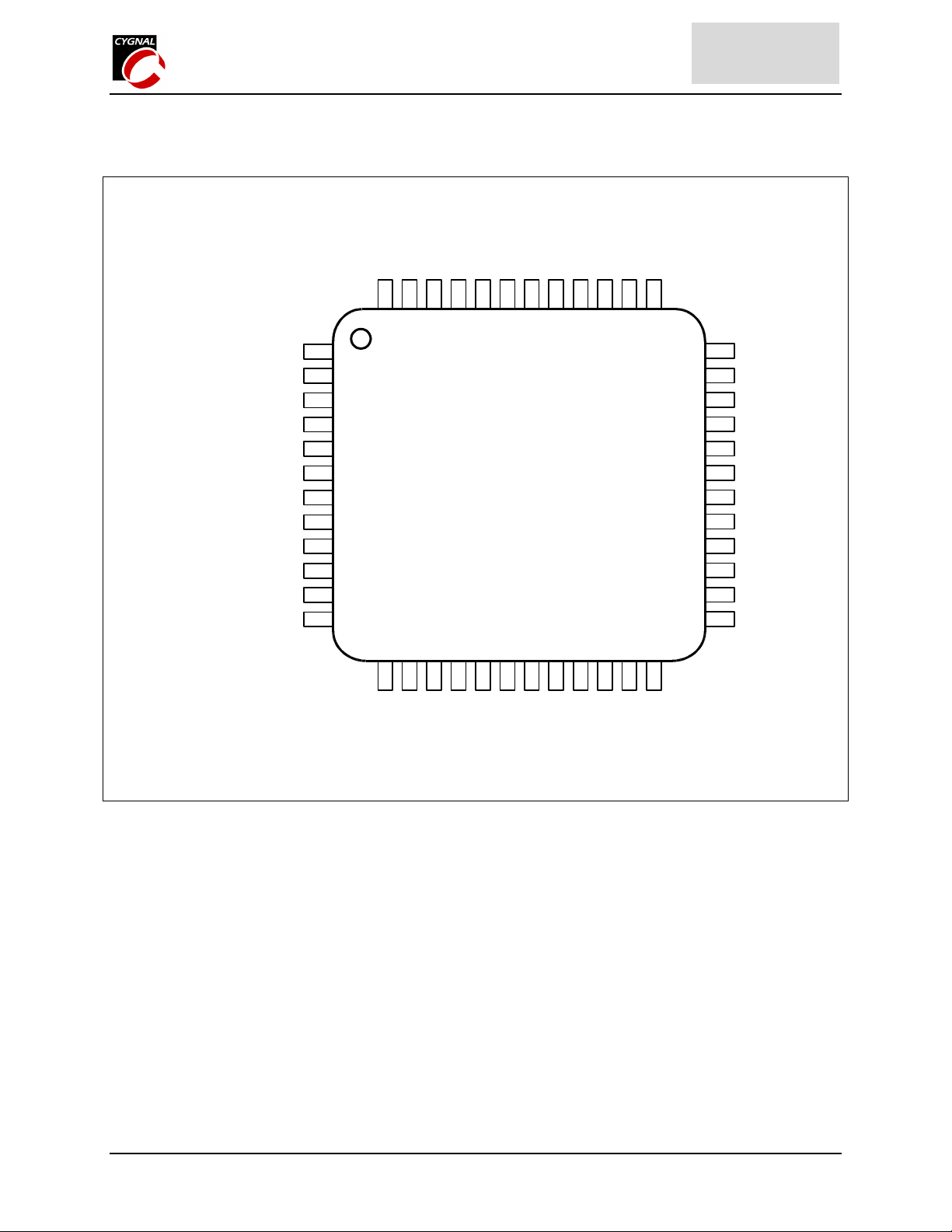
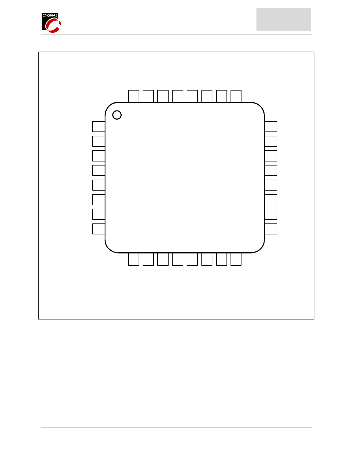
4. PINOUT AND PACKAGE DEFINITIONS.....................................................................19
Table 4.1 Pin Definitions................................................................................................................................. 19
Figure 4.1 TQFP-48 Pin Diagram .................................................................................................................... 21
Figure 4.2 LQFP-32 Pin Diagram .................................................................................................................... 22
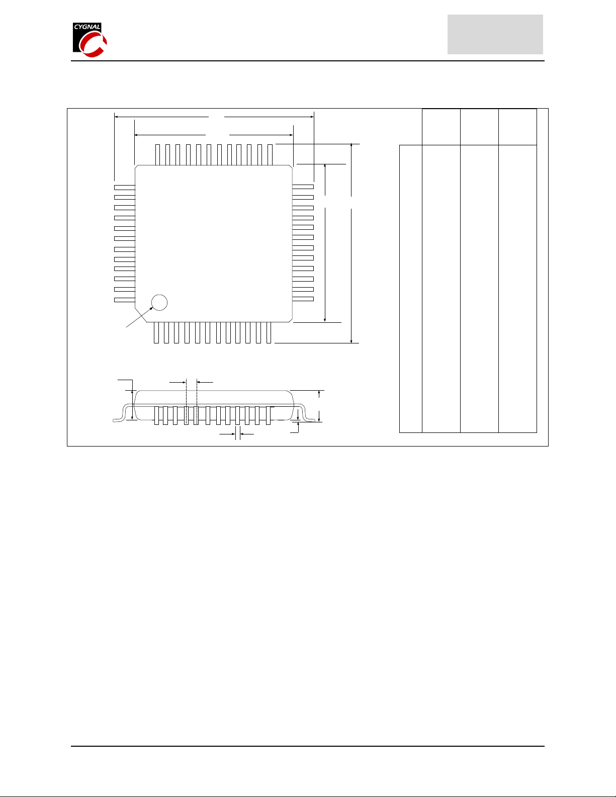
Figure 4.3 TQFP-48 Package Drawing.............................................................................................................23
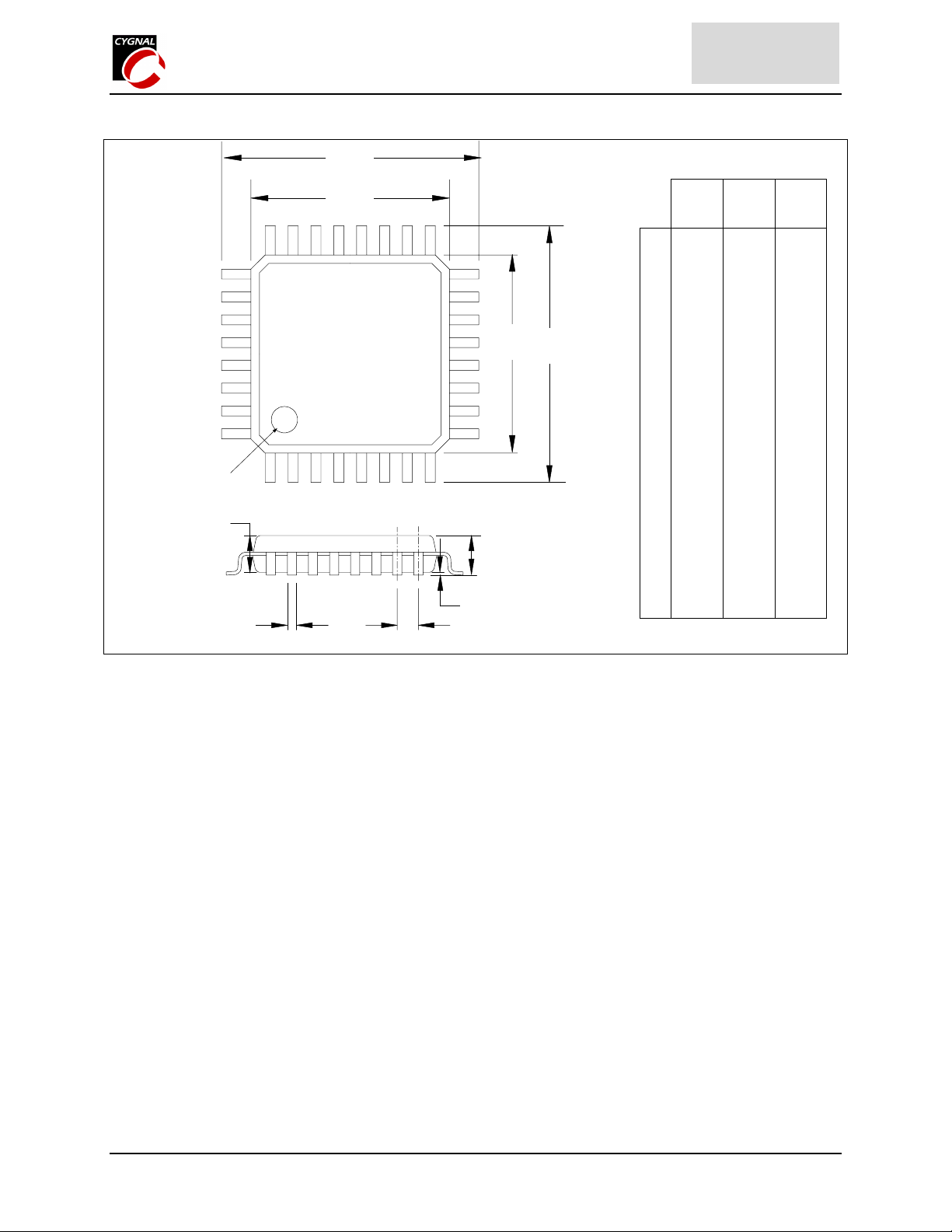
Figure 4.4 LQFP-32 Package Drawing............................................................................................................ 24
5. ADC (8-Bit, C8051F220/1/6 Only) ....................................................................................25
Figure 5.1. 8-Bit ADC Functional Block Diagram.......................................................................................... 25
5.1. Analog Multiplexer and PGA................................................................................................................ 25
5.2. ADC Modes of Operation......................................................................................................................25
Figure 5.2. 12-Bit ADC Track and Conversion Example Timing ...................................................................26
Figure 5.3. AMX0SL: AMUX Channel Select Register (C8051F220/1/6) ..................................................... 27
Figure 5.4. ADC0CF: ADC Configuration Register (C8051F220/1/6) ........................................................... 28
Figure 5.5. ADC0CN: ADC Control Register (C8051F220/1/6) ....................................................................29
Figure 5.6. ADC0H: ADC Data Word Register (C8051F220/1/6).................................................................30
5.3. ADC Programmable Window Detector ................................................................................................. 30
Figure 5.7. ADC0GTH: ADC Greater-Than Data Register (C8051F220/1/6)................................................ 30
Figure 5.8. ADC0LTH: ADC Less-Than Data Byte Register (C8051F220/1/6).............................................30
Figure 5.9. 8-Bit ADC Window Interrupt Examples.......................................................................................31
Table 5.1. 8-Bit ADC Electrical Characteristics.............................................................................................. 32
6. ADC (12-Bit, C8051F206 Only).........................................................................................33
Figure 6.1. 12-Bit ADC Functional Block Diagram........................................................................................33
6.1. Analog Multiplexer and PGA................................................................................................................ 33
6.2. ADC Modes of Operation......................................................................................................................33
Figure 6.2. 12-Bit ADC Track and Conversion Example Timing ...................................................................34
Figure 6.3. AMX0SL: AMUX Channel Select Register (C8051F220/1/6 and C8051F206) ..........................35
Figure 6.4. ADC0CF: ADC Configuration Register (C8051F220/1/6 and C8051F206).................................36
Figure 6.5. ADC0CN: ADC Control Register (C8051F220/1/6 and C8051F206) ..........................................37
Figure 6.6. ADC0H: ADC Data Word MSB Register (C8051F206) ............................................................. 38
TM
Microcontroller Core.............................................................................................................11
Page 2 CYGNAL Integrated Products, Inc. 2001 5.2001; Rev. 1.1
Page 3

PRELIMINARY
C8051F206
C8051F220/1/6
Figure 6.7. ADC0L: ADC Data Word LSB Register (C8051F206) ...............................................................38
6.3. ADC Programmable Window Detector ................................................................................................. 38
Figure 6.8. ADC0GTH: ADC Greater-Than Data High Byte Register (C8051F206) ..................................... 39
Figure 6.9. ADC0GTL: ADC Greater-Than Data Low Byte Register (C8051F206) ......................................39
Figure 6.10. ADC0LTH: ADC Less-Than Data High Byte Register (C8051F206) ........................................ 39
Figure 6.11. ADC0LTL: ADC Less-Than Data Low Byte Register (C8051F206) ......................................... 39
Figure 6.12. 12-Bit ADC Window Interrupt Examples, Right Justified Data.................................................. 40
Figure 6.13. 12-Bit ADC Window Interrupt Examples, Left Justified Data....................................................41
Table 6.1. 12-Bit ADC Electrical Characteristics (C8015F206 only) ............................................................. 42
7. VOLTAGE REFERENCE (C8051F220/1/6) ...................................................................43
Figure 7.1. Voltage Reference Functional Block Diagram.............................................................................. 43
Figure 7.2. REF0CN: Reference Control Register ..........................................................................................44
Table 7.1. Reference Electrical Characteristics...............................................................................................44
8. COMPARATORS ..............................................................................................................45
Figure 8.1. Comparator Functional Block Diagram ........................................................................................ 45
Figure 8.2. Comparator Hysteresis Plot........................................................................................................... 46
Figure 8.3. CPT0CN: Comparator 0 Control Register .................................................................................... 47
Figure 8.4. CPT1CN: Comparator 1 Control Register .................................................................................... 48
Table 8.1. Comparator Electrical Characteristics ............................................................................................ 49
9. CIP-51 MICROCONTROLLER ......................................................................................50
Figure 9.1. CIP-51 Block Diagram.................................................................................................................. 50
9.1. INSTRUCTION SET ............................................................................................................................ 52
Table 9.1. CIP-51 Instruction Set Summary.................................................................................................... 52
9.2. MEMORY ORGANIZATION.............................................................................................................. 56
Figure 9.2. Memory Map................................................................................................................................. 57
9.3. SPECIAL FUNCTION REGISTERS....................................................................................................59
Table 9.2. Special Function Register Memory Map ........................................................................................59
Table 9.3. Special Function Registers ............................................................................................................. 59
Figure 9.3. SP: Stack Pointer........................................................................................................................... 62
Figure 9.4. DPL: Data Pointer Low Byte ........................................................................................................62
Figure 9.5. DPH: Data Pointer High Byte .......................................................................................................62
Figure 9.6. PSW: Program Status Word.......................................................................................................... 63
Figure 9.7. ACC: Accumulator........................................................................................................................64
Figure 9.8. B: B Register.................................................................................................................................64
9.4. INTERRUPT HANDLER ..................................................................................................................... 65
Table 9.4. Interrupt Summary..........................................................................................................................66
Figure 9.9. IE: Interrupt Enable....................................................................................................................... 67
Figure 9.10. IP: Interrupt Priority .................................................................................................................... 68
Figure 9.11. EIE1: Extended Interrupt Enable 1 ............................................................................................. 69
Figure 9.12. EIE2: Extended Interrupt Enable 2 ............................................................................................. 70
Figure 9.13. EIP1: Extended Interrupt Priority 1 ............................................................................................ 71
Figure 9.14. EIP2: Extended Interrupt Priority 2 ............................................................................................ 72
9.5. Power Management Modes ................................................................................................................... 73
Figure 9.15. PCON: Power Control Register .................................................................................................. 74
10. FLASH MEMORY.............................................................................................................75
10.1. Programming The Flash Memory ...................................................................................................... 75
Table 10.1. FLASH Memory Electrical Characteristics..................................................................................75
10.2. Non-volatile Data Storage .................................................................................................................76
10.3. Security Options ................................................................................................................................ 76
Figure 10.1. Flash Program Memory Security Bytes........................................................................................77
Figure 10.2. PSCTL: Program Store RW Control ........................................................................................... 78
Figure 10.3. FLSCL: Flash Memory Timing Prescaler ................................................................................... 79
Figure 10.4. FLACL: Flash Access Limit........................................................................................................79
11. ON-BOARD XRAM (C8051F226/236/206)......................................................................80
Page 3 CYGNAL Integrated Products, Inc. 2001 5.2001; Rev. 1.1
Page 4

PRELIMINARY
C8051F206
C8051F220/1/6
Figure 11.1. EMI0CN: External Memory Interface Control............................................................................ 80
12. RESET SOURCES .............................................................................................................81
Figure 12.1. Reset Sources Diagram ...............................................................................................................81
12.1. Power-on Reset.................................................................................................................................. 82
12.2. Software Forced Reset ....................................................................................................................... 82
Figure 12.2. VDD Monitor Timing Diagram...................................................................................................82
12.3. Power-fail Reset.................................................................................................................................82
12.4. External Reset.................................................................................................................................... 83
12.5. Missing Clock Detector Reset ........................................................................................................... 83
12.6. Comparator 0 Reset ...........................................................................................................................83
12.7. Watchdog Timer Reset ......................................................................................................................83
Figure 12.3. WDTCN: Watchdog Timer Control Register..............................................................................84
Figure 12.4. RSTSRC: Reset Source Register.................................................................................................85
Table 12.1. VDD Monitor Electrical Characteristics ...................................................................................... 86
13. OSCILLATOR ...................................................................................................................87
Figure 13.1. Oscillator Diagram ...................................................................................................................... 87
Figure 13.2. OSCICN: Internal Oscillator Control Register............................................................................ 88
Table 13.1. Internal Oscillator Electrical Characteristics ................................................................................88
Figure 13.3. OSCXCN: External Oscillator Control Register ......................................................................... 89
13.1. External Crystal Example .................................................................................................................. 90
13.2. External RC Example ........................................................................................................................90
13.3. External Capacitor Example .............................................................................................................. 90
14. PORT INPUT/OUTPUT....................................................................................................91
14.1. Port I/O Initialization......................................................................................................................... 91
Figure 14.1. Port I/O Functional Block Diagram ............................................................................................ 92
Figure 14.2. Port I/O Cell Block Diagram.......................................................................................................92
Figure 14.3. PRT0MX: Port I/O MUX Register 0 .......................................................................................... 93
Figure 14.4. PRT1MX: Port I/O MUX Register 1 .......................................................................................... 94
Figure 14.5. PRT2MX: Port I/O MUX Register 2 .......................................................................................... 94
14.2. General Purpose Port I/O...................................................................................................................95
Figure 14.6. P0: Port0 Register ....................................................................................................................... 95
Figure 14.7. PRT0CF: Port0 Configuration Register ...................................................................................... 95
Figure 14.8. P0MODE: Port0 Digital/Analog Input Mode.............................................................................. 96
Figure 14.9. P1: Port1 Register ....................................................................................................................... 96
Figure 14.10. PRT1CF: Port1 Configuration Register .................................................................................... 96
Figure 14.12. PRT1IF: Port1 Interrupt Flag Register ...................................................................................... 97
Figure 14.13. P2: Port2 Register ..................................................................................................................... 98
Figure 14.14. PRT2CF: Port2 Configuration Register .................................................................................... 98
Figure 14.15
Figure 14.16. P3: Port3 Register* ................................................................................................................... 99
Figure 14.17. PRT3CF: Port3 Configuration Register* ..................................................................................99
Figure 14.18. P3MODE: Port3 Digital/Analog Input Mode*.......................................................................... 99
Table 14.1. Port I/O DC Electrical Characteristics........................................................................................100
. P2MODE: Port2 Digital/Analog Input Mode ........................................................................... 98
15. SERIAL PERIPHERAL INTERFACE BUS.................................................................101
Figure 15.1. SPI Block Diagram ................................................................................................................... 101
Figure 15.2. Typical SPI Interconnection...................................................................................................... 102
15.1. Signal Descriptions..........................................................................................................................102
15.2. Operation ......................................................................................................................................... 103
Figure 15.3. Full Duplex Operation............................................................................................................... 103
15.3. Serial Clock Timing.........................................................................................................................104
Figure 15.4. Data/Clock Timing Diagram .....................................................................................................104
15.4. SPI Special Function Registers........................................................................................................105
Figure 15.5. SPI0CFG: SPI Configuration Register ......................................................................................105
Figure 15.6. SPI0CN: SPI Control Register ..................................................................................................106
Page 4 CYGNAL Integrated Products, Inc. 2001 5.2001; Rev. 1.1
Page 5

PRELIMINARY
C8051F206
C8051F220/1/6
Figure 15.7. SPI0CKR: SPI Clock Rate Register ..........................................................................................107
Figure 15.8. SPI0DAT: SPI Data Register .................................................................................................... 107
16. UART.................................................................................................................................108
Figure 16.1. UART Block Diagram .............................................................................................................. 108
16.1. UART Operational Modes...............................................................................................................109
Table 16.1. UART Modes ............................................................................................................................. 109
Figure 16.2. UART Mode 0 Interconnect......................................................................................................109
Figure 16.3. UART Mode 0 Timing Diagram ...............................................................................................109
Figure 16.4. UART Mode 1 Timing Diagram ...............................................................................................110
Figure 16.5. UART Modes 1, 2, and 3 Interconnect Diagram.......................................................................111
Figure 16.6. UART Modes 2 and 3 Timing Diagram.................................................................................... 111
16.2. Multiprocessor Communications..................................................................................................... 112
Figure 16.7. UART Multi-Processor Mode Interconnect Diagram ...............................................................112
Table 16.2. Oscillator Frequencies for Standard Baud Rates ........................................................................ 113
Figure 16.8. SBUF: Serial (UART) Data Buffer Register............................................................................. 113
Figure 16.9. SCON: Serial Port Control Register..........................................................................................114
17. TIMERS ............................................................................................................................115
17.1. Timer 0 and Timer 1........................................................................................................................115
Figure 17.1. T0 Mode 0 Block Diagram .......................................................................................................116
Figure 17.2. T0 Mode 2 Block Diagram .......................................................................................................117
Figure 17.3. T0 Mode 3 Block Diagram .......................................................................................................118
Figure 17.4. TCON: Timer Control Register.................................................................................................119
Figure 17.5. TMOD: Timer Mode Register...................................................................................................120
Figure 17.6. CKCON: Clock Control Register.............................................................................................. 121
Figure 17.7. TL0: Timer 0 Low Byte ............................................................................................................ 122
Figure 17.8. TL1: Timer 1 Low Byte ............................................................................................................ 122
Figure 17.9. TH0: Timer 0 High Byte ........................................................................................................... 122
Figure 17.10. TH1: Timer 1 High Byte ......................................................................................................... 122
17.2. Timer 2 ............................................................................................................................................123
Figure 17.11. T2 Mode 0 Block Diagram .....................................................................................................124
Figure 17.12. T2 Mode 1 Block Diagram .....................................................................................................125
Figure 17.13. T2 Mode 2 Block Diagram .....................................................................................................126
Figure 17.14. T2CON: Timer 2 Control Register..........................................................................................127
Figure 17.15. RCAP2L: Timer 2 Capture Register Low Byte.......................................................................128
Figure 17.16. RCAP2H: Timer 2 Capture Register High Byte......................................................................128
Figure 17.17. TL2: Timer 2 Low Byte .......................................................................................................... 128
Figure 17.18. TH2: Timer 2 High Byte ......................................................................................................... 128
18. JTAG .................................................................................................................................129
Figure 18.1. IR: JTAG Instruction Register ..................................................................................................129
18.1. Flash Programming Commands....................................................................................................... 130
Figure 18.2 FLASHCON: JTAG Flash Control Register .............................................................................. 131
Figure 18.3. FLASHADR: JTAG Flash Address Register ............................................................................. 131
Figure 18.4. FLASHDAT: JTAG Flash Data Register.................................................................................. 132
Figure 18.5. FLASHSCL: JTAG Flash Scale Register.................................................................................. 132
18.2. Boundary Scan Bypass and ID Code ...............................................................................................133
Figure 18.6. DEVICEID: JTAG Device ID Register .................................................................................... 133
18.3. Debug Support.................................................................................................................................133
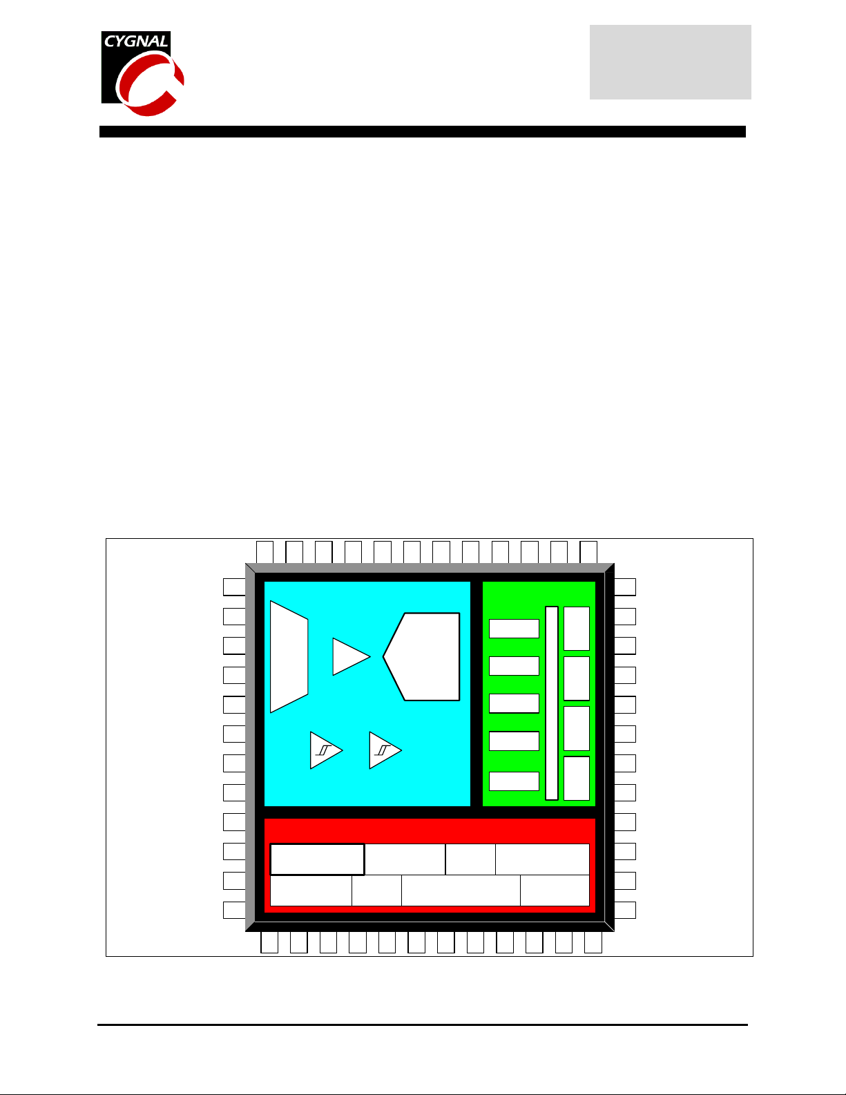
1. SYSTEM OVERVIEW
The C8051F2xx is a family of fully integrated, mixed-signal System on a Chip MCU’s available with a true 8-bit
multi-channel ADC (‘F220/1/6 and ‘F206), or without an ADC (‘F230/1/6). Each model features an 8051compatible microcontroller core with 8kbytes of FLASH memory. There are also UART and SPI serial interfaces
implemented in hardware (not “bit-banged” in user software). Products in this family feature 22 or 32 general
Page 5 CYGNAL Integrated Products, Inc. 2001 5.2001; Rev. 1.1
Page 6
PRELIMINARY
C8051F206
C8051F220/1/6
purpose I/O pins, some of which can be used for assigned digital peripheral interface. Any pins may be configured
for use as analog input to the analog-to-digital converter (‘F220/1/6 and ‘F206 only). (See the Product Selection
Guide in Table 1.1.1 for a quick reference of each MCUs’ feature set.)
Other features include an on-board VDD monitor, WDT, and clock oscillator. On-board FLASH memory can be
reprogrammed in-circuit, and may also be used for non-volatile data storage. Integrated peripherals can also
individually shut down any or all of the peripherals to conserve power. All parts have 256 bytes of SRAM. Also, an
additional 1024 bytes of RAM is available in the ‘F226/’F236.
On-board JTAG debug support allows non-intrusive (uses no on-chip resources), full speed, in-circuit debug using
the production MCU installed in the final application. This debug system supports inspection and modification of
memory and registers, setting breakpoints, watchpoints, single stepping, run and halt commands. All analog and
digital peripherals are fully functional when emulating using JTAG.
Each MCU is specified for 2.7V to 3.6V operation over the industrial temperature range (-45C to +85C) and is
available in the 48-pin TFQP and 32-pin LFQP. The Port I/Os are tolerant for input signals up to 5V.
Table 1.1.1. Product Selection Guide
Part Number
C8051F206 25 8k 1280
C8051F220 25 8k 256
C8051F221 25 8k 256
C8051F226 25 8k 1280
C8051F230 25 8k 256
C8051F231 25 8k 256
C8051F236 25 8k 1280
MIPS (Peak)
FLASH Memory
RAM
√√
√√
√√
√√
√√
√√
√√
SPI
UART
Timers (16-bit)
Digital Port I/O’s
ADC Resolution (bits)
ADC Max Speed (ksps)
ADC Inputs
Voltage Comparators
3 32 12 100 32 2 48TQFP
3 32 8 100 32 2 48TQFP
3 22 8 100 22 2 32LQFP
3 32 8 100 32 2 48TQFP
3 32 - - - 2 48TQFP
3 22 - - - 2 32LQFP
3 32 - - - 2 48TQFP
Package
Page 6 CYGNAL Integrated Products, Inc. 2001 5.2001; Rev. 1.1
Page 7

VDD
VDD
GND
GND
TCK
TMS
TDI
TDO
/RST
VDDMONEN
XTAL1
XTAL2
PRELIMINARY
C8051F206
C8051F220/1/6
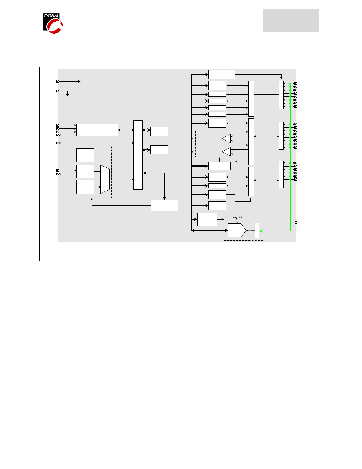
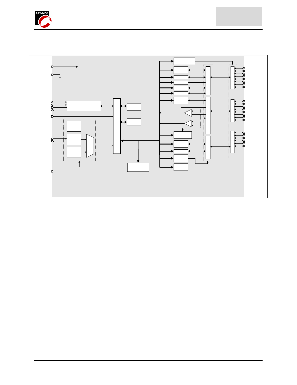
Figure 1.1. C8051F206, C8051F220 and C8051F226 Block Diagram (48 TQFP)
Port I/O Mode
CP0
CP1
ADC
Config. &
Control
& Config.
Port 0
Latch
UART
Timer 0
Timer 1
Timer 2
Port 1
Latch
Comparator
Config.
Port 2
Latch
SPI
Port Mux
Control
Port 3
Latch
P0.0/TX
P0.1/RX
P0.2//INT0
P0.3//INT1
P0.4/T0
P0.5/T1
P0.6/T2
P0.7/T2EX
P1.0/CP0+
P1.1/CP0P1.2/CP0
P1.3/CP1+
P1.4/CP1P1.5/CP1
P1.6/SYSCLK
P1.7
P2.0/SCK
P2.1/MISO
P2.2/MOSI
P2.3/NSS
P2.4
P2.5
P2.6
P2.7
P3.0
P3.1
P3.2
P3.3
P3.4
P3.5
P3.6
P3.7
VREF
AIN0-AIN31
P
0
D
r
v
P
1
D
r
v
P
2
D
r
v
P
3
D
r
v
P
0
M
U
X
P
CP0+
CP0-
CP1+
CP1-
VREF
VREF
1
M
U
X
P
2
M
U
X
A
M
U
X
CP0
CP1
VDD
SAR
ADC
Digital Power
1024 Byte
XRAM
(Available in
8kbyte
FLASH
256 byte
SRAM
SFR Bus
Clock & Reset
Configuration
'F226)
Reset
8
0
5
1
C
o
r
e
JTAG
Emulation HW
Logic
VDD
Monitor,
WDT
External
Oscillator
Circuit
Internal
Oscillator
NC
NC
NC
System Clock
Page 7 CYGNAL Integrated Products, Inc. 2001 5.2001; Rev. 1.1
Page 8
VDD
GND
TCK
TMS
TDI
TDO
/RST
XTAL1
XTAL2
Digital Power
JTAG
Logic
VDD
Monitor,
WDT
External
Oscillator
Circuit
Internal
Oscillator
Emulation HW
PRELIMINARY
Figure 1.2 C8051F221 Block Diagram (32 LQFP)
Port I/O Mode
& Config.
Port 0
Latch
UART
Timer 0
Timer 1
Timer 2
Port 1
Reset
System Clock
8
0
5
1
C
o
r
e
8kbyte
FLASH
256 byte
SRAM
SFR Bus
Clock & Reset
Configuration
CP0
CP1
ADC
Config. &
Control
Latch
Comparator
Config.
Port 2
Latch
SPI
Port Mux
Control
Port 3
Latch
CP0
CP1
VDD
SAR
ADC
CP0+
CP0-
CP1+
CP1-
VREF
VREF
C8051F206
C8051F220/1/6
P0.0/TX
P0.1/RX
P0.2//INT0
P0.3//INT1
P0.4/T0
P0.5/T1
P0.6/T2
P0.7/T2EX
P1.0/CP0+
P1.1/CP0P1.2/CP0
P1.3/CP1+
P1.4/CP1P1.5/CP1
P1.6/SYSCLK
P1.7
P2.0/SCK
P2.1/MISO
P2.2/MOSI
P2.3/NSS
P2.4
P2.5
VREF
AIN0-AIN21
P
0
D
r
v
P
1
D
r
v
P
2
D
r
v
P
0
M
U
X
P
1
M
U
X
P
2
M
U
X
A
M
U
X
Page 8 CYGNAL Integrated Products, Inc. 2001 5.2001; Rev. 1.1
Page 9
VDD
GND
GND
TCK
TMS
TDI
TDO
/RST
MONEN
XTAL1
XTAL2
NC
NC
NC
NC
NC
Digital P ower
PRELIMINARY
Figure 1.3 C8051F230 and C8051F236 Block Diagram (48 TQFP)
Port I/O Mode
& Config.
Port 0
Latch
UART
Timer 0
Timer 1
Timer 2
Port 1
Latch
CP0
CP1
Comparator
Config.
Port 2
Latch
SPI
Port Mux
Control
Port 3
Latch
CP0+
CP0
CP0-
CP1+
CP1
CP1-
JTAG
Logic
VDD
Monitor,
WDT
External
Oscillator
Circuit
Internal
Oscillator
Emulation HW
Reset
System Clock
8
0
5
1
C
SFR Bus
o
r
e
1024 Byte
XRAM
(Available in
'F236)
8kbyte
FLASH
256 byte
SRAM
Clock & Reset
Configuration
C8051F220/1/6
P
0
M
U
X
P
1
M
U
X
P
2
M
U
X
C8051F206
P
0
D
v
P
1
D
v
P
2
D
v
P
3
D
v
P0.0/TX
P0.1/RX
P0.2//INT0
P0.3//INT1
P0.4/T0
P0.5/T1
r
P0.6/T2
P0.7/T2EX
P1.0/CP0+
P1.1/CP0P1.2/CP0
P1.3/CP1+
P1.4/CP1P1.5/CP1
r
P1.6/SYSCLK
P1.7
P2.0/SCK
P2.1/MISO
P2.2/MOSI
P2.3/NSS
P2.4
P2.5
r
P2.6
P2.7
P3.0
P3.1
P3.2
P3.3
P3.4
P3.5
r
P3.6
P3.7
Page 9 CYGNAL Integrated Products, Inc. 2001 5.2001; Rev. 1.1
Page 10
VDD
GND
TCK
TMS
TDI
TDO
/RST
XTAL1
XTAL2
PRELIMINARY
C8051F206
C8051F220/1/6
Figure 1.4 C8051F231 Block Diagram (32 LQFP)
Port I /O Mod e
Digital Power
Reset
8
0
5
1
C
o
r
e
8kbyte
FLASH
256 byte
SRAM
SFR Bus
Clock & Reset
Configurati on
JTAG
Emulation HW
Logic
VDD
Monitor,
WDT
External
Oscillator
Circuit
Internal
Oscillator
NC
System Clock
& Config.
Port 0
Latch
UART
Timer 0
Timer 1
Timer 2
Port 1
Latch
CP0
CP1
Comparator
Config.
Port 2
Latch
SPI
Port Mux
Control
Port 3
Latch
P
0
M
U
X
P
CP0+
CP0-
CP1+
CP1-
1
M
U
X
P
2
M
U
X
CP0
CP1
P
0
D
r
v
P
1
D
r
v
P
2
D
r
v
P0.0/TX
P0.1/RX
P0.2//INT0
P0.3//INT1
P0.4/T0
P0.5/T1
P0.6/T2
P0.7/T2EX
P1.0/CP0+
P1.1/CP0P1.2/CP0
P1.3/CP1+
P1.4/CP1P1.5/CP1
P1.6/SYSCLK
P1.7
P2.0/SCK
P2.1/MISO
P2.2/MOSI
P2.3/NSS
P2.4
P2.5
Page 10 CYGNAL Integrated Products, Inc. 2001 5.2001; Rev. 1.1
Page 11
PRELIMINARY
C8051F206
C8051F220/1/6
1.1. CIP-51TMMicrocontroller Core
1.1.1. Fully 8051 Compatible
The C8051F206, C8051F220/1/6 and C8051F230/1/6 utilize Cygnal’s proprietary CIP-51 microcontroller core. The
CIP-51 is fully compatible with the MCS-51
used to develop software. The core contains the peripherals included with a standard 8052, including three 16-bit
counter/timers, a full-duplex UART, 256 bytes of internal RAM, an optional 1024 bytes of XRAM, 128 byte Special
Function Register (SFR) address space, and four byte-wide I/O Ports.
1.1.2. Improved Throughput
The CIP-51 employs a pipelined architecture that greatly increases its instruction throughput over the standard 8051
architecture. In a standard 8051, all instructions except for MUL and DIV take 12 or 24 system clock cycles to
execute with a maximum system clock of 12MHz. By contrast, the CIP-51 core executes 70% of its instructions in
one or two system clock cycles, with only four instructions taking more than four system clock cycles.
The CIP-51 has a total of 109 instructions. The number of instructions versus the system clock cycles to execute
them is as follows:
TM
instruction set. Standard 803x/805x assemblers and compilers can be
Instructions
Clocks to Execute
265051473121
1 2 2/3 3 3/4 4 4/5 5 8
With the CIP-51’s maximum system clock at 25MHz, it has a peak throughput of 25MIPS. Figure 1.5 shows a
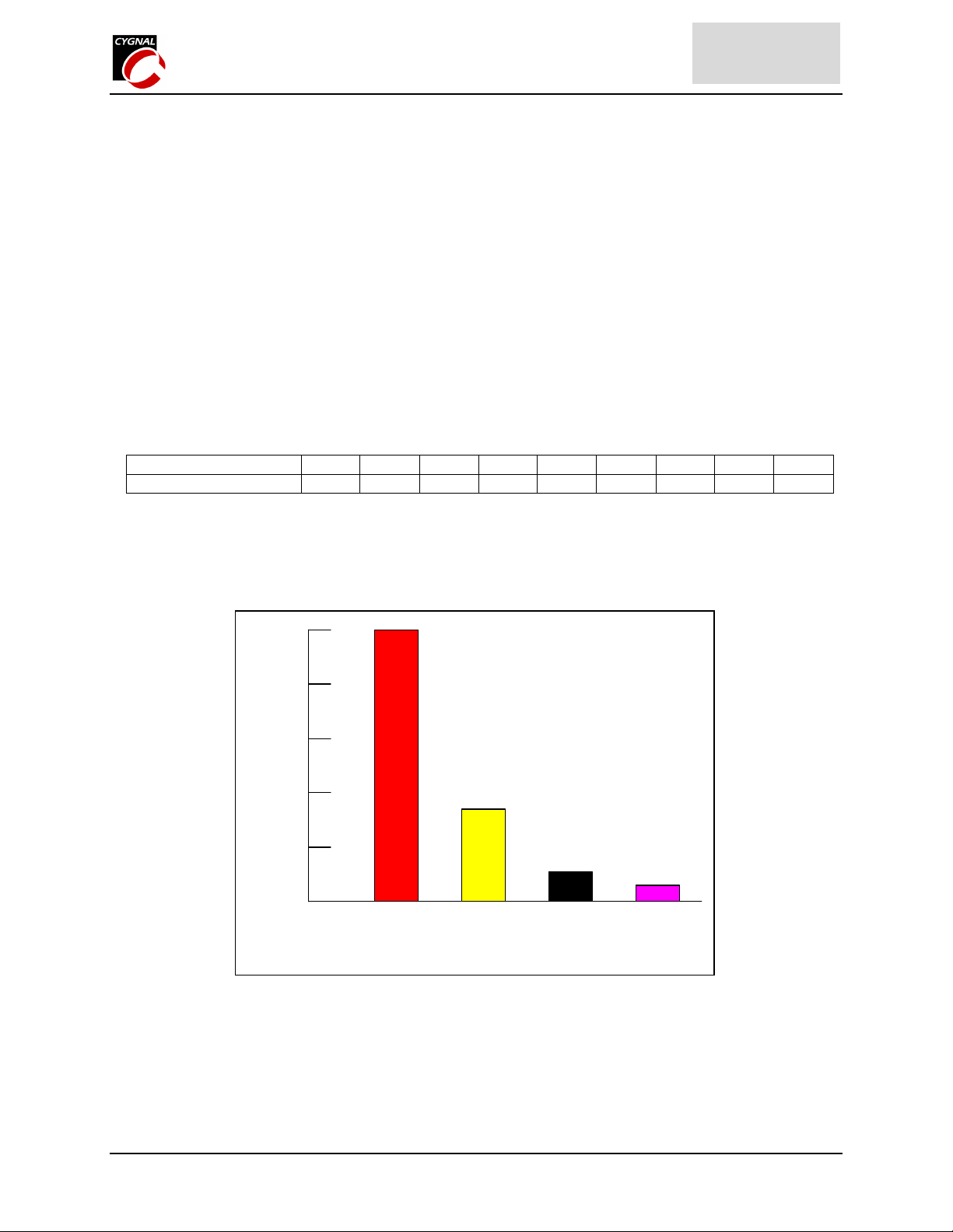
comparison of peak throughputs of various 8-bit microcontroller cores with their maximum system clocks.
Figure 1.5. Comparison of Peak MCU Throughputs
25
20
15
MIPS
10
5
Cygnal
CIP-51
(25MHz clk)
Microchip
PIC17C75x
(33MHz clk)
Philips
80C51
(33MHz clk)
ADuC812
8051
(16MHz clk)
Page 11 CYGNAL Integrated Products, Inc. 2001 5.2001; Rev. 1.1
Page 12
PRELIMINARY
C8051F206
C8051F220/1/6
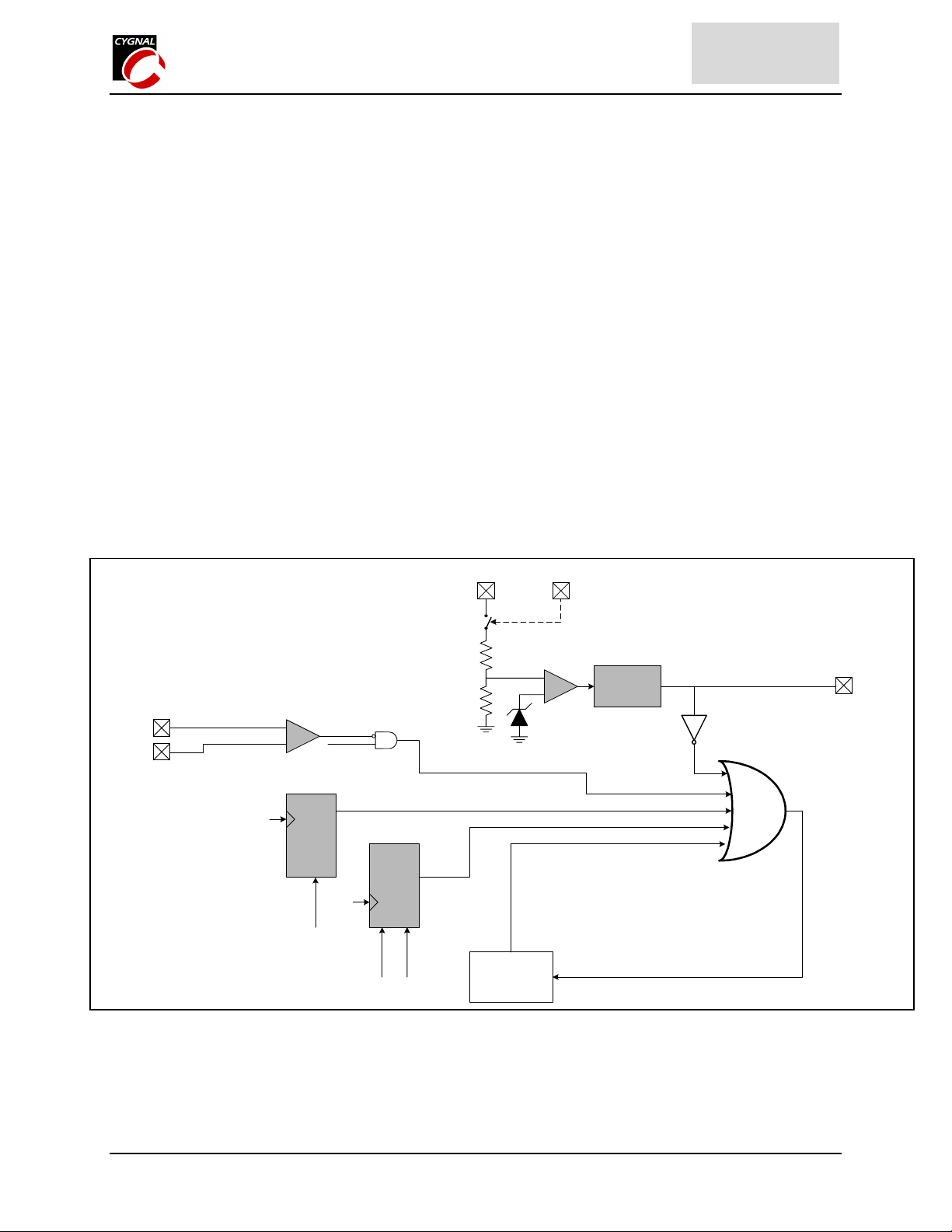
1.1.3. Additional Features
The C8051F206, C8051F220/1/6 and C8051F230/1/6 have several key enhancements both inside and outside the
CIP-51 core to improve overall performance and ease of use in end applications.
The extended interrupt handler provides 22 interrupt sources into the CIP-51 (as opposed to 7 for the standard 8051),
allowing the numerous analog and digital peripherals to interrupt the controller. (An interrupt driven system requires
less intervention by the MCU, giving it more effective throughput.) The extra interrupt sources are very useful when
building multi-tasking, real-time systems.
There are up to six reset sources for the MCU: an on-board VDD monitor, a Watchdog Timer, a missing clock
detector, a voltage level detection from Comparator 0, a forced software reset, and an external reset pin. The /RST
pin is bi-directional, accommodating an external reset, or allowing the internally generated reset to be output on the
/RST pin. The on-board VDD monitor is enabled by pulling the MONEN pin high (digital 1). The user may disable
each reset source except for the VDD monitor and Reset Input Pin from software. The watchdog timer may be
permanently enabled in software after a power-on reset during MCU initialization.
The MCU has an internal, stand-alone clock generator that is used by default as the system clock after reset. If
desired, the clock source may be switched “on the fly” to the external oscillator, which can use a crystal, ceramic
resonator, capacitor, RC, or external clock source to generate the system clock. This can be extremely useful in low
power applications, allowing the MCU to run from a slow (power saving) external crystal source, while periodically
switching to the fast (up to 16MHz) internal oscillator as needed.
CP0+
CP0-
System
Clock
Comparator 0
+
-
Missing
Clock
Detector
EN
MCD
Enable
Figure 1.6. On-Board Clock and Reset
C0RSEF
VDD
WDT
PRE
EN
WDT
WDT
Enable
Strobe
CIP-51
MonEn
Supply
Monitor
+
-
SWRSF
(Software Reset)
System Reset
Core
Supply
Reset
Timeout
(wired-OR)
Reset
Funnel
/RST
Page 12 CYGNAL Integrated Products, Inc. 2001 5.2001; Rev. 1.1
Page 13
PRELIMINARY
C8051F206
C8051F220/1/6
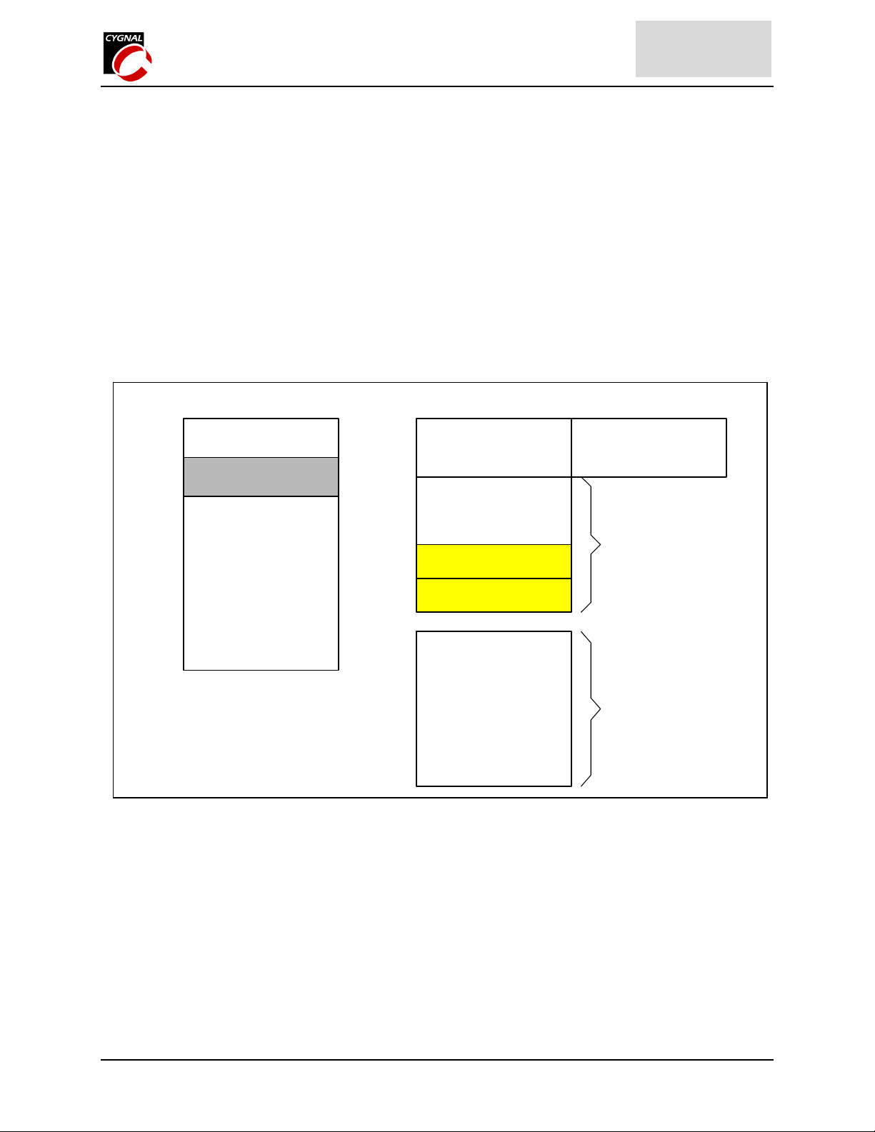
1.2. On-Board Memory
The CIP-51 has a standard 8051 program and data address configuration. It includes 256 bytes of data RAM, with
the upper 128 bytes dual-mapped. An optional 1024 bytes of XRAM is available on the ‘F206, ‘F226 and ‘F236.
Indirect addressing accesses the upper 128 bytes of general purpose RAM, and direct addressing accesses the 128byte SFR address space. The lower 128 bytes of RAM are accessible via direct or indirect addressing. The first 32
bytes are addressable as four banks of general purpose registers, and the next 16 bytes can be byte addressable or bit
addressable.
The MCU’s program memory consists of 8k + 128 bytes of FLASH. This memory may be reprogrammed in-system
in 512 byte sectors, and requires no special off-chip programming voltage. The 512 bytes from addresses 0x1E00 to
0x1FFF are reserved for factory use. There is also a user programmable 128-byte sector at address 0x2000 to
0x207F, which may be useful as a table for storing software constants, nonvolatile configuration information, or as
additional program space. See Figure 1.7 for the MCU system memory map.
Figure 1.7. On-Board Memory Map
0x207F
0x2000
0x1FFF
0x1E00
0x1DFF
0x0000
PROGRAM MEMORY
128 Byte ISP FLASH
RESERVED
FLASH
(In-System
Programmable in 512
Byte Sectors)
0xFF
0x80
0x7F
0x30
0x2F
0x20
0x1F
0x00
0x3FF
0x000
DATA MEMORY
Upper 128 RAM
(Indirect Addressing
Only)
(Direct and Indirect
Addressing)
Bit Addressable
General Purpose
Registers
1024 Byte
XRAM
Special Function
Register's
(Direct Addressing Only)
Lower 128 RAM
(Direct and Indirect
Addressing)
Mapped into
External Data Memory
Space
(C8051F226/236/206 only)
Page 13 CYGNAL Integrated Products, Inc. 2001 5.2001; Rev. 1.1
Page 14
PRELIMINARY
C8051F206
C8051F220/1/6
1.3. JTAG
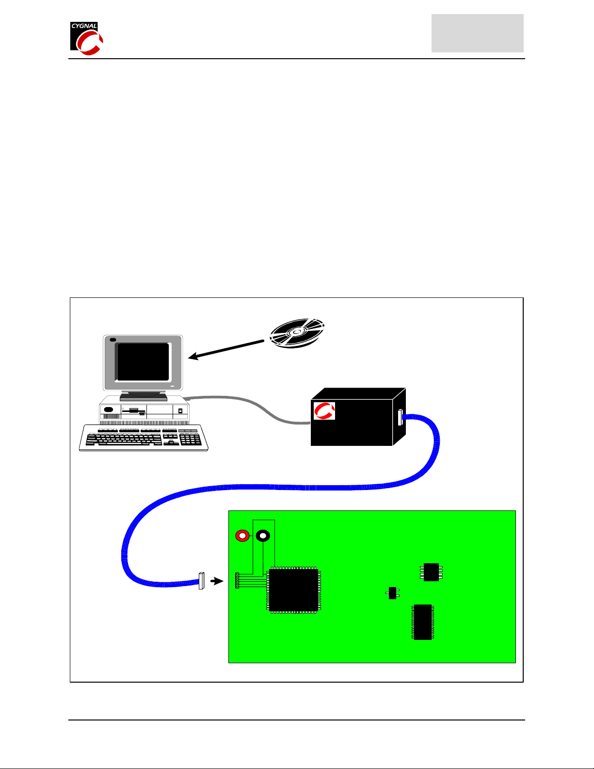
The C8051F2xx have on-chip JTAG and debug logic that provide non-intrusive, full speed, in-circuit debug using
the production part installed in the end application using the four-pin JTAG I/F. The C8051F2xxDK is a
development kit with all the hardware and software necessary to develop application code and perform in-circuit
debug with the C8051F2xx. The kit includes software with a developer’s studio and debugger, an integrated 8051
assembler, and an RS-232 to JTAG interface module referred to as the EC. It also has a target application board
with a C8051F2xx installed and large prototyping area, plus the RS-232 and JTAG cables, and wall-mount power
supply. The Development Kit requires a Windows 9x, NT, or ME computer with one available RS-232 serial port.
As shown in Figure 1.8, the PC is connected via RS-232 to the EC. A six-inch ribbon cable connects the EC to the
user’s application board, picking up the four JTAG pins and VDD and GND. The EC takes its power from the
application board. It requires roughly 20mA at 2.7-3.6V. For applications where there is not sufficient power
available from the target board, the provided power supply can be connected directly to the EC.
This is a vastly superior configuration for developing and debugging embedded applications compared to standard
MCU Emulators, which use on-board “ICE Chips” and target cables and require the MCU in the application board to
be socketed. Cygnal’s debug environment both increases ease of use, and preserves the performance of the precision
analog peripherals.
Figure 1.8. Debug Environment Diagram
WINDOWS 95/98/NT/ME
CYGNAL Integrated
Development Environment
RS-232
EMULATION
CARTRIDGE
JTAG(x4),VDD,GND
VDD GND
C8051
F2XX
TARGET PCB
Page 14 CYGNAL Integrated Products, Inc. 2001 5.2001; Rev. 1.1
Page 15
PRELIMINARY
C8051F206
C8051F220/1/6
1.4. Digital/Analog Configurable I/O
The standard 8051 Ports (0, 1, 2, and 3) are available on the device. The ports behave like standard 8051 ports with
a few enhancements.
Each port pin can be configured as either a push-pull or open-drain output. Any input that is configured as an analog
input will have its corresponding weak pull-up turned off.
Digital resources (timers, SPI, UART, system clock, and comparators) are routed to corresponding I/O pins by
configuring the port multiplexer. Port multiplexers are programmed by setting bits in SFR’s (please see Section 14).
Any of the 32 external port pins may be configured as either analog inputs or digital I/O (See Figure 1.9), so
effectively, all port pins are dual function.
Figure 1.9. Port I/O Functional Block Diagram
PRTnCF &
PnMODE
registers
Port0 I/O Cell
External
pins
P0.0/TX
P0.1/RX
P0.2/INT0
P0.3/INT1
P0.4/T0
P0.5/T1
P0.6/T2
P0.7/T2EX
T0,T1,
T2
Timers
UART
External
INT0 &
INT1
PRTnMX
Registers
Port
0
MUX
P1.0/CP0+
P1.1/CP0P1.2/CP0
P1.3/CP1+
P1.4/CP1P1.5/CP1
P1.6/SYSCK
P1.7
Any port pin ma y be
configur ed via software as an
analog input to the ADC
P2.0/SCK
P2.1/MISO
P2.2/MOSI
P2.3/NSS
P2.4
P2.5
P2.6
P2.7
P3.0
P3.1
P3.2
P3.3
P3.4
P3.5
P3.6
P3.7
SYSCLK
Comparators
0&1
SPI
ADC
Port
1
MUX
Port
2
MUX
A
M
U
X
Port1 I/O Cell
Port2 I/O Cell
Port3 I/O Cell
1.5. Serial Ports
The C8051F206, C8051F220/1/6 and C8051F230/1/6 include a Full-Duplex UART and SPI Bus. Each of the serial
buses is fully implemented in hardware and makes extensive use of the CIP-51’s interrupts, thus requiring very little
intervention by the CPU. The serial buses do not have to “share” resources such as timers, interrupts, or Port I/O, so
both of the serial buses may be used simultaneously. (You may use Timer1, Timer 2, or SYSCLK to generate baud
rates for UART).
Page 15 CYGNAL Integrated Products, Inc. 2001 5.2001; Rev. 1.1
Page 16
PRELIMINARY
C8051F206
C8051F220/1/6
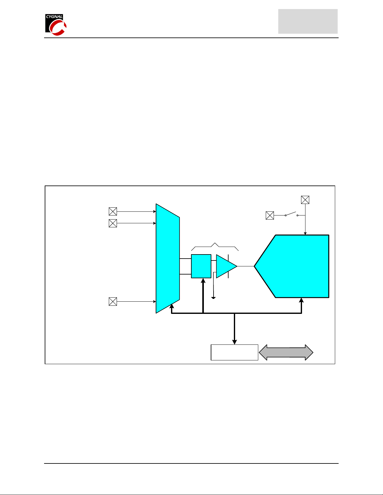
1.6. Analog to Digital Converter
The C8051F220/1/6 has an on-chip 8-bit SAR ADC and the C8051F206 has a 12-bit SAR ADC with a
programmable gain amplifier. With a maximum throughput of 100ksps, the ADC offers true 8-bit with an INL of
±1/4 LSB, and or 12-bit accuracy with ±2 LSB. The voltage reference can be the power supply (VDD), or an
external reference voltage (VREF). Also, the system controller can place the ADC into a power-saving shutdown
mode when not in use. A programmable gain amplifier follows the analog multiplexer. The gain can be set in
software from 0.5 to 16 in powers of 2.
Conversions can be initiated in two ways; a software command or an overflow on Timer 2. This flexibility allows
the start of conversion to be triggered by software events, or convert continuously. A completed conversion causes
an interrupt, or a status bit can be polled in software to determine the end of conversion. The resulting 8-bit data
word is latched into an SFR upon completion of a conversion.
ADC data is continuously monitored by a programmable window detector, which interrupts the CPU when data is
within the user-programmed window. This allows the ADC to monitor key system voltages in background mode,
without the use of CPU resources.
Figure 1.10. ADC Diagram
VREF
AIN0
AIN1
AIN0-31 are port 0-3
pins -- any external
port pin may be configured as
an analog input
(only 22 input port pins on
'F221)
AIN31
...
32-to-1
AMUX
Programmable
Gain Amp
+
X
-
GND
Control & Data
SFR's
VDD
100ksps
SAR
ADC
SFR Bus
Page 16 CYGNAL Integrated Products, Inc. 2001 5.2001; Rev. 1.1
Page 17
PRELIMINARY
C8051F206
C8051F220/1/6
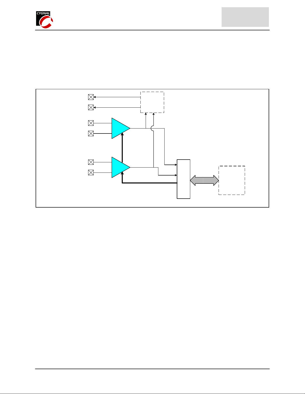
1.7. Comparators
The MCU’s have two on-chip voltage comparators. The inputs of the comparators are available at package pins as
illustrated in Figure 1.11. Each comparator’s hysteresis is software programmable via special function registers
(SFR’s). Both voltage level and positive/negative going symmetry can be easily programmed by the user.
Additionally, comparator interrupts can be implemented on either rising or falling-edge output transitions. Please
see section 8 for details.
Figure 1.11. Comparator Diagram
P1.2
P1.5
P1.0
P1.1
P1.3
P1.4
CP0
CP1
+
CP0
-
+
CP1
-
Port1
MUX
CP0
CP1
SFR's
(Data
and
Cntrl)
CIP-51
and
Interrupt
Handler
Page 17 CYGNAL Integrated Products, Inc. 2001 5.2001; Rev. 1.1
Page 18

PRELIMINARY
C8051F206
C8051F220/1/6
2. ABSOLUTE MAXIMUM RATINGS*
Ambient temperature under bias................................................................................................................. -55 to 125°C
Storage Temperature .................................................................................................................................. -65 to 150°C
Voltage on any Pin (except VDD and Port I/O) with respect to DGND ................................... -0.3V to (VDD + 0.3V)
Voltage on any Port I/O Pin or /RST with respect to DGND .................................................................... -0.3V to 5.8V
Voltage on VDD with respect to DGND ................................................................................................... -0.3V to 4.2V
Total Power Dissipation ......................................................................................................................................... 1.0W
Maximum output current sink by any Port pin .................................................................................................... 200mA
Maximum output current sink by any other I/O pin............................................................................................... 25mA
Maximum output current sourced by any Port pin............................................................................................... 200mA
Maximum output current sourced by any other I/O pin......................................................................................... 25mA
*Note: Stresses above those listed under “Absolute Maximum Ratings” may cause permanent damage to the device.
This is a stress rating only and functional operation of the devices at those or any other conditions above those
indicated in the operation listings of this specification is not implied. Exposure to maximum rating conditions for
extended periods may affect device reliability.
3. GLOBAL DC ELECTRICAL CHARACTERISTICS
-40°Cto+85°C unless otherwise specified.
PARAMETER CONDITIONS MIN TYP MAX UNITS
Power supply voltage (Note 1) 2.7 3.6 V
VDD supply current with
ADC and comparators
active, and CPU active
VDD supply current with
ADC and comparators
active, and CPU inactive
(Idle Mode).
VDD supply current with
ADC and comparators
inactive, and CPU active
Digital Supply Current with
CPU inactive (Idle Mode)
Digital Supply Current (Stop
mode), VDD monitor
enabled.
Digital Supply Current (Stop
Mode), VDD monitor
disabled
Digital Supply RAM Data
Retention Voltage
Specified Operating
Temperature Range
Clock=25MHz
Clock=1MHz
Clock=32kHz
Clock=25MHz
Clock=1MHz
Clock=32kHz
Clock=25MHz
Clock=1MHz
Clock=32kHz
Clock=25MHz
Clock=1MHz
Clock=32kHz
Oscillator not running 10
Oscillator not running 0.1
-40 +85
9.5
3.6
125
1.8
125
20
4.5
0.1
10
1.5 V
mA
µA
5
9
1
mA
µA
mA
µA
mA
µA
µA
µA
°C
Note 1: Power Supply must be greater than 1V and the MONEN pin must be pulled high for VDD monitor to
operate.
Page 18 CYGNAL Integrated Products, Inc. 2001 5.2001; Rev. 1.1
Page 19

PRELIMINARY
4. PINOUT AND PACKAGE DEFINITIONS
Table 4.1 Pin Definitions
‘F220,
226,
‘F221,
Name
VDD
230,
236
48-Pin 32-Pin
11,318
231
Type Description
Digital Voltage Supply.
C8051F206
C8051F220/1/6
GND
MONEN
TCK
TMS
TDI
TDO
XTAL1
XTAL2
/RST
VREF
CP0+
CP0CP0
CP1+
CP1CP1
P0.0/
TX
P0.1/
RX
P0.2/
INT0
P0.3/
INT1
P0.4/
T0
P0.5/
T1
P0.6/
T2
P0.7/
T2EX
P1.0/
CP0+
5,6,
9
8,
13,
32
12
25 17
26 18
28 20
27 19
96
10 7
14 10
75
44
33
22
11
48 32
47 31
40 28
39 27
38 26
37 25
36 24
35 23
34 22
33 21
44
DIn
DIn
DIn
DIn
D Out
AIn
A Out
D I/O
A I/O
AIn
AIn
D Out
AIn
AIn
D Out
D I/O
AIn
D I/O
AIn
D I/O
AIn
D I/O
AIn
D I/O
AIn
D I/O
AIn
D I/O
AIn
D I/O
AIn
D I/O
AIn
Ground. (Note: Pins 5,6, and 8 on the 48-pin package are not connected
(NC), but it is recommended that they be connected to ground.)
Monitor Enable (on 48 pin package ONLY). Enables reset voltage monitor
function when pulled high (logic “1”).
JTAG Test Clock with internal pull-up.
JTAG Test-Mode Select with internal pull-up.
JTAG Test Data Input with internal pull-up. TDI is latched on a rising edge of
TCK.
JTAG Test Data Output. Data is shifted out on TDO on the falling edge of
TCK. TDO output is a tri-state driver.
Crystal Input. This pin is the return for the internal oscillator circuit for a
crystal or ceramic resonator. For a precision internal clock, connect a crystal
or ceramic resonator from XTAL1 to XTAL2. If overdriven by an external
CMOS clock, this becomes the system clock.
Crystal Output. This pin is the excitation driver for a crystal or ceramic
resonator.
Chip Reset. Open-drain output of internal Voltage Supply monitor. Is driven
low when VDD is < 2.7V and MONEN=1, or when a ‘1’is written to PORSF.
An external source can force a system reset by driving this pin low.
Voltage Reference. When configured as an input, this pin is the voltage
reference for the ADC. Otherwise, VDD will be the reference. NOTE: this
pin is Not Connected (NC) on ‘F230/1/6.
Comparator 0 Non-Inverting Input.
Comparator 0 Inverting Input.
Comparator 0 Output
Comparator 1 Non-Inverting Input.
Comparator 1 Inverting Input.
Comparator 1 Output
Port0 Bit0. (See the Port I/O Sub-System section for complete description).
Port0 Bit1. (See the Port I/O Sub-System section for complete description).
Port0 Bit2. (See the Port I/O Sub-System section for complete description).
Port0 Bit3. (See the Port I/O Sub-System section for complete description).
Port0 Bit4. (See the Port I/O Sub-System section for complete description).
Port0 Bit5. (See the Port I/O Sub-System section for complete description).
Port0 Bit6. (See the Port I/O Sub-System section for complete description).
Port0 Bit7. (See the Port I/O Sub-System section for complete description).
Port1 Bit0. (See the Port I/O Sub-System section for complete description).
Page 19 CYGNAL Integrated Products, Inc. 2001 5.2001; Rev. 1.1
Page 20

Name
P1.1/
CP0P1.2/
CP0
P1.3/
CP1+
P1.4/
CP1P1.5/
CP1
P1.6/
SYSCLK
P1.7
P2.0/
SCK
P2.1/
MISO
P2.2/
MOSI
P2.3/
NSS
P2.4
P2.5
P2.6
P2.7
P3.0
P3.1
P3.2
P3.3
P3.4
P3.5
P3.6
P3.7
‘F220,
226,
‘F221,
230,
236
48-Pin 32-Pin
231
33
22
11
48 32
47 31
46 30
45 29
24 16
23 15
22 14
21 13
15 11
16 12
17
18
44
43
42
41
30
29
20
19
PRELIMINARY
Type Description
D I/O
AIn
D I/O
AIn
D I/O
AIn
D I/O
AIn
D I/O
AIn
D I/O
AIn
D I/O
AIn
D I/O
AIn
D I/O
AIn
D I/O
AIn
D I/O
AIn
D I/O
AIn
D I/O
AIn
D I/O
AIn
D I/O
AIn
D I/O
AIn
D I/O
AIn
D I/O
AIn
D I/O
AIn
D I/O
AIn
D I/O
AIn
D I/O
AIn
D I/O
AIn
Port1 Bit1. (See the Port I/O Sub-System section for complete description).
Port1 Bit2. (See the Port I/O Sub-System section for complete description).
Port1 Bit3. (See the Port I/O Sub-System section for complete description).
Port1 Bit4. (See the Port I/O Sub-System section for complete description).
Port1 Bit5. (See the Port I/O Sub-System section for complete description).
Port1 Bit6. (See the Port I/O Sub-System section for complete description).
Port1 Bit7. (See the Port I/O Sub-System section for complete description).
Port2 Bit0. (See the Port I/O Sub-System section for complete description).
Port2 Bit1. (See the Port I/O Sub-System section for complete description).
Port2 Bit2. (See the Port I/O Sub-System section for complete description).
Port2 Bit3. (See the Port I/O Sub-System section for complete description).
Port2 Bit4. (See the Port I/O Sub-System section for complete description).
Port2 Bit5. (See the Port I/O Sub-System section for complete description).
Port2 Bit6. (See the Port I/O Sub-System section for complete description).
Port2 Bit7. (See the Port I/O Sub-System section for complete description).
Port3 Bit0. (See the Port I/O Sub-System section for complete description).
Port3 Bit1. (See the Port I/O Sub-System section for complete description).
Port3 Bit2. (See the Port I/O Sub-System section for complete description).
Port3 Bit3. (See the Port I/O Sub-System section for complete description).
Port3 Bit4. (See the Port I/O Sub-System section for complete description).
Port3 Bit5. (See the Port I/O Sub-System section for complete description).
Port3 Bit6. (See the Port I/O Sub-System section for complete description).
Port3 Bit7. (See the Port I/O Sub-System section for complete description).
C8051F206
C8051F220/1/6
Page 20 CYGNAL Integrated Products, Inc. 2001 5.2001; Rev. 1.1
Page 21
PRELIMINARY
Figure 4.1 TQFP-48 Pin Diagram
P1.4/CP1-
P1.5/CP1
48
47
P1.7
P1.6/SYSCLK
46
45
P3.1
P3.0
44
P3.2
P3.3
43
42
41
C8051F206
C8051F220/1/6
P0.2/INT0
P0.1/RX
P0.0/TX
40
39
P0.3/INT1
38
37
P1.3/CP1+
P1.2/CP0
P1.1/CP0-
P1.0/CP0+
NC
NC
VREF*
NC
XTAL1
XTAL2
VDD
MONEN
1
2
3
4
5
6
7
8
9
10
11
12
C8051F220/6
C8051F230/6
C8051F206
*Pin 7 is a No Connect on
36
35
34
33
32
31
30
29
28
27
26
25
P0.4/T0
P0.5/T1
P0.6/T2
P0.7/T2EX
GND
VDD
P3.4
P3.5
TDI
TDO
TMS
TCK
'F230/6
13
14
15
16
17
18
19
20
21
22
23
24
P2.5
P2.4
/RST
GND
P2.6
P3.7
P2.7
P3.6
P2.3/NSS
P2.2/MOSI
P2.0/SCK
P2.1/MISO
Page 21 CYGNAL Integrated Products, Inc. 2001 5.2001; Rev. 1.1
Page 22
PRELIMINARY
Figure 4.2 LQFP-32 Pin Diagram
P0.1/RX
P1.4/CP1-
32
P1.5/CP1
31
P1.6/SYSCLK
30
P1.7
29
P0.0/TX
28
27
P0.2/INT0
26
C8051F206
C8051F220/1/6
P0.3/INT1
25
P1.3/CP1+
P1.2/CP0
P1.1/CP0-
P1.0/CP0+
VREF*
XTAL1
XTAL2
VDD
1
2
3
4
5
6
7
8
9
GND
C8051F221
C8051F231
*Pin 5 is a No Connect
(NC) on 'F231
10
11
12
13
P2.5
P2.4
RESTB
P2.3/NSS
14
P2.2/MOSI
15
P2.1/MISO
16
P2.0/SCK
24
23
22
21
20
19
18
17
P0.4/T0
P0.5/T1
P0.6/T2
P0.7/T2EX
TDI
TDO
TMS
TCK
Page 22 CYGNAL Integrated Products, Inc. 2001 5.2001; Rev. 1.1
Page 23
PRELIMINARY
Figure 4.3 TQFP-48 Package Drawing
C8051F206
C8051F220/1/6
48
PIN 1
IDENTIFIER
A2
D
D1
E1
E
1
e
A
A
A1
A2
b
D
D1
e
E
MIN
(mm)
-
0.05
0.95
0.17
-
-
-
-
NOM
(mm)
-
-
1.00
0.22
9.00
7.00
0.50
9.00
MAX
(mm)
1.20
0.15
1.05
0.27
-
-
-
-
E1
A1
b
-
7.00
-
Page 23 CYGNAL Integrated Products, Inc. 2001 5.2001; Rev. 1.1
Page 24
PRELIMINARY
Figure 4.4 LQFP-32 Package Drawing
D
D1
A
A1
C8051F206
C8051F220/1/6
MIN
NOM
(mm)
0.05
(mm)
-
MAX
(mm)
-
1.60
-
0.15
32
PIN 1
IDENTIFIER
A2
E1
1
E
A
A1
A2
b
D
D1
e
E
E1
1.35
0.30
-
-
-
-
-
1.40
0.37
9.00
7.00
0.80
9.00
7.00
1.45
0.45
-
-
-
-
-
eb
Page 24 CYGNAL Integrated Products, Inc. 2001 5.2001; Rev. 1.1
Page 25
PRELIMINARY
C8051F206
C8051F220/1/6
5. ADC (8-Bit, C8051F220/1/6 Only)
Description
The ADC subsystem for the C8051F220/1/6 consists of configurable analog multiplexer (AMUX), a programmable
gain amplifier (PGA), and a 100ksps, 8-bit successive-approximation-register ADC with integrated track-and-hold
and programmable window detector (see Figure 5.1). The AMUX, PGA, Data Conversion Modes, and Window
Detector are all configurable under software control via the Special Function Register’s shown in Figure 5.1. The
ADC subsystem (ADC, track-and-hold and PGA) is enabled only when the ADCEN bit in the ADC Control register
(ADC0CN, Figure 5.5) is set to 1. The ADC subsystem is in low power shutdown when this bit is 0.
Figure 5.1. 8-Bit ADC Functional Block Diagram
AIN0-31 are port 0-3
pins -- any external
port pin may be configured as an
analog input
AIN0
AIN31
...
32-to-1
AMUX
X
AMXEN
PRTSL0
PRTSL1
AMX0SL
GND
PINSL2
+
ADCEN
VDD
VDD
8-Bit
SAR
ADC0LTHADC0GTH
VDD VREF
SYSCLK
REF
8
16
ADC0H
Dig
Comp
ADWINT
8
-
ADC
GND
PINSL0
PINSL1
ADCSC0
ADCSC1
ADCSC2
ADC0CF
AMPGN2
AMPGN1
AMPGN0
ADCEN
ADCTM
ADCINT
ADC0CN
ADBUSY
ADLJST
ADWINT
ADSTM0
ADSTM1
Conversion Start
T2 OV
S
Y
U
B
D
A
)
w
(
5.1. Analog Multiplexer and PGA
Any external port pin (ports 0-3) may be selected via software. The AMX0SL SFR is used to select the desired
analog input pin. (See Figure 5.3). When the AMUX is enabled, the user selects which port is to be used (bits
PRTSL0-1), and then the pin in the selected port (bits PINSL0-2) to be the analog input.
The table in shows AMUX functionality by channel for each possible configuration. The PGA amplifies the AMUX
output signal by an amount determined by the states of the AMPGN2-0 bits in the ADC Configuration register,
ADC0CF (Figure 5.4). The PGA can be software-programmed for gains of 0.5, 1, 2, 4, 8 or 16. It defaults to a gain
of 1 on reset.
5.2. ADC Modes of Operation
The ADC has a maximum conversion speed of 100ksps. The ADC conversion clock is derived from the system
clock. The ADC conversion clock is derived from a divided version of SYSCLK. Divide ratios of 1,2,4,8, or 16 are
supported by setting the ADCSC bits in the ADC0CF Register. This is useful to adjust conversion speed to
accommodate different system clock speeds.
Page 25 CYGNAL Integrated Products, Inc. 2001 5.2001; Rev. 1.1
Page 26
PRELIMINARY
C8051F206
C8051F220/1/6
A conversion can be initiated in one of two ways, depending on the programmed states of the ADC Start of
Conversion Mode bits (ADSTM1, ADSTM0) in ADC0CN. Conversions may be initiated by:
1. Writing a 1 to the ADBUSY bit of ADC0CN;
2. A Timer 2 overflow (i.e. timed continuous conversions).
Writing a 1 to ADBUSY provides software control of the ADC whereby conversions are performed “on-demand”.
During conversion, the ADBUSY bit is set to 1 and restored to 0 when conversion is complete. The falling edge of
ADBUSY triggers an interrupt (when enabled) and sets the ADCINT interrupt flag in the ADC0CN register.
Converted data is available in the ADC data word register, ADC0H.
The ADCTM bit in register ADC0CN controls the ADC track-and-hold mode. In its default state, the ADC input is
continuously tracked, except when a conversion is in progress. Setting ADCTM to 1 allows one of two different low
power track-and-hold modes to be specified by states of the ADSTM1-0 bits (also in ADC0CN):
1. Tracking begins with a write of 1 to ADBUSY and lasts for 3 SAR clocks;
2. Tracking starts with an overflow of Timer 2 and lasts for 3 SAR clocks.
Tracking can be disabled (shutdown) when the entire chip is in low power standby or sleep modes.
Figure 5.2. 12-Bit ADC Track and Conversion Example Timing
CNVSTR
(ADSTM[1:0]=10)
SAR Clocks
ADCTM=1
ADCTM=0
Timer2, Timer3 Overflow;
Write1toADBUSY
(ADSTM[1:0]=00, 01, 11)
SAR Clocks
ADCTM=1
SAR Clocks
ADCTM=0
A. ADC Timing for External Trigger Source
1 2 3 4 5 6 7 8 9 10 11 12 13 14 15 16
Low Power or
Convert
Track Convert Low Power Mode
Track Or Convert
Convert Track
B. ADC Timing for Internal Trigger Sources
1 2 3 4 5 6 7 8 9 1011121314151617 18 19
Low Power or
Convert
Track or Convert
Track Convert Low Power Mode
1 2 3 4 5 6 7 8 9 10111213141516
Convert Track
Page 26 CYGNAL Integrated Products, Inc. 2001 5.2001; Rev. 1.1
Page 27

PRELIMINARY
p
C8051F206
C8051F220/1/6
Figure 5.3. AMX0SL: AMUX Channel Select Register (C8051F220/1/6 and C8051F206)
R/W R/W R/W R/W R/W R/W R/W R/W Reset Value
- - AMXEN PRTSL1 PRTSL0 PINSL2 PINSL1 PINSL0 00000000
Bit7 Bit6 Bit5 Bit4 Bit3 Bit2 Bit1 Bit0
Bits 7-6: UNUSED. Read = 00b; Write = don’t care
Bit 5: AMXEN enable
0: AMXEN disabled and port pins are unavailable for analog use.
1: AMXEN enabled to use/select port pins for analog use.
Bits 4-3: PRTSL1-0: Port Select Bits*.
00: Port0 select to configure pin for analog input from this port.
01: Port1 select to configure pin for analog input from this port.
10: Port2 select to configure pin for analog input from this port.
11: Port3 select to configure pin for analog input from this port.
Bits 2-0:PINSL2-0: Pin Select Bits
000: Pin 0 of selected port (above) to be used for analog input.
001: Pin 1 of selected port (above) to be used for analog input.
010: Pin 2 of selected port (above) to be used for analog input.
011: Pin 3 of selected port (above) to be used for analog input.
100: Pin 4 of selected port (above) to be used for analog input.
101: Pin 5 of selected port (above) to be used for analog input.
110: Pin 6 of selected port (above) to be used for analog input.
111: Pin 7 of selected
ort(above)to be used for analoginput.
SFR Address:
0xBB
* Selecting a port for analog input does NOT default all pins of that port as analog input. After selecting a
port for analog input, a pin must be selected using pin select bits (PINSL2-0). For example, after setting the
AMXEN to ‘1’, setting PRTSL1-0 to “11”, and setting PINSL2-0 to “100” P3.4 is configured as analog input.
All other Port 3 pins remain as GPIO pins. Also note that in order to use a port pin as analog input, its input
mode should be set to analog. Please see section 14.2.
Page 27 CYGNAL Integrated Products, Inc. 2001 5.2001; Rev. 1.1
Page 28

PRELIMINARY
C8051F206
C8051F220/1/6
Figure 5.4. ADC0CF: ADC Configuration Register (C8051F220/1/6 and C8051F206)
R/W R/W R/W R/W R/W R/W R/W R/W Reset Value
ADCSC2 ADCSC1 ADCSC0 - - AMPGN2 AMPGN1 AMPGN0
Bit7 Bit6 Bit5 Bit4 Bit3 Bit2 Bit1 Bit0
Bits7-5: ADCSC2-0: ADC SAR Conversion Clock Period Bits
000: SAR Conversion Clock = 1 System Clock
001: SAR Conversion Clock = 2 System Clocks
010: SAR Conversion Clock = 4 System Clocks
011: SAR Conversion Clock = 8 System Clocks
1xx: SAR Conversion Clock = 16 Systems Clocks
NOTE: SAR conversion clock should be less than or equal to 2MHz.
Bits4-3: UNUSED. Read = 00b; Write = don’t care
Bits2-0: AMPGN2-0: ADC Internal Amplifier Gain
000: Gain = 1
001: Gain = 2
010: Gain = 4
011: Gain = 8
10x: Gain = 16
11x: Gain = 0.5
01100000
SFR Address:
0xBC
Page 28 CYGNAL Integrated Products, Inc. 2001 5.2001; Rev. 1.1
Page 29

PRELIMINARY
C8051F206
C8051F220/1/6
Figure 5.5. ADC0CN: ADC Control Register (C8051F220/1/6 and C8051F206)
R/W R/W R/W R/W R/W R/W R/W R/W Reset Value
ADCEN ADCTM ADCINT ADBUSY ADSTM1 ADSTM0 ADWINT ADLJST 00000000
Bit7 Bit6 Bit5 Bit4 Bit3 Bit2 Bit1 Bit0
(bit addressable)
Bit7: ADCEN: ADC Enable Bit
0: ADC Disabled. ADC is in low power shutdown.
1: ADC Enabled. ADC is active and ready for data conversions.
Bit6: ADCTM: ADC Track Mode Bit
0: When the ADC is enabled, tracking is continuous unless a conversion is in process
1: Tracking Defined by ADSTM1-0 bits
ADSTM1-0:
00: Tracking starts with the write of 1 to ADBUSY and lasts for 3 SAR clocks
01: RESERVED
10: RESERVED
11: Tracking started by the overflow of Timer 2 and last for 3 SAR clocks
Bit5: ADCINT: ADC Conversion Complete Interrupt Flag (cleared by software).
0: ADC has not completed a data conversion since the last time this flag was cleared
1: ADC has completed a data conversion
Bit4: ADBUSY: ADC Busy Bit
Read
0: ADC Conversion complete or no valid data has been converted since a reset. The falling
edge of ADBUSY generates an interrupt when enabled.
1: ADC Busy converting data
Write
0: No effect
1: Starts ADC Conversion if ADSTM1-0 = 00b
Bits3-2: ADSTM1-0: ADC Start of Conversion Mode Bits
00: ADC conversion started upon a write of 1 to ADBUSY
01: RESERVED
10: RESERVED
11: ADC conversions initiated on overflows of Timer 2
Bit1: ADWINT: ADC Window Compare Interrupt Flag
0: ADC Window Comparison Data match has not occurred
1: ADC Window Comparison Data match occurred
Bit0: ADLJST: ADC Left Justify Data Bit (Used on C8051F206 only)
0: Data in ADC0H:ADC0L registers are right justified.
1: Data in ADC0H:ADC0L registers are left justified.
SFR Address:
0xE8
Page 29 CYGNAL Integrated Products, Inc. 2001 5.2001; Rev. 1.1
Page 30
PRELIMINARY
C8051F206
C8051F220/1/6
Figure 5.6. ADC0H: ADC Data Word Register (C8051F220/1/6 and C8051F206)
R/W R/W R/W R/W R/W R/W R/W R/W Reset Value
MSB LSB 00000000
Bit7 Bit6 Bit5 Bit4 Bit3 Bit2 Bit1 Bit0
Bits7-0: ADC Data Word Bits
EXAMPLE: ADC Data Word Conversion Map
SFR Address:
0xBF
AIN – GND(Volts)
ADC0H
REF x (255/256) 0xFF
REF x ½ 0x80
REF x (127/256) 0x7F
00x00
5.3. ADC Programmable Window Detector
The ADC programmable window detector is very useful in many applications. It continuously compares the ADC
output to user-programmed limits and notifies the system when an out-of-band condition is detected. This is
especially effective in an interrupt-driven system, saving code space and CPU bandwidth while delivering faster
system response times. The window detector interrupt flag (ADWINT in ADC0CN) can also be used in polled
mode. The high and low bytes of the reference words are loaded into the ADC Greater-Than and ADC Less-Than
registers (ADC0GTH and ADC0LTH).
Figure 5.7. ADC0GTH: ADC Greater-Than Data Register (C8051F220/1/6 and C8051F206)
R/W R/W R/W R/W R/W R/W R/W R/W Reset Value
11111111
Bit7 Bit6 Bit5 Bit4 Bit3 Bit2 Bit1 Bit0
Bits7-0:
The high byte of the ADC Greater-Than Data Word.
SFR Address:
0xC5
Figure 5.8. ADC0LTH: ADC Less-Than Data Byte Register (C8051F220/1/6 and C8051F206)
R/W R/W R/W R/W R/W R/W R/W R/W Reset Value
00000000
Bit7 Bit6 Bit5 Bit4 Bit3 Bit2 Bit1 Bit0
SFR Address:
0xC7
Bits7-0:
ThehighbyteoftheADCLess-ThanDataWord.
Page 30 CYGNAL Integrated Products, Inc. 2001 5.2001; Rev. 1.1
Page 31

PRELIMINARY
Figure 5.9. 8-Bit ADC Window Interrupt Examples
C8051F206
C8051F220/1/6
Input Voltage
(Analog Input - GND)
REF x (255/256)
REF x (32/256)
REF x (16/256)
0
ADC Data
Word
0xFF
0x21
0x20
0x1F
0x11
0x10
0x0F
0x00
ADWINT
not affected
ADC0LTH
ADWINT=1
ADC0GTH
ADWINT
not affected
Given:
AMX0SL = 0x00, AMX0CF = 0x00, ADLJST = 0,
ADC0LTH = 0x20, ADC0GTH = 0x10.
An ADC End of Conversion will cause an ADC Window
Compare Interrupt (ADWINT=1) if the resulting ADC Data
Word is < 0x20 and > 0x10.
Input Voltage
(Analog Input - GND)
REF x (255/256)
REF x (32/256)
REF x (16/256)
0
ADC Data
Word
0xFF
0x21
0x20
0x1F
0x11
0x10
0x0F
0x00
ADWINT=1
ADC0GTH
ADWINT
not affected
ADC0LTH
ADWINT=1
Given:
AMX0SL = 0x00, AMX0CF = 0x00, ADLJST = 0,
ADC0LTH = 0x10, ADC0GTH = 0x20.
An ADC End of Conversion will cause an ADC Window
Compare Interrupt (ADWINT=1) if the resulting ADC
Data Word is < 0x10 or > 0x20.
Page 31 CYGNAL Integrated Products, Inc. 2001 5.2001; Rev. 1.1
Page 32

PRELIMINARY
C8051F206
C8051F220/1/6
Table 5.1. 8-Bit ADC Electrical Characteristics
VDD = 3.0V, VREF = 2.40V, PGA Gain = 1, -40°Cto+85°C unless otherwise specified.
PARAMETER CONDITIONS MIN TYP MAX UNITS
DC ACCURACY
Resolution 8 bits
Integral Nonlinearity
Differential Nonlinearity Guaranteed Monotonic
Offset Error
Gain Error
Total Unadjusted Error
DYNAMIC PERFORMANCE (10kHz sine-wave input, 0 to –1dB of full scale, 100ksps)
Signal-to-Noise Plus
Distortion
Total Harmonic Distortion Up to the 5thharmonic -65 dB
Spurious-Free Dynamic
Range
CONVERSION RATE
Throughput Rate 100 ksps
ANALOG INPUTS
Input Voltage Range 0 VDD V
Input Capacitance 10 pF
POWER SPECIFICATIONS
Power Supply Current Operating Mode, 100ksps 1.0 mA
Power Supply Current in
Shutdown
Power Supply Rejection
49.5 dB
-65 dB
0.1 1
±0.3
±1/4
±1/2
±1/2
±1/2
±1/2
LSB
LSB
LSB
LSB
LSB
µA
mV/V
Page 32 CYGNAL Integrated Products, Inc. 2001 5.2001; Rev. 1.1
Page 33

PRELIMINARY
C8051F206
C8051F220/1/6
6. ADC (12-Bit, C8051F206 Only)
Description
The ADC subsystem for the C8051F206 consists of configurable analog multiplexer (AMUX), a programmable gain
amplifier (PGA), and a 100ksps, 12-bit successive-approximation-register ADC with integrated track-and-hold and
programmable window detector (see Figure 6.1). The AMUX, PGA, Data Conversion Modes, and Window
Detector are all configurable under software control via the Special Function Register’s shown in Figure 6.1. The
ADC subsystem (ADC, track-and-hold and PGA) is enabled only when the ADCEN bit in the ADC Control register
(ADC0CN, Figure 6.5) is set to 1. The ADC subsystem is in low power shutdown when this bit is 0.
Figure 6.1. 12-Bit ADC Functional Block Diagram
AIN0-31 are port 0-3
pins -- any external
port pin may be configured
as an analog input
AIN0
AIN31
...
32-to-1
AMUX
X
AMXEN
PRTSL0
PRTSL1
AMX0SL
GND
PINSL2
ADC0GTLADC0GTH
VDD
ADCEN
VDD
ADC0LTLADC0LTH
VDD VREF
SYSCLK
REF
24
ADC0L
Dig
Comp
ADWINT
12
12-Bit
+
SAR
-
12
ADC0H
ADC
GND
Conversion Start
T2 OV
S
Y
U
B
D
A
PINSL0
PINSL1
ADCSC0
ADCSC1
ADCSC2
ADC0CF
AMPGN2
AMPGN1
AMPGN0
ADCEN
ADCTM
ADCINT
ADC0CN
ADBUSY
ADLJST
ADWINT
ADSTM0
ADSTM1
)
w
(
6.1. Analog Multiplexer and PGA
Any external port pin (ports 0-3) may be selected via software. The AMX0SL SFR is used to select the desired
analog input pin. (See Figure 6.3). When the AMUX is enabled, the user selects which port is to be used (bits
PRTSL0-1), and then the pin in the selected port (bits PINSL0-2) to be the analog input.
The table in shows AMUX functionality by channel for each possible configuration. The PGA amplifies the AMUX
output signal by an amount determined by the states of the AMPGN2-0 bits in the ADC Configuration register,
ADC0CF (Figure 6.4). The PGA can be software-programmed for gains of 0.5, 1, 2, 4, 8 or 16. It defaults to a gain
of 1 on reset.
6.2. ADC Modes of Operation
The ADC has a maximum conversion speed of 100ksps. The ADC conversion clock is derived from the system
clock. The ADC conversion clock is derived from a divided version of SYSCLK. Divide ratios of 1,2,4,8, or 16 are
supported by setting the ADCSC bits in the ADC0CF Register. This is useful to adjust conversion speed to
accommodate different system clock speeds.
Page 33 CYGNAL Integrated Products, Inc. 2001 5.2001; Rev. 1.1
Page 34

PRELIMINARY
C8051F206
C8051F220/1/6
A conversion can be initiated in one of two ways, depending on the programmed states of the ADC Start of
Conversion Mode bits (ADSTM1, ADSTM0) in ADC0CN. Conversions may be initiated by:
1. Writing a 1 to the ADBUSY bit of ADC0CN;
2. A Timer 2 overflow (i.e. timed continuous conversions).
Writing a 1 to ADBUSY provides software control of the ADC whereby conversions are performed “on-demand”.
During conversion, the ADBUSY bit is set to 1 and restored to 0 when conversion is complete. The falling edge of
ADBUSY triggers an interrupt (when enabled) and sets the ADCINT interrupt flag in the ADC0CN register.
Converted data is available in the ADC data word register, ADC0H.
The ADCTM bit in register ADC0CN controls the ADC track-and-hold mode. In its default state, the ADC input is
continuously tracked, except when a conversion is in progress. Setting ADCTM to 1 allows one of two different low
power track-and-hold modes to be specified by states of the ADSTM1-0 bits (also in ADC0CN):
1. Tracking begins with a write of 1 to ADBUSY and lasts for 3 SAR clocks;
2. Tracking starts with an overflow of Timer 2 and lasts for 3 SAR clocks.
Tracking can be disabled (shutdown) when the entire chip is in low power standby or sleep modes.
Figure 6.2. 12-Bit ADC Track and Conversion Example Timing
CNVSTR
(ADSTM[1:0]=10)
SAR Clocks
ADCTM=1
ADCTM=0
Timer2, Timer3 Overflow;
Write1toADBUSY
(ADSTM[1:0]=00, 01, 11)
SAR Clocks
ADCTM=1
SAR Clocks
ADCTM=0
A. ADC Timing for External Trigger Source
1 2 3 4 5 6 7 8 9 10 11 12 13 14 15 16
Low Power or
Convert
Track Convert Low Power Mode
Track Or Convert
Convert Track
B. ADC Timing for Internal Trigger Sources
1 2 3 4 5 6 7 8 9 1011121314151617 18 19
Low Power or
Convert
Track or Convert
Track Convert Low Power Mode
1 2 3 4 5 6 7 8 9 10111213141516
Convert Track
Page 34 CYGNAL Integrated Products, Inc. 2001 5.2001; Rev. 1.1
Page 35

PRELIMINARY
p
C8051F206
C8051F220/1/6
Figure 6.3. AMX0SL: AMUX Channel Select Register (C8051F220/1/6 and C8051F206)
R/W R/W R/W R/W R/W R/W R/W R/W Reset Value
- - AMXEN PRTSL1 PRTSL0 PINSL2 PINSL1 PINSL0 00000000
Bit7 Bit6 Bit5 Bit4 Bit3 Bit2 Bit1 Bit0
Bits 7-6: UNUSED. Read = 00b; Write = don’t care
Bit 5: AMXEN enable
0: AMXEN disabled and port pins are unavailable for analog use.
1: AMXEN enabled to use/select port pins for analog use.
Bits 4-3: PRTSL1-0: Port Select Bits*.
00: Port0 select to configure pin for analog input from this port.
01: Port1 select to configure pin for analog input from this port.
10: Port2 select to configure pin for analog input from this port.
11: Port3 select to configure pin for analog input from this port.
Bits 2-0:PINSL2-0: Pin Select Bits
000: Pin 0 of selected port (above) to be used for analog input.
001: Pin 1 of selected port (above) to be used for analog input.
010: Pin 2 of selected port (above) to be used for analog input.
011: Pin 3 of selected port (above) to be used for analog input.
100: Pin 4 of selected port (above) to be used for analog input.
101: Pin 5 of selected port (above) to be used for analog input.
110: Pin 6 of selected port (above) to be used for analog input.
111: Pin 7 of selected
ort(above)to be used for analoginput.
SFR Address:
0xBB
* Selecting a port for analog input does NOT default all pins of that port as analog input. After selecting a
port for analog input, a pin must be selected using pin select bits (PINSL2-0). For example, after setting the
AMXEN to ‘1’, setting PRTSL1-0 to “11”, and setting PINSL2-0 to “100” P3.4 is configured as analog input.
All other Port 3 pins remain as GPIO pins. Also note that in order to use a port pin as analog input, its input
mode should be set to analog. Please see section 14.2.
Page 35 CYGNAL Integrated Products, Inc. 2001 5.2001; Rev. 1.1
Page 36

PRELIMINARY
C8051F206
C8051F220/1/6
Figure 6.4. ADC0CF: ADC Configuration Register (C8051F220/1/6 and C8051F206)
R/W R/W R/W R/W R/W R/W R/W R/W Reset Value
ADCSC2 ADCSC1 ADCSC0 - - AMPGN2 AMPGN1 AMPGN0
Bit7 Bit6 Bit5 Bit4 Bit3 Bit2 Bit1 Bit0
Bits7-5: ADCSC2-0: ADC SAR Conversion Clock Period Bits
000: SAR Conversion Clock = 1 System Clock
001: SAR Conversion Clock = 2 System Clocks
010: SAR Conversion Clock = 4 System Clocks
011: SAR Conversion Clock = 8 System Clocks
1xx: SAR Conversion Clock = 16 Systems Clocks
NOTE: SAR conversion clock should be less than or equal to 2MHz.
Bits4-3: UNUSED. Read = 00b; Write = don’t care
Bits2-0: AMPGN2-0: ADC Internal Amplifier Gain
000: Gain = 1
001: Gain = 2
010: Gain = 4
011: Gain = 8
10x: Gain = 16
11x: Gain = 0.5
01100000
SFR Address:
0xBC
Page 36 CYGNAL Integrated Products, Inc. 2001 5.2001; Rev. 1.1
Page 37

PRELIMINARY
C8051F206
C8051F220/1/6
Figure 6.5. ADC0CN: ADC Control Register (C8051F220/1/6 and C8051F206)
R/W R/W R/W R/W R/W R/W R/W R/W Reset Value
ADCEN ADCTM ADCINT ADBUSY ADSTM1 ADSTM0 ADWINT ADLJST 00000000
Bit7 Bit6 Bit5 Bit4 Bit3 Bit2 Bit1 Bit0
(bit addressable)
Bit7: ADCEN: ADC Enable Bit
0: ADC Disabled. ADC is in low power shutdown.
1: ADC Enabled. ADC is active and ready for data conversions.
Bit6: ADCTM: ADC Track Mode Bit
0: When the ADC is enabled, tracking is continuous unless a conversion is in process
1: Tracking Defined by ADSTM1-0 bits
ADSTM1-0:
00: Tracking starts with the write of 1 to ADBUSY and lasts for 3 SAR clocks
01: RESERVED
10: RESERVED
11: Tracking started by the overflow of Timer 2 and last for 3 SAR clocks
Bit5: ADCINT: ADC Conversion Complete Interrupt Flag (cleared by software).
0: ADC has not completed a data conversion since the last time this flag was cleared
1: ADC has completed a data conversion
Bit4: ADBUSY: ADC Busy Bit
Read
0: ADC Conversion complete or no valid data has been converted since a reset. The falling
edge of ADBUSY generates an interrupt when enabled.
1: ADC Busy converting data
Write
0: No effect
1: Starts ADC Conversion if ADSTM1-0 = 00b
Bits3-2: ADSTM1-0: ADC Start of Conversion Mode Bits
00: ADC conversion started upon a write of 1 to ADBUSY
01: RESERVED
10: RESERVED
11: ADC conversions initiated on overflows of Timer 2
Bit1: ADWINT: ADC Window Compare Interrupt Flag
0: ADC Window Comparison Data match has not occurred
1: ADC Window Comparison Data match occurred
Bit0: ADLJST: ADC Left Justify Data Bit
0: Data in ADC0H:ADC0L registers are right justified.
1: Data in ADC0H:ADC0L registers are left justified.
SFR Address:
0xE8
Page 37 CYGNAL Integrated Products, Inc. 2001 5.2001; Rev. 1.1
Page 38

PRELIMINARY
C8051F206
C8051F220/1/6
Figure 6.6. ADC0H: ADC Data Word MSB Register (C8051F206)
R/W R/W R/W R/W R/W R/W R/W R/W Reset Value
Bit7 Bit6 Bit5 Bit4 Bit3 Bit2 Bit1 Bit0
Bits7-0: ADC Data Word Bits
For ADLJST = 1: Upper 8-bits of the 12-bit ADC Data Word.
For ADLJST = 0: Bits7-4 are the sign extension of Bit3. Bits 3-0 are the upper 4-bits of the
12-bit ADC Data Word.
Figure 6.7. ADC0L: ADC Data Word LSB Register (C8051F206)
R/W R/W R/W R/W R/W R/W R/W R/W Reset Value
Bit7 Bit6 Bit5 Bit4 Bit3 Bit2 Bit1 Bit0
Bits7-0: ADC Data Word Bits
For ADLJST = 1: Bits7-4 are the lower 4-bits of the 12-bit ADC Data Word. Bits3-0 will
always read 0.
For ADLJST = 0: Bits7-0 are the lower 8-bits of the 12-bit ADC Data Word.
00000000
SFR Address:
0xBF
00000000
SFR Address:
0xBE
NOTE: Resulting 12-bit ADC Data Word appears in the ADC Data Word Registers as follows:
ADC0H[3:0]:ADC0L[7:0], if ADLJST = 0
(ADC0H[7:4] will be sign extension of ADC0H.3 if a differential reading, otherwise = 0000b)
ADC0H[7:0]:ADC0L[7:4], if ADLJST = 1
(ADC0L[3:0] = 0000b)
EXAMPLE: ADC Data Word Conversion Map, AIN0 Input in Single-Ended Mode
(AMX0CF=0x00, AMX0SL=0x00)
AIN0 – AGND (Volts)
ADC0H:ADC0L
(ADLJST = 0)
ADC0H:ADC0L
(ADLJST = 1)
REF x (4095/4096) 0x0FFF 0xFFF0
REF x ½ 0x0800 0x8000
REF x (2047/4096) 0x07FF 0x7FF0
0 0x0000 0x0000
6.3. ADC Programmable Window Detector
The ADC programmable window detector is very useful in many applications. It continuously compares the ADC
output to user-programmed limits and notifies the system when an out-of-band condition is detected. This is
especially effective in an interrupt-driven system, saving code space and CPU bandwidth while delivering faster
system response times. The window detector interrupt flag (ADWINT in ADC0CN) can also be used in polled
mode. The high and low bytes of the reference words are loaded into the ADC Greater-Than and ADC Less-Than
registers (ADC0GTH, ADC0GTL, ADC0LTH, and ADC0LTL). Figure 6.12 and Figure 6.13 show example
comparisons for reference. Notice that the window detector flag can be asserted when the measured data is inside or
outside the user-programmed limits, depending on the programming of the ADC0GTx and ADC0LTx registers.
Page 38 CYGNAL Integrated Products, Inc. 2001 5.2001; Rev. 1.1
Page 39

PRELIMINARY
C8051F206
C8051F220/1/6
Figure 6.8. ADC0GTH: ADC Greater-Than Data High Byte Register (C8051F206)
R/W R/W R/W R/W R/W R/W R/W R/W Reset Value
Bit7 Bit6 Bit5 Bit4 Bit3 Bit2 Bit1 Bit0
Bits7-0:
The high byte of the ADC Greater-Than Data Word.
Figure 6.9. ADC0GTL: ADC Greater-Than Data Low Byte Register (C8051F206)
R/W R/W R/W R/W R/W R/W R/W R/W Reset Value
Bit7 Bit6 Bit5 Bit4 Bit3 Bit2 Bit1 Bit0
Bits7-0:
The low byte of the ADC Greater-Than Data Word.
Definition:
ADC Greater-Than Data Word = ADC0GTH:ADC0GTL
11111111
SFR Address:
0xC5
11111111
SFR Address:
0xC4
Figure 6.10. ADC0LTH: ADC Less-Than Data High Byte Register (C8051F206)
R/W R/W R/W R/W R/W R/W R/W R/W Reset Value
Bit7 Bit6 Bit5 Bit4 Bit3 Bit2 Bit1 Bit0
Bits7-0:
ThehighbyteoftheADCLess-ThanDataWord.
Figure 6.11. ADC0LTL: ADC Less-Than Data Low Byte Register (C8051F206)
R/W R/W R/W R/W R/W R/W R/W R/W Reset Value
Bit7 Bit6 Bit5 Bit4 Bit3 Bit2 Bit1 Bit0
Bits7-0:
These bits are the low byte of the ADC Less-Than Data Word.
Definition:
ADC Less-Than Data Word = ADC0LTH:ADC0LTL
00000000
SFR Address:
0xC7
00000000
SFR Address:
0xC6
Page 39 CYGNAL Integrated Products, Inc. 2001 5.2001; Rev. 1.1
Page 40

PRELIMINARY
C8051F220/1/6
Figure 6.12. 12-Bit ADC Window Interrupt Examples, Right Justified Data
C8051F206
Input Voltage
(Analog Input - GND)
REF x (4095/4096)
REF x (512/4096)
REF x (256/4096)
0
ADC Data
Word
0x0FFF
0x0201
0x0200
0x01FF
0x0101
0x0100
0x00FF
0x0000
ADWINT
not affected
ADC0LTH:ADC0LTL
ADWINT=1
ADC0GTH:ADC0GTL
ADWINT
not affected
Given:
AMX0SL = 0x00, AMX0CF = 0x00, ADLJST = 0,
ADC0LTH:ADC0LTL = 0x0200,
ADC0GTH:ADC0GTL = 0x0100.
An ADC End of Conversion will cause an ADC Window
Compare Interrupt (ADWINT=1) if the resulting ADC Data
Word is < 0x0200 and > 0x0100.
Input Voltage
(Analog Input - GND)
REF x (4095/4096)
REF x (512/4096)
REF x (256/4096)
0
ADC Data
Word
0x0FFF
0x0201
0x0200
0x01FF
0x0101
0x0100
0x00FF
0x0000
ADWINT=1
ADC0GTH:ADC0GTL
ADWINT
not affected
ADC0LTH:ADC0LTL
ADWINT=1
Given:
AMX0SL = 0x00, AMX0CF = 0x00, ADLJST = 0,
ADC0LTH:ADC0LTL = 0x0100,
ADC0GTH:ADC0GTL = 0x0200.
An ADC End of Conversion will cause an ADC Window
Compare Interrupt (ADWINT=1) if the resulting ADC
Data Word is < 0x0100 or > 0x0200.
Page 40 CYGNAL Integrated Products, Inc. 2001 5.2001; Rev. 1.1
Page 41

PRELIMINARY
L
w
Figure 6.13. 12-Bit ADC Window Interrupt Examples, Left Justified Data
C8051F206
C8051F220/1/6
Input Voltage
(AD0 - AGND)
REF x (4095/4096)
REF x (512/4096)
REF x (256/4096)
0
ADC Data
Word
0xFFF0
0x2010
0x2000
0x1FF0
0x1010
0x1000
0x0FF0
0x0000
ADWINT
not affected
ADC0LTH:ADC0LTL
ADWINT=1
ADC0GTH:ADC0GTL
ADWINT
not affected
Given:
AMX0SL = 0x00, AMX0CF = 0x00, ADLJST = 1,
ADC0LTH:ADC0LTL = 0x2000,
ADC0GTH:ADC0GTL = 0x1000.
An ADC End of Conversion will cause an ADC Windo
Compare Interrupt (ADWINT=1) if the resulting ADC
Data Word is < 0x2000 and > 0x1000.
Input Voltage
(AD0 - AGND)
REF x (4095/4096)
REF x (512/4096)
REF x (256/4096)
0
ADC Data
Word
0xFFF0
0x2010
0x2000
0x1FF0
0x1010
0x1000
0x0FF0
0x0000
ADWINT=1
ADC0GTH:ADC0GT
ADWINT
not affected
ADC0LTH:ADC0LTL
ADWINT=1
Given:
AMX0SL = 0x00, AMX0CF = 0x00, ADLJST = 1,
ADC0LTH:ADC0LTL = 0x1000,
ADC0GTH:ADC0GTL = 0x2000.
An ADC End of Conversion will cause an ADC Window
Compare Interrupt (ADWINT=1) if the resulting ADC
Data Word is < 0x1000 or > 0x2000.
Page 41 CYGNAL Integrated Products, Inc. 2001 5.2001; Rev. 1.1
Page 42

PRELIMINARY
C8051F206
C8051F220/1/6
Table 6.1. 12-Bit ADC Electrical Characteristics (C8015F206 only)
VDD = 3.0V, VREF = 2.40V (REFBE=0), PGA Gain = 1, -40°Cto+85°C unless otherwise specified.
PARAMETER CONDITIONS MIN TYP MAX UNITS
DC ACCURACY
Resolution 12 bits
Integral Nonlinearity
Differential Nonlinearity Guaranteed Monotonic
Offset Error
Full Scale Error Differential mode
Offset Temperature
Coefficient
DYNAMIC PERFORMANCE (10kHz sine-wave input, 0 to –1dB of full scale, 100ksps)
Signal-to-Noise Plus
Distortion
Total Harmonic Distortion Up to the 5thharmonic -75 dB
Spurious-Free Dynamic
Range
CONVERSION RATE
Conversion Time in System
Clocks
Track/Hold Acquisition
Time
Throughput Rate 100 ksps
ANALOG INPUTS
Voltage Conversion Range 0 VREF V
Input Voltage Any pin (in Analog Input Mode) GND VDD V
Input Capacitance 10 pF
POWER SPECIFICATIONS
Power Supply Current
(VDD supplied to ADC)
Power Supply Rejection
ADC0CF = 000xxxxxb 16 clocks
Operating Mode, 100ksps 450 900
64 dB
1.5
± 1 ± 2
± 1
-3 ± 2
-20 ± 3
± 0.25 ppm/°C
80 dB
± 0.3
LSB
LSB
LSB
LSB
µs
µA
mV/V
Page 42 CYGNAL Integrated Products, Inc. 2001 5.2001; Rev. 1.1
Page 43

PRELIMINARY
C8051F206
C8051F220/1/6
7. VOLTAGE REFERENCE (C8051F206/220/221/226)
The voltage reference circuit selects between an externally connected reference and the power supply voltage
(VDD). (See Figure 7.1).
An external reference can be connected to the VREF pin and selected by setting the REF0CN special function
register per Figure 7.1. The external reference supply must be between VDD-0.3V and 1V. VDD may also be
selected using REF0CN per Figure 7.2. The electrical specifications for the Voltage Reference are given in Table 7.1
Figure 7.1. Voltage Reference Functional Block Diagram
Vdd
To ADC Ref
Vref (external)
REF0CN[1:0]
2
Set REF0CN to:
00: Use external Vref
11: Use Vdd
Page 43 CYGNAL Integrated Products, Inc. 2001 5.2001; Rev. 1.1
Page 44

PRELIMINARY
C8051F206
C8051F220/1/6
Figure 7.2. REF0CN: Reference Control Register
R/W R/W R/W R/W R/W R/W R/W R/W Reset Value
------REFSL1REFSL000000000
Bit7 Bit6 Bit5 Bit4 Bit3 Bit2 Bit1 Bit0
Bits7-2: UNUSED. Read = 00000b; Write = don’t care
Bit1-0: REFSL1- REFSL0: Voltage reference selection.
Bits control which reference is selected.
00: External VREF source is selected.
01: Reserved.
10: Reserved.
11: VDD selected as VREF source.
SFR Address:
0xD1
Table 7.1. Reference Electrical Characteristics
EXTERNAL REFERENCE ([REFSL1: REFSL0] = 00), VREF = 2.4V)
MIN TYP MAX UNITS
Input Voltage Range 1.00 (VDD)
–0.3V
Input Current 0.1 10
Input Resistance 100
V
µA
MΩ
Page 44 CYGNAL Integrated Products, Inc. 2001 5.2001; Rev. 1.1
Page 45

PRELIMINARY
C8051F206
C8051F220/1/6
8. COMPARATORS
The MCU has two on-board voltage comparators as shown in Figure 8.1. The inputs of each Comparator are
available at the package pins. The output of each comparator is optionally available at port1 by configuring (see
Section 14). When assigned to package pins, each comparator output can be programmed to operate in open drain or
push-pull modes (see section 14.2).
The hysteresis of each comparator is software-programmable via its respective Comparator Control Register
(CPT0CN, CPT1CN). The user can program both the amount of hysteresis voltage (referred to the input voltage)
and the positive-going and negative-going symmetry of this hysteresis around the threshold voltage. The output of
the comparator can be polled in software, or can be used as an interrupt source. Each comparator can be individually
enabled or disabled (shutdown). When disabled, the comparator output (if assigned to a Port I/O pin via the Port1
MUX) defaults to the logic low state and its interrupt capability is suspended. Comparator inputs can be externally
driven from -0.25V to (VDD) + 0.25V without damage or upset.
The Comparator 0 hysteresis is programmed using bits 3-0 in the Comparator 0 Control Register CPT0CN (shown in
Figure 8.3). The amount of negative hysteresis voltage is determined by the settings of the CP0HYN bits. As shown
in Figure 8.2, settings of 10, 4 or. 2mV of negative hysteresis can be programmed, or negative hysteresis can be
disabled. In a similar way, the amount of positive hysteresis is determined by the setting the CP0HYP bits.
Comparator interrupts can be generated on both rising-edge and falling-edge output transitions. (For Interrupt enable
and priority control, see Section 9.4). The CP0FIF flag is set upon a Comparator 0 falling-edge interrupt, and the
CP0RIF flag is set upon the Comparator 0 rising-edge interrupt. Once set, these bits remain set until cleared by the
user software. The Output State of Comparator 0 can be obtained at any time by reading the CP0OUT bit.
Comparator 0 is enabled by setting the CP0EN bit, and is disabled by clearing this bit. Note there is a 20µS power
on time between setting CP0EN and the output stabilizing. Comparator 0 can also be programmed as a reset source.
For details, see Section 11. The operation of Comparator 1 is identical to that of Comparator 0, except the
Comparator 1 is controlled by the CPT1CN Register (Figure 8.4). Also, Comparator 1 can not be programmed as a
reset source. The complete electrical specifications for the Comparators are given in Table 8.1.
Figure 8.1. Comparator Functional Block Diagram
CP0EN
CP0OUT
AV+
Reset
Decision
Tree
External Pin
+
Synchronizer
-
AGND
AV+
+
Synchronizer
-
AGND
PORT1
MUX
Interrupt
Handler
PORT1
MUX
Interrupt
Handler
P1.2/CP0
External Pin
P1.5/CP1
P1.0/CP0+
P1.1/CP0-
P1.3/CP1+
P1.4/CP1-
CPT0CN
CPT1CN
CP0RIF
CP0FIF
CP0HYP1
CP0HYP0
CP0HYN1
CP0HYN0
CP1EN
CP1OUT
CP1RIF
CP1FIF
CP1HYP1
CP1HYP0
CP1HYN1
CP1HYN0
Page 45 CYGNAL Integrated Products, Inc. 2001 5.2001; Rev. 1.1
Page 46

PRELIMINARY
Figure 8.2. Comparator Hysteresis Plot
C8051F206
C8051F220/1/6
CP0+
VIN+
CP0-
VIN-
CIRCUIT CONFIGURATION
Positive Hysteresis Voltage
(Programmed with CP0HYSP Bits)
VIN-
INPUTS
VIN+
V
OUTPUT
V
OL
Positive Hysteresis
Disabled
+
CP0
_
OH
OUT
Negative Hysteresis
Maximum
Positive Hysteresis
Disabled
Negative Hysteresis Voltage
(Programmed by CP0HYSN Bits)
Maximum
Negative Hysteresis
Page 46 CYGNAL Integrated Products, Inc. 2001 5.2001; Rev. 1.1
Page 47

PRELIMINARY
C8051F206
C8051F220/1/6
Figure 8.3. CPT0CN: Comparator 0 Control Register
R/W R R/W R/W R/W R/W R/W R/W Reset Value
CP0EN CP0OUT CP0RIF CP0FIF CP0HYP1 CP0HYP0 CP0HYN1 CP0HYN0 00000000
Bit7 Bit6 Bit5 Bit4 Bit3 Bit2 Bit1 Bit0
Bit7: CP0EN: Comparator 0 Enable Bit
0: Comparator 0 Disabled.
1: Comparator 0 Enabled.
Bit6: CP0OUT: Comparator 0 Output State Flag
0: Voltage on CP0+ < CP01: Voltage on CP0+ > CP0-
Bit5: CP0RIF: Comparator 0 Rising-Edge Interrupt Flag
0: No Comparator 0 Rising-Edge Interrupt has occurred since this flag was cleared
1: Comparator 0 Rising-Edge Interrupt has occurred since this flag was cleared
Bit4: CP0FIF: Comparator 0 Falling-Edge Interrupt Flag
0: No Comparator 0 Falling-Edge Interrupt has occurred since this flag was cleared
1: Comparator 0 Falling-Edge Interrupt has occurred since this flag was cleared
Bit3-2: CP0HYP1-0: Comparator 0 Positive Hysteresis Control Bits
00: Positive Hysteresis Disabled
01: Positive Hysteresis = 2mV
10: Positive Hysteresis = 4mV
11: Positive Hysteresis = 10mV
Bit1-0: CP0HYN1-0: Comparator 0 Negative Hysteresis Control Bits
00: Negative Hysteresis Disabled
01: Negative Hysteresis = 2mV
10: Negative Hysteresis = 4mV
11: Negative Hysteresis = 10mV
SFR Address:
0x9E
Page 47 CYGNAL Integrated Products, Inc. 2001 5.2001; Rev. 1.1
Page 48

PRELIMINARY
C8051F206
C8051F220/1/6
Figure 8.4. CPT1CN: Comparator 1 Control Register
R/W R R/W R/W R/W R/W R/W R/W Reset Value
CP1EN CP1OUT CP1RIF CP1FIF CP1HYP1 CP1HYP0 CP1HYN1 CP1HYN0 00000000
Bit7 Bit6 Bit5 Bit4 Bit3 Bit2 Bit1 Bit0
Bit7: CP1EN: Comparator 1 Enable Bit
0: Comparator 1 Disabled.
1: Comparator 1 Enabled.
Bit6: CP1OUT: Comparator 1 Output State Flag
0: Voltage on CP1+ < CP11: Voltage on CP1+ > CP1-
Bit5: CP1RIF: Comparator 1 Rising-Edge Interrupt Flag
0: No Comparator 1 Rising-Edge Interrupt has occurred since this flag was cleared
1: Comparator 1 Rising-Edge Interrupt has occurred since this flag was cleared
Bit4: CP1FIF: Comparator 1 Falling-Edge Interrupt Flag
0: No Comparator 1 Falling-Edge Interrupt has occurred since this flag was cleared
1: Comparator 1 Falling-Edge Interrupt has occurred since this flag was cleared
Bit3-2: CP1HYP1-0: Comparator 1 Positive Hysteresis Control Bits
00: Positive Hysteresis Disabled
01: Positive Hysteresis = 2mV
10: Positive Hysteresis = 4mV
11: Positive Hysteresis = 10mV
Bit1-0: CP1HYN1-0: Comparator 1 Negative Hysteresis Control Bits
00: Negative Hysteresis Disabled
01: Negative Hysteresis = 2mV
10: Negative Hysteresis = 4mV
11: Negative Hysteresis = 10mV
SFR Address:
0x9F
Page 48 CYGNAL Integrated Products, Inc. 2001 5.2001; Rev. 1.1
Page 49

PRELIMINARY
C8051F206
C8051F220/1/6
Table 8.1. Comparator Electrical Characteristics
VDD = 3.0V, -40°Cto+85°C unless otherwise specified.
PARAMETER CONDITIONS MIN TYP MAX UNITS
Response Time1 (CP+) – (CP-) = 100mV NOTE 1 4
Response Time2 (CP+) – (CP-) = 10mV NOTE 1 12
Common Mode Rejection
Ratio
Positive Hysteresis1 CPnHYP1-0 = 00 0 1 mV
Positive Hysteresis2 CPnHYP1-0 = 01 2 4.5 7 mV
Positive Hysteresis3 CPnHYP1-0 = 10 4 9 15 mV
Positive Hysteresis4 CPnHYP1-0 = 11 10 17 25 mV
Negative Hysteresis1 CPnHYN1-0 = 00 0 1 mV
Negative Hysteresis2 CPnHYN1-0 = 01 2 4.5 7 mV
Negative Hysteresis3 CPnHYN1-0 = 10 4 9 15 mV
Negative Hysteresis4 CPnHYN1-0 = 11 10 17 25 mV
Inverting or Non-inverting
Input Voltage Range
Input Capacitance 7 pF
Input Bias Current -5 0.001 +5 nA
Input Offset Voltage -10 +10 mV
POWER SUPPLY
Power-up Time CPnEN from 0 to 1 20
Power Supply Rejection 0.1 1 mV/V
Supply Current Operating Mode (each comparator) at DC 1.5 4
NOTES: (1) CPnHYP1-0 = CPnHYN1-0 = 00.
-0.25 (VDD)
1.5 4 mV/V
+0.25
µs
µs
V
µs
µA
Page 49 CYGNAL Integrated Products, Inc. 2001 5.2001; Rev. 1.1
Page 50

PRELIMINARY
C8051F206
C8051F220/1/6
9. CIP-51 MICROCONTROLLER
General Description
The MCU’s system controller core is the CIP-51 microcontroller. The CIP-51 is fully compatible with the MCS-
TM
51
instruction set. Standard 803x/805x assemblers and compilers can be used to develop software. The MCU has
a superset of all the peripherals included with a standard 8051. Included are three 16-bit counter/timers (see
description in Section 17), a full-duplex UART (see description in Section 16), 256 bytes of internal RAM, 128 byte
Special Function Register (SFR) address space (see Section 9.3), and four byte-wide I/O Ports (see description in
Section 14). The CIP-51 also includes on-chip debug hardware (see description in Section 18), and interfaces
directly with the MCU’s analog and digital subsystems providing a complete data acquisition or control-system
solution in a single integrated circuit.
Features
The CIP-51 Microcontroller core implements the standard 8051 organization and peripherals as well as additional
custom peripherals and functions to extend its capability (see Figure 9.1 for a block diagram). The CIP-51 includes
the following features:
- Fully Compatible with MCS-51 Instruction Set
- 25 MIPS Peak Throughput with 25MHz Clock
- 0 to 25MHz Clock Frequency
- 256 Bytes of Internal RAM
- Optional 1024 Bytes of XRAM
- 8k Byte Flash Program Memory
- Four Byte-Wide I/O Ports
- Extended Interrupt Handler
- Reset Input
- Power Management Modes
- On-chip Debug Circuitry
- Program and Data Memory Security
DATA BUS
RESET
CLOCK
STOP
IDLE
Figure 9.1. CIP-51 Block Diagram
D8
ACCUMULATOR
TMP1 TMP2
PSW
D8
BUFFER
DATA POINTER
PC INCREMENTE R
PROGRAM COUNTER (PC)
PRGM. ADDRESS REG.
CONTROL
LOGIC
POWER CONTROL
REGISTER
PIPELINE
D8
ALU
D8
DATA BUS
D8
DATA BUS
D8
D8
A16
DATA BUS
D8
D8
BREGISTER
SRAM
ADDRESS
REGISTER
D8
INTERFACE
D8
MEMORY
INTERFACE
D8
INTERRUPT
INTERFACE
D8
D8
SFR
BUS
D8
STACK POINTER
SRAM
(256 X 8)
D8
SFR_ADDRESS
SFR_CONTROL
SFR_WRITE_DATA
SFR_READ_DATA
MEM_ADDRESS
MEM_CONTROL
MEM_WRITE_DATA
MEM_READ_DATA
SYSTEM_IRQs
EMULATION_IRQ
Page 50 CYGNAL Integrated Products, Inc. 2001 5.2001; Rev. 1.1
Page 51

PRELIMINARY
C8051F206
C8051F220/1/6
Performance
The CIP-51 employs a pipelined architecture that greatly increases its instruction throughput over the standard 8051
architecture. In a standard 8051, all instructions except for MUL and DIV take 12 or 24 system clock cycles to
execute, and usually have a maximum system clock of 12MHz. By contrast, the CIP-51 core executes 70% of its
instructions in one or two system clock cycles, with no instructions taking more than eight system clock cycles.
With the CIP-51’s maximum system clock at 25MHz, it has a peak throughput of 25MIPS. The CIP-51 has a total of
109 instructions. The number of instructions versus the system clock cycles required to execute them is as follows:
Instructions
Clocks to Execute
Programming and Debugging Support
A JTAG-based serial interface is provided for in-system programming of the Flash program memory and
communication with on-chip debug support circuitry. The reprogrammable Flash can also be read and changed a
single byte at a time by the application software using the MOVC and MOVX instructions. This feature allows
program memory to be used for non-volatile data storage as well as updating program code under software control.
The on-chip debug support circuitry facilitates full speed in-circuit debugging, allowing the setting of hardware
breakpoints and watchpoints, starting, stopping and single stepping through program execution (including interrupt
service routines), examination of the program’s call stack, and reading/writing the contents of registers and memory.
This method of on-chip debugging is completely non-intrusive and non-evasive, requiring no RAM, Stack, timers, or
other on-chip resources.
265051473121
1 2 2/3 3 3/4 4 4/5 5 8
The CIP-51 is supported by development tools from Cygnal Integrated Products and third party vendors. Cygnal
provides an integrated development environment (IDE) including editor, macro assembler, debugger and
programmer. The IDE’s debugger and programmer interface to the CIP-51 via its JTAG interface to provide fast and
efficient in-system device programming and debugging. Third party macro assemblers and C compilers are also
available.
Page 51 CYGNAL Integrated Products, Inc. 2001 5.2001; Rev. 1.1
Page 52
PRELIMINARY
C8051F206
C8051F220/1/6
9.1. INSTRUCTION SET
The instruction set of the CIP-51 System Controller is fully compatible with the standard MCS-51™ instruction set.
Standard 8051 development tools can be used to develop software for the CIP-51. All CIP-51 instructions are the
binary and functional equivalent of their MCS-51™ counterparts, including opcodes, addressing modes and effect on
PSW flags. However, instruction timing is different than that of the standard 8051.
9.1.1. Instruction and CPU Timing
In many 8051 implementations, a distinction is made between machine cycles and clock cycles, with machine cycles
varying from 2 to 12 clock cycles in length. However, the CIP-51 implementation is based solely on clock cycle
timing. All instruction timings are specified in terms of clock cycles.
Due to the pipelined architecture of the CIP-51, most instructions execute in the same number of clock cycles as
there are program bytes in the instruction. Conditional branch instructions take one less clock cycle to complete
when the branch is not taken as opposed to when the branch is taken. Table 9.1 is the CIP-51 Instruction Set
Summary, which includes the mnemonic, number of bytes, and number of clock cycles for each instruction.
9.1.2. MOVX Instruction and Program Memory
The MOVX instruction is typically used to access external data memory. The CIP-51 does not support external data
or program memory. In the CIP-51, the MOVX instruction accesses the on-chip program memory space
implemented as re-programmable Flash memory and the 1024 bytes of XRAM (optionally available on ‘F226/236
and ‘F206). This feature provides a mechanism for the CIP-51 to update program code and use the program memory
space for non-volatile data storage. Refer to Section 10 (Flash Memory) and Section 11 (External RAM) for further
details.
Table 9.1. CIP-51 Instruction Set Summary
Mnemonic Description Bytes
ARITHMETIC OPERATIONS
ADD A,Rn Add register to A 1 1
ADD A,direct Add direct byte to A 2 2
ADD A,@Ri Add indirect RAM to A 1 2
ADD A,#data Add immediate to A 2 2
ADDC A,Rn Add register to A with carry 1 1
ADDC A,direct Add direct byte to A with carry 2 2
ADDC A,@Ri Add indirect RAM to A with carry 1 2
ADDC A,#data Add immediate to A with carry 2 2
SUBB A,Rn Subtract register from A with borrow 1 1
SUBB A,direct Subtract direct byte from A with borrow 2 2
SUBB A,@Ri Subtract indirect RAM from A with borrow 1 2
SUBB A,#data Subtract immediate from A with borrow 2 2
INC A Increment A 1 1
INC Rn Increment register 1 1
INC direct Increment direct byte 2 2
INC @Ri Increment indirect RAM 1 2
DEC A Decrement A 1 1
DEC Rn Decrement register 1 1
DEC direct Decrement direct byte 2 2
DEC @Ri Decrement indirect RAM 1 2
INC DPTR Increment Data Pointer 1 1
MUL AB Multiply A and B 1 4
DIV AB Divide A by B 1 8
Clock
Cycles
Page 52 CYGNAL Integrated Products, Inc. 2001 5.2001; Rev. 1.1
Page 53

PRELIMINARY
C8051F206
C8051F220/1/6
Mnemonic Description Bytes
DAA DecimalAdjustA 1 1
LOGICAL OPERATIONS
ANL A,Rn AND Register to A 1 1
ANL A,direct AND direct byte to A 2 2
ANL A,@Ri AND indirect RAM to A 1 2
ANL A,#data AND immediate to A 2 2
ANL direct,A AND A to direct byte 2 2
ANL direct,#data AND immediate to direct byte 3 3
ORL A,Rn OR Register to A 1 1
ORL A,direct OR direct byte to A 2 2
ORL A,@Ri OR indirect RAM to A 1 2
ORL A,#data OR immediate to A 2 2
ORL direct,A OR A to direct byte 2 2
ORL direct,#data OR immediate to direct byte 3 3
XRL A,Rn Exclusive-OR Register to A 1 1
XRL A,direct Exclusive-OR direct byte to A 2 2
XRL A,@Ri Exclusive-OR indirect RAM to A 1 2
XRL A,#data Exclusive-OR immediate to A 2 2
XRL direct,A Exclusive-OR A to direct byte 2 2
XRL direct,#data Exclusive-OR immediate to direct byte 3 3
CLR A Clear A 1 1
CPL A Complement A 1 1
RL A Rotate A left 1 1
RLC A Rotate A left through carry 1 1
RR A Rotate A right 1 1
RRC A Rotate A right through carry 1 1
SWAP A Swap nibbles of A 1 1
DATA TRANSFER
MOV A,Rn Move register to A 1 1
MOV A,direct Move direct byte to A 2 2
MOV A,@Ri Move indirect RAM to A 1 2
MOV A,#data Move immediate to A 2 2
MOV Rn,A Move A to register 1 1
MOV Rn,direct Move direct byte to register 2 2
MOV Rn,#data Move immediate to register 2 2
MOV direct,A Move A to direct byte 2 2
MOV direct,Rn Move register to direct byte 2 2
MOV direct,direct Move direct byte to direct 3 3
MOV direct,@Ri Move indirect RAM to direct byte 2 2
MOV direct,#data Move immediate to direct byte 3 3
MOV @Ri,A Move A to indirect RAM 1 2
MOV @Ri,direct Move direct byte to indirect RAM 2 2
MOV @Ri,#data Move immediate to indirect RAM 2 2
MOV DPTR,#data16 Load data pointer with 16-bit constant 3 3
MOVC A,@A+DPTR Move code byte relative DPTR to A 1 3
MOVC A,@A+PC Move code byte relative PC to A 1 3
MOVX A,@Ri Move external data (8-bit address) to A 1 3
MOVX @Ri,A Move A to external data (8-bit address) 1 3
MOVX A,@DPTR Move external data (16-bit address) to A 1 3
MOVX @DPTR,A Move A to external data (16-bit address) 1 3
Clock
Cycles
Page 53 CYGNAL Integrated Products, Inc. 2001 5.2001; Rev. 1.1
Page 54

PRELIMINARY
C8051F206
C8051F220/1/6
Mnemonic Description Bytes
PUSH direct Push direct byte onto stack 2 2
POP direct Pop direct byte from stack 2 2
XCH A,Rn Exchange register with A 1 1
XCH A,direct Exchange direct byte with A 2 2
XCH A,@Ri Exchange indirect RAM with A 1 2
XCHD A,@Ri Exchange low nibble of indirect RAM with A 1 2
BOOLEAN MANIPULATION
CLR C Clear carry 1 1
CLR bit Clear direct bit 2 2
SETB C Set carry 1 1
SETB bit Set direct bit 2 2
CPL C Complement carry 1 1
CPL bit Complement direct bit 2 2
ANL C,bit AND direct bit to carry 2 2
ANL C,/bit AND complement of direct bit to carry 2 2
ORL C,bit OR direct bit to carry 2 2
ORL C,/bit OR complement of direct bit to carry 2 2
MOV C,bit Move direct bit to carry 2 2
MOV bit,C Move carry to direct bit 2 2
JC rel Jump if carry is set 2 2/3
JNC rel Jump if carry not set 2 2/3
JB bit,rel Jump if direct bit is set 3 3/4
JNB bit,rel Jump if direct bit is not set 3 3/4
JBC bit,rel Jump if direct bit is set and clear bit 3 3/4
PROGRAM BRANCHING
ACALL addr11 Absolute subroutine call 2 3
LCALL addr16 Long subroutine call 3 4
RET Return from subroutine 1 5
RETI Return from interrupt 1 5
AJMP addr11 Absolute jump 2 3
LJMP addr16 Long jump 3 4
SJMP rel Short jump (relative address) 2 3
JMP @A+DPTR Jump indirect relative to DPTR 1 3
JZ rel Jump if A equals zero 2 2/3
JNZ rel Jump if A does not equal zero 2 2/3
CJNE A,direct,rel Compare direct byte to A and jump if not equal 3 3/4
CJNE A,#data,rel Compare immediate to A and jump if not equal 3 3/4
CJNE Rn,#data,rel Compare immediate to register and jump if not
equal
CJNE @Ri,#data,rel Compare immediate to indirect and jump if not
equal
DJNZ Rn,rel Decrement register and jump if not zero 2 2/3
DJNZ direct,rel Decrement direct byte and jump if not zero 3 3/4
NOP No operation 1 1
33/4
34/5
Clock
Cycles
Page 54 CYGNAL Integrated Products, Inc. 2001 5.2001; Rev. 1.1
Page 55

PRELIMINARY
C8051F206
C8051F220/1/6
Notes on Registers, Operands and Addressing Modes:
Rn - Register R0-R7 of the currently selected register bank.
@Ri - Data RAM location addressed indirectly through register R0-R1
rel - 8-bit, signed (two’s compliment) offset relative to the first byte of the following instruction. Used by SJMP
and all conditional jumps.
direct - 8-bit internal data location’s address. This could be a direct-access Data RAM location (0x00-0x7F) or an
SFR (0x80-0xFF).
#data - 8-bit constant
#data 16 - 16-bit constant
bit - Direct-addressed bit in Data RAM or SFR.
addr 11 - 11-bit destination address used by ACALL and AJMP. The destination must be within the same 2K-byte
page of program memory as the first byte of the following instruction.
addr 16 - 16-bit destination address used by LCALL and LJMP. The destination may be anywhere within the 8Kbyte program memory space.
There is one unused opcode (0xA5) that performs the same function as NOP.
All mnemonics copyrighted © Intel Corporation 1980.
Page 55 CYGNAL Integrated Products, Inc. 2001 5.2001; Rev. 1.1
Page 56

PRELIMINARY
C8051F206
C8051F220/1/6
9.2. MEMORY ORGANIZATION
The memory organization of the CIP-51 System Controller is similar to that of a standard 8051. There are two
separate memory spaces: program memory and data memory. Program and data memory share the same address
space but are accessed via different instruction types. There are 256 bytes of internal data memory and 8K bytes of
internal program memory address space implemented within the CIP-51. The CIP-51 memory organization is shown
in Figure 9.2.
9.2.1. Program Memory
The CIP-51 has a 8K-byte program memory space. The MCU implements 8320 bytes of this program memory space
as in-system, reprogrammable Flash memory, organized in a contiguous block from addresses 0x0000 to 0x207F.
Note: 512 bytes (0x1E00 – 0x1FFF) of this memory are reserved for factory use and are not available for user
program storage.
Program memory is normally assumed to be read-only. However, the CIP-51 can write to program memory by
setting the Program Store Write Enable bit (PSCTL.0) and using the MOVX instruction. This feature provides a
mechanism for the CIP-51 to update program code and use the program memory space for non-volatile data storage.
Refer to Section 10 Flash Memory for further details.
9.2.2. Data Memory
The CIP-51 implements 256 bytes of internal RAM mapped into the data memory space from 0x00 through 0xFF.
The lower 128 bytes of data memory are used for general purpose registers and scratch pad memory. Either direct or
indirect addressing may be used to access the lower 128 bytes of data memory. Locations 0x00 through 0x1F are
addressable as four banks of general purpose registers, each bank consisting of eight byte-wide registers. The next 16
bytes, locations 0x20 through 0x2F, may either be addressed as bytes or as 128 bit locations accessible with the
direct bit addressing mode.
The upper 128 bytes of data memory are accessible only by indirect addressing. This region occupies the same
address space as the Special Function Registers (SFR) but is physically separate from the SFR space. The
addressing mode used by an instruction when accessing locations above 0x7F determines whether the CPU accesses
the upper 128 bytes of data memory space or the SFRs. Instructions that use direct addressing will access the SFR
space. Instructions using indirect addressing above 0x7F will access the upper 128 bytes of data memory. Figure
9.2 illustrates the data memory organization of the CIP-51.
Additionally, the C8051F206/226/236 feature 1024 Bytes of RAM mapped in the external data memory space. All
address locations may be accessed using the MOVX instruction. (Please see Section 11).
Page 56 CYGNAL Integrated Products, Inc. 2001 5.2001; Rev. 1.1
Page 57

PRELIMINARY
Figure 9.2. Memory Map
C8051F206
C8051F220/1/6
0x207F
0x2000
0x1FFF
0x1E00
0x1DFF
0x0000
PROGRAM MEMORY
128 Byte ISP FLASH
RESERVED
FLASH
(In-System
Programmable in 512
Byte Sectors)
0xFF
0x80
0x7F
0x30
0x2F
0x20
0x1F
0x00
0x3FF
0x000
DATA MEMORY
Upper 128 RAM
(Indirect Addressing
Only)
(Direct and Indirect
Addressing)
Bit Addressable
General Purpose
Registers
1024 Byte
XRAM
Special Function
Register's
(Direct Addressing Only)
Lower 128 RAM
(Direct and Indirect
Addressing)
Mapped into
External Data Memory
Space
(C8051F226/236/206 only)
Page 57 CYGNAL Integrated Products, Inc. 2001 5.2001; Rev. 1.1
Page 58

PRELIMINARY
C8051F206
C8051F220/1/6
9.2.3. General Purpose Registers
The lower 32 bytes of data memory, locations 0x00 through 0x1F, may be addressed as four banks of generalpurpose registers. Each bank consists of eight byte-wide registers designated R0 through R7. Only one of these
banks may be enabled at a time. Two bits in the program status word, RS0 (PSW.3) and RS1 (PSW.4), select the
active register bank (see description of the PSW in Figure 9.6). This allows fast context switching when entering
subroutines and interrupt service routines. Indirect addressing modes use registers R0 and R1 as index registers.
9.2.4. Bit Addressable Locations
In addition to direct access to data memory organized as bytes, the sixteen data memory locations at 0x20 through
0x2F are also accessible as 128 individually addressable bits. Each bit has a bit address from 0x00 to 0x7F. Bit 0 of
the byte at 0x20 has bit address 0x00 while bit 7 of the byte at 0x20 has bit address 0x07. Bit 7 of the byte at 0x2F
has bit address 0x7F. A bit access is distinguished from a full byte access by the type of instruction used (bit source
or destination operands as opposed to a byte source or destination).
The MCS-51™ assembly language allows an alternate notation for bit addressing of the form XX.B where XX is the
byte address and B is the bit position within the byte. For example, the instruction:
MOV C, 22h.3
moves the Boolean value at 0x13 (bit 3 of the byte at location 0x22) into the user Carry flag.
9.2.5. Stack
A programmer’s stack can be located anywhere in the 256-byte data memory. The stack area is designated using the
Stack Pointer (SP, 0x81) SFR. The SP will point to the last location used. The next value pushed on the stack is
placed at SP+1 and then SP is incremented. A reset initializes the stack pointer to location 0x07. Therefore, the first
value pushed on the stack is placed at location 0x08, which is also the first register (R0) of register bank 1. Thus, if
more than one register bank is to be used, the SP should be initialized to a location in the data memory not being
used for data storage. The stack depth can extend up to 256 bytes.
The MCU also has built-in hardware for a stack record. The stack record is a 32-bit shift register, where each Push
or increment SP pushes one record bit onto the register, and each Call pushes two record bits onto the register. (A
Pop or decrement SP pops one record bit, and a Return pops two record bits, also.) The stack record circuitry can
also detect an overflow or underflow on the 32-bit shift register, and can notify the emulator software even with the
MCU running full-speed debug.
Page 58 CYGNAL Integrated Products, Inc. 2001 5.2001; Rev. 1.1
Page 59

PRELIMINARY
C8051F206
C8051F220/1/6
9.3. SPECIAL FUNCTION REGISTERS
The direct-access data memory locations from 0x80 to 0xFF constitute the special function registers (SFRs). The
SFRs provide control and data exchange with the CIP-51’s resources and peripherals. The CIP-51 duplicates the
SFRs found in a typical 8051 implementation as well as implementing additional SFRs used to configure and access
the sub-systems unique to the MCU. This allows the addition of new functionality while retaining compatibility with
the MCS-51™ instruction set. Table 9.3 lists the SFRs implemented in the CIP-51 System Controller.
The SFR registers are accessed anytime the direct addressing mode is used to access memory locations from 0x80 to
0xFF. SFRs with addresses ending in 0x0 or 0x8 (e.g. P0, TCON, P1, SCON, IE, etc.) are bit-addressable as well as
byte-addressable. All other SFRs are byte-addressable only. Unoccupied addresses in the SFR space are reserved
for future use. Accessing these areas will have an indeterminate effect and should be avoided. Refer to the
corresponding pages of the datasheet, as indicated in Table 9.3, for a detailed description of each register.
Table 9.2. Special Function Register Memory Map
SPI0CN WDTCN
F8
B P0MODE P1MODE P2MODE
F0
ADC0CN
E8
ACC PRT0MX PRT1MX PRT2MX EIE1 EIE2
E0
1
P3MODE
D8
PSW REF0CN
D0
T2CON RCAP2L RCAP2H TL2 TH2
C8
C0
IP
B8
P3 OSCXCN OSCICN FLSCL FLACL
B0
IE PRT1IF
A8
P2 PRT0CF PRT1CF PRT2CF PRT3CF
A0
SCON SBUF SPI0CFG SPI0DAT SPI0CKR CPT0CN CPT1CN
98
P1
90
TCON TMOD TL0 TL1 TH0 TH1 CKCON PSCTL
88
P0 SP DPL DPH PCON
80
AMX0SL
ADC0GTL4ADC0GTH1ADC0LTL4ADC0LTH
1
ADC0CF
0(8) 1(9) 2(A) 3(B) 4(C) 5(D) 6(E) 7(F)
2
1
EIP1 EIP2
RSTSRC
4
ADC0L
ADC0H
EMI0CN
1
1
3
Bit Addressable
1
C8051F230/1/6 Do not have these registers.
2
C8051F221/231 Does not have this register (32 pin package).
3
On the C8051F206 and C8051F226/236 only.
4
On the C8051F206 only (12-bit ADC)
Table 9.3. Special Function Registers
SFR’s are listed in alphabetical order.
Address Register
Description Page No.
0xE0 ACC Accumulator 64
0xBC ADC0CF ADC Configuration 28
0xE8 ADC0CN ADC Control 29
0xC5 ADC0GTH
0xC4 ADC0GTL
Page 59 CYGNAL Integrated Products, Inc. 2001 5.2001; Rev. 1.1
1
ADC Greater-Than Data Word (High Byte) 30
4
ADC Greater Than Data Word (Low Byte) 39
Page 60

PRELIMINARY
C8051F206
C8051F220/1/6
Address Register
0xBF ADC0H
0xBE ADC0L
0xC7 ADC0LTH
0xCE ADC0LTL
1
4
Description Page No.
ADC Data Word (High Byte) 30
ADC Data Word (Low Byte) 38
1
ADC Less-Than Data Word (High Byte) 30
4
ADC Less Than Data Word (Low Byte) 39
0xBB AMX0SL ADC MUX Channel Selection 27
0xF0 B B Register 64
0x8E CKCON Clock Control 121
0x9E CPT0CN Comparator 0 Control 46
0x9F CPT1CN Comparator 1 Control 48
0x83 DPH Data Pointer (High Byte) 62
0x82 DPL Data Pointer (Low Byte) 62
0xE6 EIE1 Extended Interrupt Enable 1 69
0xE7 EIE2 Extended Interrupt Enable 2 70
0xF6 EIP1 External Interrupt Priority 1 71
0xF7 EIP2 External Interrupt Priority 2 72
0xAF EMI0CN
3
External Memory Interface Control 80
0xB7 FLACL Flash Memory Read Limit 79
0xB6 FLSCL Flash Memory Timing Prescaler 79
0xA8 IE Interrupt Enable 67
0xB8 IP Interrupt Priority Control 68
0xB2 OSCICN Internal Oscillator Control 88
0xB1 OSCXCN External Oscillator Control 89
0x80 P0 Port 0 Latch 95
0x90 P1 Port 1 Latch 96
0xA0 P2 Port 2 Latch 98
0xB0 P3 Port 3 Latch 98
0xF1 P0MODE Port0 Digital/Analog Output Mode 98
0xF2 P1MODE Port1 Digital/Analog Output Mode 98
0xF3 P2MODE Port2 Digital/Analog Output Mode 98
0xF4 P3MODE
2
Port3 Digital/Analog Output Mode 88
0x87 PCON Power Control 74
0xA4 PRT0CF Port 0 Configuration 95
0xA5 PRT1CF Port 1 Configuration 96
0xAD PRT1IF Port 1 Interrupt Flags 97
0xA6 PRT2CF Port 2 Configuration 98
0xA7 PRT3CF Port 3 Configuration 99
0xE1 PRT0MX Port 0 Multiplexer I/O Configuration 79
0xE2 PRT1MX Port 1 Multiplexer I/O Configuration 80
0xE3 PRT2MX Port 2 Multiplexer I/O Configuration 80
0x8F PSCTL Program Store RW Control 78
0xD0 PSW Program Status Word 63
Page 60 CYGNAL Integrated Products, Inc. 2001 5.2001; Rev. 1.1
Page 61

PRELIMINARY
C8051F206
C8051F220/1/6
Address Register
Description Page No.
0xCB RCAP2H Counter/Timer 2 Capture (High Byte) 128
0xCA RCAP2L Counter/Timer 2 Capture (Low Byte) 128
0xD1 REF0CN Voltage Reference Control Register 44
0xEF RSTSRC Reset Source Register 85
0x99 SBUF Serial Data Buffer (UART) 113
0x98 SCON Serial Port Control (UART) 114
0x81 SP Stack Pointer 62
0x9A SPI0CFG Serial Peripheral Interface Configuration 105
0x9D SPI0CKR SPI Clock Rate 107
0xF8 SPI0CN SPI Bus Control 106
0x9B SPI0DAT SPI Port 1Data 107
0xC8 T2CON Counter/Timer 2 Control 127
0x88 TCON Counter/Timer Control 119
0x8C TH0 Counter/Timer 0 Data Word (High Byte) 122
0x8D TH1 Counter/Timer 1 Data Word (High Byte) 122
0xCD TH2 Counter/Timer 2 Data Word (High Byte) 128
0x8A TL0 Counter/Timer 0 Data Word (Low Byte) 122
0x8B TL1 Counter/Timer 1 Data Word (Low Byte) 122
0xCC TL2 Counter/Timer 2 Data Word (Low Byte) 128
0x89 TMOD Counter/Timer Mode 120
0xFF WDTCN Watchdog Timer Control 84
0x84-86, 0x91-97, 0x9C,
0xA1-A3, 0xA9-AC,
0xAE, 0xB3-B5, 0xB9BA, 0xBD-BE,0xC0-C4,
Reserved
0xC6,0xCE-CF,0xD2DF,0xE9-EE,0xF5,0xF9FE
1
C8051F230/1/6 Do not have these registers.
2
C8051F221/231 Does not have this register (32 pin package).
3
On the C8051F206 and C8051F226/236 only.
4
On the C8051F206 only (12-bit ADC)
Page 61 CYGNAL Integrated Products, Inc. 2001 5.2001; Rev. 1.1
Page 62
PRELIMINARY
C8051F206
C8051F220/1/6
9.3.1. Register Descriptions
Following are descriptions of SFRs related to the operation of the CIP-51 System Controller. Reserved bits should
be set to logic 0. Future product versions may use these bits to implement new features in which case the reset value
of the bit will be logic 0, selecting the feature’s default state. Detailed descriptions of the remaining SFRs are
included in the sections of the datasheet associated with their corresponding system function.
Figure 9.3. SP: Stack Pointer
R/W R/W R/W R/W R/W R/W R/W R/W Reset Value
00000111
Bit7 Bit6 Bit5 Bit4 Bit3 Bit2 Bit1 Bit0
Bits 7-0: SP: Stack Pointer.
The stack pointer holds the location of the top of the stack. The stack pointer is
incremented before every PUSH operation. The SP register defaults to 0x07 after reset.
Figure 9.4. DPL: Data Pointer Low Byte
SFR Address:
0x81
R/W R/W R/W R/W R/W R/W R/W R/W Reset Value
00000000
Bit7 Bit6 Bit5 Bit4 Bit3 Bit2 Bit1 Bit0
SFR Address:
0x82
Bits 7-0: DPL: Data Pointer Low.
The DPL register is the low byte of the 16-bit DPTR. DPTR is used to access indirectly
addressed RAM.
Figure 9.5. DPH: Data Pointer High Byte
R/W R/W R/W R/W R/W R/W R/W R/W Reset Value
00000000
Bit7 Bit6 Bit5 Bit4 Bit3 Bit2 Bit1 Bit0
SFR Address:
0x83
Bits 7-0: DPH: Data Pointer High.
The DPH register is the high byte of the 16-bit DPTR. DPTR is used to access indirectly
addressed RAM.
Page 62 CYGNAL Integrated Products, Inc. 2001 5.2001; Rev. 1.1
Page 63

PRELIMINARY
C8051F206
C8051F220/1/6
Figure 9.6. PSW: Program Status Word
R/W R/W R/W R/W R/W R/W R/W R/W Reset Value
CY AC F0 RS1 RS0 OV F1 PARITY 00000000
Bit7 Bit6 Bit5 Bit4 Bit3 Bit2 Bit1 Bit0
(bit addressable)
Bit7: CY: Carry Flag.
This bit is set when the last arithmetic operation results in a carry (addition) or a borrow
(subtraction). It is cleared to 0 by all other arithmetic operations.
Bit6: AC: Auxiliary Carry Flag.
This bit is set when the last arithmetic operation results in a carry into (addition) or a
borrow from (subtraction) the high order nibble. It is cleared to 0 by all other arithmetic
operations.
Bit5: F0: User Flag 0.
This is a bit-addressable, general-purpose flag for use under software control.
Bits4-3: RS1-RS0: Register Bank Select.
These bits select which register bank is used during register accesses.
SFR Address:
0xD0
RS1 RS0 Register Bank Address
0 0 0 0x00-0x07
0 1 1 0x08-0x0F
1 0 2 0x10-0x17
1 1 3 0x18-0x1F
Bit2: OV: Overflow Flag.
This bit is set to 1 if the last arithmetic operation resulted in a carry (addition), borrow
(subtraction), or overflow (multiply or divide). It is cleared to 0 by all other arithmetic
operations.
Bit1: F1: User Flag 1.
This is a bit-addressable, general purpose flag for use under software control.
Bit0: PARITY: Parity Flag.
This bit is set to 1 if the sum of the eight bits in the accumulator is odd and cleared if the
sum is even.
Page 63 CYGNAL Integrated Products, Inc. 2001 5.2001; Rev. 1.1
Page 64

PRELIMINARY
C8051F206
C8051F220/1/6
Figure 9.7. ACC: Accumulator
R/W R/W R/W R/W R/W R/W R/W R/W Reset Value
ACC.7 ACC.6 ACC.5 ACC.4 ACC.3 ACC.2 ACC.1 ACC.0 00000000
Bit7 Bit6 Bit5 Bit4 Bit3 Bit2 Bit1 Bit0
(bit addressable)
Bits 7-0: ACC: Accumulator
This register is the accumulator for arithmetic operations.
Figure 9.8. B: B Register
R/W R/W R/W R/W R/W R/W R/W R/W Reset Value
B.7 B.6 B.5 B.4 B.3 B.2 B.1 B.0 00000000
Bit7 Bit6 Bit5 Bit4 Bit3 Bit2 Bit1 Bit0
(bit addressable)
SFR Address:
0xE0
SFR Address:
0xF0
Bits 7-0: B: B Register
This register serves as a second accumulator for certain arithmetic operations.
Page 64 CYGNAL Integrated Products, Inc. 2001 5.2001; Rev. 1.1
Page 65

PRELIMINARY
C8051F206
C8051F220/1/6
9.4. INTERRUPT HANDLER
The CIP-51 includes an extended interrupt system supporting up to 22 interrupt sources with two priority levels. The
allocation of interrupt sources between on-chip peripherals and external inputs pins varies according to the specific
version of the device. Each interrupt source has one or more associated interrupt-pending flag(s) located in an SFR.
When a peripheral or external source meets a valid interrupt condition, the associated interrupt-pending flag is set to
logic 1.
If interrupts are enabled for the source, an interrupt request is generated when the interrupt-pending flag is set. As
soon as execution of the current instruction is complete, the CPU generates an LCALL to a predetermined address to
begin execution of an interrupt service routine (ISR). Each ISR must end with an RETI instruction, which returns
program execution to the next instruction that would have been executed if the interrupt request had not occurred. If
interrupts are not enabled, the interrupt-pending flag is ignored by the hardware and program execution continues as
normal. (The interrupt-pending flag is set to logic 1 regardless of the interrupt’s enable/disable state.)
Each interrupt source can be individually enabled or disabled through the use of an associated interrupt enable bit in
an SFR (IE-EIE2). However, interrupts must first be globally enabled by setting the EA bit (IE.7) to logic 1 before
the individual interrupt enables are recognized. Setting the EA bit to logic 0 disables all interrupt sources regardless
of the individual interrupt-enable settings.
Some interrupt-pending flags are automatically cleared by the hardware when the CPU vectors to the ISR. However,
most are not cleared by the hardware and must be cleared by software before returning from the ISR. If an interruptpending flag remains set after the CPU completes the return-from-interrupt (RETI) instruction, a new interrupt
request will be generated immediately and the CPU will re-enter the ISR after the completion of the next instruction.
9.4.1. MCU Interrupt Sources and Vectors
The MCU allocates 9 interrupt sources to on-chip peripherals. Software can simulate an interrupt by setting any
interrupt-pending flag to logic 1. If interrupts are enabled for the flag, an interrupt request will be generated and the
CPU will vector to the ISR address associated with the interrupt-pending flag. The MCU interrupt sources,
associated vector addresses, priority order and control bits are summarized in Table 9.4. Refer to the datasheet
section associated with a particular on-chip peripheral for information regarding valid interrupt conditions for the
peripheral and the behavior of its interrupt-pending flag(s).
9.4.2. External Interrupts
Two of the external interrupt sources (/INT0 and /INT1) are configurable as active-low level-sensitive or active-low
edge-sensitive inputs depending on the setting of IT0 (TCON.0) and IT1 (TCON.2). IE0 (TCON.1) and IE1
(TCON.3) serve as the interrupt-pending flag for the /INT0 and /INT1 external interrupts, respectively. If an /INT0
or /INT1 external interrupt is configured as edge-sensitive, the corresponding interrupt-pending flag is automatically
cleared by the hardware when the CPU vectors to the ISR. When configured as level sensitive, the interrupt-pending
flag follows the state of the external interrupt’s input pin. The external interrupt source must hold the input active
until the interrupt request is recognized. It must then deactivate the interrupt request before execution of the ISR
completes or another interrupt request will be generated.
The interrupt-pending flags for these interrupts are in the Port 1 Interrupt Flag Register shown in Fig 13.10.
Page 65 CYGNAL Integrated Products, Inc. 2001 5.2001; Rev. 1.1
Page 66

PRELIMINARY
Table 9.4. Interrupt Summary
C8051F206
C8051F220/1/6
Interrupt Source
Reset 0x0000 Top None Always enabled
External Interrupt 0 (/INT0) 0x0003 0 IE0 (TCON.1) EX0 (IE.0)
Timer 0 Overflow 0x000B 1 TF0 (TCON.5) ET0 (IE.1)
External Interrupt 1 (/INT1) 0x0013 2 IE1 (TCON.3) EX1 (IE.2)
Timer 1 Overflow 0x001B 3 TF1 (TCON.7) ET1 (IE.3)
Serial Port (UART) 0x0023 4 RI (SCON.0)
Timer 2 Overflow (or EXF2) 0x002B 5 TF2 (T2CON.7) ET2 (IE.5)
Serial Peripheral Interface 0x0033 6 SPIF (SPI0STA.7) ESPI0 (EIE1.0)
ADC0 Window Comparison 0x0043 8 ADWINT (ADC0CN.2) EWADC0 (EIE1.2)
Comparator 0 Falling Edge 0x0053 10 CP0FIF (CPT0CN.4) ECP0F (EIE1.4)
Comparator 0 Rising Edge 0x005B 11 CP0RIF (CPT0CN.3) ECP0R (EIE1.5)
Comparator 1 Falling Edge 0x0063 12 CP1FIF (CPT1CN.4) ECP1F (EIE1.6)
Comparator 1 Rising Edge 0x006B 13 CP1RIF (CPT1CN.3) ECP1R (EIE1.7)
ADC0 End of Conversion 0x007B 15 ADCINT (ADC0CN.5) EADC0 (EIE2.1)
External Interrupt 4 0x0083 16 IE4 (PRT1IF.4) EX4 (EIE2.2)
External Interrupt 5 0x008B 17 IE5 (PRT1IF.5) EX5 (EIE2.3)
External Interrupt 6 0x0093 18 IE6 (PRT1IF.6) EX6 (EIE2.4)
External Interrupt 7 0x009B 19 IE7 (PRT1IF.7) EX7 (EIE2.5)
Unused Interrupt Location 0x00A3 20 None Reserved (EIE2.6)
External Crystal OSC Ready 0x00AB 21 XTLVLD (OSCXCN.7) EXVLD (EIE2.7)
Interrupt
Vector
Priority
Order
Interrupt-Pending Flag Enable
ES (IE.4)
TI (SCON.1)
9.4.3. Interrupt Priorities
Each interrupt source can be individually programmed to one of two priority levels: low or high. A low priority
interrupt service routine can be preempted by a high priority interrupt. A high priority interrupt cannot be
preempted. Each interrupt has an associated interrupt priority bit in an SFR (IP-EIP2) used to configure its priority
level. Low priority is the default. If two interrupts are recognized simultaneously, the interrupt with the higher
priority is serviced first. If both interrupts have the same priority level, a fixed priority order is used to arbitrate.
9.4.4. Interrupt Latency
Interrupt response time depends on the state of the CPU when the interrupt occurs. Pending interrupts are sampled
and priority decoded each system clock cycle. Therefore, the fastest possible response time is 5 system clock cycles:
1 clock cycle to detect the interrupt and 4 clock cycles to complete the LCALL to the ISR. If an interrupt is pending
when a RETI is executed, a single instruction is executed before an LCALL is made to service the pending interrupt.
Therefore, the maximum response time for an interrupt (when no other interrupt is currently being serviced or the
new interrupt is of greater priority) occurs when the CPU is performing an RETI instruction followed by a DIV as
the next instruction. In this case, the response time is 18 system clock cycles: 1 clock cycle to detect the interrupt, 5
clock cycles to execute the RETI, 8 clock cycles to complete the DIV instruction and 4 clock cycles to execute the
LCALL to the ISR. NOTE: If a FLASH write or erase is performed, the MCU is stalled during the operation and
interrupts will not be serviced until the operation is complete. If the CPU is executing an ISR for an interrupt with
equal or higher priority, the new interrupt will not be serviced until the current ISR completes, including the RETI
and following instruction.
Page 66 CYGNAL Integrated Products, Inc. 2001 5.2001; Rev. 1.1
Page 67

PRELIMINARY
C8051F206
C8051F220/1/6
9.4.5. Interrupt Register Descriptions
The SFRs used to enable the interrupt sources and set their priority level are described below. Refer to the datasheet
section associated with a particular on-chip peripheral for information regarding valid interrupt conditions for the
peripheral and the behavior of its interrupt-pending flag(s).
Figure 9.9. IE: Interrupt Enable
R/W R/W R/W R/W R/W R/W R/W R/W Reset Value
EA - ET2 ES ET1 EX1 ET0 EX0 00000000
Bit7 Bit6 Bit5 Bit4 Bit3 Bit2 Bit1 Bit0
(bit addressable)
Bit7: EA: Enable All Interrupts.
This bit globally enables/disables all interrupts. It overrides the individual interrupt mask
settings.
0: Disable all interrupt sources.
1: Enable each interrupt according to its individual mask setting.
Bit6: UNUSED. Read = 0, Write = don’t care.
SFR Address:
0xA8
Bit5: ET2: Enable Timer 2 Interrupt.
This bit sets the masking of the Timer 2 interrupt.
0: Disable all Timer 2 interrupts.
1: Enable interrupt requests generated by the TF2 flag (T2CON.7)
Bit4: ES: Enable Serial Port (UART) Interrupt.
This bit sets the masking of the Serial Port (UART) interrupt.
0: Disable all UART interrupts.
1: Enable interrupt requests generated by the R1 flag (SCON.0) or T1 flag (SCON.1).
Bit3: ET1: Enable Timer 1 Interrupt.
This bit sets the masking of the Timer 1 interrupt.
0: Disable all Timer 1 interrupts.
1: Enable interrupt requests generated by the TF1 flag (TCON.7).
Bit2: EX1: Enable External Interrupt 1.
This bit sets the masking of external interrupt 1.
0: Disable external interrupt 1.
1: Enable interrupt requests generated by the /INT1 pin.
Bit1: ET0: Enable Timer 0 Interrupt.
This bit sets the masking of the Timer 0 interrupt.
0: Disable all Timer 0 interrupts.
1: Enable interrupt requests generated by the TF0 flag (TCON.5).
Bit0: EX0: Enable External Interrupt 0.
This bit sets the masking of external interrupt 0.
0: Disable external interrupt 0.
1: Enable interrupt requests generated by the /INT0 pin.
Page 67 CYGNAL Integrated Products, Inc. 2001 5.2001; Rev. 1.1
Page 68

PRELIMINARY
C8051F206
C8051F220/1/6
Figure 9.10. IP: Interrupt Priority
R/W R/W R/W R/W R/W R/W R/W R/W Reset Value
- - PT2 PS PT1 PX1 PT0 PX0 00000000
Bit7 Bit6 Bit5 Bit4 Bit3 Bit2 Bit1 Bit0
(bit addressable)
Bits7-6: UNUSED. Read = 00b, Write = don’t care.
Bit5: PT2 Timer 2 Interrupt Priority Control.
This bit sets the priority of the Timer 2 interrupts.
0: Timer 2 interrupt priority determined by default priority order.
1: Timer 2 interrupts set to high priority level.
Bit4: PS: Serial Port (UART) Interrupt Priority Control.
This bit sets the priority of the Serial Port (UART) interrupts.
0: UART interrupt priority determined by default priority order.
1: UART interrupts set to high priority level.
Bit3: PT1: Timer 1 Interrupt Priority Control.
This bit sets the priority of the Timer 1 interrupts.
0: Timer 1 interrupt priority determined by default priority order.
1: Timer 1 interrupts set to high priority level.
SFR Address:
0xB8
Bit2: PX1: External Interrupt 1 Priority Control.
This bit sets the priority of the External Interrupt 1 interrupts.
0: External Interrupt 1 priority determined by default priority order.
1: External Interrupt 1 set to high priority level.
Bit1: PT0: Timer 0 Interrupt Priority Control.
This bit sets the priority of the Timer 0 interrupts.
0: Timer 0 interrupt priority determined by default priority order.
1: Timer 0 interrupt set to high priority level.
Bit0: PX0: External Interrupt 0 Priority Control.
This bit sets the priority of the External Interrupt 0 interrupts.
0: External Interrupt 0 priority determined by default priority order.
1: External Interrupt 0 set to high priority level.
Page 68 CYGNAL Integrated Products, Inc. 2001 5.2001; Rev. 1.1
Page 69

PRELIMINARY
C8051F206
C8051F220/1/6
Figure 9.11. EIE1: Extended Interrupt Enable 1
R/W R/W R/W R/W R/W R/W R/W R/W Reset Value
ECP1R ECP1F ECP0R ECP0F - EWADC0 - ESPI0 00000000
Bit7 Bit6 Bit5 Bit4 Bit3 Bit2 Bit1 Bit0
Bit7: ECP1R: Enable Comparator 1 (CP1) Rising Edge Interrupt.
This bit sets the masking of the CP1 interrupt.
0: Disable CP1 Rising Edge interrupt.
1: Enable interrupt requests generated by the CP1RIF flag (CPT1CN.3).
Bit6: ECP1F: Enable Comparator 1 (CP1) Falling Edge Interrupt.
This bit sets the masking of the CP1 interrupt.
0: Disable CP1 Falling Edge interrupt.
1: Enable interrupt requests generated by the CP1FIF flag (CPT1CN.4).
Bit5: ECP0R: Enable Comparator 0 (CP0) Rising Edge Interrupt.
This bit sets the masking of the CP0 interrupt.
0: Disable CP0 Rising Edge interrupt.
1: Enable interrupt requests generated by the CP0RIF flag (CPT0CN.3).
SFR Address:
0xE6
Bit4: ECP0F: Enable Comparator 0 (CP0) Falling Edge Interrupt.
This bit sets the masking of the CP0 interrupt.
0: Disable CP0 Falling Edge interrupt.
1: Enable interrupt requests generated by the CP0FIF flag (CPT0CN.4).
Bit3: Reserved. Read = 0, Write = don’t care.
Bit2: EWADC0: Enable Window Comparison ADC0 Interrupt.
This bit sets the masking of ADC0 window compare interrupt.
0: Disable ADC0 Window Comparison Interrupt.
1: Enable Interrupt requests generated by ADC0 Window Comparisons.
Bit1: Reserved. Read = 0, Write = don’t care.
Bit0: ESPI0: Enable Serial Peripheral Interface 0 Interrupt.
This bit sets the masking of SPI0 interrupt.
0: Disable all SPI0 interrupts.
1: Enable Interrupt requests generated by the SPIF flag (SPI0CN.7).
Page 69 CYGNAL Integrated Products, Inc. 2001 5.2001; Rev. 1.1
Page 70

PRELIMINARY
C8051F206
C8051F220/1/6
Figure 9.12. EIE2: Extended Interrupt Enable 2
R/W R/W R/W R/W R/W R/W R/W R/W Reset Value
EXVLD - EX7 EX6 EX5 EX4 EADC0 - 00000000
Bit7 Bit6 Bit5 Bit4 Bit3 Bit2 Bit1 Bit0
Bit7: EXVLD: Enable External Clock Source Valid (XTLVLD) Interrupt.
This bit sets the masking of the XTLVLD interrupt.
0: Disable all XTLVLD interrupts.
1: Enable interrupt requests generated by the XTLVLD flag (OSCXCN.7)
Bit6: Reserved. Must write 0. Reads 0.
Bit5: EX7: Enable External Interrupt 7.
This bit sets the masking of External Interrupt 7.
0: Disable External Interrupt 7.
1: Enable interrupt requests generated by the External Interrupt 7 input pin.
Bit4: EX6: Enable External Interrupt 6.
This bit sets the masking of External Interrupt 6.
0: Disable External Interrupt 6.
1: Enable interrupt requests generated by the External Interrupt 6 input pin.
SFR Address:
0xE7
Bit3: EX5: Enable External Interrupt 5.
This bit sets the masking of External Interrupt 5.
0: Disable External Interrupt 5.
1: Enable interrupt requests generated by the External Interrupt 5 input pin.
Bit2: EX4: Enable External Interrupt 4.
This bit sets the masking of External Interrupt 4.
0: Disable External Interrupt 4.
1: Enable interrupt requests generated by the External Interrupt 4 input pin.
Bit1: EADC0: Enable ADC0 End of Conversion Interrupt.
This bit sets the masking of the ADC0 End of Conversion Interrupt.
0: Disable ADC0 Conversion Interrupt.
1: Enable interrupt requests generated by the ADC0 Conversion Interrupt.
Bit0: Reserved. Read = 0, Write = don’t care.
Page 70 CYGNAL Integrated Products, Inc. 2001 5.2001; Rev. 1.1
Page 71

PRELIMINARY
C8051F206
C8051F220/1/6
Figure 9.13. EIP1: Extended Interrupt Priority 1
R/W R/W R/W R/W R/W R/W R/W R/W Reset Value
PCP1R PCP1F PCP0R PCP0F - PWADC0 - PSPI0 00000000
Bit7 Bit6 Bit5 Bit4 Bit3 Bit2 Bit1 Bit0
Bit7: PCP1R: Comparator 1 (CP1) Rising Interrupt Priority Control.
This bit sets the priority of the CP1 interrupt.
0: CP1 rising interrupt set to low priority level.
1: CP1 rising interrupt set to high priority level.
Bit6: PCP1F: Comparator 1 (CP1) Falling Interrupt Priority Control.
This bit sets the priority of the CP1 interrupt.
0: CP1 falling interrupt set to low priority level.
1: CP1 falling interrupt set to high priority level.
Bit5: PCP0R: Comparator 0 (CP0) Rising Interrupt Priority Control.
This bit sets the priority of the CP0 interrupt.
0: CP0 rising interrupt set to low priority level.
1: CP0 rising interrupt set to high priority level.
SFR Address:
0xF6
Bit4: PCP0F: Comparator 0 (CP0) Falling Interrupt Priority Control.
This bit sets the priority of the CP0 interrupt.
0: CP0 falling interrupt set to low priority level.
1: CP0 falling interrupt set to high priority level.
Bit3: Reserved. Read = 0, Write = don’t care.
Bit2: PWADC0: Analog-to-Digital Converter 0 window compare (ADC0) Interrupt Priority Control.
This bit sets the priority of the ADC0 window compare interrupt.
0: ADC0 window compare interrupt set to low priority level.
1: ADC0 window compare interrupt set to high priority level.
Bit1: UNUSED. Read = 0, Write = don’t care.
Bit0: PSPI0: Serial Peripheral Interface 0 Interrupt Priority Control.
This bit sets the priority of the SPI0 interrupt.
0: SPI0 interrupt set to low priority level.
1: SPI0 interrupt set to high priority level.
Page 71 CYGNAL Integrated Products, Inc. 2001 5.2001; Rev. 1.1
Page 72

PRELIMINARY
C8051F206
C8051F220/1/6
Figure 9.14. EIP2: Extended Interrupt Priority 2
R/W R/W R/W R/W R/W R/W R/W R/W Reset Value
PXVLD - PX7 PX6 PX5 PX4 PADC0 - 00000000
Bit7 Bit6 Bit5 Bit4 Bit3 Bit2 Bit1 Bit0
Bit7: PXVLD: External Clock Source Valid (XTLVLD) Interrupt Priority Control.
This bit sets the priority of the XTLVLD interrupt.
0: XTLVLD interrupt set to low priority level.
1: XTLVLD interrupt set to high priority level.
Bit6: Reserved. Must write 0. Reads 0.
Bit5: PX7: External Interrupt 7 Priority Control.
This bit sets the priority of the External Interrupt 7.
0: External Interrupt 7 set to low priority level.
1: External Interrupt 7 set to high priority level.
Bit4: PX6: External Interrupt 6 Priority Control.
This bit sets the priority of the External Interrupt 6.
0: External Interrupt 6 set to low priority level.
1: External Interrupt 6 set to high priority level.
SFR Address:
0xF7
Bit3: PX5: External Interrupt 5 Priority Control.
This bit sets the priority of the External Interrupt 5.
0: External Interrupt 5 set to low priority level.
1: External Interrupt 5 set to high priority level.
Bit2: PX4: External Interrupt 4 Priority Control.
This bit sets the priority of the External Interrupt 4.
0: External Interrupt 4 set to low priority level.
1: External Interrupt 4 set to high priority level.
Bit1: PADC0: ADC End of Conversion Interrupt Priority Control.
This bit sets the priority of the ADC0 End of Conversion Interrupt.
0: ADC0 End of Conversion interrupt set to low priority level.
1: ADC0 End of Conversion interrupt set to high priority level.
Bit0: Reserved. Read = 0, Write = don’t care.
Page 72 CYGNAL Integrated Products, Inc. 2001 5.2001; Rev. 1.1
Page 73

PRELIMINARY
C8051F206
C8051F220/1/6
9.5. Power Management Modes
The CIP-51 core has two software programmable power management modes: Idle and Stop. Idle mode halts the
CPU while leaving the external peripherals and internal clocks active. In Stop mode, the CPU is halted, all interrupts
and timers (except the Missing Clock Detector) are inactive, and the system clock is stopped. Since clocks are
running in Idle mode, power consumption is dependent upon the system clock frequency and the number of
peripherals left in active mode before entering Idle. Stop mode consumes the least power. Figure 9.15 describes the
Power Control Register (PCON) used to control the CIP-51’s power management modes.
Although the CIP-51 has Idle and Stop modes built in (as with any standard 8051 architecture), power management
of the entire MCU is better accomplished by enabling/disabling individual peripherals as needed. Each analog
peripheral can be disabled when not in use and put into low power mode. Turning off the active oscillator saves
even more power, but requires a reset to restart the MCU.
9.5.1. Idle Mode
Setting the Idle Mode Select bit (PCON.0) causes the CIP-51 to halt the CPU and enter Idle mode as soon as the
instruction that sets the bit completes. All internal registers and memory maintain their original data. All analog
and digital peripherals can remain active during Idle mode.
Idle mode is terminated when an enabled interrupt or /RST is asserted. The assertion of an enabled interrupt will
cause the Idle Mode Selection bit (PCON.0) to be cleared and the CPU will resume operation. The pending interrupt
will be serviced and the next instruction to be executed after the return from interrupt (RETI) will be the instruction
immediately following the one that set the Idle Mode Select bit. If Idle mode is terminated by an internal or external
reset, the CIP-51 performs a normal reset sequence and begins program execution at address 0x0000.
If enabled, the WDT will eventually cause an internal watchdog reset and thereby terminate the Idle mode. This
feature protects the system from an unintended permanent shutdown in the event of an inadvertent write to the PCON
register. If this behavior is not desired, the WDT may be disabled by software prior to entering the Idle mode if the
WDT was initially configured to allow this operation. This provides the opportunity for additional power savings,
allowing the system to remain in the Idle mode indefinitely, waiting for an external stimulus to wake up the system.
Refer to Section 12.7 Watchdog Timer for more information on the use and configuration of the WDT.
9.5.2. Stop Mode
Setting the Stop Mode Select bit (PCON.1) causes the CIP-51 to enter Stop mode as soon as the instruction that sets
the bit completes. In Stop mode, the CPU and oscillators are stopped, effectively shutting down all digital
peripherals. Each analog peripheral must be shut down individually prior to entering Stop Mode. Stop mode can
only be terminated by an internal or external reset. On reset, the CIP-51 performs the normal reset sequence and
begins program execution at address 0x0000.
If enabled, the Missing Clock Detector will cause an internal reset and thereby terminate the Stop mode. The
Missing Clock Detector should be disabled if the CPU is to be put to sleep for longer than the MCD timeout of
100µsec.
Page 73 CYGNAL Integrated Products, Inc. 2001 5.2001; Rev. 1.1
Page 74

PRELIMINARY
C8051F206
C8051F220/1/6
Figure 9.15. PCON: Power Control Register
R/W R/W R/W R/W R/W R/W R/W R/W Reset Value
SMOD GF4 GF3 GF2 GF1 GF0 STOP IDLE 00000000
Bit7 Bit6 Bit5 Bit4 Bit3 Bit2 Bit1 Bit0
Bit7: SMOD: Serial Port Baud Rate Doubler Enable.
0: Serial Port baud rate is that defined by Serial Port Mode in SCON.
1: Serial Port baud rate is double that defined by Serial Port Mode in SCON.
Bits6-2: GF4-GF0: General Purpose Flags 4-0.
These are general purpose flags for use under software control.
Bit1: STOP: Stop Mode Select.
Setting this bit will place the CIP-51 in Stop mode. This bit will always be read as 0.
1: Goes into power down mode. (Turns off oscillator).
Bit0: IDLE: Idle Mode Select.
Setting this bit will place the CIP-51 in Idle mode. This bit will always be read as 0.
1: Goes into idle mode. (Shuts off clock to CPU, but clock to Timers, Interrupts, Serial
Ports, and Analog Peripherals are still active.)
SFR Address:
0x87
Page 74 CYGNAL Integrated Products, Inc. 2001 5.2001; Rev. 1.1
Page 75

PRELIMINARY
C8051F206
C8051F220/1/6
10. FLASH MEMORY
This MCU includes 8k + 128 bytes of on-chip, reprogrammable Flash memory for program code and non-volatile
data storage. The Flash memory can be programmed in-system, a single byte at a time, through the JTAG interface or
by software using the MOVX instruction. Once cleared to 0, a Flash bit must be erased to set it back to 1. The bytes
would typically be erased (set to 0xFF) before being reprogrammed. The write and erase operations are
automatically timed by hardware for proper execution. Data polling to determine the end of the write/erase operation
is not required. The Flash memory is designed to withstand at least 10,000 write/erase cycles. Refer to Table 10.1
for the electrical characteristics of the Flash memory.
10.1. Programming The Flash Memory
The simplest means of programming the Flash memory is through the JTAG interface using programming tools
provided by Cygnal or a third party vendor. This is the only means for programming a non-initialized device. For
details on the JTAG commands to program Flash memory, see Section 18.1.
The Flash memory can be programmed by software using the MOVX instruction with the address and data byte to be
programmed provided as normal operands. Before writing to Flash memory using MOVX, flash write operations
must be enabled by setting the PSWE Program Store Write Enable bit (PSCTL.0) to logic 1. Writing to Flash
remains enabled until the PSWE bit is cleared by software.
Writes to Flash memory can clear bits but cannot set them. Only an erase operation can set bits in Flash. Therefore,
the byte location to be programmed must be erased before a new value can be written. The 8kbyte Flash memory is
organized in 512-byte sectors. The erase operation applies to an entire sector (setting all bytes in the sector to 0xFF).
Setting the PSEE Program Store Erase Enable bit (PSCTL.1) and PSWE Program Store Write Enable bit (PSCTL.0)
to logic 1 and then using the MOVX command to write a data byte to any byte location within the sector will erase
an entire 512-byte sector. The data byte written can be of any value because it is not actually written to the Flash.
Flash erasure remains enabled until the PSEE bit is cleared by software. The following sequence illustrates the
algorithm for programming the Flash memory by software:
1. Enable Flash Memory write/erase in FLSCL Register using FLASCL bits.
2. Set PSEE (PSCTL.1) to enable Flash sector erase.
3. Set PSWE (PSCTL.0) to enable Flash writes.
4. Use MOVX to write a data byte to any location within the 512-byte sector to be erased.
5. Clear PSEE to disable Flash sector erase.
6. Use MOVX to write a data byte to the desired byte location within the erased 512-byte sector. Repeat until
finished. (Any number of bytes can be written from a single byte to and entire sector.)
7. Clear the PSWE bit to disable Flash writes.
Write/Erase timing is automatically controlled by hardware based on the prescaler value held in the Flash Memory
Timing Prescaler register (FLSCL). The 4-bit prescaler value FLASCL determines the time interval for write/erase
operations. The FLASCL value required for a given system clock is shown in Figure 10.3, along with the formula
used to derive the FLASCL values. When FLASCL is set to 1111b, the write/erase operations are disabled. Note
that code execution in the 8051 is stalled while the Flash is being programmed or erased.
Table 10.1. FLASH Memory Electrical Characteristics
VDD = 2.7 to 3.6V, -40°Cto+85°C unless otherwise specified.
PARAMETER CONDITIONS MIN TYP MAX UNITS
Endurance 10k 100k Erase/Wr
Erase/Write Cycle Time 10 ms
Page 75 CYGNAL Integrated Products, Inc. 2001 5.2001; Rev. 1.1
Page 76

PRELIMINARY
C8051F206
C8051F220/1/6
10.2. Non-volatile Data Storage
The Flash memory can be used for non-volatile data storage as well as program code. This allows data such as
calibration coefficients to be calculated and stored at run time. Data is written using the MOVX instruction and read
using the MOVC instruction.
The MCU incorporates an additional 128-byte sector of Flash memory located at 0x2000 – 0x207F. This sector can
be used for program code or data storage. However, its smaller sector size makes it particularly well suited as general
purpose, non-volatile scratchpad memory. Even though Flash memory can be written a single byte at a time, an
entire sector must be erased first. In order to change a single byte of a multi-byte data set, the data must be moved to
temporary storage. Next, the sector is erased, the data set updated and the data set returned to the original sector.
The 128-byte sector-size facilitates updating data without wasting program memory space by allowing the use of
internal data RAM for temporary storage. (A normal 512-byte sector is too large to be stored in the 256-byte internal
data memory.)
10.3. Security Options
The CIP-51 provides security options to protect the Flash memory from inadvertent modification by software as well
as prevent the viewing of proprietary program code and constants. The Program Store Write Enable (PSCTL.0) and
the Program Store Erase Enable (PSCTL.1) bits protect the Flash memory from accidental modification by software.
These bits must be explicitly set to logic 1 before software can modify the Flash memory. Additional security
features prevent proprietary program code and data constants from being read or altered across the JTAG interface
or by software running on the system controller.
A set of security lock bytes stored at 0x1DFE and 0x1DFF protect the Flash program memory from being read or
altered across the JTAG interface. Each bit in a security lock-byte protects one 1kbyte block of memory. Clearing a
bit to logic 0 in a Read lock byte prevents the corresponding block of Flash memory from being read across the
JTAG interface. Clearing a bit in the Write/Erase lock byte protects the block from JTAG erasures and/or writes.
The Read lock byte is at location 0x1DFF. The Write/Erase lock byte is located at 0x1DFE. Figure 10.1 shows the
location and bit definitions of the security bytes. The 512-byte sector containing the lock byte cannot be erased by
software.
Page 76 CYGNAL Integrated Products, Inc. 2001 5.2001; Rev. 1.1
Page 77

PRELIMINARY
Figure 10.1. Flash Program Memory Security Bytes
C8051F206
C8051F220/1/6
(This Block locked only if all
other blocks are locked)
Reserved
Read Lock Byte
Write/Erase Lock Byte
Program Memory
Space
Software Read Limit
0x207F
0x2000
0x1FFF
0x1E00
0x1DFF
0x1DFE
0x1DFD
0x0000
FLASH Read Lock Byte
Bits7-0: Each bit locks a corresponding block of memory. (Bit 7 is MSB.)
0: Read operations are locked (disabled) for corresponding block across the JTAG interface.
1: Read operations are unlocked (enabled) for corresponding block across the JTAG interface.
FLASH Write/Erase Lock Byte
Bits7-0: Each bit locks a corresponding block of memory.
0: Write/Erase operations are locked (disabled) for corresponding block across the JTAG interface.
1: Write/Erase operations are unlocked (enabled) for corresponding block across the JTAG interface.
FLASH Access Limit Register (FLACL)
The content of this register is used as the high byte of the 16-bit software read limit address. The 16bit read limit address value is calculated as 0xNN00 where NN is replaced by content of this register
on reset. Software running at or above this address is prohibited from using the MOVX and MOVC
instructions to read, write, or erase, locations below this address. Any attempts to read locations
below this limit will return the value 0x00.
Read and W rite/Erase Security Bits.
(Bit 7 is MSB.)
Bit Memory Block
7
0x1C00 - 0x1DFD
6
0x1800 - 0x1BFF
5
0x1400 - 0x17FF
4
0x1000 - 0x13FF
3
0x0C00 - 0x0FFF
2
0x0800 - 0x0BFF
1
0x0400 - 0x07FF
0
0x0000 - 0x03FF
The lock bits can always be read and cleared to logic 0 regardless of the security setting applied to the block
containing the security bytes. This allows additional blocks to be protected after the block containing the security
bytes has been locked. However, the only means of removing a lock once set is to erase the entire program memory
space by performing a JTAG erase operation. NOTE: Erasing the Flash memory block containing the security
bytes will automatically initiate erasure of the entire program memory space (except for the reserved area).
This erasure can only be performed via the JTAG. If a non-security byte in the 0x1C00-0x1DFF page is
written to in order to perform an erasure of that page, then that page including the security bytes will be
erased.
The Flash Access Limit security feature protects proprietary program code and data from being read by software
running on the CIP-51. This feature provides support for OEMs that wish to program the MCU with proprietary
value-added firmware before distribution. The value-added firmware can be protected while allowing additional
code to be programmed in remaining program memory space later.
Page 77 CYGNAL Integrated Products, Inc. 2001 5.2001; Rev. 1.1
Page 78

PRELIMINARY
C8051F206
C8051F220/1/6
The Software Read Limit (SRL) is a 16-bit address that establishes two logical partitions in the program memory
space. The first is an upper partition consisting of all the program memory locations at or above the SRL address,
and the second is a lower partition consisting of all the program memory locations starting at 0x0000 up to (but
excluding) the SRL address. Software in the upper partition can execute code in the lower partition, but is prohibited
from reading locations in the lower partition using the MOVC instruction. (Executing a MOVC instruction from the
upper partition with a source address in the lower partition will always return a data value of 0x00.) Software
running in the lower partition can access locations in both the upper and lower partition without restriction.
The Value-added firmware should be placed in the lower partition. On reset, control is passed to the value-added
firmware via the reset vector. Once the value-added firmware completes its initial execution, it branches to a
predetermined location in the upper partition. If entry points are published, software running in the upper partition
may execute program code in the lower partition, but it cannot read the contents of the lower partition. Parameters
may be passed to the program code running in the lower partition either through the typical method of placing them
on the stack or in registers before the call or by placing them in prescribed memory locations in the upper partition.
The SRL address is specified using the contents of the Flash Access Register. The 16-bit SRL address is calculated
as 0xNN00, where NN is the contents of the SRL Security Register. Thus, the SRL can be located on 256-byte
boundaries anywhere in program memory space. However, the 512-byte erase sector size essentially requires that a
512 boundary be used. The contents of a non-initialized SRL security byte is 0x00, thereby setting the SRL address
to 0x0000 and allowing read access to all locations in program memory space by default.
Figure 10.2. PSCTL: Program Store RW Control
R/W R/W R/W R/W R/W R/W R/W R/W Reset Value
------PSEEPSWE00000000
Bit7 Bit6 Bit5 Bit4 Bit3 Bit2 Bit1 Bit0
SFR Address:
0x8F
Bits7-2: UNUSED. Read = 000000b, Write = don’t care.
Bit1: PSEE: Program Store Erase Enable.
Setting this bit allows an entire page of the Flash program memory to be erased (provided the PSWE
bit is set to ‘1’). After setting this bit, a write to Flash memory using the MOVX instruction will erase
the entire page that contains the location addressed by the MOVX instruction. The value of the data
byte written does not matter.
0: Flash program memory erasure disabled.
1: Flash program memory erasure enabled.
Bit0: PSWE: Program Store Write Enable.
Setting this bit allows writing a byte of data to the Flash program memory using the MOVX
instruction. The location must be erased before writing data.
0: Write to Flash program memory disabled.
1: Write to Flash program memory enabled.
Page 78 CYGNAL Integrated Products, Inc. 2001 5.2001; Rev. 1.1
Page 79

PRELIMINARY
C8051F206
C8051F220/1/6
Figure 10.3. FLSCL: Flash Memory Timing Prescaler
R/W R/W R/W R/W R/W R/W R/W R/W Reset Value
FOSE FRAE - - FLASCL
Bit7 Bit6 Bit5 Bit4 Bit3 Bit2 Bit1 Bit0
Bit7: FOSE: Flash One-Shot Timer Enable
0: Flash One-shot timer disabled.
1: Flash One-shot timer enabled
Bit6: FRAE: Flash Read Always Enable
0: Flash reads per one-shot timer
1: Flash always in read mode
Bits5-4: UNUSED. Read = 00b, Write = don’t care.
Bits3-0: FLASCL: Flash Memory Timing Prescaler.
This register specifies the prescaler value for a given system clock required to generate the
correct timing for Flash write/erase operations. If the prescaler is set to 1111b, Flash
write/erase operations are disabled.
0000: System Clock < 50kHz
0001: 50kHz ≤ System Clock < 100kHz
0010: 100kHz ≤ System Clock < 200kHz
0011: 200kHz ≤ System Clock < 400kHz
0100: 400kHz ≤ System Clock < 800kHz
0101: 800kHz ≤ System Clock < 1.6MHz
0110: 1.6MHz ≤ System Clock < 3.2MHz
0111: 3.2MHz ≤ System Clock < 6.4MHz
1000: 6.4MHz ≤ System Clock < 12.8MHz
1001: 12.8MHz ≤ System Clock < 25.6MHz
1010: 25.6MHz ≤ System Clock < 51.2MHz*
1011, 1100, 1101, 1110: Reserved Values
1111: Flash Memory Write/Erase Disabled
10001111
SFR Address:
0xB6
The prescaler value is the smallest value satisfying the following equation:
FLASCL > log
(System Clock / 50kHz)
2
*For test purposes. The C8051F2xx is not guaranteed to operate over 25MHz.
Figure 10.4. FLACL: Flash Access Limit
R/W R/W R/W R/W R/W R/W R/W R/W Reset Value
00000000
Bit7 Bit6 Bit5 Bit4 Bit3 Bit2 Bit1 Bit0
SFR Address:
0xB7
Bits 7-0: FLACL: Flash Memory Access Limit.
This register holds the high byte of the 16-bit program memory read/write/erase limit
address. The entire 16-bit access limit address value is calculated as 0xNN00 where NN is
replaced by contents of FLACL. A write to this register sets the Flash Access Limit. Any
subsequent writes are ignored until the next reset.
Page 79 CYGNAL Integrated Products, Inc. 2001 5.2001; Rev. 1.1
Page 80

PRELIMINARY
C8051F206
C8051F220/1/6
11. ON-BOARD XRAM (C8051F226/236/206)
The C8051F226/F236/206 features 1024 Bytes of RAM mapped into the external data memory space. All address
locations may be accessed using the external move instruction (MOVX) and the data pointer (DPTR), or using
indirect MOVX addressing mode. If the MOVX instruction is used with an 8-bit operand (such as @R1), then the
high byte is the External Memory Interface Control Register (EMI0CN, shown in Figure 11.1). Addressing using 8
bits will map to one of four 256-byte pages, and these pages are selected by setting the PGSEL bits in the EMI0CN
register.
NOTE: The MOVX instruction is also used for write to the FLASH memory. Please see section 10 for
details. The MOVX instruction will access XRAM by default.
For any of the addressing modes, the upper 6 bits of the 16-bit external data memory address word are “don’t cares”.
As a result, the 1024-byte RAM is mapped modulo style (“wrap around”) over the entire 64k of possible address
values. For example, the XRAM byte at address 0x0000 is also at address 0x0400, 0x0800, 0x0C00, 0x1000, etc.
This feature is useful when doing a linear memory fill, as the address pointer does not have to be reset when reaching
the RAM block boundary.
Figure 11.1. EMI0CN: External Memory Interface Control
RRRRRRR/WR/WResetValue
- - - - - - PGSEL1 PGSEL0 00000000
Bit7 Bit6 Bit5 Bit4 Bit3 Bit2 Bit1 Bit0
SFR Address:
0xAF
Bits7-2: Not Used –read only 000000b
Bits1-0: XRAM Page Select Bits PGSEL[1:0]
The XRAM Page Select bits provide the high byte of the 16-bit external memory address when using an 8-bit
MOVX command, effectively selecting a 256-byte page of RAM. The upper 6 bits are “don’t cares”, so the
1k address blocks are repeated modulo over the entire data memory address space.
00:0x000 – 0x0FF
01:0x100 – 0x1FF
10:0x200 – 0x2FF
11:0x300 – 0x3FF
Page 80 CYGNAL Integrated Products, Inc. 2001 5.2001; Rev. 1.1
Page 81
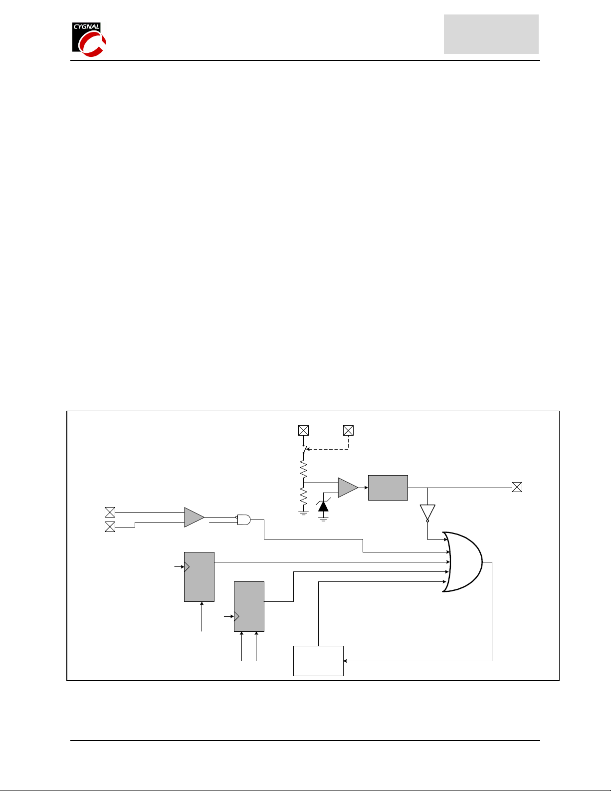
PRELIMINARY
C8051F206
C8051F220/1/6
12. RESET SOURCES
The reset circuitry of the MCU allows the controller to be easily placed in a predefined default condition. On entry
to this reset state, the CIP-51 halts program execution, forces the external port pins to a known state and initializes
the SFRs to their defined reset values. Interrupts and timers are disabled. On exit, the program counter (PC) is reset,
and program execution starts at location 0x0000.
All of the SFRs are reset to predefined values. The reset values of the SFR bits are defined in the SFR detailed
descriptions. The contents of internal data memory are not changed during a reset and any previously stored data is
preserved. However, since the stack pointer SFR is reset, the stack is effectively lost even though the data on the
stack are not altered.
The I/O port latches are reset to 0xFF (all logic ones), activating internal weak pull-ups which take the external I/O
pins to a high state. The external I/O pins do not go high immediately, but will go high within 4 system clock cycles
after entering the reset state. If the source of reset is from the VDD Monitor or writing a ‘1’ to the PORSF bit, the
/RST pin is driven low until the end of the VDD reset timeout.
On exit from the reset state, the MCU uses the internal oscillator running at 2MHz as the system clock by default.
Refer to Section 13 for information on selecting and configuring the system clock source. The Watchdog Timer is
enabled using its longest timeout interval. (Section 12.7 details the use of the Watchdog Timer.) Once the system
clock source is stable, program execution begins at location 0x0000.
There are six sources for putting the MCU into the reset state: power-on/power-fail (VDD monitor), external /RST
pin, software commanded, Comparator 0, Missing Clock Detector, and Watchdog Timer. Each reset source is
described below:
Figure 12.1. Reset Sources Diagram
CP0+
CP0-
System
Clock
Comparator 0
+
-
Missing
Clock
Detector
EN
MCD
Enable
C0RSEF
VDD
WDT
PRE
EN
WDT
WDT
Enable
Strobe
CIP-51
MonEn
Supply
Monitor
+
-
SWRSF
(Software Reset)
System Reset
Supply
Reset
Timeout
(wired-OR)
Reset
Funnel
/RST
Core
Page 81 CYGNAL Integrated Products, Inc. 2001 5.2001; Rev. 1.1
Page 82

PRELIMINARY
C8051F206
C8051F220/1/6
12.1. Power-on Reset
The CIP-51 incorporates a power supply monitor that holds the MCU in the reset state until VDD rises above the
V
level during power-up. (See Figure 12.2 for timing diagram, and refer to Table 12.1 for the Electrical
RST
Characteristics of the power supply monitor circuit.) The /RST pin is asserted (low) until the end of the 100msec
VDD Monitor timeout in order to allow the VDD supply to become stable. The VDD monitor is enabled by pulling
the MONEN pin high (available only on 48-pin packages). The VDD monitor may be disabled by pulling the
MONEN pin low.
On exit from a power-on reset, the PORSF flag (RSTSRC.1) is set by hardware to logic 1. All of the other reset
flags in the RSTSRC Register are indeterminate. PORSF is cleared by all other resets. Since all resets cause
program execution to begin at the same location (0x0000), software can read the PORSF flag to determine if a
power-up was the cause of reset. The content of internal data memory should be assumed to be undefined after a
power-on reset.
12.2. Software Forced Reset
Writing a 1 to the PORSF bit forces a Power-On Reset as described in Section 12.1.
Figure 12.2. VDD Monitor Timing Diagram
volts
2.70
2.55
2.0
1.0
Logic HIGH
Logic LOW
/RST
V
RST
D
D
V
t
100ms 100ms
12.3. Power-fail Reset
When the VDD monitor is enabled the MONEN pin (not on C8051F221/F231 32 pin parts) is “pulled high”,and
power-down transition or power irregularity causes VDD to drop below V
the /RST pin low and return the CIP-51 to the reset state (see Figure 12.2). When VDD returns to a level above
V
, the CIP-51 will leave the reset state in the same manner as that for the power-on reset. Note that even though
RST
internal data memory contents are not altered by the power-fail reset, it is impossible to determine if VDD dropped
below the level required for data retention. If the PORSF flag is set, the data may no longer be valid.
, the power supply monitor will drive
RST
Page 82 CYGNAL Integrated Products, Inc. 2001 5.2001; Rev. 1.1
Page 83

PRELIMINARY
C8051F206
C8051F220/1/6
12.4. External Reset
The external /RST pin provides a means for external circuitry to force the CIP-51 into a reset state. Asserting an
active-low signal on the /RST pin will cause the CIP-51 to enter the reset state. Although there is a weak pull-up, it
may be desirable to provide an external pull-up and/or decoupling of the /RST pin to avoid erroneous noise-induced
resets. The CIP-51 will remain in reset until at least 12 clock cycles after the active-low /RST signal is removed.
The PINRSF flag (RSTSRC.0) is set on exit from an external reset. The /RST pin is 5V tolerant.
12.5. Missing Clock Detector Reset
The Missing Clock Detector is essentially a one-shot circuit that is triggered by the MCU system clock. If the system
clock goes away for more than 100µsec, the one-shot will time out and generate a reset. After a Missing Clock
Detector reset, the MCDRSF flag (RSTSRC.2) will be set, signifying the MSD as the reset source; otherwise, this bit
reads 0. The state of the /RST pin is unaffected by this reset. Setting the MSCLKE bit in the OSCICN register (see
Figure 13.2) enables the Missing Clock Detector.
12.6. Comparator 0 Reset
Comparator 0 can be configured as a reset input by writing a 1 to the C0RSEF flag (RSTSRC.5). Comparator 0
should be enabled using CPT0CN.7 (see Figure 8.3) prior to writing to C0RSEF to prevent any turn-on chatter on
the output from generating an unwanted reset. When configured as a reset, if the non-inverting input voltage (on
CP0+) is less than the inverting input voltage (on CP0-), the MCU is put into the reset state. After a Comparator 0
Reset, the C0RSEF flag (RSTSRC.5) will read 1 signifying Comparator 0 as the reset source; otherwise, this bit
reads 0. The state of the /RST pin is unaffected by this reset.
12.7. Watchdog Timer Reset
The MCU includes a programmable Watchdog Timer (WDT) running off the system clock. The WDT will force the
MCU into the reset state when the watchdog timer overflows. To prevent the reset, the WDT must be restarted by
application software before the overflow occurs. If the system experiences a software/hardware malfunction
preventing the software from restarting the WDT, the WDT will overflow and cause a reset. This should prevent the
system from running out of control.
The WDT is automatically enabled and started with the default maximum time interval on exit from all resets. If
desired, the WDT can be disabled by system software or locked ‘on’ to prevent accidental disabling. Once locked,
the WDT cannot be disabled until the next system reset. The state of the /RST pin is unaffected by this reset.
Page 83 CYGNAL Integrated Products, Inc. 2001 5.2001; Rev. 1.1
Page 84

PRELIMINARY
C8051F206
C8051F220/1/6
12.7.1. Watchdog Usage
The WDT consists of a 21-bit timer running from the programmed system clock. The timer measures the period
between specific writes to its control register. If this period exceeds the programmed limit, a WDT reset is
generated. The WDT can be enabled and disabled as needed in software, or can be permanently enabled if desired.
Watchdog features are controlled via the Watchdog Timer Control Register (WDTCN) shown in Figure 12.3.
Enable/Reset WDT
The watchdog timer is both enabled and reset by writing 0xA5 to the WDTCN register. The user’s application
software should include periodic writes of 0xA5 to WDTCN as needed to prevent a watchdog timer overflow. The
WDT is enabled and reset as a result of any system reset.
Disable WDT
Writing 0xDE followed by 0xAD to the WDTCN register disables the WDT. The following code segment illustrates
disabling the WDT.
CLR EA ; disable all interrupts
MOV WDTCN,#0DEh ; disable watchdog timer
MOV WDTCN,#0ADh ;
SETB EA ; re-enable interrupts
The writes of 0xDE and 0xAD must occur within 4 clock cycles of each other, or the disable operation is ignored.
Interrupts should be disabled during this procedure to avoid delay between the two writes.
Disable WDT Lockout
Writing 0xFF to WDTCN locks out the disable feature. Once locked out, the disable operation is ignored until the
next system reset. Writing 0xFF does not enable or reset the watchdog timer. Applications always intending to use
the watchdog should write 0xFF to WDTCN in their initialization code.
Setting WDT Interval
WDTCN.[2:0] control the watchdog timeout interval. The interval is given by the following equation:
3+WDTCN[2:0]
4
xT
SYSCLK
,(whereT
is the system clock period).
SYSCLK
For a 2.0 MHz system clock, this provides an interval range of 32msec to 524msec. WDTCN.7 must be written as 0
when setting this interval. Reading WDTCN returns the programmed interval. WDTCN.[2:0] is 111b after a system
reset.
Figure 12.3. WDTCN: Watchdog Timer Control Register
R/W R/W R/W R/W R/W R/W R/W R/W Reset Value
xxxxx111
Bit7 Bit6 Bit5 Bit4 Bit3 Bit2 Bit1 Bit0
SFR Address:
0xFF
Bits7-0: WDT Control
Writing 0xA5 both enables and reloads the WDT.
Writing 0xDE followed within 4 clocks by 0xAD disables the WDT.
Writing 0xFF locks out the disable feature.
Bit4: Watchdog Status Bit (when Read)
Reading the WDTCN.[4] bit indicates the Watchdog Timer Status.
0: WDT is inactive
1: WDT is active
Bits2-0: Watchdog Timeout Interval Bits
The WDTCN.[2:0] bits set the Watchdog Timeout Interval. When writing these bits,
WDTCN.7 must be set to 0.
Page 84 CYGNAL Integrated Products, Inc. 2001 5.2001; Rev. 1.1
Page 85

PRELIMINARY
C8051F206
C8051F220/1/6
Figure 12.4. RSTSRC: Reset Source Register
R R/W R/W R R R/W R Reset Value
- C0RSEF SWRSEF WDTRSF MCDRSF PORSF PINRSF xxxxxxxx
Bit7 Bit6 Bit5 Bit4 Bit3 Bit2 Bit1 Bit0
(Note: Do not use read-modify-write operations on this register.)
Bit7: RESERVED.
Bit6: Not Used. Read only 0b.
Bit5: C0RSEF: Comparator 0 Reset Enable and Flag
Write
0: Comparator 0 is not a reset source
1: Comparator 0 is a reset source
Read
0: Source of prior reset was not from Comparator 0
1: Source of prior reset was from Comparator 0
Bit4: SWRSF: Software Reset Force and Flag
Write
0: No Effect
1: Forces an internal reset. /RST pin is not affected.
Read
0: Prior reset source was not from write to the SWRSF bit.
1: Prior reset source was from write to the SWRSF bit.
Bit3: WDTRSF: Watchdog Timer Reset Flag (Read only)
0: Source of prior reset was not from WDT timeout.
1: Source of prior reset was from WDT timeout.
Bit2: MCDRSF: Missing Clock Detector Flag (Read only)
0: Source of prior reset was not from Missing Clock Detector timeout.
1: Source of prior reset was from Missing Clock Detector timeout.
Bit1: PORSF: Power-On Reset Force and Flag
Write
0: No effect
1: Forces a Power-On Reset. /RST is driven low.
Read
0: Source of prior reset was not from POR.
1: Source of prior reset was from POR.
Bit0: PINRSF: HW Pin Reset Flag
0: Source of prior reset was not from /RST pin.
1: Source of prior reset was from /RST pin.
SFR Address:
0xEF
Page 85 CYGNAL Integrated Products, Inc. 2001 5.2001; Rev. 1.1
Page 86

PRELIMINARY
C8051F206
C8051F220/1/6
Table 12.1. VDD Monitor Electrical Characteristics
-40°Cto+85°C unless otherwise specified.
PARAMETER CONDITIONS MIN TYP MAX UNITS
/RST Output Low Voltage IOL= 8.5mA, VDD = 2.7 to 3.6V 0.6 V
/RST Input High Voltage 0.8 x
VDD
/RST Input Low Voltage 0.2 x
VDD
/RST Input Leakage Current /RST = 0.0V 50
VDD for /RST Output Valid 1.0 V
Reset Threshold (Vrst) 2.40 2.55 2.70 V
Reset Time Delay /RST rising edge after crossing reset
threshold
Missing Clock Detector
Timeout
Time from last system clock to reset
generation
80 100 120 ms
100 220 500
µA
µs
V
V
Page 86 CYGNAL Integrated Products, Inc. 2001 5.2001; Rev. 1.1
Page 87

PRELIMINARY
C8051F206
C8051F220/1/6
13. OSCILLATOR
The MCU includes an internal oscillator and an external oscillator drive circuit, either of which can generate the
system clock. The MCU boots from the internal oscillator after any reset. This internal oscillator can be
enabled/disabled and its frequency can be set using the Internal Oscillator Control Register (OSCICN) as shown in
Figure 13.2. The internal oscillator’s electrical specifications are given in Table 13.1.
Both oscillators are disabled when the /RST pin is held low. The MCU can run from the internal oscillator
permanently, or it can switch to the external oscillator if desired using CLKSL bit in the OSCICN Register. The
external oscillator requires an external resonator, crystal, capacitor, or RC network connected to the XTAL1/XTAL2
pins (see Figure 13.1). The oscillator circuit must be configured for one of these sources in the OSCXCN register.
An external CMOS clock can also provide the system clock by driving the XTAL1 pin. The XTAL1 and XTAL2
pins are NOT 5V tolerant.
Figure 13.1. Oscillator Diagram
OSCICN
opt. 4
opt. 3
XTAL1
XTAL2
opt. 2
VDD
IFCN1
CLKSL
EN
OSC
IOSCEN
IFCN0
SYSCLK
IFRDY
MSCLKE
Internal Clock
Generator
opt. 1
XTAL1XTAL1
XTAL1
Input
Circuit
XTAL2
XFCN2
XFCN1
XTLVLD
XOSCMD2
XOSCMD1
XOSCMD0
XFCN0
OSCXCN
Page 87 CYGNAL Integrated Products, Inc. 2001 5.2001; Rev. 1.1
Page 88

PRELIMINARY
C8051F206
C8051F220/1/6
Figure 13.2. OSCICN: Internal Oscillator Control Register
R/W R/W R/W R/W R/W R/W R/W R/W Reset Value
MSCLKE - - IFRDY CLKSL IOSCEN IFCN1 IFCN0 00000100
Bit7 Bit6 Bit5 Bit4 Bit3 Bit2 Bit1 Bit0
Bit7: MSCLKE: Missing Clock Enable Bit
0: Missing Clock Detector Disabled
1: Missing Clock Detector Enabled; triggers a reset if a missing clock is detected
Bits6-5: UNUSED. Read = 00b, Write = don’t care
Bit4: IFRDY: Internal Oscillator Frequency Ready Flag
0: Internal Oscillator Frequency not running at speed specified by the IFCN bits.
1: Internal Oscillator Frequency running at speed specified by the IFCN bits.
Bit3: CLKSL: System Clock Source Select Bit
0: Uses Internal Oscillator as System Clock.
1: Uses External Oscillator as System Clock.
Bit2: IOSCEN: Internal Oscillator Enable Bit
0: Internal Oscillator Disabled
1: Internal Oscillator Enabled
Bits1-0: IFCN1-0: Internal Oscillator Frequency Control Bits
00: Internal Oscillator typical frequency is 2MHz.
01: Internal Oscillator typical frequency is 4MHz.
10: Internal Oscillator typical frequency is 8MHz.
11: Internal Oscillator typical frequency is 16MHz.
SFR Address:
0xB2
Table 13.1. Internal Oscillator Electrical Characteristics
-40°Cto+85°C unless otherwise specified.
PARAMETER CONDITIONS MIN TYP MAX UNITS
Internal Oscillator
Frequency
Internal Oscillator Current
OSCICN.[1:0] = 00
OSCICN.[1:0] = 01
OSCICN.[1:0] = 10
OSCICN.[1:0] = 11
1.6
3.2
6.4
12.8
2
4
8
16
OSCICN.2 = 1 200
2.4
4.8
9.6
19.2
Consumption
Internal Oscillator
4
Temperature Stability
Internal Oscillator Power
6.4 %/V
Supply (VDD) Stability
MHz
µA
ppm/°C
Page 88 CYGNAL Integrated Products, Inc. 2001 5.2001; Rev. 1.1
Page 89

PRELIMINARY
C8051F206
C8051F220/1/6
Figure 13.3. OSCXCN: External Oscillator Control Register
R R/W R/W R/W R/W R/W R/W R/W Reset Value
XTLVLD
Bit7 Bit6 Bit5 Bit4 Bit3 Bit2 Bit1 Bit0
Bit7: XTLVLD: Crystal Oscillator Valid Flag
Bits6-4: XOSCMD2-0: External Oscillator Mode Bits
Bit3: RESERVED. Read = undefined, Write = don’t care
Bits2-0: XFCN2-0: External Oscillator Frequency Control Bits
XOSCMD2 XOSCMD1 XOSCMD0
- XFCN2 XFCN1 XFCN0 00110000
(Valid only when XOSCMD = 1xx.)
0: Crystal Oscillator is unused or not yet stable
1: Crystal Oscillator is running and stable
00x: Off. XTAL1 pin is grounded internally.
010: System Clock from External CMOS Clock on XTAL1 pin.
011: System Clock from External CMOS Clock on XTAL1 pin divided by 2.
10x: RC/C Oscillator Mode with divide by 2 stage.
110: Crystal Oscillator Mode
111: Crystal Oscillator Mode with divide by 2 stage.
000-111: see table below
SFR Address:
0xB1
XFCN Crystal (XOSCMD = 11x) RC (XOSCMD = 10x) C (XOSCMD = 10x)
000 Power Factor = 30 (103)
001 Power Factor = 90 (103)
010 Power Factor = 260 (103)
011 Power Factor = 740 (103)
100 Power Factor = 2.10 (106)
101 Power Factor = 5.80 (106)
110 Power Factor = 22.0 (106)
111 Power Factor = 65.0 (106)
f ≤ 25kHz
25kHz < f ≤ 50kHz
50kHz < f ≤ 100kHz
100kHz < f ≤ 200kHz
200kHz < f ≤ 400kHz
400kHz < f ≤ 800kHz
800kHz < f ≤ 1.6MHz
1.6MHz < f ≤ 3.2MHz
CRYSTAL MODE (Circuit from Figure 13.1, Option 1; XOSCMD = 11x)
Choose XFCN value to match the crystal frequency.
RC MODE (Circuit from Figure 13.1, Option 2; XOSCMD = 10x)
Choose oscillation frequency range where:
f = 1.23(10
3
)/(R*C),where
f = frequency of oscillation in MHz
C = capacitor value in pF
R = Pull-up resistor value in kΩ
CMODE(Circuit from Figure 13.1, Option 3; XOSCMD = 10x)
Choose K Factor (KF) for the oscillation frequency desired:
f = KF / (C * AV+),where
f = frequency of oscillation in MHz
C = capacitor value on XTAL1, XTAL2 pins in pF
AV+ = Analog Power Supply on MCU in volts
K Factor = 0.44
K Factor = 1.4
K Factor = 4.4
K Factor = 13
K Factor = 38
K Factor = 100
K Factor = 420
K Factor = 1400
Page 89 CYGNAL Integrated Products, Inc. 2001 5.2001; Rev. 1.1
Page 90

PRELIMINARY
C8051F206
C8051F220/1/6
13.1. External Crystal Example
If a crystal were used to generate the system clock for the MCU, the circuit would be as shown in Figure 13.1,
Option 1. For an ECS-110.5-20-4 crystal, the resonate frequency is 11.0592MHz, the intrinsic capacitance is 7pF,
and the ESR is 60Ω. The compensation capacitors should be 33pF each, and the PWB parasitic capacitance is
estimated to be 2pF. The appropriate External Oscillator Frequency Control value (XFCN) from the Crystal column
in the table in Figure 13.3 (OSCXCN Register) should be 111b.
When the crystal oscillator is enabled, a transient pulse may appear on XTAL2, the crystal driver output, that is
sufficient to cause the XTLVLD bit in OSCXCN to go to '1' before the crystal has actually started. Introducing a
blanking interval of 1ms between enabling the crystal oscillator and checking the XTLVLD bit will prevent a
premature switch to the external oscillator. The recommend procedure is:
1. Enable the external oscillator
2. Wait 1 ms
3. Poll for XTLVLD '0' ==> '1'
4. Switch to the external oscillator
Switching to the external oscillator before the crystal oscillator has stabilized could result in unpredictable behavior.
NOTE: Crystal oscillator circuits are quite sensitive to PCB layout. The crystal should be placed as close as possible
to the XTAL pins on the device, keeping the traces as short as possible and shielded with ground plane from any
other traces which could introduce noise or interference.
13.2. External RC Example
If an external RC network were used to generate the system clock for the MCU, the circuit would be as shown in
Figure 13.1, Option 2. The capacitor must be no greater than 100pF, but using a very small capacitor will increase
the frequency drift due to the PWB parasitic capacitance. To determine the required External Oscillator Frequency
Control value (XFCN) in the OSCXCN Register, first select the RC network value to produce the desired frequency
of oscillation. If the frequency desired is 100kHz, let R = 246kΩ and C = 50pF:
f = 1.23(10
XFCN ≥ log
XFCN ≥ log
3
)/RC = 1.23(103) / [246 * 50] = 0.1MHz = 100kHz
(f/25kHz)
2
(100kHz/25kHz) = log2(4)
2
XFCN ≥ 2, or code 010
13.3. External Capacitor Example
If an external capacitor were used to generate the system clock for the MCU, the circuit would be as shown in Figure
13.1, Option 3. The capacitor must be no greater than 100pF, but using a very small capacitor will increase the
frequency drift due to the PWB parasitic capacitance. To determine the required External Oscillator Frequency
Control value (XFCN) in the OSCXCN Register, select the capacitor to be used and find the frequency of oscillation
from the equations below. Assume VDD = 3.0V and C = 50pF:
f = KF / (C * VDD) = KF / (50 * 3)
f = KF / 150
If a frequency of roughly 90kHz is desired, select the K Factor from the table in Figure 13.3 as KF = 13:
f = 13 /150 = 0.087MHz, or 87kHz
Therefore, the XFCN value to use in this example is 011.
Page 90 CYGNAL Integrated Products, Inc. 2001 5.2001; Rev. 1.1
Page 91

PRELIMINARY
C8051F206
C8051F220/1/6
14. PORT INPUT/OUTPUT
Description
The C8051F221/231 have three I/O Ports: Port0, Port1, and Port2. The C8051F206, C8051F220/6 and
C8051F230/6 have four I/O Ports: Port0, Port1, Port2, and Port3. A wide array of digital resources can be assigned
to these ports by the simple configuration of the port’s corresponding multiplexer (MUX). Please see Figure 8.1.
Additionally, all external port pins are available as analog input.
14.1. Port I/O Initialization
Port I/O initialization is straightforward. Registers PRT0MX, PRT1MX and PRT2MX must be loaded with the
appropriate values to select the digital I/O functions required by the design. The output driver characteristics of the
I/O pins are defined using the Port Configuration Registers PRT0CF, PRT1CF, PRT2CF and PRT3CF. Each Port
Output driver can be configured as either Open Drain or Push-Pull. This is required even for the digital resources
selected in the PRTnMX registers, and is not automatic.
Any or all pins may be configured as digital I/O or as analog input. The default mode is digital I/O. The P0MODE,
P1MODE, P2MODE, and P3MODE special function registers are used to configure the port pins as digital or analog
as defined in this section.
The final step is initializing the individual resources selected using the appropriate setup registers. Initialization
procedures for the various digital resources may be found in the detailed explanation of each available function. The
reset state of each register is shown in the figures that describe each individual register.
NOTE: The input mode of pins configured for use with Timer 0, 1, or 2 must be manually configured.
1. The output mode of all ports pins must be configured regardless of whether the port pin is either standard
general-purpose I/O or controlled by a digital peripheral.
2. For all pins used as Timer inputs (P0.4/T0, P0.5/T1, P0.6/T2, and P0.7/T2EX), the output mode must be
“open-drain” (which is the reset state), and “1” must be written to the associated port pin to prevent possible
contention for the port pin that could result in an overcurrent condition. For example, to configure a
Timer0, set PRT0MX’s T0E Timer0 enable bit to ‘1’ to route Timer0 to Port Pin P0.4. Then place P0.4/T0
in open-drain configuration (which is set in PRT0CF by default), and write a ‘1’ to P0.4 to set its output
state to high impedance for use as a digital peripheral input (port pins also default to logic high state upon
reset). Lastly, ensure P0MODE.4 is ‘1’ for digital input mode. (All pins default to digital input mode upon
reset.)
Page 91 CYGNAL Integrated Products, Inc. 2001 5.2001; Rev. 1.1
Page 92

PRELIMINARY
Figure 14.1. Port I/O Functional Block Diagram
C8051F206
C8051F220/1/6
SYSCLK
T0,T1,
T2
Timers
UART
External
INT0 &
INT1
Comparators
0&1
SPI
ADC
PRTnMX
Registers
Port
0
MUX
Port
1
MUX
Port
2
MUX
A
M
U
X
PRTnCF &
PnMODE
registers
Port0 I/O Cell
Port1 I/O Cell
Port2 I/O Cell
Port3 I/O Cell
External
pins
P0.0/TX
P0.1/RX
P0.2/INT0
P0.3/INT1
P0.4/T0
P0.5/T1
P0.6/T2
P0.7/T2EX
P1.0/CP0+
P1.1/CP0P1.2/CP0
P1.3/CP1+
P1.4/CP1P1.5/CP1
P1.6/SYSCK
P1.7
Any port pin may be
configured via software as an
analog input to the ADC
P2.0/SCK
P2.1/MISO
P2.2/MOSI
P2.3/NSS
P2.4
P2.5
P2.6
P2.7
P3.0
P3.1
P3.2
P3.3
P3.4
P3.5
P3.6
P3.7
Figure 14.2. Port I/O Cell Block Diagram
To Comparator Input (on
port 1 only)
ADC
Analog Select
WEAK PUD
PUSH-PULL
VDD
/PORT-OUTENABLE
PORT-OUTPUT
DGND
Digital Input
Digital Enable
Page 92 CYGNAL Integrated Products, Inc. 2001 5.2001; Rev. 1.1
VDD
(WEAK)
PORT
PAD
Page 93

PRELIMINARY
C8051F206
C8051F220/1/6
Figure 14.3. PRT0MX: Port I/O MUX Register 0
R/W R/W R/W R/W R/W R/W R R/W Reset Value
T2EXE T2E T1E T0E INT1E INT0E
Bit7 Bit6 Bit5 Bit4 Bit3 Bit2 Bit1 Bit0
-
Bit7: T2EXE: T2EX Enable Bit
0: T2EX unavailable at Port pin.
1: T2EX routed to Port Pin.
Bit6: T2E: T2 Enable Bit
0: T2 unavailable at Port pin.
1: T2 routed to Port Pin.
Bit5: T1E: T1 Enable Bit
0: T1 unavailable at Port pin.
1: T1 routed to Port Pin.
Bit4: T0E: T0 Enable Bit
0: T0 unavailable at Port pin.
1: T0 routed to Port Pin.
Bit3: INT1E: /INT1 Enable Bit
0: /INT1 unavailable at Port pin.
1: /INT1 routed to port pin.
Bit2: INT0E: /INT0 Enable Bit
0: /INT0 unavailable at Port pin.
1: /INT0routedtoPortPin.
Bit1: UNUSED. Read = 0, Write = don’t care.
Bit0: UARTEN: UART I/O Enable
0: UART I/O unavailable at port pins.
1: TX, RX routed to pins P0.0 and P0.1, respectively.
UARTEN 00000000
SFR Address:
0xE1
Page 93 CYGNAL Integrated Products, Inc. 2001 5.2001; Rev. 1.1
Page 94

PRELIMINARY
C8051F206
C8051F220/1/6
Figure 14.4. PRT1MX: Port I/O MUX Register 1
RR/WRRRRR/WR/WResetValue
-SYSCKE----CP1OENCP0OEN00000000
Bit7 Bit6 Bit5 Bit4 Bit3 Bit2 Bit1 Bit0
Bit7: UNUSED. Read = 0.
Bit6: SYSCKE: SYSCLK Output Enable Bit
0: SYSCLK unavailable at the port pin.
1: SYSCLK output routed to pin P1.6
Bits 5-2: UNUSED. Read = 0000b, Write = don’t care.
Bit1: CP1OEN: Comparator 1 Output Enable bit.
0: CP1 unavailable at Port pin.
1: CP1routedtoPortPinP1.5.
Bit0: CP0OEN: Comparator 0 Output Enable Bit
0: CP0 unavailable at port pin.
1: CP0 routed to port pin P1.2.
SFR Address:
0xE2
Figure 14.5. PRT2MX: Port I/O MUX Register 2
R/W R/W R/W R/W R/W R/W R/W R/W Reset Value
GWPUD
Bit7 Bit6 Bit5 Bit4 Bit3 Bit2 Bit1 Bit0
P3WPUD P2WPUD P1WPUD P0WPUD - - SPI0OEN 00000000
SFR Address:
0xE3
Bit 7: GWPUD: Global Port I/O Weak Pull-up Disable Bit
0: Weak Pull-ups Enabled for all ports.
1: Weak Pull-ups Disabled (Bits 6-3 Don’t cares)
Bit 6: P3WPUD: Port 3 Weak Pull-up Disable Bit
0: Weak Pull-ups Enabled for port 3
1: Weak Pull-ups Disabled for port 3
Bit 5: P2WPUD: Port 2 Weak Pull-up Disable Bit
0: Weak Pull-ups Enabled for port 2.
1: Weak Pull-ups Disabled for port 2
Bit 4: P1WPUD: Port 1 Weak Pull-up Disable Bit
0: Weak Pull-ups Enabled for port 1
1: Weak Pull-ups Disabled for port 1
Bit 3: P0WPUD: Port 0 Weak Pull-up Disable Bit
0: Weak Pull-ups Enabled for port 0
1: Weak Pull-ups Enabled for port 0
Bits 2-1: UNUSED. Read = 00b, Write = don’t care.
Bit 0: SPI0OEN: SPI Bus I/O Enable Bit.
0: SPI I/O unavailable at port pins.
1: SCK, MISO, MOSI, NSS routed to pins P2.0, P2.1, P2.2, and P2.3 respectively.
Page 94 CYGNAL Integrated Products, Inc. 2001 5.2001; Rev. 1.1
Page 95

PRELIMINARY
C8051F206
C8051F220/1/6
14.2. General Purpose Port I/O
Each I/O port is accessed through a corresponding special function register (SFR) that is both byte addressable and
bit addressable. When writing to a port, the value written to the SFR is latched to maintain the output data value at
each pin. When reading, the logic levels of the port’s input pins are returned regardless of the PRTnMX settings
(i.e., even when the pin is assigned to another signal by the MUX, the Port Register can always still read its
corresponding Port I/O pin), provided its pin is configured for digital input mode. The exception to this is the
execution of the read-modify-write instructions. The read-modify-write instructions when operating on a port SFR
are the following: ANL, ORL, XRL, JBC, CPL, INC, DEC, DJNZ and MOV, CLR or SETB, when the destination is
an individual bit in a port SFR. For these instructions, the value of the register (not the pin) is read, modified, and
written back to the SFR.
Figure 14.6. P0: Port0 Register
R/W R/W R/W R/W R/W R/W R/W R/W Reset Value
P0.7 P0.6 P0.5 P0.4 P0.3 P0.2 P0.1 P0.0 11111111
Bit7 Bit6 Bit5 Bit4 Bit3 Bit2 Bit1 Bit0
(bit addressable)
Bits7-0: P0.[7:0]
(Write – Output appears on I/O pins per PRT0MX, PRT1MX, and PRT2MX Registers)
0: Logic Low Output.
1: Logic High Output (high impedance if corresponding PRT0CF.n bit = 0)
(Read – Regardless of PRT0MX, PRT1MX, and PRT2MX Register settings).
0: P0.n pin is logic low.
1: P0.n pin is logic high.
SFR Address:
0x80
Figure 14.7. PRT0CF: Port0 Configuration Register
R/W R/W R/W R/W R/W R/W R/W R/W Reset Value
00000000
Bit7 Bit6 Bit5 Bit4 Bit3 Bit2 Bit1 Bit0
SFR Address:
0xA4
Bits7-0: PRT0CF.[7:0]: Output Configuration Bits for P0.7-P0.0 (respectively)
0: Corresponding P0.n Output mode is Open-Drain.
1: Corresponding P0.n Output mode is Push-Pull.
Page 95 CYGNAL Integrated Products, Inc. 2001 5.2001; Rev. 1.1
Page 96

PRELIMINARY
p
C8051F206
C8051F220/1/6
Figure 14.8. P0MODE: Port0 Digital/Analog Input Mode
R/W R/W R/W R/W R/W R/W R/W R/W Reset Value
11111111
Bit7 Bit6 Bit5 Bit4 Bit3 Bit2 Bit1 Bit0
Bits7-0: Port0 Digital/Analog Input Mode
0: Corresponding Port0 pin Digital Input disabled. (For analog use, i.e., ADC or
comparators).
1: Corres
ondingPort0pin Digital Input is enabled.
Figure 14.9. P1: Port1 Register
R/W R/W R/W R/W R/W R/W R/W R/W Reset Value
P1.7 P1.6 P1.5 P1.4 P1.3 P1.2 P1.1 P1.0 11111111
Bit7 Bit6 Bit5 Bit4 Bit3 Bit2 Bit1 Bit0
(bit addressable)
SFR Address:
SFR Address:
0x90
0xF1
Bits7-0: P1.[7:0]
(Write – Output appears on I/O pins per PRT0MX, PRT1MX, and PRT2MX registers)
0: Logic Low Output.
1: Logic High Output (high impedance if corresponding PRT1CF.n bit = 0)
(Read – Regardless of PRT0MX, PRT1MX, and PRT2MX Register settings).
0: P1.n pin is logic low.
1: P1.n pin is logic high.
Figure 14.10. PRT1CF: Port1 Configuration Register
R/W R/W R/W R/W R/W R/W R/W R/W Reset Value
00000000
Bit7 Bit6 Bit5 Bit4 Bit3 Bit2 Bit1 Bit0
SFR Address:
0xA5
Bits7-0: PRT1CF.[7:0]: Output Configuration Bits for P1.7-P1.0 (respectively)
0: Corresponding P1.n Output Mode is Open-Drain.
1: Corresponding P1.n Output Mode is Push-Pull.
Page 96 CYGNAL Integrated Products, Inc. 2001 5.2001; Rev. 1.1
Page 97

PRELIMINARY
p
C8051F206
C8051F220/1/6
Figure 14.11. P1MODE: Port1 Digital/Analog Input Mode
R/W R/W R/W R/W R/W R/W R/W R/W Reset Value
11111111
Bit7 Bit6 Bit5 Bit4 Bit3 Bit2 Bit1 Bit0
Bits7-0: Port0 Digital/Analog Output Mode
0: Corresponding Port1 pin Digital Input disabled. (For analog use, i.e., ADC or
comparators).
1: Corres
ondingPort1pin Digital Input is enabled.
Figure 14.12. PRT1IF: Port1 Interrupt Flag Register
R/W R/W R/W R/W R/W R/W R/W R/W Reset Value
IE7 IE6 IE5 IE4 - - - - 00000000
Bit7 Bit6 Bit5 Bit4 Bit3 Bit2 Bit1 Bit0
SFR Address:
SFR Address:
0xAD
0xF2
Bit7: IE7: External Interrupt 7 Pending Flag.
0: No falling edge detected on P1.7.
1: This flag is set by hardware when a falling edge on P1.7 is detected.
Bit6: IE6: External Interrupt 6 Pending Flag.
0: No falling edge detected on P1.6.
1: This flag is set by hardware when a falling edge on P1.6 is detected.
Bit5: IE5: External Interrupt 5 Pending Flag.
0: No falling edge detected on P1.5.
1: This flag is set by hardware when a falling edge on P1.5 is detected.
Bit4: IE4: External Interrupt 4 Pending Flag.
0: No falling edge detected on P1.4.
1: This flag is set by hardware when a falling edge on P1.4 is detected.
Bits3-0: UNUSED. Read = 0000b, Write = don’t care.
Note: The Input Mode must be configured to Digital Mode in order for the falling edges to
be detected.
Page 97 CYGNAL Integrated Products, Inc. 2001 5.2001; Rev. 1.1
Page 98

PRELIMINARY
C8051F206
C8051F220/1/6
Figure 14.13. P2: Port2 Register
R/W R/W R/W R/W R/W R/W R/W R/W Reset Value
P2.7 P2.6 P2.5 P2.4 P2.3 P2.2 P2.1 P2.0 11111111
Bit7 Bit6 Bit Bit4 Bit3 Bit2 Bit1 Bit0
(bit addressable)
Bits7-0: P2.[7:0]
(Write – Output appears on I/O pins per PRT0MX, PRT1MX, and PRT2MX registers)
0: Logic Low Output.
1: Logic High Output (high impedance if corresponding PRT2CF.n bit = 0)
(Read – Regardless of PRT0MX, PRT1MX, and PRT2MX Register settings).
0: P2.n is logic low.
1: P2.n is logic high.
Figure 14.14. PRT2CF: Port2 Configuration Register
SFR Address:
0xA0
R/W R/W R/W R/W R/W R/W R/W R/W Reset Value
00000000
Bit7 Bit6 Bit5 Bit4 Bit3 Bit2 Bit1 Bit0
SFR Address:
0xA6
Bits7-0: PRT2CF.[7:0]: Output Configuration Bits for P2.7-P2.0 (respectively)
0: Corresponding P2.n Output Mode is Open-Drain.
1: Corresponding P2.n Output Mode is Push-Pull.
Figure 14.15. P2MODE: Port2 Digital/Analog Input Mode
R/W R/W R/W R/W R/W R/W R/W R/W Reset Value
11111111
Bit7 Bit6 Bit5 Bit4 Bit3 Bit2 Bit1 Bit0
SFR Address:
0xF3
Bits7-0: Port0 Digital/Analog Output Mode
0: Corresponding Port2 pin Digital Input disabled. (For analog use, i.e., ADC or
comparators).
1: Corresponding Port2 pin Digital Input is enabled.
Page 98 CYGNAL Integrated Products, Inc. 2001 5.2001; Rev. 1.1
Page 99

PRELIMINARY
C8051F206
C8051F220/1/6
Figure 14.16. P3: Port3 Register*
R/W R/W R/W R/W R/W R/W R/W R/W Reset Value
P3.7 P3.6 P3.5 P3.4 P3.3 P3.2 P3.1 P3.0 11111111
Bit7 Bit6 Bit5 Bit4 Bit3 Bit2 Bit1 Bit0
(bit addressable)
Bits7-0: P3.[7:0]
(Write)
0: Logic Low Output.
1: Logic High Output (high impedance if corresponding PRT3CF.n bit = 0)
(Read)
0: P3.n is logic low.
1: P3.n is logic high.
Figure 14.17. PRT3CF: Port3 Configuration Register*
R/W R/W R/W R/W R/W R/W R/W R/W Reset Value
Bit7 Bit6 Bit5 Bit4 Bit3 Bit2 Bit1 Bit0
SFR Address:
0xB0
00000000
SFR Address:
0xA7
Bits7-0: PRT3CF.[7:0]: Output Configuration Bits for P3.7-P3.0 (respectively)
0: Corresponding P3.n Output Mode is Open-Drain.
1: Corresponding P3.n Output Mode is Push-Pull.
Figure 14.18. P3MODE: Port3 Digital/Analog Input Mode*
R/W R/W R/W R/W R/W R/W R/W R/W Reset Value
Bit7 Bit6 Bit5 Bit4 Bit3 Bit2 Bit1 Bit0
Bits7-0: Port0 Digital/Analog Output Mode
0: Corresponding Port3 pin Digital Input disabled. (For analog use, i.e., ADC or
comparators).
1: Corresponding Port3 pin Digital Input is enabled.
11111111
SFR Address:
0xF4
* (Available on C8051F206, C8051F220/6 and C8051F230/6)
Page 99 CYGNAL Integrated Products, Inc. 2001 5.2001; Rev. 1.1
Page 100

PRELIMINARY
C8051F206
C8051F220/1/6
Table 14.1. Port I/O DC Electrical Characteristics
VDD = 2.7 to 3.6V, -40°Cto+85°C unless otherwise specified.
PARAMETER CONDITIONS MIN TYP MAX UNITS
Output High Voltage IOH= -10uA, Port I/O push-pull
VDD –
0.1
= -3mA, Port I/O push-pull
I
OH
VDD –
0.7
I
= -10mA, Port I/O push-pull
OH
VDD –
0.8
Output Low Voltage IOL= 10uA
I
=8.5mA
OL
I
= 25mA 1.0
OL
0.1
0.6
Input High Voltage 0.7 x
VDD
Input Low Voltage 0.3 x
VDD
Input Leakage Current DGND < Port Pin < VDD, Pin Tri-state
Weak Pull-up Off
±1
Weak Pull-up On 30
Capacitive Loading 3 pF
V
V
V
V
µA
Page 100 CYGNAL Integrated Products, Inc. 2001 5.2001; Rev. 1.1
 Loading...