

Page 1
DATA SHEET
SILICONDRIVE PC CARD
SSD-PXXX(I)-3521
OVERVIEW
The SiliconDrive PC Card is an optimal
time-to-market replacement for hard
drives and flash cards or in host systems
that require low power and scalable
storage solutions.
SiliconDrive technology is engineered
exclusively for the high performance, high
reliability, and multiyear product lifecycle
requirements of the Enterprise System
OEM market. Typical end-market
applications include broadband data and
voice networks, military systems, flight
system avionics, medical equipment,
industrial control systems, video
surveillance, storage networking, VoIP,
wireless infrastructure, and interactive
kiosks.
Every SiliconDrive is integrated with
SiliconSystems’ PowerArmor technology
to virtually eliminate storage systems
failures.
PowerArmor prevents data corruption and
loss from power disturbances by
integrating patented technology into every
SiliconDrive.
FEATURES
• RoHS 6 of 6 compliant
• Integrated PowerArmor technology
• Capacity range: 32MB to 8GB
• Supports both 8-bit and 16-bit data
register transfers
• Supports dual-voltage 3.3V or 5V
interface
• Data reliability <1 error in 1014 bits read
• MTBF 4,000,000 hours
• ATA-3 compliant
• Industry standard Type II PC Card form
factor
• Supports PIO modes 0-4
8GB
SSD-P08G(I)-3521
Numerous SiliconSystems’ patented and
patent-pending application-specific
technologies can be integrated into
SiliconDrive to safeguard application data
and software IP. Application notes
detailing these performance-enhancing
options are available under NDA.
Click here Click here
SILICONSYSTEMS PROPRIETARY
This document and the information contained within it is confidential and proprietary to SiliconSystems, Inc.
LISO VIEJO PARKWAY, ALISO VIEJO, CA 92656 • PHONE: 949.900.9400 • FAX: 949.900.9500 • http://www.siliconsystems.com
26840 A
3521P-02DSR FEBRUARY 2, 2009
All unauthorized use and/or reproduction is prohibited.
Page 2

REVISION HISTORY SSD-PXXX(I)-3521 DATA SHEET
REVISION HISTORY
Document No. Release Date Changes
3521P-02DSR February 2, 2009 Updated:
• "System Reliability" table and changed
the name to "Reliability."
• "Related Documentation" table.
Added:
• “Projected Operational Life Span.”
3521P-01DSR May 19, 2008 Updated “Overview.”
SSDS00-3521P-R March 12, 2008 Initial release.
SILICONSYSTEMS PROPRIETARY
This document and the information contained within it is confidential and proprietary to SiliconSystems, Inc.
3521P-02DSR PAGE II FEBRUARY 2, 2009
All unauthorized use and/or reproduction is prohibited.
Page 3

TABLE OF CONTENTS SSD-PXXX(I)-3521 DATA SHEET
TABLE OF CONTENTS
Overview..........................................................................................................................i
Features...........................................................................................................................i
Revision History..............................................................................................................II
List of Figures...............................................................................................................VII
List of Tables................................................................................................................ VIII
Physical Specifications.................................................................................................1
Physical Dimensions .................................................................................................... 1
Product Specifications..................................................................................................2
System Performance.................................................................................................... 2
System Power Requirements....................................................................................... 2
Reliability...................................................................................................................... 3
Projected Operational Life Span .................................................................................. 3
Product Capacity Specifications................................................................................... 4
Environmental Specifications ....................................................................................... 4
Electrical Specification..................................................................................................5
Pin Assignments........................................................................................................... 5
Signal Descriptions....................................................................................................... 7
Absolute Maximum Ratings........................................................................................ 15
Capacitance ............................................................................................................... 16
DC Characteristics ..................................................................................................... 16
AC Characteristics...................................................................................................... 17
Attribute and Common Memory Read Timing...................................................... 17
Attribute and Common Memory Write Timing ...................................................... 18
I/O Access Read Timing....................................................................................... 19
I/O Access Write Timing....................................................................................... 20
True IDE Read/Write Access Timing.................................................................... 21
True IDE Multiword DMA Read/Write Access Timing .......................................... 22
SILICONSYSTEMS PROPRIETARY
This document and the information contained within it is confidential and proprietary to SiliconSystems, Inc.
3521P-02DSR PAGE III FEBRUARY 2, 2009
All unauthorized use and/or reproduction is prohibited.
Page 4

TABLE OF CONTENTS SSD-PXXX(I)-3521 DATA SHEET
Attribute Memory Description and Operation...........................................................23
Attribute Memory Read Operations............................................................................ 23
Attribute Memory Write Operations............................................................................ 24
Attribute Memory Map................................................................................................ 25
Card Information Structure......................................................................................... 26
Configuration Option Register (200h)......................................................................... 37
Configuration and Status Register (202h).................................................................. 38
Pin Placement Register (204h) .................................................................................. 39
Socket and Copy Register (206h) .............................................................................. 40
Common Memory Description and Operation ..........................................................41
Common Memory Read Operations........................................................................... 41
Common Memory Write Operations........................................................................... 41
I/O Space Description and Operation ........................................................................42
I/O Space Read Operations ....................................................................................... 42
I/O Space Write Operations ....................................................................................... 42
ATA and True IDE Register Decoding........................................................................43
Memory-Mapped Register Decoding.......................................................................... 43
Independent I/O Mode Register Decoding ................................................................. 44
Primary and Secondary I/O Mapped Register Decoding ........................................... 45
Task File Register Specification................................................................................. 46
ATA Registers............................................................................................................... 47
Data Register ............................................................................................................. 47
Error Register............................................................................................................. 47
Feature Register......................................................................................................... 48
Sector Count Register................................................................................................ 49
Sector Number Register............................................................................................. 50
Cylinder Low Register ................................................................................................ 51
Cylinder High Register ............................................................................................... 52
Drive/Head Register................................................................................................... 53
SILICONSYSTEMS PROPRIETARY
This document and the information contained within it is confidential and proprietary to SiliconSystems, Inc.
3521P-02DSR PAGE IV FEBRUARY 2, 2009
All unauthorized use and/or reproduction is prohibited.
Page 5

TABLE OF CONTENTS SSD-PXXX(I)-3521 DATA SHEET
Status Register........................................................................................................... 54
Command Register .................................................................................................... 55
Alternate Status Register ........................................................................................... 56
Device Control Register ............................................................................................. 57
Device Address Register............................................................................................ 58
ATA Command Block and Set Description................................................................59
ATA Command Set .................................................................................................... 59
Check Power Mode — 98h, E5h .......................................................................... 61
Executive Drive Diagnostic — 90h....................................................................... 62
Format Track — 50h ............................................................................................ 63
Identify Drive — ECh............................................................................................ 64
Identify Drive — Drive Attribute Data............................................................. 65
Idle — 97h, E3h.................................................................................................... 68
Idle Immediate — 95h, E1h.................................................................................. 69
Initialize Drive Parameters — 91h........................................................................ 70
Recalibrate — 1Xh ............................................................................................... 71
Read Buffer — E4h .............................................................................................. 72
Read DMA — C8h................................................................................................ 73
Read Multiple — C4h ........................................................................................... 74
Read Sector — 20h, 21h...................................................................................... 75
Read Long Sector(s) — 22h, 23h......................................................................... 76
Read Verify Sector(s) — 40h, 41h ....................................................................... 77
Seek — 7Xh ......................................................................................................... 78
Set Features — EFh............................................................................................. 79
Set Multiple Mode — C6h .................................................................................... 80
Set Sleep Mode — 99h, E6h................................................................................ 81
Standby — 96h, E2h ............................................................................................ 82
Standby Immediate — 94h, E0h .......................................................................... 83
Write Buffer — E8h .............................................................................................. 84
SILICONSYSTEMS PROPRIETARY
This document and the information contained within it is confidential and proprietary to SiliconSystems, Inc.
3521P-02DSR PAGE V FEBRUARY 2, 2009
All unauthorized use and/or reproduction is prohibited.
Page 6

TABLE OF CONTENTS SSD-PXXX(I)-3521 DATA SHEET
Write DMA — CAh ............................................................................................... 85
Write Multiple — C5h ........................................................................................... 86
Write Sector(s) — 30h, 31h.................................................................................. 87
Write Long Sector(s) — 32h, 33h......................................................................... 88
Erase Sector(s) — C0h ........................................................................................ 89
Request Sense — 03h ......................................................................................... 90
Translate Sector — 87h ....................................................................................... 91
Wear-Level — F5h ............................................................................................... 92
Write Multiple w/o Erase — CDh.......................................................................... 93
Write Sector(s) w/o Erase — 38h......................................................................... 94
Write Verify — 3Ch............................................................................................... 95
Sales and Support .......................................................................................................96
Part Numbering............................................................................................................96
Nomenclature............................................................................................................. 96
Part Numbers ............................................................................................................. 97
RoHS 6 of 6 Product Labeling — Pb-Free Identification Label .................................. 97
Sample Label ............................................................................................................. 98
Related Documentation............................................................................................... 99
SILICONSYSTEMS PROPRIETARY
This document and the information contained within it is confidential and proprietary to SiliconSystems, Inc.
3521P-02DSR PAGE VI FEBRUARY 2, 2009
All unauthorized use and/or reproduction is prohibited.
Page 7

LIST OF FIGURES SSD-PXXX(I)-3521 DATA SHEET
LIST OF FIGURES
Figure 1: Physical Dimensions......................................................................................... 1
Figure 2: Attribute and Common Memory Read Timing Diagram.................................. 17
Figure 3: Attribute and Common Memory Write Timing Diagram .................................. 18
Figure 4: I/O Access Read Timing Diagram .................................................................. 19
Figure 5: I/O Access Write Timing Diagram................................................................... 20
Figure 6: True IDE Read/Write Access Timing Diagram ............................................... 21
Figure 7: True IDE Multiword DMA Read/Write Access Timing..................................... 22
Figure 8: Sample Label.................................................................................................. 98
SILICONSYSTEMS PROPRIETARY
This document and the information contained within it is confidential and proprietary to SiliconSystems, Inc.
3521P-02DSR PAGE VII FEBRUARY 2, 2009
All unauthorized use and/or reproduction is prohibited.
Page 8

LIST OF TABLES SSD-PXXX(I)-3521 DATA SHEET
LIST OF TABLES
Table 1: System Performance ......................................................................................... 2
Table 2: System Power Requirements ............................................................................ 2
Table 3: Reliability............................................................................................................3
Table 4: Operational Life Span ........................................................................................ 3
Table 5: Product Capacity Specifications ........................................................................ 4
Table 6: Environmental Specifications............................................................................. 4
Table 7: Pin Assignments ................................................................................................ 5
Table 8: Signal Descriptions ............................................................................................ 7
Table 9: Absolute Maximum Ratings ............................................................................. 15
Table 10: Capacitance................................................................................................... 16
Table 11: DC Characteristics ......................................................................................... 16
Table 12: Attribute and Common Memory Read Timing................................................ 17
Table 13: Attribute and Common Memory Write Timing................................................ 18
Table 14: I/O Access Read Timing ................................................................................ 19
Table 15: I/O Access Write Timing ................................................................................ 20
Table 16: True IDE Read/Write Access Timing ............................................................. 21
Table 17: True IDE Multiword DMA Read/Write Access Timing.................................... 22
Table 18: Attribute Memory Read Operations ............................................................... 23
Table 19: Attribute Memory Write Operations................................................................ 24
Table 20: Attribute Memory Map.................................................................................... 25
Table 21: Card Information Structure............................................................................. 26
Table 22: Configuration Option Register (200h) ............................................................ 37
Table 23: Configuration and Status Register (202h)...................................................... 38
Table 24: Pin Placement Register (204h)...................................................................... 39
Table 25: Socket and Copy Register (206h).................................................................. 40
Table 26: Common Memory Read Operations .............................................................. 41
Table 27: Common Memory Write Operations .............................................................. 41
SILICONSYSTEMS PROPRIETARY
This document and the information contained within it is confidential and proprietary to SiliconSystems, Inc.
3521P-02DSR PAGE VIII FEBRUARY 2, 2009
All unauthorized use and/or reproduction is prohibited.
Page 9

LIST OF TABLES SSD-PXXX(I)-3521 DATA SHEET
Table 28: I/O Space Read Operations........................................................................... 42
Table 29: I/O Space Write Operations........................................................................... 42
Table 30: Memory-Mapped Register Decoding ............................................................. 43
Table 31: Independent I/O Mode Register Decoding..................................................... 44
Table 32: Primary and Secondary I/O Mapped Register Decoding ............................... 45
Table 33: Task File Register Specification..................................................................... 46
Table 34: Error Register................................................................................................. 47
Table 35: Feature Register ............................................................................................ 48
Table 36: Sector Count Register.................................................................................... 49
Table 37: Sector Number Register ................................................................................ 50
Table 38: Cylinder Low Register.................................................................................... 51
Table 39: Cylinder High Register................................................................................... 52
Table 40: Drive/Head Register....................................................................................... 53
Table 41: Status Register .............................................................................................. 54
Table 42: Command Register ........................................................................................ 55
Table 43: Alternate Status Register............................................................................... 56
Table 44: Device Control Register ................................................................................. 57
Table 45: Device Address Register ............................................................................... 58
Table 46: ATA Command Block and Set Description .................................................... 59
Table 47: ATA Command Set ........................................................................................ 59
Table 48: Check Power Mode — 98h, E5h.................................................................... 61
Table 49: Executive Drive Diagnostic — 90h................................................................. 62
Table 50: Format Track — 50h...................................................................................... 63
Table 51: Identify Drive — ECh ..................................................................................... 64
Table 52: Identify Drive — Drive Attribute Data............................................................. 65
Table 53: Idle — 97h, E3h ............................................................................................. 68
Table 54: Idle Immediate — 95h, E1h ........................................................................... 69
Table 55: Initialize Drive Parameters — 91h ................................................................. 70
Table 56: Recalibrate — 1Xh......................................................................................... 71
SILICONSYSTEMS PROPRIETARY
This document and the information contained within it is confidential and proprietary to SiliconSystems, Inc.
3521P-02DSR PAGE IX FEBRUARY 2, 2009
All unauthorized use and/or reproduction is prohibited.
Page 10

LIST OF TABLES SSD-PXXX(I)-3521 DATA SHEET
Table 57: Read Buffer — E4h........................................................................................ 72
Table 58: Read DMA — C8h ......................................................................................... 73
Table 59: Read Multiple — C4h..................................................................................... 74
Table 60: Read Sector — 20h, 21h ............................................................................... 75
Table 61: Read Long Sector(s) — 22h, 23h .................................................................. 76
Table 62: Read Verify Sector(s) — 40h, 41h................................................................. 77
Table 63: Seek — 7Xh................................................................................................... 78
Table 64: Set Features — EFh ...................................................................................... 79
Table 65: Set Features’ Attributes ................................................................................. 79
Table 66: Set Multiple Mode — C6h .............................................................................. 80
Table 67: Set Sleep Mode — 99h, E6h ......................................................................... 81
Table 68: Standby — 96h, E2h...................................................................................... 82
Table 69: Standby Immediate — 94h, E0h.................................................................... 83
Table 70: Write Buffer — E8h ........................................................................................ 84
Table 71: Write DMA — CAh......................................................................................... 85
Table 72: Write Multiple — C5h..................................................................................... 86
Table 73: Write Sector(s) — 30h, 31h ........................................................................... 87
Table 74: Write Long Sector(s) — 32h, 33h .................................................................. 88
Table 75: Erase Sector(s) — C0h.................................................................................. 89
Table 76: Request Sense — 03h................................................................................... 90
Table 77: Extended Error Codes ................................................................................... 90
Table 78: Translate Sector — 87h ................................................................................. 91
Table 79: Wear-Level — F5h......................................................................................... 92
Table 80: Write Multiple w/o Erase — CDh ................................................................... 93
Table 81: Write Sector(s) w/o Erase — 38h .................................................................. 94
Table 82: Write Verify — 3Ch ........................................................................................ 95
Table 83: Part Numbering Nomenclature ...................................................................... 96
Table 84: Part Numbers................................................................................................. 97
Table 85: Related Documentation ................................................................................. 99
SILICONSYSTEMS PROPRIETARY
This document and the information contained within it is confidential and proprietary to SiliconSystems, Inc.
3521P-02DSR PAGE X FEBRUARY 2, 2009
All unauthorized use and/or reproduction is prohibited.
Page 11
PHYSICAL SPECIFICATIONS SSD-PXXX(I)-3521 DATA SHEET
PHYSICAL SPECIFICATIONS
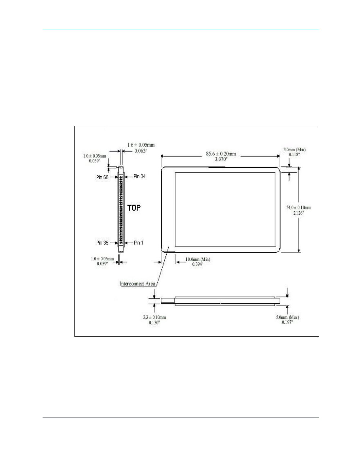
The SiliconDrive PC Card products are offered in a Type II form factor. See
"Part Numbering" on page 96 for details regarding PC Card capacities.
PHYSICAL DIMENSIONS
This section provides diagrams that describe the physical dimensions for the
PC Card.
Figure 1: Physical Dimensions
SILICONSYSTEMS PROPRIETARY
This document and the information contained within it is confidential and proprietary to SiliconSystems, Inc.
3521P-02DSR PAGE 1FEBRUARY 2, 2009
All unauthorized use and/or reproduction is prohibited.
Page 12

PRODUCT SPECIFICATIONS SSD-PXXX(I)-3521 DATA SHEET
PRODUCT SPECIFICATIONS
Note: All SiliconDrive PC Card values quoted are typical at 25°C and
nominal supply voltage.
SYSTEM PERFORMANCE
Table 1: System Performance
Reset to Ready Startup Time (Typical/Maximum) 200ms/400ms
Read Transfer Rate (Typical) 8MBps
Write Transfer Rate (Typical) 6MBps
Burst Transfer Rate 16.7MBps
Controller Overhead (Command to DRQ) 2ms (maximum)
SYSTEM POWER REQUIREMENTS
Table 2: System Power Requirements
DC Input Voltage 3.3 ± 10% 5.0 ± 10%
Sleep (Standby Current) <0.5mA <1.0mA
Read (Typical/Peak) 20mA/75mA 30mA/100mA
Write (Typical/Peak) 30mA/75mA 40mA/100mA
SILICONSYSTEMS PROPRIETARY
This document and the information contained within it is confidential and proprietary to SiliconSystems, Inc.
3521P-02DSR PAGE 2FEBRUARY 2, 2009
All unauthorized use and/or reproduction is prohibited.
Page 13

PRODUCT SPECIFICATIONS SSD-PXXX(I)-3521 DATA SHEET
RELIABILITY
Table 3: Reliability
MTBF (@ 25ºC) 4,000,000 hours
Bit Error Rate
<1 non-recoverable error in 10
14
bits read
PROJECTED OPERATIONAL LIFE SPAN
Table 4: Operational Life Span
SiliconDrive Part# Capacity Service Life* GB Written per Day
SSD-P08G-3521 8GB 324.3 Years @ 135.2GB
SSD-P04G-3521 4GB 162.2 Years @ 135.2GB
SSD-P02G-3521 2GB 81.1 Years @ 135.2GB
SSD-P01G-3521 1GB 40.5 Years @ 135.2GB
SSD-P51M-3521 512MB 20.3 Years @ 135.2GB
SSD-P25M-3521 256MB 10.1 Years @ 135.2GB
SSD-P12M-3521 128MB 5.1 Years @ 135.2GB
SSD-P64M-3521 64MB 2.5 Years @ 135.2GB
SSD-P32M-3521 32MB 1.3 Years @ 135.2GB
* There are unlimited read cycles. Service life is determined using
SiliconSystems’ LifeEst calculation at 100% duty cycle with 25% write cycles.
LifeEst is a comprehensive measurement that considers numerous factors to
determine the projected life span of a SiliconDrive. A white paper that
describes the benefits of LifeEst and how to calculate it can be found at http://
www.siliconsystems.com/resources/Documents/Whitepaper/
SiliconSystems_NAND_Evolution.pdf.
The actual life of a SiliconDrive is dependant on the customer usage model.
SiSMART is a patented technology of SiliconSystems that enables host
systems to monitor actual usage of a SiliconDrive in real time. SiSMART
measures and reports the remaining life of a SiliconDrive. For more
information on SiSMART, refer to the Eliminating Unsche duled Downtime by
Forecasting Useable Life white paper at http://www.siliconsystems.com/
technology/pdfs/SiliconDrive_SiSMART.pdf.
SILICONSYSTEMS PROPRIETARY
This document and the information contained within it is confidential and proprietary to SiliconSystems, Inc.
3521P-02DSR PAGE 3FEBRUARY 2, 2009
All unauthorized use and/or reproduction is prohibited.
Page 14

PRODUCT SPECIFICATIONS SSD-PXXX(I)-3521 DATA SHEET
PRODUCT CAPACITY SPECIFICATIONS
Table 5: Product Capacity Specifications
Product
Capacity
Capacity
(Bytes)
Number of
Sectors
32MB 32,702,464 63,872 499 4 32
64MB 65,601,536 128,128 1001 4 32
128MB 130,154,496 254,208 993 8 32
256MB 260,571,136 508,928 994 16 32
512MB 521,773,056 1,019,088 1011 16 63
1GB 1,047,674,880 2,046,240 2030 16 63
2GB 2,098,446,336 4,098,528 4066 16 63
4GB 4,224,761,856 8,251,488 8186 16 63
8GB 8,455,200,768 16,514,064 16,383* 16 63
* = All IDE drives 8GB and larger use 16383 cylinders, 16 heads, and 63 sectors/track due to
interface restrictions.
ENVIRONMENTAL SPECIFICATIONS
Table 6: Environmental Specifications
Number of
Cylinders
Number
of Heads
Number of
Sectors/
Track
Temperature 0ºC to 70ºC (Commercial)
-40ºC to 85ºC (Industrial)
Humidity 8% to 95% non-condensing
Vibration 16.3gRMS, MIL-STD-810F, Method 514.5, Procedure I,
Category 24
Shock 1000G, Half-sine, 0.5ms Duration
50g Pk, MIL-STD-810F, Method 516.5, Procedure I
Altitude 80,000ft, MIL-STD-810F, Method 500.4, Procedure II
SILICONSYSTEMS PROPRIETARY
This document and the information contained within it is confidential and proprietary to SiliconSystems, Inc.
All unauthorized use and/or reproduction is prohibited.
3521P-02DSR PAGE 4FEBRUARY 2, 2009
Page 15

ELECTRICAL SPECIFICATION SSD-PXXX(I)-3521 DATA SHEET
ELECTRICAL SPECIFICATION
PIN ASSIGNMENTS
The following table describes the SiliconDrive PC Card 50-pin IDE connector
signals.
Table 7: Pin Assignments
Pin
PC Card
Memory
Mode
PC Card
I/O Mode
IDE-ATA
Mode
Pin
PC Card
Memory
Mode
PC Card
I/O Mode
IDE-ATA
Mode
1 GND GND GND 35 GND GND GND
2 D3 D3 D3 36 CD1# CD1# CD1#
3D4 D4 D4 37
4D5 D5 D5 38
5D6 D6 D6 39
6D7 D7 D7 40
7 CE1# CE1# CS0# 41
8A10 A10
9OE# OE#
A10
OE#
2
2
42 CE2# CE2# CS1#
43 VS1# VS1# VS1#
D11
D12
D13
D14
D15
1
1
1
1
1
D11
D12
D13
D14
D15
1
1
1
1
1
D11
D12
D13
D14
D15
1
1
1
1
1
10 NU NU NU 44 IORD# IORD# IORD#
11 A9 A9
12 A8 A8
A9
A8
2
2
45 IOWR# IOWR# IOWR#
46 NU NU NU
13 NU NU NU 47 NU NU NU
14 NU NU NU 48 NU NU NU
15 WE# WE#
WE#
3
49 NU NU NU
16 RDY/BSY# IREQ INTRQ 50 NU NU NU
17 V
CC
V
CC
V
CC
51 V
CC
V
CC
V
CC
18 NU NU NU 52 NU NU NU
19 NU NU NU 53 NU NU NU
20 NU NU NU 54 NU NU NU
21 NU NU NU 55 NU NU NU
22 A7 A7
23 A6 A6
24 A5 A5
25 A4 A4
26 A3 A3
A7
A6
A5
A4
A3
2
2
2
2
2
56 NU NU CSEL#
57 VS2# VS2# VS2#
58 RESET RESET RESET#
59 WAIT# WAIT# IORDY
60 INPACK# INPACK# DMARQ
27 A2 A2 A2 61 REG# REG# DMACK#
SILICONSYSTEMS PROPRIETARY
This document and the information contained within it is confidential and proprietary to SiliconSystems, Inc.
3521P-02DSR PAGE 5FEBRUARY 2, 2009
All unauthorized use and/or reproduction is prohibited.
Page 16

ELECTRICAL SPECIFICATION SSD-PXXX(I)-3521 DATA SHEET
Pin
PC Card
Memory
Mode
PC Card
I/O Mode
IDE-ATA
Mode
28 A1 A1 A1 62
Pin
PC Card
Memory
Mode
3
BVD2
PC Card
I/O Mode
SPKR#
3
IDE-ATA
Mode
DASP#
29 A0 A0 A0 63 BVD1 STSCHG# PDIAG#
30 D0 D0 D0 64
31 D1 D1 D1 65
32 D2 D2 D2 66
D8
D9
D10
1
1
1
D8
D9
D10
1
1
1
D8
D9
D10
1
1
1
33 WP IOIS16# IOCS16# 67 CD2# CD2# CD2#
34 GND GND GND 68 GND GND GND
Notes:
NU = Not used
1 = These signals are required only for 16-bit access, and not required when installed in
8-bit systems.
2 = Should be grounded by the host.
SILICONSYSTEMS PROPRIETARY
This document and the information contained within it is confidential and proprietary to SiliconSystems, Inc.
3521P-02DSR PAGE 6FEBRUARY 2, 2009
All unauthorized use and/or reproduction is prohibited.
Page 17

ELECTRICAL SPECIFICATION SSD-PXXX(I)-3521 DATA SHEET
SIGNAL DESCRIPTIONS
Table 8: Signal Descriptions
Signal Name Pin Type Description
A10-A0 8, 10, 11,
12, 14, 15,
16, 17, 18,
19, 20
A10-A0
(PC Card I/O
mode)
A2-A0
18, 19, 20 I In true IDE mode, only A[2:0] are used
(True IDE mode)
BVD1
46 I/O This signal is asserted high, because
(PC Card memory
mode)
I These address lines along with the
-REG signal are used to select the
following:
• The I/O port address registers
within the SiliconDrive CF
• The memory-mapped port address
registers within the SiliconDrive CF
• A byte in the card's information
structure and its configuration
control and status registers
This signal is the same as the PC
Card Memory Mode signal.
to select the one of eight registers in
the Task File. The remaining address
lines should be grounded by the host.
BVD1 is not supported.
-STSCHG
(PC Card I/O
mode)
This signal is asserted low to alert the
host to changes in the RDY/-BSY and
Write Protect states while the I/O
interface is configured. This signal’s
use is controlled by the Card
Configuration and Status register.
-PDIAG
(True IDE mode)
In the true IDE mode, this input/output
is the Pass Diagnostic signal in the
Master/Slave handshake protocol.
BVD2
(PC Card memory
45 I/O This signal is asserted high, as BVD2
is not supported.
mode)
SILICONSYSTEMS PROPRIETARY
This document and the information contained within it is confidential and proprietary to SiliconSystems, Inc.
3521P-02DSR PAGE 7FEBRUARY 2, 2009
All unauthorized use and/or reproduction is prohibited.
Page 18

ELECTRICAL SPECIFICATION SSD-PXXX(I)-3521 DATA SHEET
Table 8: Signal Descriptions (Continued)
Signal Name Pin Type Description
-SPKR
(PC Card I/O
mode)
-DASP
(True IDE mode)
-CD1, -CD2
(PC Card memory
mode)
-CD1, -CD2
(PC Card I/O
Mode)
-CD1, -CD2
(True IDE mode)
-CE1, -CE2
(PC Card memory
mode)
Card Enable
This line is the Binary Audio output
from the card. If the Card does not
support the Binary Audio function, this
line should be held negated.
In the true IDE mode, this input/output
is the Disk Active/Slave Present
signal in the Master/Slave handshake
protocol.
26, 25 O These Card Detect pins are
connected to ground on the
SiliconDrive CF, and are used by the
host to determine that the SiliconDrive
CF is fully inserted into its socket.
This signal is the same for all modes.
This signal is the same for all modes.
7, 32 I These input signals are used both to
select the card and to indicate to the
card whether a byte or a word
operation is being performed.
• -CE2 always accesses the odd
byte of the word.
• -CE1 accesses the even byte or
the odd byte of the word depending
on A0 and -CE2.
A multiplexing scheme based on A0,
-CE1, and -CE2 allows 8-bit hosts to
access all data on D0-D7. See
"Attribute Memory Read Operations"
on page 23, "Attribute Memory Write
Operations" on page 24, "Common
Memory Read Operations" on page
41, and "Common Memory Write
Operations" on page 41.
SILICONSYSTEMS PROPRIETARY
This document and the information contained within it is confidential and proprietary to SiliconSystems, Inc.
3521P-02DSR PAGE 8FEBRUARY 2, 2009
All unauthorized use and/or reproduction is prohibited.
Page 19

ELECTRICAL SPECIFICATION SSD-PXXX(I)-3521 DATA SHEET
Table 8: Signal Descriptions (Continued)
Signal Name Pin Type Description
-CE1, -CE2
(PC Card I/O
mode)
Card Enable
-CS0, -CS1
(True IDE mode)
-CSEL
(PC Card memory
mode)
-CSEL
(PC Card I/O
mode)
-CSEL
(True IDE mode)
This signal is the same as the PC
Card Memory Mode signal. See "I/O
Space Read Operations" on page 42
and "I/O Space Write Operations" on
page 42.
In the true IDE mode, -CS0 is the chip
select for the task file registers while
-CS1 is used to select the Alternate
Status register and the Device Control
register.
39 I This signal is not used for this mode.
This signal is not used for this mode.
This internally pulled-up signal is used
to configure this device as a master or
slave when configured in the true IDE
mode.
When this pin is:
• Grounded, this device is configured
as a master.
• Open, this device is configured as
a slave.
-INPACK
43 O This signal is not used in this mode.
(PC Card memory
mode)
-INPACK
(PC Card I/O
mode)
Input Acknowledge
This signal is asserted by the
SiliconDrive CF when the card is
selected and responding to an I/O
read cycle at the address that is on
the address bus. This signal is used
by the host to control the enabling of
any input data buffers between the
SiliconDrive CF and the CPU.
SILICONSYSTEMS PROPRIETARY
This document and the information contained within it is confidential and proprietary to SiliconSystems, Inc.
All unauthorized use and/or reproduction is prohibited.
3521P-02DSR PAGE 9FEBRUARY 2, 2009
Page 20

ELECTRICAL SPECIFICATION SSD-PXXX(I)-3521 DATA SHEET
Table 8: Signal Descriptions (Continued)
Signal Name Pin Type Description
DMARQ
(True IDE mode)
D15-D00
(PC Card memory
mode)
43 O In true IDE mode, this signal is used
for DMA transfers between the host
and device. DMARQ is asserted by
the device when the device is ready to
transfer data to/from the host. The
direction of data transfer is controlled
by -IORD and -IOWR. This signal is
used in a handshake manner with
-DMACK (i.e., the device waits until
the host asserts -DMACK before
negating DMARQ, and reasserts
DMARQ if there is more data to
transfer). The DMARQ/-DMACK
handshake is used to provide flow
control during the transfer.
31, 30, 29,
28, 27, 49,
48, 47, 6,
5, 4, 3, 2,
23, 22, 21
I/O These lines carry the data,
commands, and status information
between the host and the controller.
• D00 is the LSB of the word’s even
byte.
• D08 is the LSB of the word’s odd
byte.
D15-D00
(PC Card I/O
This signal is the same as the PC
Card Memory Mode signal.
mode)
D15-D00
(True IDE mode)
In true IDE mode, all Task File
operations occur in byte mode on the
low-order bus D00-D07, while all data
transfers are 16 bits using D00-D15.
GND
1, 50 - Ground.
(PC Card memory
mode)
GND
This signal is the same for all modes.
(PC Card I/O
mode)
GND
This signal is the same for all modes.
(True IDE mode)
SILICONSYSTEMS PROPRIETARY
This document and the information contained within it is confidential and proprietary to SiliconSystems, Inc.
All unauthorized use and/or reproduction is prohibited.
3521P-02DSR PAGE 10 FEBRUARY 2, 2009
Page 21

ELECTRICAL SPECIFICATION SSD-PXXX(I)-3521 DATA SHEET
Table 8: Signal Descriptions (Continued)
Signal Name Pin Type Description
-IORD
(PC Card memory
mode)
-IORD
(PC Card I/O
mode)
-IORD
(True IDE mode)
-IOWR
(PC Card memory
mode)
-IOWR
(PC Card I/O
mode)
34 I This signal is not used in this mode.
This is an I/O read strobe generated
by the host. This signal gates I/O data
onto the bus from the SiliconDrive CF
when the card is configured to use the
I/O interface.
In true IDE mode, this signal has the
same function as the PC Card I/O
mode.
35 I This signal is not used in this mode.
The I/O write strobe pulse is used to
clock I/O data on the Card data bus
into the SiliconDrive CF controller
registers when the SiliconDrive CF is
configured to use the I/O interface.
-IOWR
(True IDE mode)
-OE
(PC Card memory
mode)
-OE
(PC Card I/O
mode)
The clocking occurs on the negativeto-positive edge of the signal (the
trailing edge).
In true IDE mode, this signal has the
same function as the PC Card I/O
mode.
9 I This is an output enable strobe
generated by the host interface, which
is used to read:
• Data from the SiliconDrive CF in
memory mode.
• The CIS and configuration
registers.
In PC Card I/O mode, this signal is
used to read the CIS and
configuration registers.
SILICONSYSTEMS PROPRIETARY
This document and the information contained within it is confidential and proprietary to SiliconSystems, Inc.
3521P-02DSR PAGE 11 FEBRUARY 2, 2009
All unauthorized use and/or reproduction is prohibited.
Page 22

ELECTRICAL SPECIFICATION SSD-PXXX(I)-3521 DATA SHEET
Table 8: Signal Descriptions (Continued)
Signal Name Pin Type Description
-ATA SEL
(True IDE mode)
-RDY/-BSY
(PC Card memory
mode)
To enable true IDE mode, this input
should be grounded by the host.
37 O In memory mode, this signal is:
• Set high when the SiliconDrive CF
is ready to accept a new data
transfer operation.
• Held low when the card is busy.
The host memory card socket must
provide a pull-up resistor.
At power-up and reset, the RDY/-BSY
signal is held low (busy) until the
SiliconDrive CF has completed its
power-up or reset function. No access
of any type should be made to the
SiliconDrive CF during this time. The
RDY/-BSY signal is held high
(disabled from being busy) whenever
the SiliconDrive CF has been
powered up with +RESET
continuously disconnected or
asserted.
-IREQ
(PC Card I/O
mode)
Input Acknowledge
I/O Operation. After the SiliconDrive
CF has been configured for I/O
operation, this signal is used as
-Interrupt Request. This line is strobed
low to generate a pulse mode
interrupt or held low for a level mode
interrupt.
-IREQ
(True IDE mode)
In true IDE mode, this signal is the
active high Interrupt Request to the
host.
SILICONSYSTEMS PROPRIETARY
This document and the information contained within it is confidential and proprietary to SiliconSystems, Inc.
All unauthorized use and/or reproduction is prohibited.
3521P-02DSR PAGE 12 FEBRUARY 2, 2009
Page 23

ELECTRICAL SPECIFICATION SSD-PXXX(I)-3521 DATA SHEET
Table 8: Signal Descriptions (Continued)
Signal Name Pin Type Description
-REG
(PC Card memory
mode)
Attribute Memory
Select
-REG
(PC Card I/O
mode)
-DMACK
(True IDE mode)
-RESET
(PC Card memory
mode)
44 I This signal is used during memory
cycles to distinguish between
common memory and register
(attribute) memory accesses. This
signal is set:
• High for common memory.
• Low for attribute memory.
The signal must also be active (low)
during I/O cycles when the I/O
address is on the bus.
In true IDE mode, this signal is used
by the host in response to DMARQ to
initiate DMA transfers. The DMARQ/
-DMACK handshake is used to
provide flow control during the
transfer. When -DMACK is asserted,
-CS0 and -CS1 are not asserted and
transfers are 16-bits wide.
41 I When the pin is high, this signal
resets the SiliconDrive CF. The
SiliconDrive CF is reset only at powerup if this pin is left high or open from
power-up. The SiliconDrive CF is also
reset when the Soft Reset bit in the
Card Configuration Option register is
set.
-RESET
(PC Card I/O
This signal is the same as the PC
Card Memory Mode signal.
mode)
-RESET
(True IDE mode)
In the true IDE mode, this input pin is
the active low hardware reset from the
host.
V
CC
13, 38 - +5V, +3.3V power.
(PC Card memory
mode)
SILICONSYSTEMS PROPRIETARY
This document and the information contained within it is confidential and proprietary to SiliconSystems, Inc.
3521P-02DSR PAGE 13 FEBRUARY 2, 2009
All unauthorized use and/or reproduction is prohibited.
Page 24

ELECTRICAL SPECIFICATION SSD-PXXX(I)-3521 DATA SHEET
Table 8: Signal Descriptions (Continued)
Signal Name Pin Type Description
V
CC
This signal is the same for all modes.
(PC Card I/O
mode)
V
CC
This signal is the same for all modes.
(True IDE mode)
-VS1, -VS2 33, 40 O V oltage Sense Signals.
• -VS1 is grounded so that the
SiliconDrive CF CIS can be read at
3.3V.
• -VS2 is reserved by PC Card for a
secondary voltage.
-VS1, -VS2
This signal is the same for all modes.
(PC Card I/O
mode)
-VS1, -VS2
This signal is the same for all modes.
(True IDE mode)
-WAIT
(PC Card memory
mode)
42 O The -WAIT signal is driven low by the
SiliconDrive CF to signal the host to
delay completion of a memory or I/O
cycle that is in progress.
-WAIT
(PC Card I/O
This signal is the same as the PC
Card Memory Mode signal.
mode)
-IORDY
(True IDE mode)
-WE
(PC Card memory
mode)
36 I This is a signal driven by the host and
In true IDE mode, this output signal
may be used as IORDY.
used for strobing memory write data
to the registers of the SiliconDrive CF
when the card is configured in the
memory interface mode. This signal is
also used for writing the configuration
registers.
-WE
(PC Card I/O
mode)
In PC Card I/O mode, this signal is
used for writing the configuration
registers.
SILICONSYSTEMS PROPRIETARY
This document and the information contained within it is confidential and proprietary to SiliconSystems, Inc.
All unauthorized use and/or reproduction is prohibited.
3521P-02DSR PAGE 14 FEBRUARY 2, 2009
Page 25

ELECTRICAL SPECIFICATION SSD-PXXX(I)-3521 DATA SHEET
Table 8: Signal Descriptions (Continued)
Signal Name Pin Type Description
-WE
(True IDE mode)
WP
(PC Card memory
mode)
-IOIS16
(PC Card I/O
mode)
-IOIS16
(True IDE mode)
In true IDE mode, this input signal is
not used and should be connected to
VCC by the host.
24 O Write Protect Memory Mode. The
SiliconDrive CF does not have a write
protect switch. This signal is held low
after the completion of the reset
initialization sequence.
I/O Operation. When the SiliconDrive
CF is configured for I/O operation, pin
24 is used for the -I/O Selected, which
is a 16-bit port (-IOIS16) function. A
low signal indicates that a 16-bit or
odd byte only operation can be
performed at the addressed port.
In true IDE mode, this output signal is
asserted low when this device is
expecting a word data transfer cycle.
ABSOLUTE MAXIMUM RATINGS
Table 9: Absolute Maximum Ratings
Symbol Parameter Minimum Maximum Units
T
T
V
V
V
s
A
CC
in
out
Storage Temperature -55 125 °C
Operating Temperature -40 85 °C
VCC with Respect to GND -0.3 6.7 V
Input Voltage -0.5 3.8 V
Output Voltage -0.3 3.6 V
SILICONSYSTEMS PROPRIETARY
This document and the information contained within it is confidential and proprietary to SiliconSystems, Inc.
3521P-02DSR PAGE 15 FEBRUARY 2, 2009
All unauthorized use and/or reproduction is prohibited.
Page 26
ELECTRICAL SPECIFICATION SSD-PXXX(I)-3521 DATA SHEET
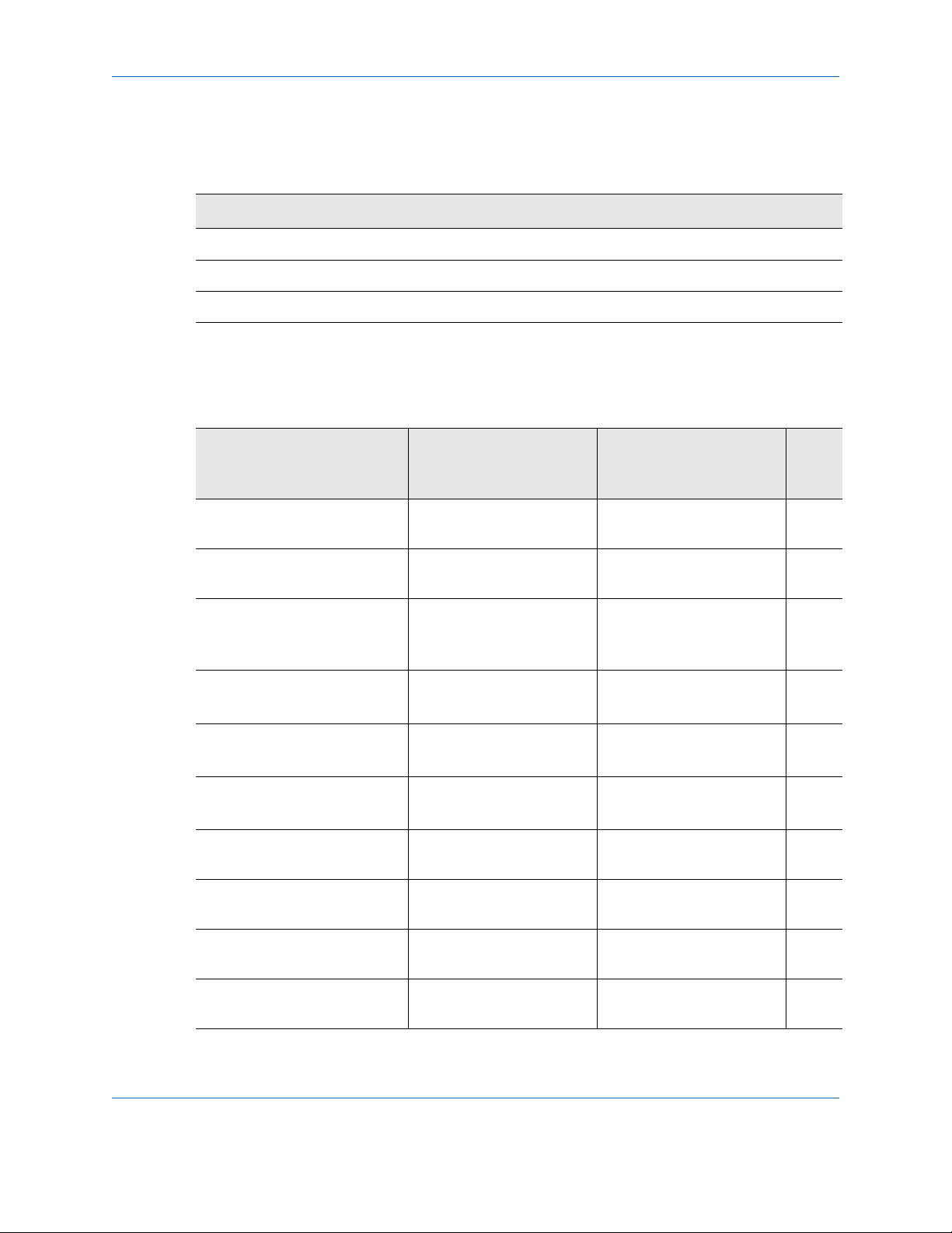
CAPACITANCE
Table 10: Capacitance
Symbol Parameter Maximum Units
C
in
C
out
C
I/O
DC CHARACTERISTICS
Symbol Parameter
V
I
I
V
LI
LO
CC
CCR
Power Supply
Voltage
Input Leakage
*(1) Current
Output
Leakage *(1)
Current
VCC Read
Current
Input Capacitance
Output Capacitance
Bidirectional Capacitance
Table 11: DC Characteristics
3.3 V ±10% 5V ±10%
Minimum Maximum Minimum Maximum
3.0 3.6 4.5 5.5 V
-5-5μA
-5-5μA
-50-80mA
35 pF
35 pF
35 pF
Units
V
CCW
VCC Write
-50-80mA
Current
V
CCS
VCC Standby
-0.3-0.5mA
Current
V
IL
Input Low
-0.3 0.3 x V
-0.3 0.3 x V
CC
CC
V
Voltage
V
IH
Input High
.7 x V
VCC + 0.3 .7 x V
CC
VCC + 0.3 V
CC
Voltage
V
OL
Output Low
-0.4-0.4V
Voltage
V
OH
Output High
VCC - 0.4 - VCC - 0.4 - V
Voltage
*(1) Except the pulled-up/pulled-down pin.
SILICONSYSTEMS PROPRIETARY
This document and the information contained within it is confidential and proprietary to SiliconSystems, Inc.
3521P-02DSR PAGE 16 FEBRUARY 2, 2009
All unauthorized use and/or reproduction is prohibited.
Page 27
ELECTRICAL SPECIFICATION SSD-PXXX(I)-3521 DATA SHEET
AC CHARACTERISTICS
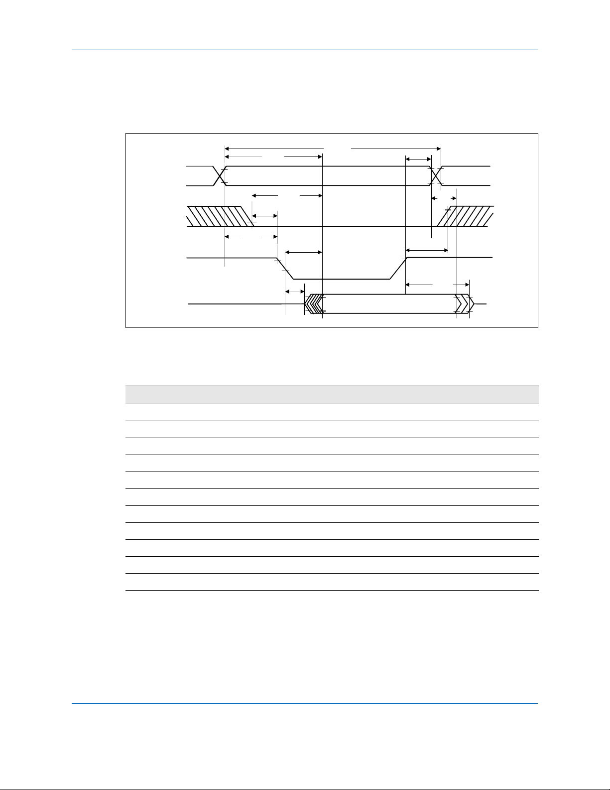
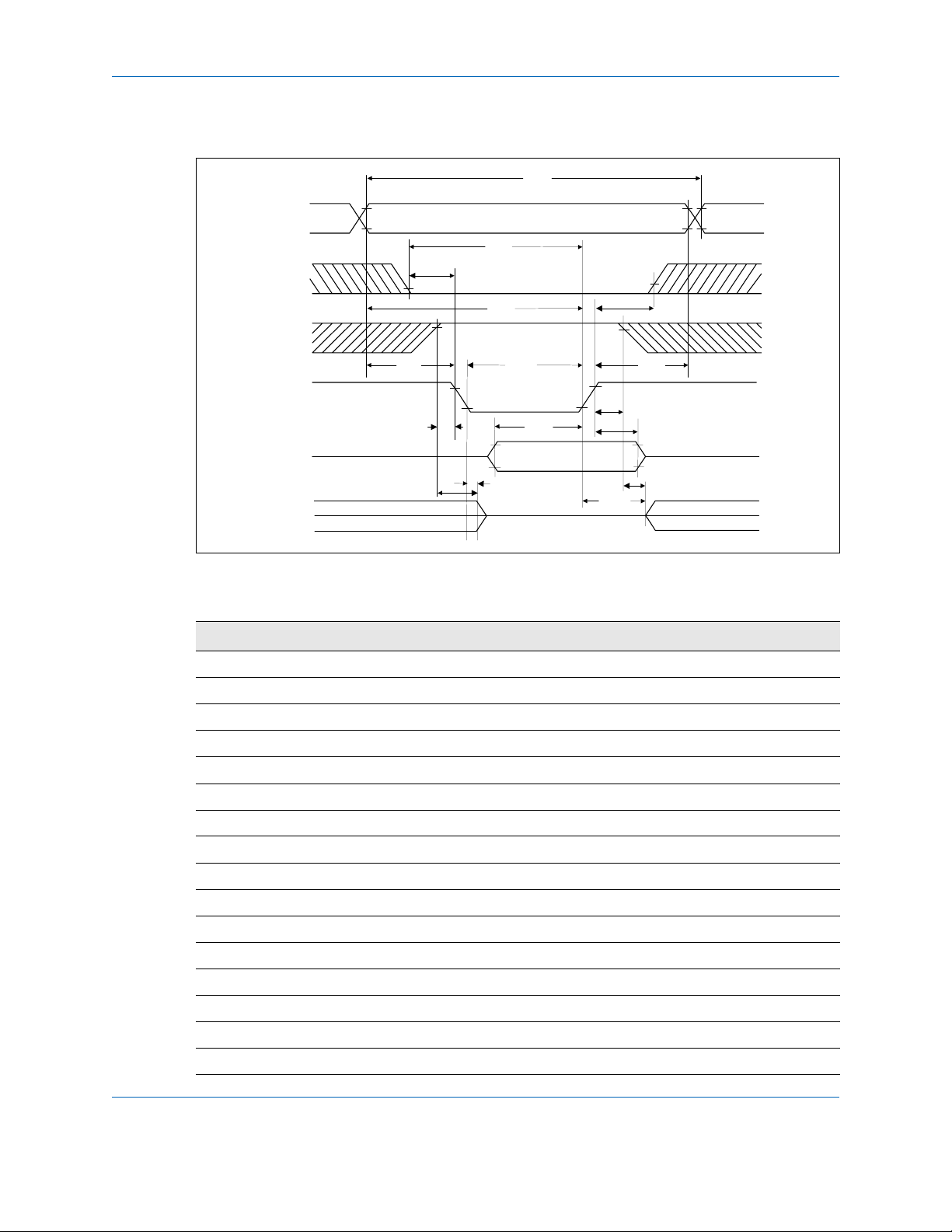
Attribute and Common Memory Read Timing
____
A[10::0],REG
__
CE
__
OE
D[15::0]
tAVWL
tELWL
tEN(OE)
tA(A)
tA(CE)
A(OE)
t
tRC
tGHAX
tAXQX
tGHEH
tDIS(OE)
Figure 2: Attribute and Common Memory Read Timing Diagram
Table 12: Attribute and Common Memory Read Timing
Symbol Parameter Minimum Maximum Units
t
RC
t
(A) Address Access Time - 100 ns
A
t
(CE) Card Enable Access Time - 100 ns
A
t
(OE) Output Enable Access Time - 50 ns
A
t
(OE) Output Disable Time from OE - 50 ns
DIS
(OE) Output Enable Time from OE 5 - ns
t
EN
t
AXQX
t
AVW L
t
AXQX
t
ELWL
t
GHEH
Read Cycle Time 100 - ns
Data Valid from Address Change 0 - ns
Address Setup Time 10 - ns
Address Hold Time 15 - ns
Card Enable Setup Time before OE 0 - ns
Card Enable Hold Time following OE 15 - ns
SILICONSYSTEMS PROPRIETARY
This document and the information contained within it is confidential and proprietary to SiliconSystems, Inc.
3521P-02DSR PAGE 17 FEBRUARY 2, 2009
All unauthorized use and/or reproduction is prohibited.
Page 28
ELECTRICAL SPECIFICATION SSD-PXXX(I)-3521 DATA SHEET
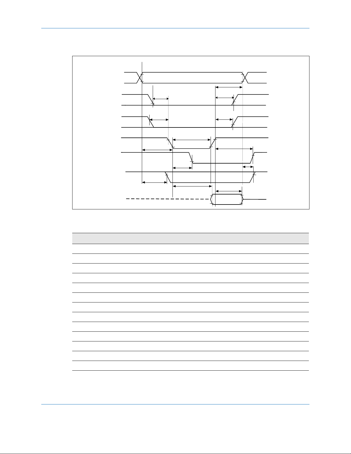
Attribute and Common Memory Write Timing
tWR
____
A[10::0],REG
tELWH
tAVWL
tWLOL
tELWL
tAVWH
tWLWH tWHAX
tWHOL
tDVWH
tGHEH
tWHDX
__
CE
__
OE
___
WE
D[15:0](Dout)
D[15:0](Dout)
tOLWH
tWLQZ
tWHOX
tOHDX
Figure 3: Attribute and Common Memory Write Timing Diagram
Table 13: Attribute and Common Memory Write Timing
Symbol Parameter Minimum Maximum Units
t
WR
t
WLWH
t
AVW L
t
AVW H
t
ELWH
t
WHDX
t
WHAX
t
WLQZ
t
OLWH
t
WHOX
t
OHDX
t
WLOL
t
WHOL
t
ELWL
t
GHEH
t
DVWH
Write Cycle Time 100 - ns
Write Pulse Width 60 - ns
Address Setup Time 10 - ns
Address Setup Time for WE 70 - ns
Card Enable Setup Time for WE 70 - ns
Data Hold Time 10 - ns
Write Recover Time 15 - ns
Output Disable Time from WE - 75 ns
Output Disable Time from OE - 100 ns
Output Enable Time from WE 5 - ns
Output Enable Time from OE 5 - ns
Output Enable Setup for WE 10 - ns
Output Enable Hold from WE 10 - ns
Card Enable Setup Time before WE 0 - ns
Card Enable Hold Time from WE 15 - ns
Data Setup Time 40 - ns
SILICONSYSTEMS PROPRIETARY
This document and the information contained within it is confidential and proprietary to SiliconSystems, Inc.
3521P-02DSR PAGE 18 FEBRUARY 2, 2009
All unauthorized use and/or reproduction is prohibited.
Page 29
ELECTRICAL SPECIFICATION SSD-PXXX(I)-3521 DATA SHEET
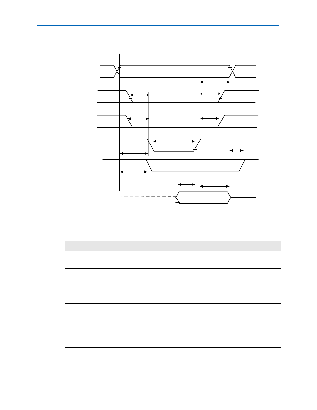
I/O Access Read Timing
A[10:: 0]
tGHAX
tRHIGH
tCHIGH
tIGHINH
tAXISH
tIGHQX
____
REG
__
CE
___
IORD
______
INPACK
______
IOIS16
D[15::0]
tRLIGL
tCLIGL
tIGLIGH
tAVIGL
tIGLINL
tAVISL
tDVRL
Figure 4: I/O Access Read Timing Diagram
Table 14: I/O Access Read Timing
Symbol Parameter Minimum Maximum Units
t
DVRL
t
IGHQX
t
IGLIGH
t
AVI GL
t
GHAX
t
CLIGL
t
CHIGH
t
RLIGL
t
RHIGH
t
IGLINL
t
IGHINH
t
AVI S L
t
AXISH
Data Delay after IORD - 50 ns
Data Hold following IORD 5 - ns
IORD Pulse Width 65 - ns
Address Setup before IORD 25 - ns
Address Hold following IORD 10 - ns
CE Setup before IORD 5 - ns
CE Hold following IORD 10 - ns
REG Setup before IORD 5 - ns
REG Hold following IORD 0 - ns
INPACK Delay falling from IORD - (1) ns
INPACK Delay Rising from IORD - (1) ns
IOIS16 Delay Falling from Address - (1) ns
IOIS16 Delay Rising from Address - (1) ns
Note: (1) IOIS16 and INPACK are not supported.
SILICONSYSTEMS PROPRIETARY
This document and the information contained within it is confidential and proprietary to SiliconSystems, Inc.
3521P-02DSR PAGE 19 FEBRUARY 2, 2009
All unauthorized use and/or reproduction is prohibited.
Page 30
ELECTRICAL SPECIFICATION SSD-PXXX(I)-3521 DATA SHEET
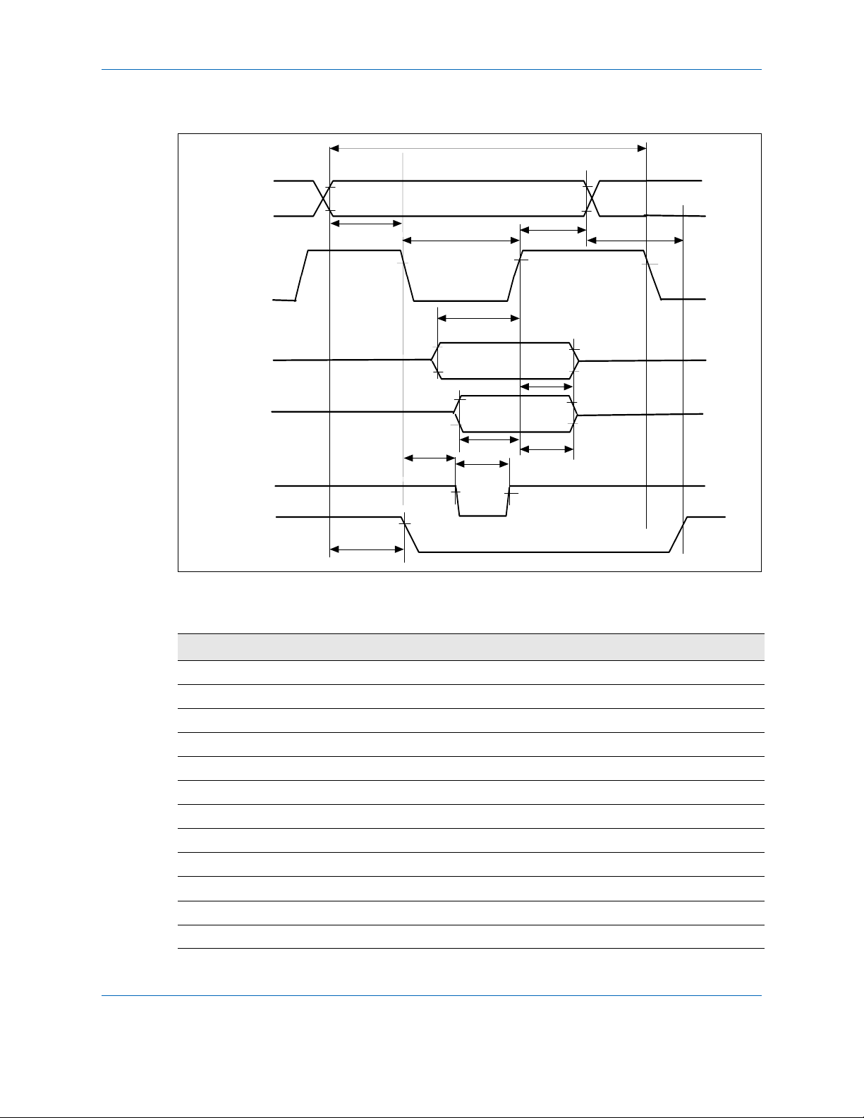
I/O Access Write Ti ming
A[10::0]
____
REG
__
CE
_____
IOWR
______
IOIS16
D[15::0]
tRLIGL
tCLIGL
tIGLIGH
tAVIGL
tAVISL
tIGHQX
tAXIGH
tRHIGH
tCHIGH
tIGHDX
Figure 5: I/O Access Write Timing Diagram
tAXISH
Table 15: I/O Access Write Timing
Symbol Parameter Minimum Maximum Units
t
IGHDX
t
IGHQX
t
IGLIGH
t
AVI GL
t
AXIGH
t
CLIGL
t
CHIGH
t
RLIGL
t
RHIGH
t
AVI S L
t
AXISH
Data Hold following IOWR 5 - ns
Data Setup before IOWR 20 - ns
IOWR Pulse Width 65 - ns
Address Setup before IOWR 25 - ns
Address Hold following IOWR 10 - ns
CE Setup before IOWR 5 - ns
CE Hold following IOWR 10 - ns
REG Setup before IOWR 5 - ns
REG Hold following IOWR 0 - ns
IOIS16 Delay Falling from Address - (1) ns
IOIS16 Delay Rising from Address - (1) ns
Note: (1) IOIS16 and INPACK are not supported.
SILICONSYSTEMS PROPRIETARY
This document and the information contained within it is confidential and proprietary to SiliconSystems, Inc.
All unauthorized use and/or reproduction is prohibited.
3521P-02DSR PAGE 20 FEBRUARY 2, 2009
Page 31
ELECTRICAL SPECIFICATION SSD-PXXX(I)-3521 DATA SHEET
True IDE Read/Write Access Timing
tIC L
ADDRESS Val i d
CS0, CS1, DA[2::0]
tAX 16H
tDXW H
____ _____
DIOR,DIOW
WRI T E
DD[1 5:: 00]
READ
DD[1 5:: 00]
IORDY
______
IOIS16
tAVRWL
tAV16L
tIO S T
tRWPW
tDVW L
tDVRL
tIO P W
tAXRWH
tDXRH
Figure 6: True IDE Read/Write Access Timing Diagram
Table 16: True IDE Read/Write Access Timing
Symbol Parameter Minimum Maximum Units
t
ICL
t
AVRWL
t
RWPW
t
DVWL
t
DXWH
t
DVRL
t
DXRH
t
AV1 6L
t
AX16H
t
AXRWH
t
IOST
t
IOPW
Cycle Time 100 - ns
Address Valid to DIOR,DIOW Setup Time 15 - ns
DIOR, DIOW Pulse Width 65 - ns
DIOW Data Setup Time 20 - ns
DIOW Data Hold Time 5 - ns
DIOR Data Setup Time 15 - ns
DIOR Data Hold Time 5 - ns
Address Valid to IOCS16 Assertion - (1) ns
Address Valid to IOCS16 Negation - (1) ns
DIOW,DIOR to Address Valid Hold Time 10 - ns
IORDY Setup Time - (1) ns
IORDY Pulse Width - (1) ns
Note: (1) IOIS16 and INPACK are not supported.
SILICONSYSTEMS PROPRIETARY
This document and the information contained within it is confidential and proprietary to SiliconSystems, Inc.
All unauthorized use and/or reproduction is prohibited.
3521P-02DSR PAGE 21 FEBRUARY 2, 2009
Page 32
ELECTRICAL SPECIFICATION SSD-PXXX(I)-3521 DATA SHEET
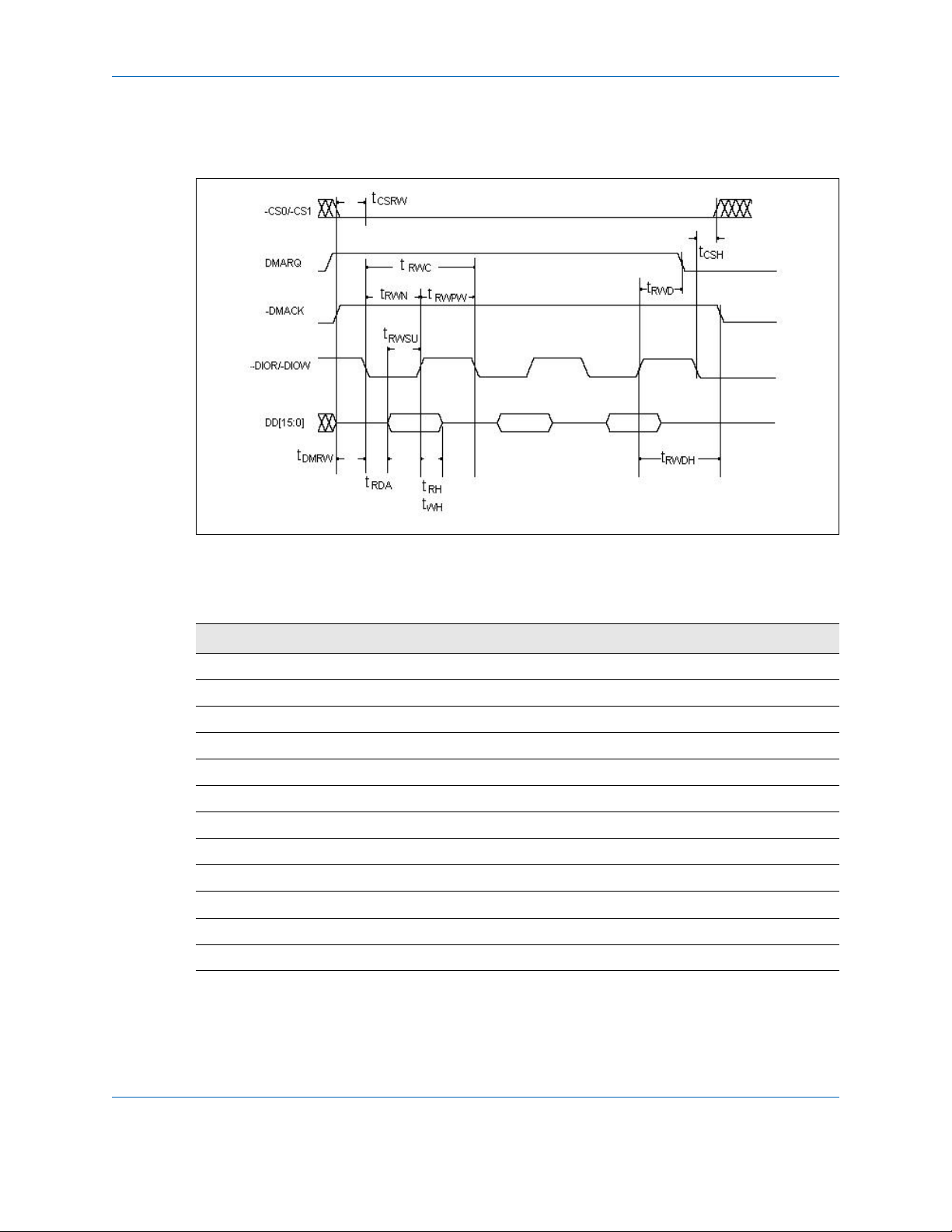
True IDE Multiword DMA Read/Write Access Timing
This function does not apply to SiliconDrives that have DMA disabled.
Figure 7: True IDE Multiword DMA Read/Write Access Timing
Table 17: True IDE Multiword DMA Read/Write Access Timing
Symbol Parameter Minimum Maximum Units
t
RWC
t
RWPW
t
RDA
t
RWSU
t
WH
t
RH
t
DMRW
t
RWDH
t
RWN
t
RWD
t
CSRW
t
CSH
Cycle Time (mode 2) 100 - ns
DIOR/DIOW Pulse Width 65 - ns
DIOR Data Access - 50 ns
DIOR/DIOW Data Setup Time 15 - ns
DIOW Data Hold Time 5 - ns
DIOR Data Hold Time 5 - ns
DMACK to DIOR/DIOW Setup Time 0 - ns
DIOR/DIOW to DMACK Hold Time 5 - ns
DIOR/DIOW negated Pulse Width 25 - ns
DIOR/DIOW to DMARQ Delay - 35 ns
CS(1:0) valid to DIOR/DIOW 10 - ns
CS(1:0) Hold Time 10 - ns
SILICONSYSTEMS PROPRIETARY
This document and the information contained within it is confidential and proprietary to SiliconSystems, Inc.
3521P-02DSR PAGE 22 FEBRUARY 2, 2009
All unauthorized use and/or reproduction is prohibited.
Page 33

ATTRIBUTE MEMORY DESCRIPTION AND OPERATION SSD-PXXX(I)-3521 DATA SHEET
ATTRIBUTE MEMORY DESCRIPTION AND OPERATION
The attribute memory plane can be read or written to by asserting the REG#
signal, qualified by the appropriate combination of CE1#, OE#, and WE#. An
attribute memory map describing the type and location of the information
maintained in the attribute memory plane is provided in "Attribute Memory
Map" on page 25.
With respect to SiliconDrive CF, attribute memory consists of two sections:
• Card Information Structure (CIS), which contains a description of the Card’s
capabilities and specifications.
• Function Configuration Registers (FCRs), which consists of four registers,
that can be read or written to by a host to configure the Card for specific
purposes.
ATTRIBUTE MEMORY READ OPERATIONS
Attribute memory read operations are enabled by asserting REG#, OE#, and
CE1# low. Odd byte read operations from the attribute memory plane are not
valid.
Table 18: Attribute Memory Read Operations
Function
Mode
REG# CE1# CE2# A0 OE# WE# D[15:8] D[7:0]
Standby L HHXXXHigh-ZHigh-Z
Byte Access L L H L L H High-Z Even
L H L H L H High-Z Not Valid
Word Access L L L X L H Not Valid Even
Odd Byte
L L H X H H Not Valid High-Z
Only Access
SILICONSYSTEMS PROPRIETARY
This document and the information contained within it is confidential and proprietary to SiliconSystems, Inc.
3521P-02DSR PAGE 23 FEBRUARY 2, 2009
All unauthorized use and/or reproduction is prohibited.
Page 34

ATTRIBUTE MEMORY DESCRIPTION AND OPERATION SSD-PXXX(I)-3521 DATA SHEET
ATTRIBUTE MEMORY WRITE OPERATIONS
Attribute memory write operations are enabled by asserting REG#, WE#, and
CE1# low. Odd byte write operations from the attribute memory plane are not
valid.
Table 19: Attribute Memory Write Operations
Function
Mode
REG# CE1# CE2# A0 OE# WE# D[15:8] D[7:0]
Standby L HHXXXHigh-ZHigh-Z
Byte Access L L H L H L High-Z Even
L H L H H L High-Z Not Valid
Word Access L L L X H L Not Valid Even
Odd Byte
L L HXHHNot ValidHigh-Z
Only Access
SILICONSYSTEMS PROPRIETARY
This document and the information contained within it is confidential and proprietary to SiliconSystems, Inc.
3521P-02DSR PAGE 24 FEBRUARY 2, 2009
All unauthorized use and/or reproduction is prohibited.
Page 35

ATTRIBUTE MEMORY DESCRIPTION AND OPERATION SSD-PXXX(I)-3521 DATA SHEET
ATTRIBUTE MEMORY MAP
As stated earlier, the Attribute Memory plane is comprised of two components,
the CIS and the FCRs. The following tables detail the type, location, and read/
write requirements for each of the four FCRs maintained in the attribute
memory plane.
Table 20: Attribute Memory Map
Register Operation Addr CE1# REG# WE# OE#
Card Information Structure Read X 0 0 1 0
Write X0001
Configuration Option Read 200h 0 0 1 0
Write 200h0001
Card Configuration and
Read 202h 0 0 1 0
Status
Write 202h0001
Pin Replacement Read 204h 0 0 1 0
Write 204h0001
Socket and Copy Read 206h 0 0 1 0
Write 206h0001
SILICONSYSTEMS PROPRIETARY
This document and the information contained within it is confidential and proprietary to SiliconSystems, Inc.
3521P-02DSR PAGE 25 FEBRUARY 2, 2009
All unauthorized use and/or reproduction is prohibited.
Page 36
ATTRIBUTE MEMORY DESCRIPTION AND OPERATION SSD-PXXX(I)-3521 DATA SHEET
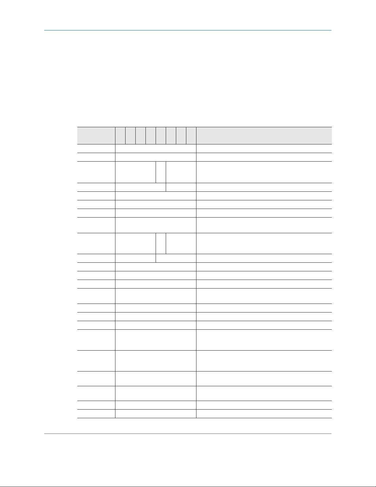
CARD INFORMATION STRUCTURE
The CIS is data that describes the SiliconDrive CF, and is described by the
CFA standard. This information can be used by the host system to determine a
number of things about the Card that has been inserted. For information
regarding the exact nature of this data and how to design the host software to
interpret it, refer to the PC Card Standard Metaformat Specification.
Table 21: Card Information Structure
Attribute
Offset
00h 01h CISTPL_DEVICE Device information tuple Tuple code
02h 03h - Link length is 3 bytes Link to next tuple
04h D9h Device Type
0 6 h 0 1 h 1 X 2 K 2 K B of a d d r es s s p ac e D e v ic e s i ze
08h FFh List End Marker End of device END marker
0Ah 1Ch CISTPL_DEVICE_OC Other conditions device in tuple code Tuple code
0Ch 04h TPL_LINK Link length is 4 bytes Link to next tuple
0Eh 02h EXT Reserved V
10h D9h Device Type W
12h 01h 1x 2K units 2KB of address space Device size
14h FFh List End Marker End of device End marker
16h 18h CISTPL_JEDEC_C JEDEC ID common memory Tuple code
18h 02h TPL_LINK Link length is 2 bytes Link to next tuple
1Ah DFh PCMCIA Manufacturer’s JEDEC Manufacturer’s ID code
1Ch 01h PCMCIA JEDEC Device Code Second byte of JEDEC ID -
1Eh 20h CISTPL_MANFID Manufacturer’s ID code Tuple code
20h 04h TPL_LINK - -
22h 00h Low Byte of PCMCIA Manufacturer’s
24h 00h High Byte of PCMCIA
26h 00h Low Byte of Product Code Manufacturer’s code for SiliconDrive CF Low byte of the
28h 00h High Byte of Product Code Manufacturer’s code for SiliconDrive CF High byte of the
2Ah 21h CISTPL_FUNCID Function ID tuple Tuple code
2Ch 02h TPL_LINK Link length is 2 bytes Link to next tuple
Data 7 6 5 4 3 2 1 0 Description of Contents CIS Function
Code
W1Device
Dh = I/O
MWAIT
P
S
Code
Manufacturer’s Code
Speed
CC
Device
Speed
• I/O device
•No WP
• Speed = 100ns
1
3V, wait is Not Used Other conditions
• Device type = DH: I/O
• Device WPS = 1: No WP
• Device speed = 1: 250ns
-
JEDEC manufacturer’s ID Low byte of
Code of 0, because the other byte is the
JEDEC 1 byte manufacturer’s ID
• Device ID
•WPS
• Device speed
information field
-
JEDEC ID
manufacturer’s
code
High byte of the
manufacturer’s
code
product code
product code
SILICONSYSTEMS PROPRIETARY
This document and the information contained within it is confidential and proprietary to SiliconSystems, Inc.
3521P-02DSR PAGE 26 FEBRUARY 2, 2009
All unauthorized use and/or reproduction is prohibited.
Page 37
ATTRIBUTE MEMORY DESCRIPTION AND OPERATION SSD-PXXX(I)-3521 DATA SHEET
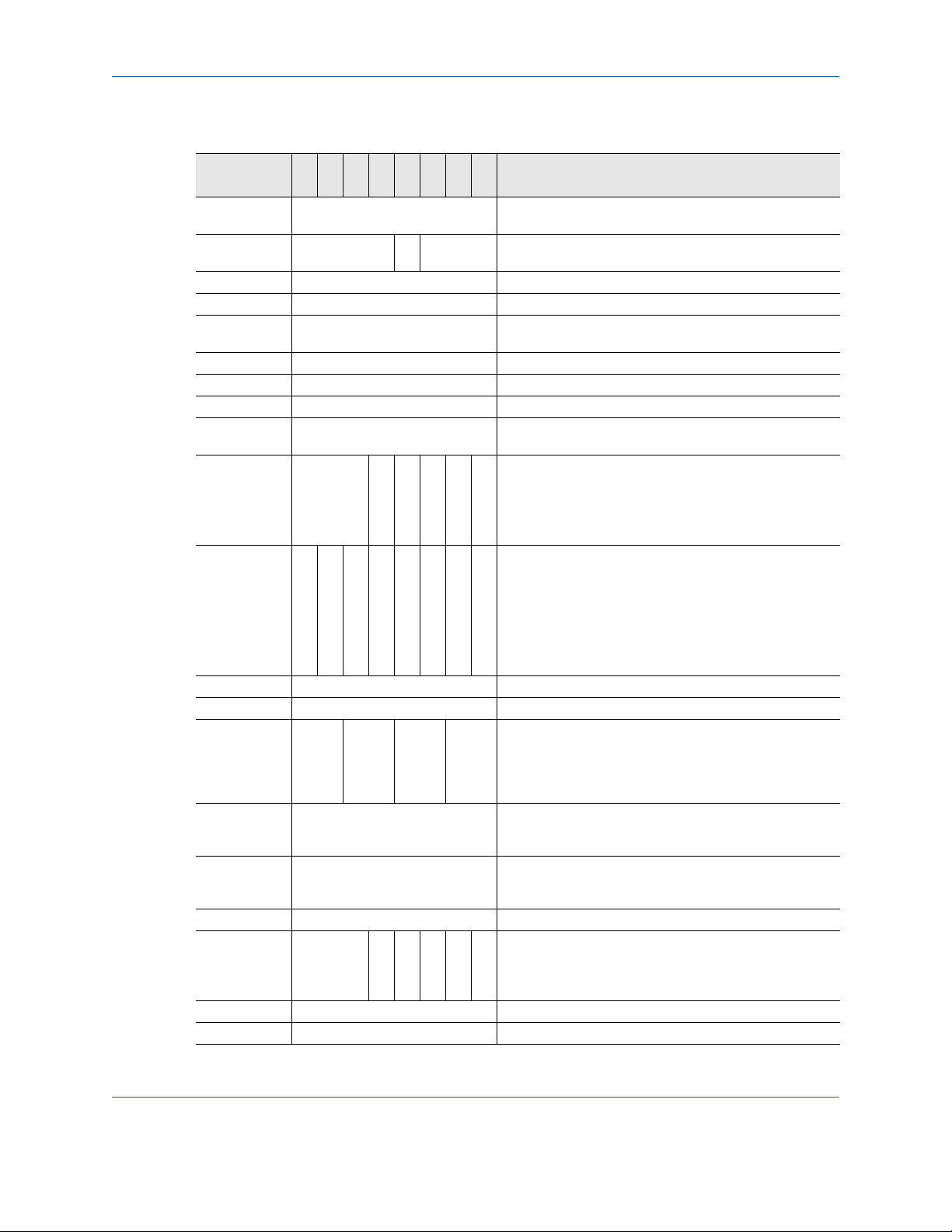
Table 21: Card Information Structure (Continued)
Attribute
Offset
2Eh 04h TPLFID_FUNCTION = 04H Disk function, which may be silicon or
30h 01h Reserved R P • R = 0: No BIOS ROM
32h 22h CISTPL_FUNCE Function extension tuple Tuple code
34h 02h TPL_LINK Link length is 2 bytes Link to next tuple
36h 01h Disk Function Extension Tuple Type Disk interface type Extension tuple type
38h 01h Disk Interface Type PC Card interface type Interface type
3Ah 22h CISTPL_FUNCE Function extension tuple Tuple code
3Ch 03h TPL_LINK Link length is 3 bytes Link to next tuple
3Eh 02h Disk Function Extension Tuple Type Basic PCMCIA-ATA extension tuple Extension tuple type
40h 04h Reserved D U S V No Vpp, silicon, single drive
42h 07h R I E N P3 P2 P1 P0 • P0: Sleep mode supported
44h 1Ah CISTPL_CONFIG Configuration tuple Tuple code
46h 05h TPL_LINK Link length is 5 bytes Link to next tuple
48h 01h RAS RMS RAS - • RFS: Reserved
4Ah 07h TPCC_LAST Entry with configuration index of 7 is final
4Ch 00h TPCC_RADR (LSB) Configuration registers are located at
4Eh 02h TPCC_RADR (MSB) - -
50h 0Fh Reserved S P C I - • I: Configuration index
52h 1Bh CISTPL_TABLE_ENTRY Configuration table entry tuple Tuple code
54h 0Bh TPL_LINK Link length is 11 bytes Link to next tuple
Data 7 6 5 4 3 2 1 0 Description of Contents CIS Function
PC Card function
removable
• P = 1: Configure card at power-on
• V = 0: No Vpp required
• S = 0: Silicon
• U = 1: Unique serial number
• D = 0: Single drive on Card
• P1: Standby mode supported
• P2: Idle mode supported
• P3: Drive auto power control
• N: Some configuration excludes 3X7
• E: Index bit is emulated
• I: Twin IOIS16# data register only
•R: Reserved
• RMS: TPCC RMSK size -1 = 0
• RAS: TPCC_RADR size -1 = 1
• 1-byte register mask
• 2-byte configuration base address
entry in table
200H in REG space
• C: Configuration and status
• P: Pin replacement
• S: Socket and copy
code
System initialization
byte
for disk
for disk
Basic ATA option
parameters byte 1
Basic ATA option
parameters byte 2
Size of fields byte
TPCC_SZ
Last entry of
configuration
registers
Location of
configuration
registers
Configuration
registers present
mask
TPCC_RMSK
SILICONSYSTEMS PROPRIETARY
This document and the information contained within it is confidential and proprietary to SiliconSystems, Inc.
3521P-02DSR PAGE 27 FEBRUARY 2, 2009
All unauthorized use and/or reproduction is prohibited.
Page 38
ATTRIBUTE MEMORY DESCRIPTION AND OPERATION SSD-PXXX(I)-3521 DATA SHEET
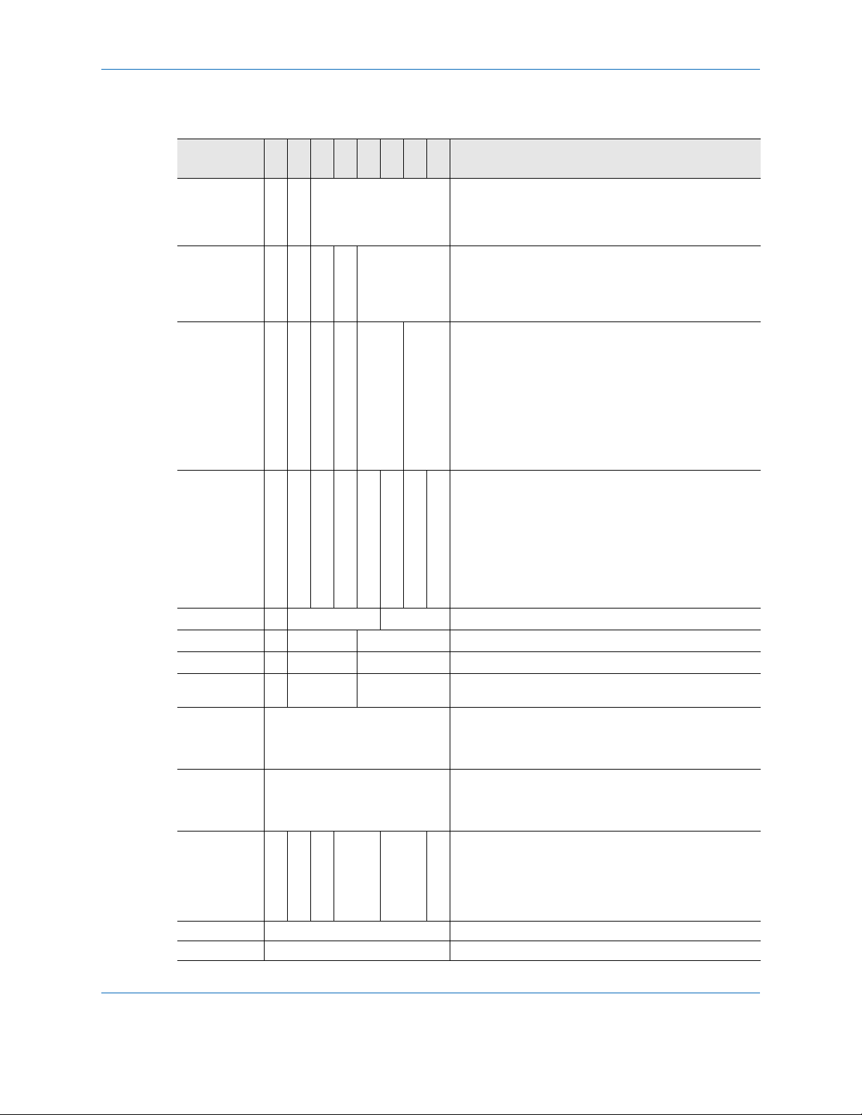
Table 21: Card Information Structure (Continued)
Attribute
Offset
56h C0h I D Configuration index Memory-mapped I/O configuration
58h C0h W R P B Interface Type • W = 0: Wait not used
5Ah A1h M MS IR IO T P • M = 1: Miscellaneous information
5Ch 27h R DI PI AI SI HV LV NV Nominal voltage only follows
5Eh 55h X Mantissa Exponent Nominal voltage = 5V VCC nominal value
60h 4Dh X Mantissa Exponent V
62h 5Dh X Mantissa Exponent V
64h 75h X Mantissa Exponent Maximum average current over 10ms is
66h 08h Length in 256 bytes pages (LSB) Length of memory space is 2KB Memory space
68h 00h Length in 256 bytes pages (MSB) Length of memory space is 2KB Memory space
6Ah 21h X R P RO AT - • X = 0: No more miscellaneous fields
6Ch 1Bh CISTPL_TABLE_ENTRY Configuration table entry tuple Tuple code
6Eh 06h TPL_LINK Link length is 6 bytes Link to next tuple
Data 7 6 5 4 3 2 1 0 Description of Contents CIS Function
Configuration table
• I = 1: Interface byte follows
• D = 1: Default entry
• Configuration index = 0
• R = 1: Ready active
• P = 0: WP used
• B = 0: BVD1 and BVD2 not used
• IF type = 0: Memory interface
present
• MS = 01: Memory space information
single 2-byte length
• IR = 0: No interrupt information
present
• IO = 0: No I/O port information
present
• T = 0: No timing information present
•P = 1: V
•R: Reserved
• DI: Powerdown current information
• PI: Peak current information
• AI: Average current information
• SI: Static current information
• HV: Maximum voltage information
• LV: Minimum voltage information
• NV: Nominal voltage information
nominal 4.5V VCC minimum value
CC
nominal 5.5V VCC maximum value
CC
80mA
•R: Reserved
• P = 1: Powerdown supported
• RO = 0: Not read only mode
• A = 0: Audio not supported
• T = 0: Single drive
only information
CC
index byte
TPCE_INDX
Interface description
field TPCE_IF
Feature selection
byte TPCE_FS
Power parameters
for V
CC
Maximum average
current
description
structures
(TPCE_MS)
description
structures
(TPCE_MS)
Miscellaneous
features field
TPCE_MI
SILICONSYSTEMS PROPRIETARY
This document and the information contained within it is confidential and proprietary to SiliconSystems, Inc.
3521P-02DSR PAGE 28 FEBRUARY 2, 2009
All unauthorized use and/or reproduction is prohibited.
Page 39
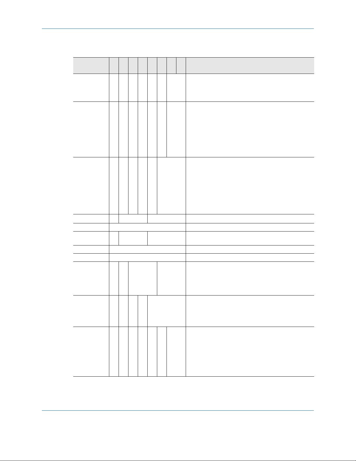
ATTRIBUTE MEMORY DESCRIPTION AND OPERATION SSD-PXXX(I)-3521 DATA SHEET
Table 21: Card Information Structure (Continued)
Attribute
Offset
70h 00h I D IR IQ T P - Memory-mapped I/O configuration
72h 01h M MS IR IO T P - • M = 0: No miscellaneous information
74h 21h R DI PI AI SI HV/LV/NV Nominal voltage only follows
76h B5h X Mantissa Exponent Nominal voltage = 3.0 V VCC nominal value
78h 1Eh Extension +0.3 V Extension byte
7Ah 4Dh X Mantissa Exponent Maximum average current over 10ms is
7Ch 1Bh CISTPL_TABLE_ENTRY Configuration table entry tuple Tuple code
7Eh 0Dh TPL_LINK Link length is 10 bytes Link to next tuple
80h C1h I D Configuration INDEX Contiguous I/O mapped ATA registers
82h 41h W R P B Interface Type • W = 0: Wait not used
84h 99h M MS IR IO T P - • M = 1: Miscellaneous information
Data 7 6 5 4 3 2 1 0 Description of Contents CIS Function
Configuration table
• I = 0: No interface byte
• D = 0: No default entry
• Configuration index = 0
• MS = 00: No memory space
information
• IR = 0: No interrupt information
present
• IO = 0: No I/O port information
present
• T = 0: No timing information present
•P = 1: V
•R: Reserved
• DI: Powerdown current information
• PI: Peak current information
• AI: Average current information
• SI: Static current information
• HV: Maximum voltage information
• LV: Minimum voltage information
• NV: Nominal voltage information
45 mA
configuration
• I = 1: Interface byte follows
• D = 1: Default entry
• Configuration index = 1
• R = 1: Ready active
• P = 0: WP not used
• B = 0: BVS1 and BVD2 not used
• IF type = 1: I/O interface
present
• MS = 00: No memory space
information
• IR = 1: Interrupt information present
• IO = 1: I/O port information present
• T = 0: No timing information present
•P = 1: V
only information
CC
only information
CC
index byte
TPCE_INDX
Feature selection
byte
TPCE_FS
Power parameters
for V
CC
Maximum average
current
Configuration table
index byte
TPCE_INDX
Interface description
field TPCE_IF
Feature selection
byte TPCE_FS
SILICONSYSTEMS PROPRIETARY
This document and the information contained within it is confidential and proprietary to SiliconSystems, Inc.
3521P-02DSR PAGE 29 FEBRUARY 2, 2009
All unauthorized use and/or reproduction is prohibited.
Page 40
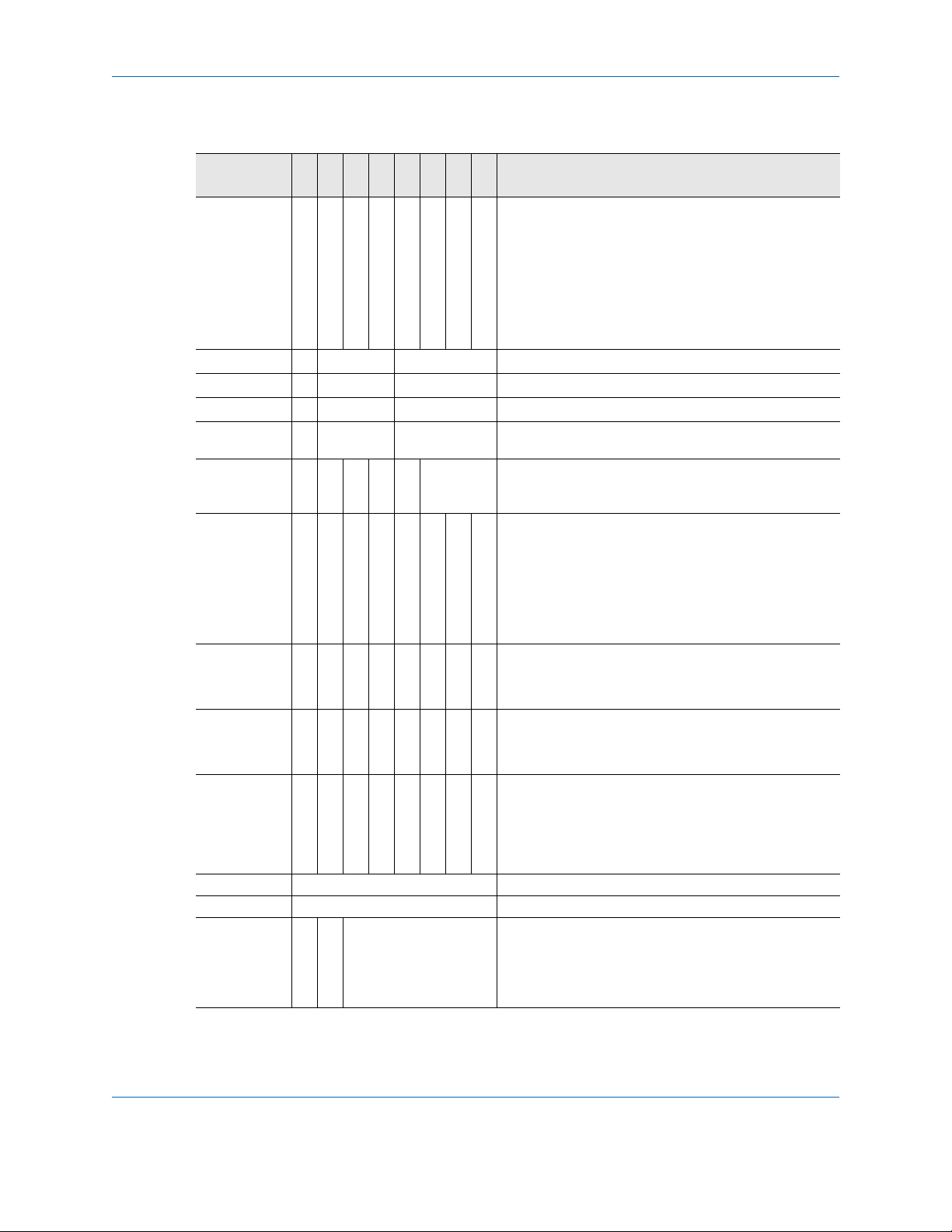
ATTRIBUTE MEMORY DESCRIPTION AND OPERATION SSD-PXXX(I)-3521 DATA SHEET
Table 21: Card Information Structure (Continued)
Attribute
Offset
86h 27h R DI PI AI SI HV LV NV Nominal voltage only follows
88h 55h X Mantissa Exponent Nominal voltage = 5V VCC nominal value
8Ah 4Dh X Mantissa Exponent V
8Ch 5Dh X Mantissa Exponent V
8Eh 75h X Mantissa Exponent Maximum average current over 10ms is
90h 64h R S E I O AddrLine • S = 1: 16-bit hosts supported
92h F0h S P L M V B I N • S = 1: Share logic active
94h FFh IR IR IR IR IR IR IR IR SiliconSystems recommends the IRQ
96h FFh IR IR IR IR IR IR IR IR SiliconSystems recommends routing to
98h 21h X R P R O A T - • X = 0: No more miscellaneous fields
9Ah 1Bh CISTPL__TABLE_ENTRY Configuration table entry tuple Tuple code
9Ch 06h TPL_LINK Link length is 6 bytes Link to next tuple
9Eh 01h I D Configuration Index Contiguous I/O mapped ATA registers
Data 7 6 5 4 3 2 1 0 Description of Contents CIS Function
Power parameters
for V
CC
Maximum average
current
I/O space
description field
TPCE_IO
Interrupt request
description structure
TPCE_IR
Mask extension
byte 1 TPCE_IR
Mask extension
byte 2 TPCE_IR
Miscellaneous
features field
TPCE_MI
Configuration table
index
Byte TPCE_INDX
QQQQQQQQ
76543210
QQQQQQQQ
15 14 13 12 11 10 9 8
•R: Reserved
• DI: Powerdown current information
• PI: Peak current information
• AI: Average current information
• SI: Static current information
• HV: Maximum voltage information
• LV: Minimum voltage information
• NV: Nominal voltage information
nominal 4.5V VCC minimum value
CC
nominal 5.5V VCC maximum value
CC
80mA
• E = 1: 8-bit hosts supported
• IO AddrLine: 4 lines decoded
• P = 1: Pulse mode IRQ supported
• L = 1: Level mode IRQ supported
• M = 1: Bit mask of IRQs present
• V = 0: No vender unique IRQ
• B = 0: No bus error IRQ
• I = 0: No IO check IRQ
• N = 0: No NMI
level to be routed 0 to 15
any normal, maskable IRQ.
•R: Reserved
• P = 1: Powerdown supported
• RO = 0: Not read only mode
• A = 0: Audio not supported
• T = 0: Single drive
configuration
• I = 0: No Interface byte
• D = 0: No Default entry
• Configuration index = 1
SILICONSYSTEMS PROPRIETARY
This document and the information contained within it is confidential and proprietary to SiliconSystems, Inc.
3521P-02DSR PAGE 30 FEBRUARY 2, 2009
All unauthorized use and/or reproduction is prohibited.
Page 41
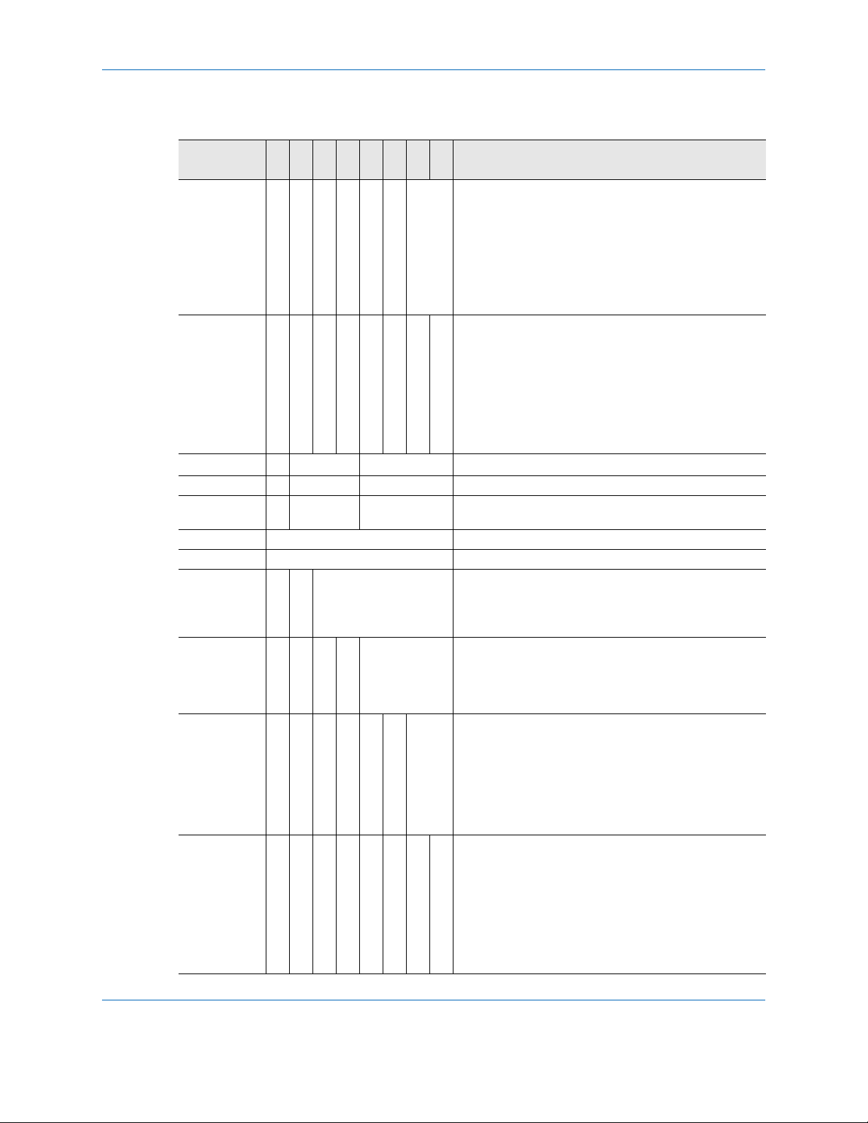
ATTRIBUTE MEMORY DESCRIPTION AND OPERATION SSD-PXXX(I)-3521 DATA SHEET
Table 21: Card Information Structure (Continued)
Attribute
Offset
A0h 01h M MS IR IO T P - • M = 0: No miscellaneous information
A2h 21h R DI PI AI SI HV LV NV Nominal voltage only follows
A4h B5h X Mantissa Exponent Nominal voltage = 3.0V VCC nominal value
A6h 1Eh X Mantissa Exponent +0.3V Extension byte
A8h 4Dh X Mantissa Exponent Maximum average current over 10ms is
AAh 1Bh CISTPL_TABLE_ENTRY Configuration table entry tuple Extension byte
ACh 12h TPL_LINK Link length is 18 bytes Link to next tuple
AEh C2h I D Configuration Index ATA primary I/O mapped configuration
B0h 41h W R P B Interface Type • W = 0: Wait not used
B2h 99h M MS IR IO T P - • M = 1: Miscellaneous information
B4h 27h R DI PI AI SI HV LV NV Nominal voltage only follows
Data 7 6 5 4 3 2 1 0 Description of Contents CIS Function
Feature selection
• MS = 00: No memory space
information
• IR = 0: No interrupt information
present
• IO = 0: No I/O port information
present
• T = 0: No timing information present
•P = 1: V
•R: Reserved
• DI: Powerdown current information
• PI: Peak current information
• AI: Average current information
• SI: Static current information
• HV: Maximum voltage information
• LV: Minimum voltage information
• NV: Nominal voltage information
45mA
• I = 1: Interface byte follows
• D = 1: default entry follows
• Configuration index = 2
• R = 1: Ready active
• P = 0: WP not used
• B = 0: BVS1 and BVD2 not used
• IF type = 1: I/O interface
present
• MS = 00: No memory space
information
• IR = 1: Interrupt information present
• IO = 1: I/O port information present
• T = 0: No timing information present
•P = 1: V
•R: Reserved
• DI: Powerdown current information
• PI: Peak current information
• AI: Average current information
• SI: Static current information
• HV: Maximum voltage information
• LV: Minimum voltage information
• NV: Nominal voltage information
only information
CC
only information
CC
byte TPCE_FS
Power parameters
for V
CC
Maximum average
current
Configuration table
index byte
TPCE_INDX
Interface description
field TPCE_IF
Feature selection
byte TPCE_FS
Power parameters
for V
CC
SILICONSYSTEMS PROPRIETARY
This document and the information contained within it is confidential and proprietary to SiliconSystems, Inc.
3521P-02DSR PAGE 31 FEBRUARY 2, 2009
All unauthorized use and/or reproduction is prohibited.
Page 42
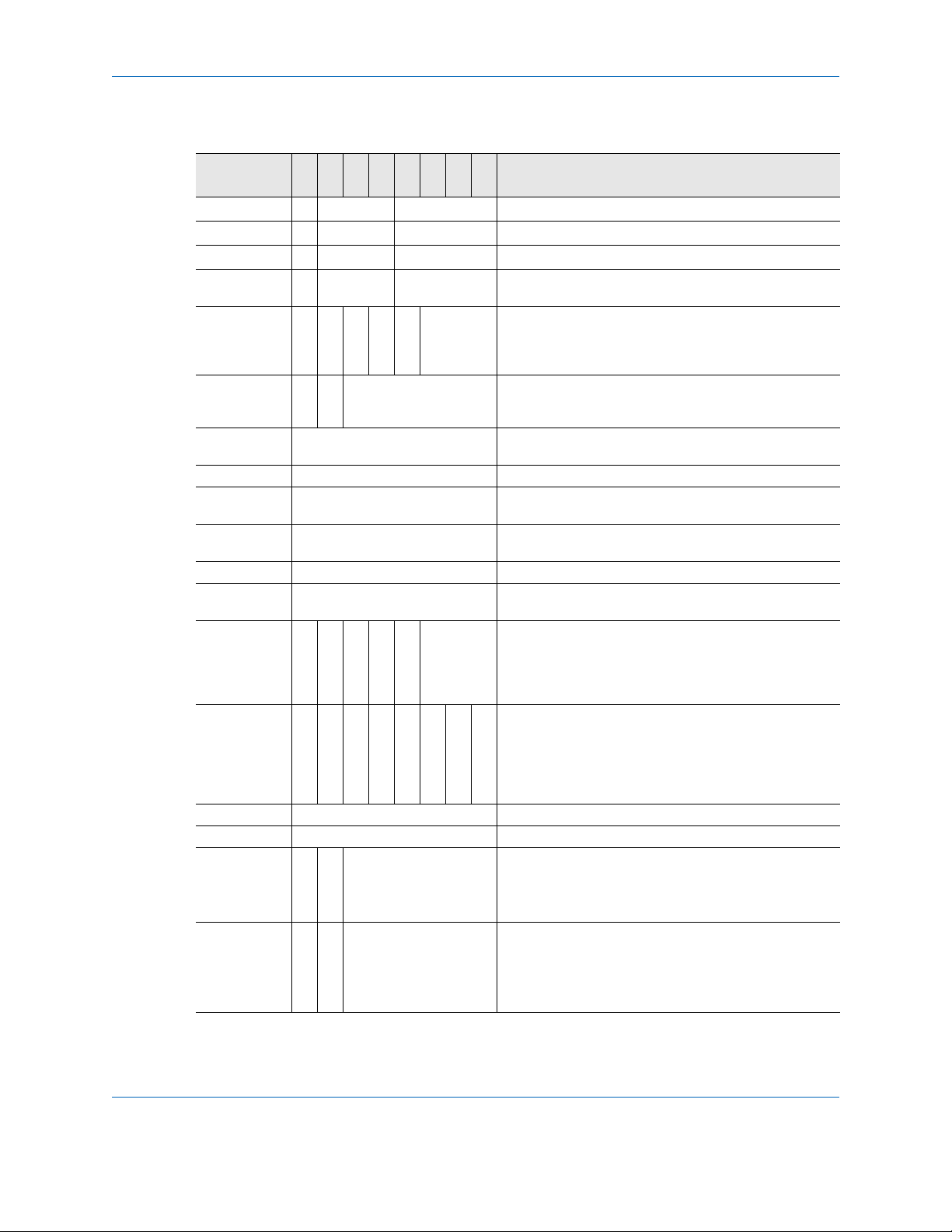
ATTRIBUTE MEMORY DESCRIPTION AND OPERATION SSD-PXXX(I)-3521 DATA SHEET
Table 21: Card Information Structure (Continued)
Attribute
Offset
B6h 55h X Mantissa Exponent Nominal voltage = 5V VCC nominal value
B8h 4Dh X Mantissa Exponent V
BAh 5Dh X Mantissa Exponent V
BCh 75h X Mantissa Exponent Maximum average current over 10ms is
BEh EAh R S E I O AddrLine • R = 1: Range follows
C0h 61h LS AS N Range • LS = 1: Size of lengths is 1 byte
C2h F0h First I/0 Base Address First I/O base address (LSB) First I/O range
C4h 01h First I/0 Base Address First I/O base address (MSB) -
C6h 07h First I/0 Base Address First I/O length -1 First I/O range
C8h F6h Second I/O Base Address Second I/O base address (LSB) Second I/O range
CAh 03h Second I/O Base Address Second I/O base address (MSB)
CCh 01h Second I/O Range Length Second I/O length -1 Second I/O range
CEh EEh S P L M IRQ Level • S = 1: Share logic active
D0h 21h X R P R O A T - • X = 0: No more miscellaneous fields
D2h 1Bh CISTPL_TABLE_ENTRY Configuration table entry tuple Tuple code
D4h 06h TPL_LINK Link length is 6 bytes Link to next tuple
D6h 02h I D Configuration Index ATA primary I/O mapped configuration
D8h 01h I D Configuration Index Contiguous I/O mapped ATA registers
Data 7 6 5 4 3 2 1 0 Description of Contents CIS Function
nominal 4.5V VCC minimum value
CC
nominal 5.5V VCC maximum value
CC
80mA
• S = 1: 16-bit hosts supported
• E = 1: 8-bit hosts supported
IO AddrLines: 10 lines decoded
• AS = 2: Size of address is 2 bytes
• N Range = 1: Address Range-1
• P = 1: Pulse mode IRQ supported
• L = 1: Level mode IRQ supported
• M = 0: Bit mask of IRQs present —
IRQ level is IRQ14
•R: Reserved
• P = 1: Powerdown supported
• RO = 0: Not read only mode
• A = 0: Audio not supported
• T = 0: Single drive
• I = 0: No Interface byte
• D = 0: No Default entry
• Configuration index = 2
configuration
• I = 0: No interface byte
• D = 0: No default entry
• Configuration index = 1
Maximum average
current
I/O space
description field
TPCE_IO
I/O range format
description
address
length
address
length
Interrupt request
description structure
TPCE_IR
Miscellaneous
features field
TPCE_MI
Configuration table
index byte
TPCE_INDX
Configuration table
index byte
TPCE_INDX
SILICONSYSTEMS PROPRIETARY
This document and the information contained within it is confidential and proprietary to SiliconSystems, Inc.
3521P-02DSR PAGE 32 FEBRUARY 2, 2009
All unauthorized use and/or reproduction is prohibited.
Page 43
ATTRIBUTE MEMORY DESCRIPTION AND OPERATION SSD-PXXX(I)-3521 DATA SHEET
Table 21: Card Information Structure (Continued)
Attribute
Offset
DAh 21h M MS IR IO T P - • M = 0: No miscellaneous information
DCh B5h R DI PI AI SI HV LV NV Nominal voltage only follows
DEh 1Eh X Mantissa Exponent Nominal voltage = 3.0V VCC nominal value
E0h 4Dh Extension +0.3V Extension byte
E2h 1Bh CISTPL_TABLE_ENTRY Configuration table entry tuple Tuple code
E4h 12h TPL_LINK Link length is 18 bytes Link to next tuple
E6h C3h M MS IR IO T P - • M = 0: No miscellaneous information
E8h 41h R DI PI AI SI HV LV NV Nominal voltage only follows
EAh 99h M MS IR IO T P - • M = 1: No miscellaneous information
Data 7 6 5 4 3 2 1 0 Description of Contents CIS Function
Feature selection
• MS = 00: No memory space
information
• IR = 0: No interrupt information
present
• IO = 0: No I/O port information
present
• T = 0: No timing information present
•P = 1: V
•R: Reserved
• DI: Powerdown current information
• PI: Peak current information
• AI: Average current information
• SI: Static current information
• HV: Maximum voltage information
• LV: Minimum voltage information
• NV: Nominal voltage information
• MS = 00: No memory space
information
• IR = 0: No interrupt information
present
• IO = 0: No I/O port information
present
• T = 0: No timing information present
•P = 1: V
•R: Reserved
• DI: Powerdown current information
• PI: Peak current information
• AI: Average current information
• SI: Static current information
• HV: Maximum voltage information
• LV: Minimum voltage information
• NV: Nominal voltage information
• MS = 00: No Memory space
information
• IR = 1: No interrupt information
present
• IO = 1: No I/O port information
present
• T = 0: No timing information present
• P = 01: V
only information
CC
only information
CC
only information
CC
byte TPCE_FS
Power parameters
for V
CC
Feature selection
byte TPCE_FS
Power parameters
for V
CC
Feature selection
byte TPCE_FS
SILICONSYSTEMS PROPRIETARY
This document and the information contained within it is confidential and proprietary to SiliconSystems, Inc.
3521P-02DSR PAGE 33 FEBRUARY 2, 2009
All unauthorized use and/or reproduction is prohibited.
Page 44
ATTRIBUTE MEMORY DESCRIPTION AND OPERATION SSD-PXXX(I)-3521 DATA SHEET
Table 21: Card Information Structure (Continued)
Attribute
Offset
ECh 27h R DI PI AI SI HV LV NV Nominal voltage only follows
EEh 55h X Mantissa Exponent Nominal voltage = 5V VCC nominal value
F0h 4Dh X Mantissa Exponent V
F2h 5Dh X Mantissa Exponent V
F4h 75h X Mantissa Exponent Maximum average current over 10ms is
F6h EAh R S E I O AddrLine • R = 1: Range follows
F8h 61h LS AS N Range • LS = 1: Size of lengths is 1 byte
FAh 70h - First I/O base address (LSB) First I/O range
FCh 01h - First I/O base address (MSB) -
FEh 07h - First I/O length -1 First I/O range
100h 76h - Second I/O base address (LSB) Second I/O range
102h 03h - Second I/O base address (MSB) -
104h 01h - Second I/O length Second I/O range
106h EEh S P L M IRQ Level • S = 1: Share logic active
108h 21h X R P R O A T - • X = 0: No more miscellaneous fields
10Ah 1Bh CISTPL_TABLE_ENTRY Configuration table entry tuple Tuple code
10Ch 06h TPL_LINK Link length is 6 bytes Link to next tuple
Data 7 6 5 4 3 2 1 0 Description of Contents CIS Function
Power parameters
for V
•R: Reserved
• DI: Powerdown current information
• PI: Peak current information
• AI: Average current information
• SI: Static current information
• HV: Maximum voltage information
• LV: Minimum voltage information
• NV: Nominal voltage information
nominal 4.5V VCC minimum value
CC
nominal 5.5V VCC maximum value
CC
80mA
• S = 1: 16-bit hosts supported
• E = 1: 8-bit hosts supported
• IO AddrLines: 10 lines decoded
• AS = 2: Size of address is 2 bytes
• N Range = 1: Address range -1
• P = 1: Pulse mode IRQ supported
• L = 1: Level mode IRQ supported
• M = 0: Bit mask of IRQs present —
IRQ level is IRQ14
•R: Reserved
• P = 1: Powerdown supported
• RO = 0: Not read only mode
• A = 0: Audio not supported
• T = 0: Single drive
CC
Maximum average
current
I/O space
description field
TPCE_IO
I/O range format
description
address
length
address
length
Interrupt request
description structure
TPCE_IR
miscellaneous
features field
TPCE_MI
-
SILICONSYSTEMS PROPRIETARY
This document and the information contained within it is confidential and proprietary to SiliconSystems, Inc.
3521P-02DSR PAGE 34 FEBRUARY 2, 2009
All unauthorized use and/or reproduction is prohibited.
Page 45
ATTRIBUTE MEMORY DESCRIPTION AND OPERATION SSD-PXXX(I)-3521 DATA SHEET
Table 21: Card Information Structure (Continued)
Attribute
Offset
10Eh 03h I D Configuration Index ATA primary I/O mapped configuration
110h 01h M MS IR IO T P - • M = 0: No miscellaneous information
112h 21h R DI PI AI SI HV LV NV Nominal voltage only follows
114h B5h X Mantissa Exponent Nominal voltage = 3.0V VCC nominal value
116h 1Eh Extension +0.3V Extension byte
118h 4Dh X Mantissa Exponent Maximum average current over 10ms is
11Ah 1Bh CISTPL_MANFID Manufacturer’s ID code Tuple code
11Ch 04h TPL_LINK Link length is 4 bytes Link to next tuple
11Eh 07h I D Configuration Index AT fixed disk secondary I/O 3.3V
120h 00h M MS IR IO T P - P: Power information type TPCL_FS
Data 7 6 5 4 3 2 1 0 Description of Contents CIS Function
Configuration table
• I = 0: No interface byte
• D = 0: No default entry
• Configuration index = 2
• MS = 00: No memory space
information
• IR = 0: No interrupt information
present
• IO = 0: No I/O port information
present
• T = 0: No timing information present
•P = 1: V
•R: Reserved
• DI: Powerdown current information
• PI: Peak current information
• AI: Average current information
• SI: Static current information
• HV: Maximum voltage information
• LV: Minimum voltage information
• NV: Nominal voltage information
45mA
configuration
only information
CC
index byte
TPCE_INDX
Feature selection
byte TPCE_FS
Power parameters
for V
CC
Maximum average
current
TPCE_INDX
122h 28h - Manufacturer code for SiliconDrive CF Reserved
124h D3h - Manufacturer code for SiliconDrive CF Reserved
126h 14h CISTPL_NO_LINK No link control tuple Tuple code
128h 00h - Link is 0 bytes Link to next tuple
12Ah 15h CISTPL_VERS_1 Level 1 version Tuple code
12Ch 1Ah TPL_LINK Link length is 26h bytes Link to next tuple
12Eh 04h TPPLV1_MAJOR PC Card 2.0/JEIDA4.1 END marker
130h 01h TPPLV1_MINOR PC Card 2.0/JEIDA4.1 Tuple code
132h 53h - S Information string
134h 49h - I -
136h 4Ch - L -
138h 49h - I -
13Ah 43h - C -
SILICONSYSTEMS PROPRIETARY
This document and the information contained within it is confidential and proprietary to SiliconSystems, Inc.
3521P-02DSR PAGE 35 FEBRUARY 2, 2009
All unauthorized use and/or reproduction is prohibited.
Page 46
ATTRIBUTE MEMORY DESCRIPTION AND OPERATION SSD-PXXX(I)-3521 DATA SHEET
Table 21: Card Information Structure (Continued)
Attribute
Offset
13Ch 4Fh - O -
13Eh 4Eh - N -
140h 53h - S -
142h 59h - Y -
144h 53h - S -
146h 54h - T -
14Ah 4Dh - M -
14Ch 53h - S -
14Eh 00h - Space -
150h 56h - V -
152h 45h - E -
154h 52h - R -
156h 32h - 2 -
158h 2Eh - - -
15Ah 30h - 0 -
15Ch 30h - 0 -
160h FFh - - -
Data 7 6 5 4 3 2 1 0 Description of Contents CIS Function
45h - E -
00h - - -
SILICONSYSTEMS PROPRIETARY
This document and the information contained within it is confidential and proprietary to SiliconSystems, Inc.
3521P-02DSR PAGE 36 FEBRUARY 2, 2009
All unauthorized use and/or reproduction is prohibited.
Page 47

ATTRIBUTE MEMORY DESCRIPTION AND OPERATION SSD-PXXX(I)-3521 DATA SHEET
CONFIGURATION OPTION REGISTER (200H)
The Configuration Option register is used to configure the SiliconDrive CF,
define the address decoding, and initiate the software RESET sequence.
Table 22: Configuration Option Register (200h)
Operation
Read/
D
7
SRESET LevIREQ Configuration Index
D
6
D
5
D
4
D
3
D
2
D
1
D
0
Write
Default
0 0 000000
Value
Bit(s) Description
SRESET When set, this bit initiates a software-reset sequence, which
is equivalent to a power-on reset or hardware reset.
LevlREQ IREQ# interrupt signal level mode select:
• Logic 0 = Pulse mode
• Logic 1 = Level mode
Configuration
Index
• Memory-mapped mode 000000B
• Independent I/O mode 000001B
• Primary mode 000010B
• Secondary mode 000011B
SILICONSYSTEMS PROPRIETARY
This document and the information contained within it is confidential and proprietary to SiliconSystems, Inc.
3521P-02DSR PAGE 37 FEBRUARY 2, 2009
All unauthorized use and/or reproduction is prohibited.
Page 48

ATTRIBUTE MEMORY DESCRIPTION AND OPERATION SSD-PXXX(I)-3521 DATA SHEET
CONFIGURATION AND STATUS REGISTER (202H)
The Configuration and Status Register (CSR) informs the host of any status
changes with regard to power-down.
Table 23: Configuration and Status Register (202h)
Operation
D
7
D
6
D
5
D
4
D
3
D
2
D
1
D
0
Read Changed SigChg IOis8 0 0 PwrDn Int 0
Write Changed SigChg IOis8 0 0 PwrDn Int 0
Default
0 0 000000
Value
Bit(s) Description
Changed Indicates that either CREADY (D5) or CWPort (D4) of the Pin
Replacement register is set. Additionally, this bit changes state
as the Powerdown (D2) bit changes.
SigChg Outputs the inverse state of the Changed bit to the hardware
interface signal STSCHG# at the card interface.
Iois8 Informs the host of the valid data bus width for the operations in
progress:
• 0 = 16-bit data transfer
• 1 = 8-bit data transfer
PwrDwn Indicates the state of the Card, which is either operating -0 or
powerdown mode 1. During powerdown mode, no commands
are accepted. Additionally, the host may not initiate a
powerdown request when the card is busy via the Status
register or the Hardware RDY/BSY pin.
Int Indicates the inverse of the IREQ# status signal.
SILICONSYSTEMS PROPRIETARY
This document and the information contained within it is confidential and proprietary to SiliconSystems, Inc.
3521P-02DSR PAGE 38 FEBRUARY 2, 2009
All unauthorized use and/or reproduction is prohibited.
Page 49
ATTRIBUTE MEMORY DESCRIPTION AND OPERATION SSD-PXXX(I)-3521 DATA SHEET
PIN PLACEMENT REGISTER (204H)
Table 24: Pin Placement Register (204h)
Operation
Read/
D
7
CBVD1 CBVD2 CRDY CWProt RBVD1 RBVD2 RRDY RWProt
D
6
D
5
D
4
D
3
D
2
D
1
D
Write
Default
00001100
Value
Bit(s) Description
CRDY Indicates a bit change in the RRDY (D1) bit.
CWProt Indicates a bit change in the RWProt (D0) bit.
RRDY When set:
• High 1 informs the host that the card is ready
• Low 0 state indicates the card is busy
RWProt Indicates Write Protect is enabled when set to 1, and disabled
when 0.
0
SILICONSYSTEMS PROPRIETARY
This document and the information contained within it is confidential and proprietary to SiliconSystems, Inc.
3521P-02DSR PAGE 39 FEBRUARY 2, 2009
All unauthorized use and/or reproduction is prohibited.
Page 50

ATTRIBUTE MEMORY DESCRIPTION AND OPERATION SSD-PXXX(I)-3521 DATA SHEET
SOCKET AND COPY REGISTER (206H)
Table 25: Socket and Copy Register (206h)
Operation
D
7
D
6
D
5
D
4
D
3
D
2
D
1
D
Read/Write RFU Copy Number Socket Number
Default Value 0 0 0 0 0 0 0 0
Bit(s) Description
RFU Reserved for future use.
Copy
Number
Indicates the card number. Allows the host to differentiate
between identical cards by writing to the bit of the card that is
being accessed. This value is compared to the DRV bit in the
ATA Drive/Head register.
• Card 0: 000B = (D6, D5, D4) (default)
• Card 1: 001B = (D6, D5, D4) (alternate)
Socket
Number
The host writes the socket number that identifies the inserted
card.
0
SILICONSYSTEMS PROPRIETARY
This document and the information contained within it is confidential and proprietary to SiliconSystems, Inc.
3521P-02DSR PAGE 40 FEBRUARY 2, 2009
All unauthorized use and/or reproduction is prohibited.
Page 51

COMMON MEMORY DESCRIPTION AND OPERATION SSD-PXXX(I)-3521 DATA SHEET
COMMON MEMORY DESCRIPTION AND OPERATION
Common memory space can be accessed when the SiliconDrive is configured
in memory-mapped mode.
COMMON MEMORY READ OPERATIONS
Common memory read operations are issued by asserting CE1#, CE2#, or
both, and OE# low, REG#, and WE# must be inactive.
Table 26: Common Memory Read Operations
Function Mode REG# CE1# CE2# A0 OE# WE# D[15:8] D[7:0]
Standby X H H X X X High-Z High-Z
Byte Access H L H L L H High-Z Even
HLHHL H High-ZOdd
Word Access H L L X L H Odd Even
Odd Byte Only
HHLXL H OddHigh-Z
Access
COMMON MEMORY WRITE OPERATIONS
Common memory write operations are issued by asserting CE1#, CE2#, or
both, and WE# low, REG#, and OE# must be inactive.
Table 27: Common Memory Write Operations
Function Mode REG# CE1# CE2# A0 OE# WE# D[15:8] D[7:0]
Standby X H H X X X High-Z High-Z
Byte Access H L H L H L High-Z Even
HLHHH L High-ZOdd
Word Access H L L X H L Odd Even
Odd Byte Only
Access
H H L X H L Odd High-Z
SILICONSYSTEMS PROPRIETARY
This document and the information contained within it is confidential and proprietary to SiliconSystems, Inc.
3521P-02DSR PAGE 41 FEBRUARY 2, 2009
All unauthorized use and/or reproduction is prohibited.
Page 52

I/O SPACE DESCRIPTION AND OPERATION SSD-PXXX(I)-3521 DATA SHEET
I/O SPACE DESCRIPTION AND OPERATION
I/O SPACE READ OPERATIONS
Table 28: I/O Space Read Ope rations
Function Mode REG# CE1# CE2# A0 IORD# IOWR# D[15:8] D[7:0]
Standby X H H X X X High-Z High-Z
Byte Access L L H L L H High-Z Even
L L H H L H High-Z Odd
Word Access L L L L L H Odd Even
I/O Inhibit H X X X L H High-Z High-Z
Odd Byte Only
LHLXL H OddHigh-Z
Access
I/O SPACE WRITE OPERATIONS
Table 29: I/O Space Write Operations
Function Mode REG# CE1# CE2# A0 IORD# IOWR# D[15:8] D[7:0]
Standby X H H X X X X X
Byte Access L L H L H L X Even
LLHHH L X Odd
Word Access L L L L H L Odd Even
I/O Inhibit H X X X H L X X
Odd Byte Only
Access
LHLXH L OddX
SILICONSYSTEMS PROPRIETARY
This document and the information contained within it is confidential and proprietary to SiliconSystems, Inc.
3521P-02DSR PAGE 42 FEBRUARY 2, 2009
All unauthorized use and/or reproduction is prohibited.
Page 53

ATA AND TRUE IDE REGISTER DECODING SSD-PXXX(I)-3521 DATA SHEET
ATA AND TRUE IDE REGISTER DECODING
SiliconDrive can be configured as either a a memory-mapped or an an I/O
devices. As noted earlier, communication to and from the drive is
accomplished using the ATA Command Block.
MEMORY-MAPPED REGISTER DECODING
In memory-mapped mode, the SiliconDrive registers are accessed via
standard memory references (i.e., OE# and WE#). The ATA registers are
mapped to common memory space in a 2KB window starting at address 0.
Table 30: Memory-Mapped Register Decoding
Reg# Offset A10 A9:A4 A3 A2 A1 A0 OE# = L WE# = L
1 0 0 X 0000Even Data
Read
Even Data
Write
1 1 0 X 0 0 0 1 Error Feature
1 2 0 X 0010Sector CountSector Count
1 3 0 X 0011Sector
Number
Sector
Number
1 4 0 X 0 1 0 0 Cylinder Low Cylinder Low
1 5 0 X 0 1 0 1 Cylinder High Cylinder High
1 6 0 X 0 1 1 0 Drive/Head Drive/Head
1 7 0 X 0111Status Command
1 8 0 X 1 0 0 0 Duplicate
Even Data
Read
1 9 0 X 1 0 0 1 Duplicate Odd
Data Read
1 D 0 X 1 1 0 1 Duplicate
Error
1 E 0 X 1 1 1 0 Alternate
Duplicate
Even Data
Write
Duplicate Odd
Data Write
Duplicate
Feature
Device Control
Status
1 F 0 X 1 1 1 1 Drive Address Reserved
1 X 1 X XXX0Even Data
Read
1 X 1 X XXX1Odd Data
Read
Even Data
Write
Odd Data
Write
SILICONSYSTEMS PROPRIETARY
This document and the information contained within it is confidential and proprietary to SiliconSystems, Inc.
3521P-02DSR PAGE 43 FEBRUARY 2, 2009
All unauthorized use and/or reproduction is prohibited.
Page 54

ATA AND TRUE IDE REGISTER DECODING SSD-PXXX(I)-3521 DATA SHEET
INDEPENDENT I/O MODE REGISTER DECODING
Independent I/O mode or contiguous I/O mode requires the host to decode a
continuous block of 16 I/O registers to select the SiliconDrive.
Table 31: Independent I/O Mode Register Decoding
Reg# Offset A10 A9:A4 A3 A2 A1 A0 OE# = L WE# = L
0 0 X X 0000Even Data
Read
Even Data
Write
0 1 X X 0001Error Feature
0 2 X X 0010Sector CountSector Count
0 3 X X 0011Sector
Number
Sector
Number
0 4 X X 0100Cylinder LowCylinder Low
0 5 X X 0101Cylinder HighCylinder High
0 6 X X 0110Drive/Head Drive/Head
0 7 X X 0111Status Command
0 8 X X 1000Duplicate
Even Data
Read
0 9 X X 1001Duplicate Odd
Data Read
Duplicate
Even Data
Write
Duplicate Odd
Data Write
0 D X X 1101Duplicate ErrorDuplicate
Feature
0 E X X 1110Alternate
Device Control
Status
0 F X X 1111Drive AddressReserved
SILICONSYSTEMS PROPRIETARY
This document and the information contained within it is confidential and proprietary to SiliconSystems, Inc.
3521P-02DSR PAGE 44 FEBRUARY 2, 2009
All unauthorized use and/or reproduction is prohibited.
Page 55

ATA AND TRUE IDE REGISTER DECODING SSD-PXXX(I)-3521 DATA SHEET
PRIMARY AND SECONDARY I/O MAPPED REGISTER DECODING
Table 32: Primary and Secondary I/O Mapped Register Decoding
Reg# A10
A9:A4
Primary
0 X 1Fxh 17xh 0 0 0 0 Even Data
A9:A4
Secondary
A3 A2 A1 A0 IORD# = L IOWR# = L
Even Data
Read
Write
0 X 1Fxh 17xh 0 0 0 1 Error Feature
0 X 1Fxh 17xh 0 0 1 0 Sector
Count
0 X 1Fxh 17xh 0 0 1 1 Sector
Number
0 X 1Fxh 17xh 0 1 0 0 Cylinder
Low
0 X 1Fxh 17xh 0 1 0 1 Cylinder
High
Sector
Count
Sector
Number
Cylinder
Low
Cylinder
High
0 X 1Fxh 17xh 0 1 1 0 Drive/Head Drive/Head
0 X 1Fxh 17xh 0 1 1 1 Status Command
0 X 3Fxh 37xh 0 1 1 0 Alternate
Status
0 X 3Fxh 37xh 0 1 1 1 Drive
Device
Control
Reserved
Address
SILICONSYSTEMS PROPRIETARY
This document and the information contained within it is confidential and proprietary to SiliconSystems, Inc.
3521P-02DSR PAGE 45 FEBRUARY 2, 2009
All unauthorized use and/or reproduction is prohibited.
Page 56

ATA AND TRUE IDE REGISTER DECODING SSD-PXXX(I)-3521 DATA SHEET
TASK FILE REGISTER SPECIFICATION
The Task File registers are used for reading and writing the storage data in the
SiliconDrive. The decoded addresses are as shown in the following table.
Table 33: Task File Register Specification
CS0# CS1# DA02 DA01 DA00 DIOR# = L DIOW# = L
01000Data Data
01001Error Feature
01010Sector CountSector Count
0 1 0 1 1 Sector Number Sector Number
01100Cylinder LowCylinder Low
0 1 1 0 1 Cylinder High Cylinder High
01110Drive/HeadDrive/Head
01111Status Command
00XXXInvalid Invalid
1 1 X X X High-Z Not Used
1 0 0 X X High-Z Not Used
1010XHigh-Z Not Used
1 0 1 1 0 Alternate Status Device Control
1 0 1 1 1 Device Address Not Used
SILICONSYSTEMS PROPRIETARY
This document and the information contained within it is confidential and proprietary to SiliconSystems, Inc.
3521P-02DSR PAGE 46 FEBRUARY 2, 2009
All unauthorized use and/or reproduction is prohibited.
Page 57

ATA REGISTERS SSD-PXXX(I)-3521 DATA SHEET
ATA REGISTERS
DATA REGISTER
The Data register is a 16-bit register used to transfer data blocks between the
host and drive buffers. The register may set to 8-bit mode by using the Set
Features Command defined in "Seek — 7Xh" on page 78.
ERROR REGISTER
The Error register contains the error status, if any, generated from the last
executed ATA command. The contents are qualified by the ERR bit being set
in "Status Register" on page 54.
Table 34: Error Register
Operation
D
7
D
6
D
5
D
4
D
3
D
2
D
1
D
0
Read BBK UNC MC IDNF MCR ABRT TKNOF AMNF
Default
000000 0 0
Value
Bit(s) Description
7 Bad Block Detected (BBK). Set when a bad block is detected.
6 Uncorrectable Data Error (UNC). Set when an uncorrectable error
is encountered.
5 Media Changed (MC). Set to 0.
4 ID Not Found (IDNF). Set when the sector ID is not found.
3 MCR (Media Change Request). Set to 0.
2 Aborted Command (ABRT). Set when a command is aborted due
to a drive error.
1 Track 0 Not Found (TKONF). Set when the execute drive
diagnostic command is executed.
0 Address Mark Not Found (AMNF). Set in the case of a general
error.
SILICONSYSTEMS PROPRIETARY
This document and the information contained within it is confidential and proprietary to SiliconSystems, Inc.
3521P-02DSR PAGE 47 FEBRUARY 2, 2009
All unauthorized use and/or reproduction is prohibited.
Page 58

ATA REGISTERS SSD-PXXX(I)-3521 DATA SHEET
FEATURE REGISTER
The Feature register is command-specific and used to enable and disable
interface features. This register supports only either odd or even byte data
transfers.
Table 35: Feature Register
Operation
D
7
D
6
D
D
5
D
4
3
Read/Write Feature Byte
D
2
D
D
1
0
SILICONSYSTEMS PROPRIETARY
This document and the information contained within it is confidential and proprietary to SiliconSystems, Inc.
3521P-02DSR PAGE 48 FEBRUARY 2, 2009
All unauthorized use and/or reproduction is prohibited.
Page 59
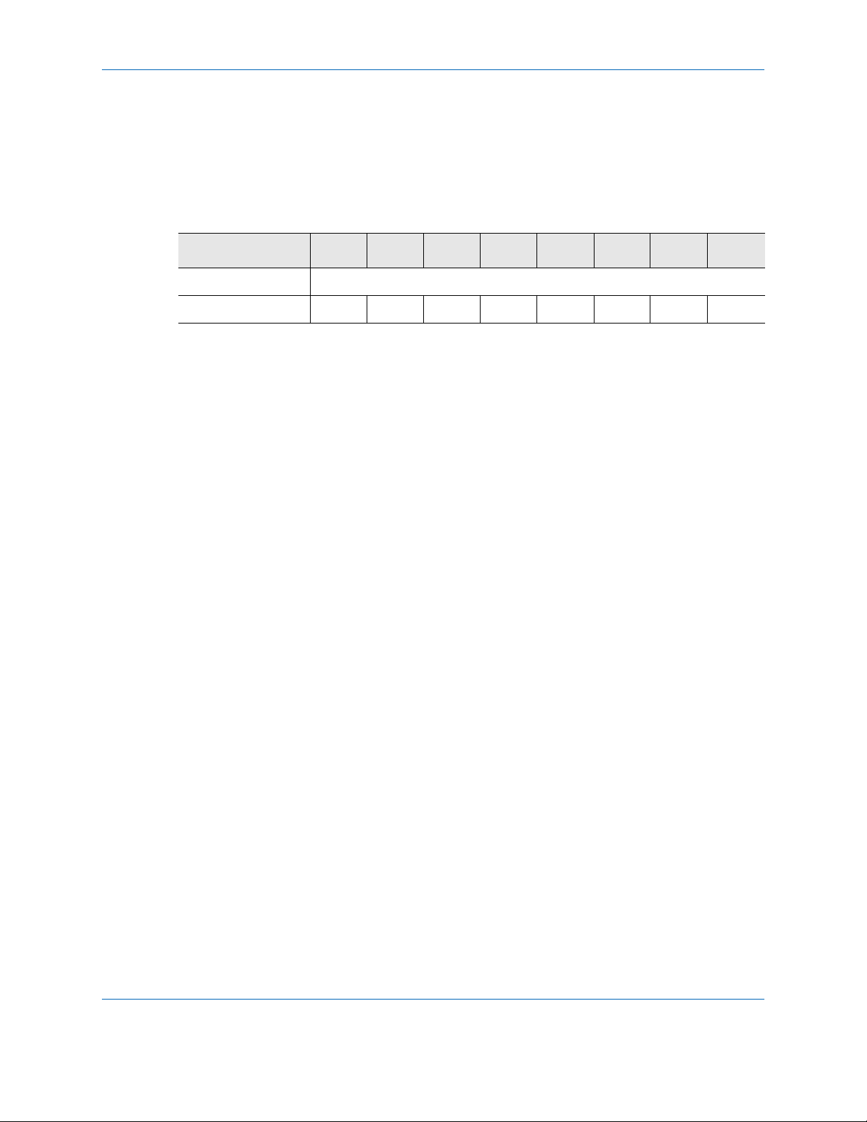
ATA REGISTERS SSD-PXXX(I)-3521 DATA SHEET
SECTOR COUNT REGISTER
The Sector Count register is used to read or write the sector count of the data
for which an ATA transfer has been made.
Table 36: Sector Count Register
Operation
D
7
D
6
D
5
D
4
D
3
D
2
D
1
D
0
Read/Write Sector Count
Default Value 00000001
SILICONSYSTEMS PROPRIETARY
This document and the information contained within it is confidential and proprietary to SiliconSystems, Inc.
3521P-02DSR PAGE 49 FEBRUARY 2, 2009
All unauthorized use and/or reproduction is prohibited.
Page 60
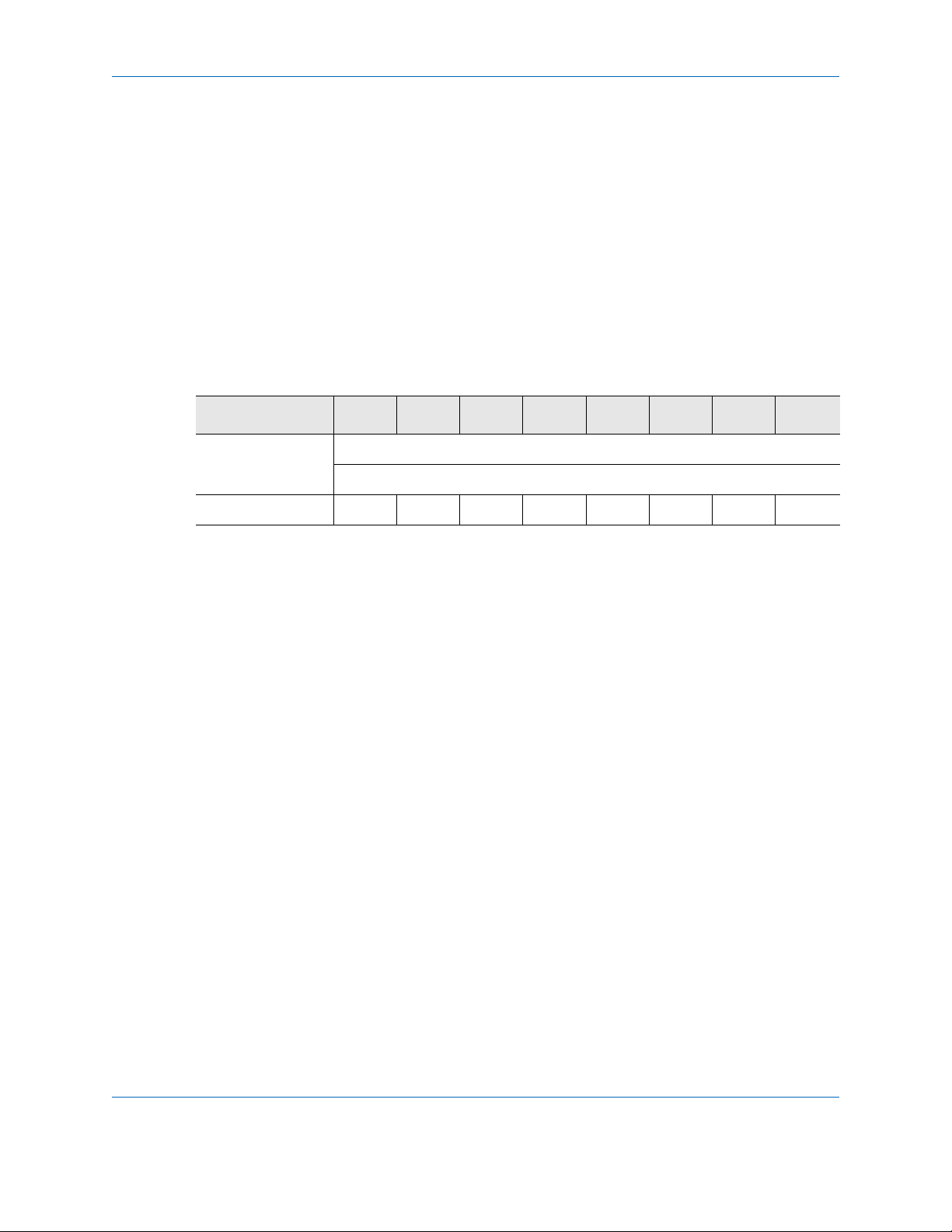
ATA REGISTERS SSD-PXXX(I)-3521 DATA SHEET
SECTOR NUMBER REGISTER
The Sector Number register is set by the host to specify the starting sector
number associated with the next ATA command to be executed. Following a
qualified ATA command sequence, the device sets the register value to the
last sector read or written as a result of the previous AT command.
When Logical Block Addressing (LBA) mode is implemented and the host
issues a command, the contents of the register describe the Logical Block
Number bits A[7:0]. Following an ATA command, the device loads the register
with the LBA block number resulting from the last ATA command.
Table 37: Sector Number Register
Operation
D
7
D
6
D
5
D
4
D
3
D
2
D
1
D
Read/Write Sector Number (CHS Addressing)
Logical Block Number bits A07-A00 (LBA Addressing)
Default Value 0 0 0 0 0 0 0 1
0
SILICONSYSTEMS PROPRIETARY
This document and the information contained within it is confidential and proprietary to SiliconSystems, Inc.
3521P-02DSR PAGE 50 FEBRUARY 2, 2009
All unauthorized use and/or reproduction is prohibited.
Page 61
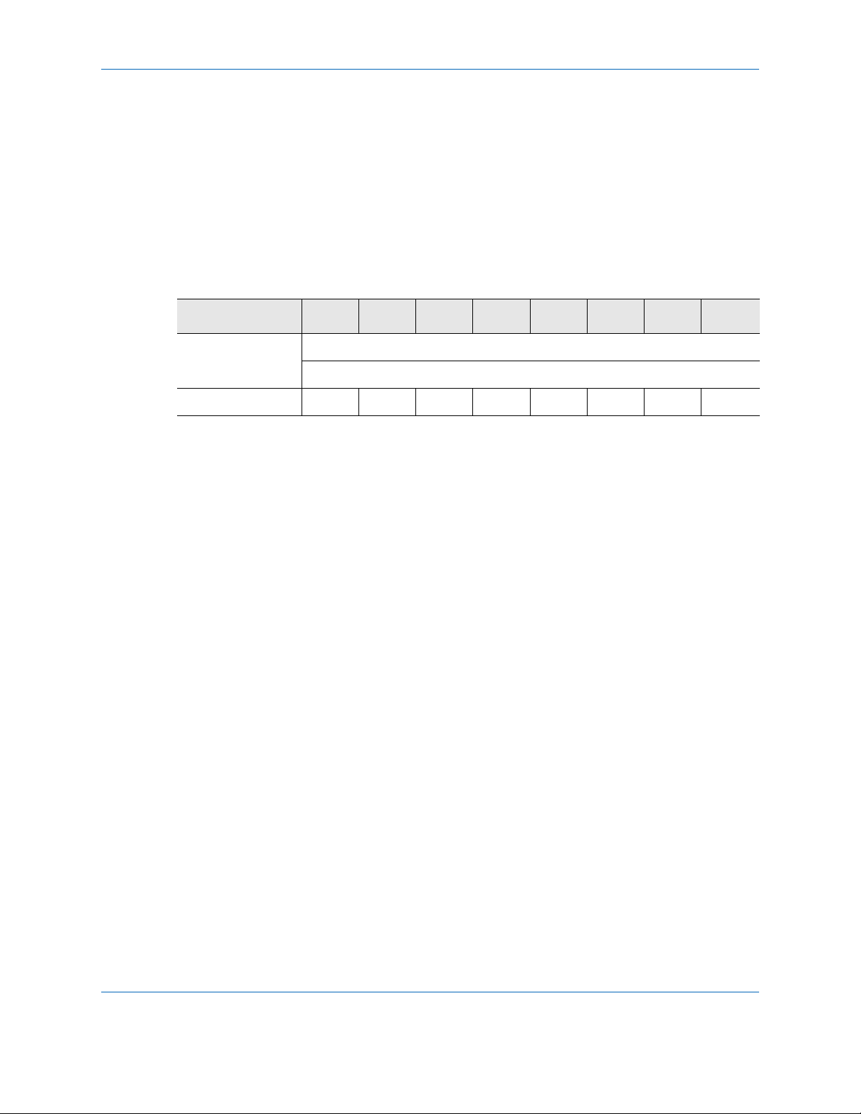
ATA REGISTERS SSD-PXXX(I)-3521 DATA SHEET
CYLINDER LOW REGISTER
The Cylinder Low register is set by the host to specify the cylinder number low
byte. Following an ATA command, the content of the register is written by the
device, identifying the cylinder number low byte.
In LBA mode, the 8-bit register maintains the contents of the Logical Block
number address bits A15:A08.
Table 38: Cylinder Low Register
Operation
D
7
D
6
D
5
D
4
D
3
D
2
D
1
D
Read/Write Cylinder Number Low Byte (CHS Addressing)
Logical Block Number bits A15-A08 (LBA Addressing)
Default Value 0 0 0 0 0 0 0 0
0
SILICONSYSTEMS PROPRIETARY
This document and the information contained within it is confidential and proprietary to SiliconSystems, Inc.
3521P-02DSR PAGE 51 FEBRUARY 2, 2009
All unauthorized use and/or reproduction is prohibited.
Page 62
ATA REGISTERS SSD-PXXX(I)-3521 DATA SHEET
CYLINDER HIGH REGISTER
The Cylinder High register is set by the host to specify the cylinder number
high byte. Following an ATA command, the content of the register is set
internally by the device, identifying the cylinder number high byte.
In LBA mode, the 8-bit register maintains the contents of the Logical Block
number address bits A23:A16.
Table 39: Cylinder High Register
Operation
D
7
D
6
D
5
D
4
D
3
D
2
D
1
D
Read/Write Cylinder Number Low Byte (CHS Addressing)
Logical Block Number bits A23-A16 (LBA Addressing)
Default Value 0 0 0 0 0 0 0 0
0
SILICONSYSTEMS PROPRIETARY
This document and the information contained within it is confidential and proprietary to SiliconSystems, Inc.
3521P-02DSR PAGE 52 FEBRUARY 2, 2009
All unauthorized use and/or reproduction is prohibited.
Page 63

ATA REGISTERS SSD-PXXX(I)-3521 DATA SHEET
DRIVE/HEAD REGISTER
The Drive/Head register is used by the host and the device to select the type
of addressing (CHS or LBA), the drive letter, and either bits 3-0 of the head
number in CHS mode or logical block number bits 27-24 in LBA mode.
Table 40: Drive/Head Register
Operation
Read/Write 1 LBA 1 DRV HS3
Default
D
7
D
6
D
5
D
4
D
3
LBA27
D
2
HS2
LBA26
D
1
HS1
LBA25
D
0
HS0
LBA24
10100000
Value
The Drive/Head register is used by the host to specify one of a pair of ATA
drives present in the platform.
Bit(s) Description
6 LBA. Selects between CHS (0) and LBA (1) addressing mode.
4 Drive Address (DRV). Indicates the drive number selected by the
host, either 0 or 1.
3-0 HS3 to 0. Indicates bits 3-0 of the head number in CHS addressing
mode or LBA bits 27-24 in LBA mode.
• CHS to LBA conversion: LBA = (C x HpC + H) x SpH + S -1
• LBA to CHS conversion:
¶ C = LBA/(HpC x SpH)
¶ H = (LBA/SpH) mod (HpC)
¶ S = (LBA mod(SpH)) + 1
...where:
¶ C is the cylinder number
¶ H is the head number
¶ S is the sector count
¶ HpC is the head count per cylinder count
¶ SpH is the sector count per head count (track)
SILICONSYSTEMS PROPRIETARY
This document and the information contained within it is confidential and proprietary to SiliconSystems, Inc.
3521P-02DSR PAGE 53 FEBRUARY 2, 2009
All unauthorized use and/or reproduction is prohibited.
Page 64
ATA REGISTERS SSD-PXXX(I)-3521 DATA SHEET
STATUS REGISTER
The Status register provides the device’s current status to the host. The status
register is an 8-bit read-only register. When the contents of the register are
read by the host, the IREQ# bit is cleared.
Table 41: Status Register
Operation
D
7
D
6
D
5
D
4
D
3
D
2
D
D
1
0
Read/Write BSY DRDY DWF DSC DRQ CORR IDX ERR
Default Value 0 0 0 0 0 0 0 0
Bit(s) Description
7 Busy (BSY). Set when the drive is busy and unable to process any
new ATA commands.
6 Data Ready (DRDY). Set when the device is ready to accept ATA
commands from the host.
5 Drive Write Fault (DWF). Always set to 0.
4 Drive Seek Complete (DSC). Set when the drive heads have been
positioned over a specific track.
3 Data Request (DRQ). Set when a device is ready to transfer a word
or byte of data to or from the host and the device.
2 Corrected Data (CORR). Always set to 0.
1 Index (IDX). Always set to 0.
0 Error (ERR). Set when an error occurs during the previous ATA
command.
SILICONSYSTEMS PROPRIETARY
This document and the information contained within it is confidential and proprietary to SiliconSystems, Inc.
3521P-02DSR PAGE 54 FEBRUARY 2, 2009
All unauthorized use and/or reproduction is prohibited.
Page 65

ATA REGISTERS SSD-PXXX(I)-3521 DATA SHEET
COMMAND REGISTER
The Command register specifies the ATA command code being issued to the
drive by the host. Execution of the command begins immediately following the
issuance of the command register code by the host.
Table 42: Command Register
Operation
D
7
D
6
D
5
D
4
D
3
D
2
D
1
D
0
Read/Write ATA Command Code
See "ATA Command Block and Set Description" on page 59 for a listing of the
supported ATA commands.
SILICONSYSTEMS PROPRIETARY
This document and the information contained within it is confidential and proprietary to SiliconSystems, Inc.
3521P-02DSR PAGE 55 FEBRUARY 2, 2009
All unauthorized use and/or reproduction is prohibited.
Page 66

ATA REGISTERS SSD-PXXX(I)-3521 DATA SHEET
ALTERNATE STATUS REGISTER
The Alternate Status register is a read-only register indicating the status of the
device, following the previous ATA command. See "Status Register" on page
54 for specific details.
Table 43: Alternate Status Register
Operation
D
7
D
6
D
5
D
4
D
3
D
2
D
D
1
0
Read/Write BSY DRDY DWF DSC DRQ CORR IDX ERR
Default Value 0 0 0 0 0 0 0 0
SILICONSYSTEMS PROPRIETARY
This document and the information contained within it is confidential and proprietary to SiliconSystems, Inc.
3521P-02DSR PAGE 56 FEBRUARY 2, 2009
All unauthorized use and/or reproduction is prohibited.
Page 67
ATA REGISTERS SSD-PXXX(I)-3521 DATA SHEET
DEVICE CONTROL REGISTER
The Device Control register is used to control the interrupt request and issue
ATA software resets.
Table 44: Device Control Register
Operation
D
7
D
6
D
5
D
4
D
3
D
2
D
1
D
0
Write ----1SRSTnIEN0
Bit(s) Description
7-4 Reserved bits.
3 Always set to 1.
2 Software Reset (SRST). When set, resets the ATA software.
1 Interrupt Enable (nIEN). When set, device interrupts are disabled.
There is no function in the memory-mapped mode.
0 Always set to 0.
SILICONSYSTEMS PROPRIETARY
This document and the information contained within it is confidential and proprietary to SiliconSystems, Inc.
3521P-02DSR PAGE 57 FEBRUARY 2, 2009
All unauthorized use and/or reproduction is prohibited.
Page 68
ATA REGISTERS SSD-PXXX(I)-3521 DATA SHEET
DEVICE ADDRESS REGISTER
The Device Address register is used to maintain compatibility with ATA disk
drive interfaces.
Table 45: Device Address Register
Operation
D
7
D
6
D
5
D
4
D
3
D
2
D
1
D
0
Read/Write - nWTG nHS3 nHS2 nHS1 nHS0 nDS1 nDS0
Default Value00 111110
Bit(s) Description
7 Reserved bit.
6 Write Gate (nWTG). Low when a write to the device is in process.
5-2 nHS3 to nHS0. The negated binary address of the currently selected
head.
1 nDS1. Low when drive 1 is selected and active.
0 nDS0. Low when drive 0 is selected and active.
SILICONSYSTEMS PROPRIETARY
This document and the information contained within it is confidential and proprietary to SiliconSystems, Inc.
3521P-02DSR PAGE 58 FEBRUARY 2, 2009
All unauthorized use and/or reproduction is prohibited.
Page 69
ATA COMMAND BLOCK AND SET DESCRIPTION SSD-PXXX(I)-3521 DATA SHEET
ATA COMMAND BLOCK AND SET DESCRIPTION
In accordance with the ANSI ATA Specification, the device implements seven
registers that are used to transfer instructions to the device by the host. These
commands follow the ANSI standard ATA protocol. A description of the ATA
command block is provided in the following table.
Table 46: ATA Command Block and Set Description
Operation
Feature
Sector Count
Sector Number
Cylinder Low
Cylinder High
Drive Head
Command
ATA COMMAND SET
Class Command Name
1 Check Power Mode 98h, E5h - - - - D -
1 Execute Drive
Diagnostics
D
7
1LBA1Drive X
D
6
D
5
D
4
D
3
X
X
X
X
X
X
D
2
D
Table 47: ATA Command Set
Command
Code
FR SC SN CY DH LBA
Registers Used
90h ----D-
1
D
0
1 Erase Sector C0h - YYYYY
2 Format Track 50h - Y - Y Y Y
1 Identify Drive ECh - - - - D -
1 Idle 97h, E3h - Y - - D -
1 Idle Immediate 95h, E1h - - - D -
1 Initialize Drive
91h - Y - - Y -
Parameters
1 Read Buffer E4h - - - - D -
1 Read DMA* C8h - YYYYY
1 Read Multiple C4h - Y Y Y Y Y
SILICONSYSTEMS PROPRIETARY
This document and the information contained within it is confidential and proprietary to SiliconSystems, Inc.
3521P-02DSR PAGE 59 FEBRUARY 2, 2009
All unauthorized use and/or reproduction is prohibited.
Page 70

ATA COMMAND BLOCK AND SET DESCRIPTION SSD-PXXX(I)-3521 DATA SHEET
Table 47: ATA Command Set (Continued)
Registers Used
Class Command Name
Command
Code
FR SC SN CY DH LBA
1 Read Long Sector 22h, 23h - - Y Y Y Y
1 Read Sector(s) 20h, 21h - - Y Y Y Y
1 Read Verify Sector(s) 40h, 41h - Y Y Y Y Y
1 Recalibrate 1Xh - - - - Y -
1 Request Sense 03h - - - - D -
1 Seek 7Xh - - YYYY
1 Set Features EFh Y - - D -
1 Set Multiple Mode C6h - Y - - D -
1 Set Sleep Mode 99h, E6h - - - - D -
1 Standby 96h, E2h - - - - D -
1 Standby Immediate 94h, E0h - - - - D -
1 Translate Sector 87h - YYYYY
1 Wear Level F5h - - - - Y -
2 Write Buffer E8h - - - - D -
1 Write DMA* CAh - YYYYY
2 Write Long Sector 32h, 33h - Y Y Y Y
3 Write Multiple C5h - Y Y Y Y Y
3 Write Multiple w/o
CDh - YYYYY
Erase
2 Write Sector(s) 30h, 31h- YYYYY
2 Write Sector(s) w/o
38h - YYYYY
Erase
3 Write Verify 3Ch - YYYYY
* = This function does not apply to SiliconDrives that have DMA disabled.
Notes:
• CY = Cylinder
• SC = Sector Count
• DH = Drive/Head
• SN = Sector Number
• FR = Feature LBA — LBA bit of the Drive/Head register (D denotes that
only the drive bit is used)
SILICONSYSTEMS PROPRIETARY
This document and the information contained within it is confidential and proprietary to SiliconSystems, Inc.
3521P-02DSR PAGE 60 FEBRUARY 2, 2009
All unauthorized use and/or reproduction is prohibited.
Page 71
ATA COMMAND BLOCK AND SET DESCRIPTION SSD-PXXX(I)-3521 DATA SHEET
Check Power Mode — 98h, E5h
The Check Power Mode command verifies the device’s current power mode.
When the device is configured for standby mode or is entering or exiting
standby, the BSY bit is set, the Sector Count register set to 00h, and the BSY
bit is cleared. In idle mode, BSY is set and the Sector Count register is set to
FFh. The BSY bit is then cleared and an interrupt is issued.
Table 48: Check Power Mode — 98h, E5h
Register
D
7
D
6
D
5
D
4
D
Feature X
Sector Count X
Sector Number X
Cylinder Low X
Cylinder High X
Drive Head X X X Drive
Command 98h or E5h
3
D
2
D
D
1
0
SILICONSYSTEMS PROPRIETARY
This document and the information contained within it is confidential and proprietary to SiliconSystems, Inc.
3521P-02DSR PAGE 61 FEBRUARY 2, 2009
All unauthorized use and/or reproduction is prohibited.
Page 72
ATA COMMAND BLOCK AND SET DESCRIPTION SSD-PXXX(I)-3521 DATA SHEET
Executive Drive Diagnostic — 90h
The Executive Drive Diagnostic performs an internal read write diagnostic test
using (AA55h and 55AAh). If an error is detected in the read/write buffer, the
Error register reports the appropriate diagnostic code.
Table 49: Executive Drive Diagnostic — 90h
Register
D
7
D
6
D
5
D
4
D
3
D
2
Feature X
Sector Count X
Sector Number X
Cylinder Low X
Cylinder High X
Drive Head X X X Drive
Command 90h
D
D
1
0
SILICONSYSTEMS PROPRIETARY
This document and the information contained within it is confidential and proprietary to SiliconSystems, Inc.
3521P-02DSR PAGE 62 FEBRUARY 2, 2009
All unauthorized use and/or reproduction is prohibited.
Page 73
ATA COMMAND BLOCK AND SET DESCRIPTION SSD-PXXX(I)-3521 DATA SHEET
Format Track — 50h
The Format Track command formats the common solid-state memory array.
Table 50: Format Track — 50h
Register
D
7
D
6
D
5
D
4
D
3
D
2
D
D
1
0
Feature X
Sector Count Sector Count
Sector Number Sector Number (LBA7-0)
Cylinder Low Cylinder Low (LBA15-8)
Cylinder High Cylinder High (LBA23-16)
Drive Head 1 LBA 1 Drive Head Number (LBA27-24)
Command 50h
SILICONSYSTEMS PROPRIETARY
This document and the information contained within it is confidential and proprietary to SiliconSystems, Inc.
3521P-02DSR PAGE 63 FEBRUARY 2, 2009
All unauthorized use and/or reproduction is prohibited.
Page 74
ATA COMMAND BLOCK AND SET DESCRIPTION SSD-PXXX(I)-3521 DATA SHEET
Identify Drive — ECh
Issued by the host, the Identify Drive command provides 256 bytes of drive
attribute data (i.e., sector size, count, and so on) The identify drive data
structure is detailed in the following table.
Table 51: Identify Drive — ECh
Register
D
7
D
6
D
5
D
4
D
3
D
2
Feature X
Sector Count X
Sector Number X
Cylinder Low X
Cylinder High X
Drive Head X X X Drive X
Command ECh
D
D
1
0
SILICONSYSTEMS PROPRIETARY
This document and the information contained within it is confidential and proprietary to SiliconSystems, Inc.
3521P-02DSR PAGE 64 FEBRUARY 2, 2009
All unauthorized use and/or reproduction is prohibited.
Page 75

ATA COMMAND BLOCK AND SET DESCRIPTION SSD-PXXX(I)-3521 DATA SHEET
Identify Drive — Drive Attribute Data
Table 52: Identify Drive — Drive Attribute Data
Word
Address
Data Default Bytes Da ta Description
0044Ah (fixed
ID bit) in IDE
mode
2 General configuration bit information
• 15: Non-magnetic disk
• 14: Formatting speed latency
permissible gap needed
• 13: Track Offset option supported
• 12: Data Strobe Offset option supported
• 11: Over 0.5% rotational speed
difference
• 10: Disk transfer rate >10Mbps
• 9: 10Mbps >= disk transfer rate >5Mbps
• 8: 5Mbps >= disk transfer rate
• 7: Removable cartridge drive
• 6: Fixed drive
• 5: Spindle Motor Control option
executed
• 4: Over 15μs changing head time
• 3: Non-MFM encoding
• 2: Soft sector allocation
• 1: Hard sector allocation
•0: Reserved
1 XXXXh 2 Number of cylinders
2 0000h 2 Reserved
3 00XXh 2 Number of heads
4 0000h 2 Number of unformatted bytes per track
5 XXXXh 2 Number of unformatted bytes per sector
6 XXXXh 2 Number of sectors per track
7-8 XXXXh 4 Number of sectors per device
9 0000h 2 Reserved
10-19 XXXXh 20 Serial number
SILICONSYSTEMS PROPRIETARY
This document and the information contained within it is confidential and proprietary to SiliconSystems, Inc.
3521P-02DSR PAGE 65 FEBRUARY 2, 2009
All unauthorized use and/or reproduction is prohibited.
Page 76

ATA COMMAND BLOCK AND SET DESCRIPTION SSD-PXXX(I)-3521 DATA SHEET
Table 52: Identify Drive — Drive Attribute Data (Continued)
Word
Address
Data Default Bytes Da ta Description
20 0002h 2 Buffer type
• 0000h: Not specified
• 0001h: A single-ported, single-sector
buffer
• 0002h: A dual-ported multisector buffer
• 0003h: A dual-ported multisector buffer
with a read caching
21 0002h 2 Buffer size in 512-byte increments
22 0004h 2 Number of ECC bytes passed on read/
write long commands
23-26 XXXXh 8 Firmware revision (eight ASCII characters)
27-46 XXXXh 40 Model number (40 ASCII characters)
47 0001h 2 7-0: Maximum number of sectors that can
be transferred with a Read/Write Multiple
command per interrupt
48 0000h 2 Double word (32 bit) not supported
49 0002h 2 • 11: IORDY supported
• 9: LBA supported
• 8: DMA supported
50 0000h 2 Reserved
51 0100h 2 15-8: PIO data transfer cycle timing
52 0000h 2 15-8: DMA data transfer cycle timing
53 0000h 2 • 1: Words 64-70 are valid
• 0: Words 54-58 are valid
54 XXXXh 2 Current number of cylinders
55 XXXXh 2 Current number of heads
56 XXXXh 2 Current sectors per track
57-58 XXXXh 4 Current capacity in sectors
59 010Xh 2 7-0: Current sectors can be transferred
with a Read/Write Multiple command per
interrupt
60-61 XXXXh 4 Total number of sectors addressable in
LBA mode
62 0000h 2 Single-word DMA modes supported
SILICONSYSTEMS PROPRIETARY
This document and the information contained within it is confidential and proprietary to SiliconSystems, Inc.
All unauthorized use and/or reproduction is prohibited.
3521P-02DSR PAGE 66 FEBRUARY 2, 2009
Page 77

ATA COMMAND BLOCK AND SET DESCRIPTION SSD-PXXX(I)-3521 DATA SHEET
Table 52: Identify Drive — Drive Attribute Data (Continued)
Word
Address
Data Default Bytes Da ta Description
63 0407h 2 Multiword DMA modes supported
64 0003h 2 PIO modes supported
65 0078h 2 Minimum DMA transfer cycle time per
word (ns)
66 0078h 2 Manufacturer’s recommended DMA
transfer cycle time (ns)
67 0078h 2 Minimum PIO transfer cycle time without
flow control (ns)
68 0078h 2 Minimum PIO transfer cycle time with
IORDY flow controls (ns)
69-127 0000h 118 Reserved
128-159 0000h 64 Vendor-unique
160-255 0000h 192 Reserved
SILICONSYSTEMS PROPRIETARY
This document and the information contained within it is confidential and proprietary to SiliconSystems, Inc.
3521P-02DSR PAGE 67 FEBRUARY 2, 2009
All unauthorized use and/or reproduction is prohibited.
Page 78
ATA COMMAND BLOCK AND SET DESCRIPTION SSD-PXXX(I)-3521 DATA SHEET
Idle — 97h, E3h
When issued by the host, the device’s internal controller sets the BSY bit,
enters the Idle mode, clears the BSY bit, and generates an interrupt. If the
sector count is non-zero, it is interpreted as a timer count with each count
being 5ms, and the automatic power-down mode is enabled. If the sector
count is zero, the automatic power-down mode is disabled.
Table 53: Idle — 97h, E3h
Register
D
7
D
6
D
5
D
4
D
3
D
2
Feature X
Sector Count Timer Count (5ms increments)
Sector Number X
Cylinder Low X
Cylinder High X
Drive Head X X X Drive X
Command 97h or E3h
D
D
1
0
SILICONSYSTEMS PROPRIETARY
This document and the information contained within it is confidential and proprietary to SiliconSystems, Inc.
3521P-02DSR PAGE 68 FEBRUARY 2, 2009
All unauthorized use and/or reproduction is prohibited.
Page 79
ATA COMMAND BLOCK AND SET DESCRIPTION SSD-PXXX(I)-3521 DATA SHEET
Idle Immed iate — 95h, E1h
When issued by the host, the device’s internal controller sets the BSY bit,
enters Idle Mode, clears the BSY bit, and issues an interrupt. The interrupt is
issued whether or not the Idle mode is fully entered.
Table 54: Idle Immediate — 95h, E1h
Register
D
7
D
6
D
5
D
4
D
3
D
2
Feature X
Sector Count X
Sector Number X
Cylinder Low X
Cylinder High X
Drive Head X X X Drive X
Command 95h or E1h
D
D
1
0
SILICONSYSTEMS PROPRIETARY
This document and the information contained within it is confidential and proprietary to SiliconSystems, Inc.
3521P-02DSR PAGE 69 FEBRUARY 2, 2009
All unauthorized use and/or reproduction is prohibited.
Page 80
ATA COMMAND BLOCK AND SET DESCRIPTION SSD-PXXX(I)-3521 DATA SHEET
Initialize Drive Parameters — 91h
Initialize Drive Parameters allows the host to set the sector counts per track
and the head counts per cylinder to 1 Fixed. Upon issuance of the command,
the device sets the BSY bit and associated parameters, clears the BSY bit,
and issues an interrupt.
Table 55: Initialize Drive Parameters — 91h
Register
D
7
D
6
D
5
D
4
D
3
D
2
D
1
Feature X
Sector Count Sector Count (Number of Sectors)
Sector Number X
Cylinder Low X
Cylinder High X
Drive Head X 0 X Drive Head Number
(Number of Heads — 1)
Command 91h
D
0
SILICONSYSTEMS PROPRIETARY
This document and the information contained within it is confidential and proprietary to SiliconSystems, Inc.
3521P-02DSR PAGE 70 FEBRUARY 2, 2009
All unauthorized use and/or reproduction is prohibited.
Page 81
ATA COMMAND BLOCK AND SET DESCRIPTION SSD-PXXX(I)-3521 DATA SHEET
Recalibrate — 1Xh
The Recalibrate command sets the cylinder low and high, head number to 0h,
and sector number to 1h in CHS mode. In LBA mode (i.e., LBA = 1), the sector
number is set to 0h.
Table 56: Recalibrate — 1Xh
Register
D
7
D
6
D
5
D
4
D
3
D
2
Feature X
Sector Count X
Sector Number X
Cylinder Low X
Cylinder High X
Drive Head 1 LBA 1 Drive X
Command 1Xh
D
D
1
0
SILICONSYSTEMS PROPRIETARY
This document and the information contained within it is confidential and proprietary to SiliconSystems, Inc.
3521P-02DSR PAGE 71 FEBRUARY 2, 2009
All unauthorized use and/or reproduction is prohibited.
Page 82
ATA COMMAND BLOCK AND SET DESCRIPTION SSD-PXXX(I)-3521 DATA SHEET
Read Buffer — E4h
The Read Buffer command allows the host to read the contents of the sector
buffer. When issued, the device sets the BSY bit and sets up the sector buffer
data in preparation for the read operation. When the data is ready, the DRQ bit
is set and the BSY bit in the Status register are set and cleared, respectively.
Table 57: Read Buffer — E4h
Register
D
7
D
6
D
5
D
4
D
3
D
2
Feature X
Sector Count X
Sector Number X
Cylinder Low X
Cylinder High X
Drive Head X X X Drive X
Command E4h
D
D
1
0
SILICONSYSTEMS PROPRIETARY
This document and the information contained within it is confidential and proprietary to SiliconSystems, Inc.
3521P-02DSR PAGE 72 FEBRUARY 2, 2009
All unauthorized use and/or reproduction is prohibited.
Page 83
ATA COMMAND BLOCK AND SET DESCRIPTION SSD-PXXX(I)-3521 DATA SHEET
Read DMA — C8h
The Read DMA command allows the host to read data using the DMA transfer
protocol.
Note: This function does not apply to SiliconDrives that have DMA
disabled.
Table 58: Read DMA — C8h
Register
D
7
D
6
D
5
D
4
D
3
D
2
D
D
1
0
Feature X
Sector Count Sector Count
Sector Number Sector Number (LBA7-0)
Cylinder Low Cylinder Low (LBA15-8)
Cylinder High Cylinder High (LBA23-16)
Drive Head 1 LBA 1 Drive Head Number (LBA27-24)
Command C8h
SILICONSYSTEMS PROPRIETARY
This document and the information contained within it is confidential and proprietary to SiliconSystems, Inc.
3521P-02DSR PAGE 73 FEBRUARY 2, 2009
All unauthorized use and/or reproduction is prohibited.
Page 84
ATA COMMAND BLOCK AND SET DESCRIPTION SSD-PXXX(I)-3521 DATA SHEET
Read Multiple — C4h
The Read Multiple command executes similarly to the Read Sector command,
with the exception that interrupts are issued only when a block containing the
counts of sectors defined by the Set Multiple command is transferred.
Table 59: Read Multiple — C4h
Register
D
7
D
6
D
5
D
4
D
3
D
2
D
D
1
0
Feature X
Sector Count Sector Count
Sector Number Sector Number (LBA7-0)
Cylinder Low Cylinder Low (LBA15-8)
Cylinder High Cylinder High (LBA23-16)
Drive Head 1 LBA 1 Drive Head Number (LBA27-24)
Command C4h
SILICONSYSTEMS PROPRIETARY
This document and the information contained within it is confidential and proprietary to SiliconSystems, Inc.
3521P-02DSR PAGE 74 FEBRUARY 2, 2009
All unauthorized use and/or reproduction is prohibited.
Page 85
ATA COMMAND BLOCK AND SET DESCRIPTION SSD-PXXX(I)-3521 DATA SHEET
Read Sector — 20 h, 21h
The Read Sector command allows the host to read sectors 1 to 256 as
specified in the Sector Count register. If the sector count is set to 0h, all 256
sectors of data are made available. When the command code is issued and
the first sector of data has been transferred to the buffer, the DRQ bit is set.
The Read Sector command is terminated by writing the cylinder, head, and
sector number of the last sector read in the task file. On error, the read
operation is aborted in the errant sector.
Table 60: Read Sector — 20h, 21h
Register
D
7
D
6
D
5
D
4
D
3
D
2
D
D
1
0
Feature X
Sector Count Sector Count
Sector Number Sector Number (LBA7-0)
Cylinder Low Cylinder Low (LBA15-8)
Cylinder High Cylinder High (LBA23-16)
Drive Head 1 LBA 1 Drive Head Number (LBA27-24)
Command 20h or 21h
SILICONSYSTEMS PROPRIETARY
This document and the information contained within it is confidential and proprietary to SiliconSystems, Inc.
3521P-02DSR PAGE 75 FEBRUARY 2, 2009
All unauthorized use and/or reproduction is prohibited.
Page 86
ATA COMMAND BLOCK AND SET DESCRIPTION SSD-PXXX(I)-3521 DATA SHEET
Read Long Sector(s) — 22h, 23h
The Read Long Sector(s) command operates similarly to the Read Sector(s)
command, with the exception that it transfers requested data sectors and ECC
data. The long instruction ECC byte transfer for Long commands is a byte
transfer at a fixed length of 4 bytes.
Table 61: Read Long Sector(s) — 22h, 23h
Register
D
7
D
6
D
5
D
4
D
3
D
2
D
D
1
0
Feature X
Sector Count X
Sector Number Sector Number (LBA7-0)
Cylinder Low Cylinder Low (LBA15-8)
Cylinder High Cylinder High (LBA23-16)
Drive Head 1 LBA 1 Drive Head Number (LBA27-24)
Command 22h or 23h
SILICONSYSTEMS PROPRIETARY
This document and the information contained within it is confidential and proprietary to SiliconSystems, Inc.
3521P-02DSR PAGE 76 FEBRUARY 2, 2009
All unauthorized use and/or reproduction is prohibited.
Page 87
ATA COMMAND BLOCK AND SET DESCRIPTION SSD-PXXX(I)-3521 DATA SHEET
Read Verify Sector(s) — 40h, 41h
The Read Verify Sector(s) command operates similarly to the Read Sector(s)
command, with the exception that is does not set the DRQ bit and does not
transfer data to the host. When the requested sectors are verified, the onboard
controller clears the BSY bit and issues an interrupt.
Table 62: Read Verify Sector(s) — 40h, 41h
Register
D
7
D
6
D
5
D
4
D
3
D
2
D
D
1
Feature X
Sector Count Sector Count
Sector Number Sector Number (LBA7-0)
Cylinder Low Cylinder Low (LBA15-8)
Cylinder High Cylinder High (LBA23-16)
Drive Head 1 LBA 1 Drive Head Number (LBA27-24)
Command 40h or 41h
0
SILICONSYSTEMS PROPRIETARY
This document and the information contained within it is confidential and proprietary to SiliconSystems, Inc.
3521P-02DSR PAGE 77 FEBRUARY 2, 2009
All unauthorized use and/or reproduction is prohibited.
Page 88
ATA COMMAND BLOCK AND SET DESCRIPTION SSD-PXXX(I)-3521 DATA SHEET
Seek — 7Xh
The Seek command seeks and picks up the head to the tracks specified in the
task file. When the command is issued, the solid-state memory chips do not
need to be formatted. After an appropriate amount of time, the DSC bit is set.
Table 63: Seek — 7Xh
Register
D
7
D
6
D
5
D
4
D
3
D
2
D
D
1
0
Feature X
Sector Count X
Sector Number Sector Number (LBA7-0)
Cylinder Low Cylinder Low (LBA15-8)
Cylinder High Cylinder High (LBA23-16)
Drive Head 1 LBA 1 Drive Head Number (LBA27-24)
Command 7Xh
SILICONSYSTEMS PROPRIETARY
This document and the information contained within it is confidential and proprietary to SiliconSystems, Inc.
3521P-02DSR PAGE 78 FEBRUARY 2, 2009
All unauthorized use and/or reproduction is prohibited.
Page 89
ATA COMMAND BLOCK AND SET DESCRIPTION SSD-PXXX(I)-3521 DATA SHEET
Set Features — EFh
The Set Features command allows the host to configure the feature set of the
device according to the attributes listed in Table 65.
Table 64: Set Features — EFh
Register
D
7
D
6
D
5
D
4
D
3
D
2
Feature Feature
Sector Count X
Sector Number X
Cylinder Low X
Cylinder High X
Drive Head X X X Drive X
Command EFh
Table 65: Set Features’ Attributes
Feature Operation
01h Enable 8-bit data transfer
66h Disable reverting to power on defaults
81h Disable 8-bit data transfer
BBh 4 bytes of data apply on Read/Write Long commands
CCh Enable revert to power on defaults
D
D
1
0
On power-up or following a hardware reset, the device is set to the default
mode 81h.
SILICONSYSTEMS PROPRIETARY
This document and the information contained within it is confidential and proprietary to SiliconSystems, Inc.
3521P-02DSR PAGE 79 FEBRUARY 2, 2009
All unauthorized use and/or reproduction is prohibited.
Page 90
ATA COMMAND BLOCK AND SET DESCRIPTION SSD-PXXX(I)-3521 DATA SHEET
Set Multiple Mode — C6h
The Set Multiple Mode command allows the host to access the drive via Read
Multiple and Write Multiple ATA commands. Additionally, the command sets
the block count (i.e., the number of sectors within the block) for the Read/Write
Multiple command. The sector count per block is set in the Sector Count
register.
Table 66: Set Multiple Mode — C6h
Register
D
7
D
6
D
5
D
4
D
3
D
2
Feature X
Sector Count Sector Count
Sector Number X
Cylinder Low X
Cylinder High X
Drive Head X X X Drive X
Command C6h
D
D
1
0
SILICONSYSTEMS PROPRIETARY
This document and the information contained within it is confidential and proprietary to SiliconSystems, Inc.
3521P-02DSR PAGE 80 FEBRUARY 2, 2009
All unauthorized use and/or reproduction is prohibited.
Page 91
ATA COMMAND BLOCK AND SET DESCRIPTION SSD-PXXX(I)-3521 DATA SHEET
Set Sleep Mode — 99h, E6h
The Set Sleep Mode command allows the host to set the device in sleep
mode. When the onboard controller transitions to sleep mode, it clears the
BSY bit and issues an interrupt. The device interface then becomes inactive.
Sleep mode can be exited by issuing either a hardware or software reset.
Table 67: Set Sleep Mode — 99h, E6h
Register
D
7
D
6
D
5
D
4
D
3
D
2
Feature X
Sector Count X
Sector Number X
Cylinder Low X
Cylinder High X
Drive Head X X X Drive X
Command 99h or E6h
D
D
1
0
SILICONSYSTEMS PROPRIETARY
This document and the information contained within it is confidential and proprietary to SiliconSystems, Inc.
3521P-02DSR PAGE 81 FEBRUARY 2, 2009
All unauthorized use and/or reproduction is prohibited.
Page 92
ATA COMMAND BLOCK AND SET DESCRIPTION SSD-PXXX(I)-3521 DATA SHEET
Standby — 96h, E2h
When the Standby command is issued by the host, it transitions the device into
standby mode. If the Sector Count register is set to a value other than 0h, the
Auto Powerdown function is enabled and the device returns to Idle mode.
Table 68: Standby — 96h, E2h
Register
D
7
D
6
D
5
D
4
D
3
D
2
Feature X
Sector Count Timer Count (5ms x Timer Count)
Sector Number X
Cylinder Low X
Cylinder High X
Drive Head X X X Drive X
Command 96h or E2h
D
D
1
0
SILICONSYSTEMS PROPRIETARY
This document and the information contained within it is confidential and proprietary to SiliconSystems, Inc.
3521P-02DSR PAGE 82 FEBRUARY 2, 2009
All unauthorized use and/or reproduction is prohibited.
Page 93
ATA COMMAND BLOCK AND SET DESCRIPTION SSD-PXXX(I)-3521 DATA SHEET
Standby Immediate — 94h, E0h
When the Standby Immediate command is issued by the host, it transitions the
device into standby mode.
Table 69: Standby Immediate — 94h, E0h
Register
D
7
D
6
D
5
D
4
D
3
D
2
Feature X
Sector Count X
Sector Number X
Cylinder Low X
Cylinder High X
Drive Head X X X Drive X
Command 94h or E0h
D
D
1
7
SILICONSYSTEMS PROPRIETARY
This document and the information contained within it is confidential and proprietary to SiliconSystems, Inc.
3521P-02DSR PAGE 83 FEBRUARY 2, 2009
All unauthorized use and/or reproduction is prohibited.
Page 94
ATA COMMAND BLOCK AND SET DESCRIPTION SSD-PXXX(I)-3521 DATA SHEET
Write Buffer — E8h
The Write Buffer command allows the host to rewrite the contents of the
512- byte data buffer with the wanted data.
Table 70: W rit e Buffer — E8h
Register
D
7
D
6
D
5
D
4
D
3
D
2
Feature X
Sector Count X
Sector Number X
Cylinder Low X
Cylinder High X
Drive Head X X X Drive X
Command E8h
D
D
1
7
SILICONSYSTEMS PROPRIETARY
This document and the information contained within it is confidential and proprietary to SiliconSystems, Inc.
3521P-02DSR PAGE 84 FEBRUARY 2, 2009
All unauthorized use and/or reproduction is prohibited.
Page 95
ATA COMMAND BLOCK AND SET DESCRIPTION SSD-PXXX(I)-3521 DATA SHEET
Write DMA — CAh
The Write DMA command allows the host to write data using the DMA transfer
protocol.
Note: This function does not apply to SiliconDrives that have DMA
disabled.
Table 71: Write DMA — CAh
Register
D
7
D
6
D
5
D
4
D
3
D
2
D
D
1
Feature X
Sector Count Sector Count
Sector Number Sector Number (LBA7-0)
Cylinder Low Cylinder Low(LBA15-8)
Cylinder High Cylinder High(LBA23-16)
Drive Head X LBA X Drive Head Number(LBA27-24)
Command CAh
0
SILICONSYSTEMS PROPRIETARY
This document and the information contained within it is confidential and proprietary to SiliconSystems, Inc.
3521P-02DSR PAGE 85 FEBRUARY 2, 2009
All unauthorized use and/or reproduction is prohibited.
Page 96
ATA COMMAND BLOCK AND SET DESCRIPTION SSD-PXXX(I)-3521 DATA SHEET
Write Multiple — C5h
The Write Multiple command operates in the same manner as the Write Sector
command. When issued, the device sets the BSY bit within 400ns and
generates an interrupt at the completion of a transferred block of sectors. The
DRQ bit is set at the beginning of a block transfer.
Table 72: Write Multiple — C5h
Register
D
7
D
6
D
5
D
4
D
3
D
2
D
D
1
Feature X
Sector Count Sector Count
Sector Number Sector Number (LBA7-0)
Cylinder Low Cylinder Low(LBA15-8)
Cylinder High Cylinder High(LBA23-16)
Drive Head X LBA X Drive Head Number(LBA27-24)
Command C5h
0
SILICONSYSTEMS PROPRIETARY
This document and the information contained within it is confidential and proprietary to SiliconSystems, Inc.
3521P-02DSR PAGE 86 FEBRUARY 2, 2009
All unauthorized use and/or reproduction is prohibited.
Page 97
ATA COMMAND BLOCK AND SET DESCRIPTION SSD-PXXX(I)-3521 DATA SHEET
Write Sector(s) — 30h, 31h
The Write Sector(s) command writes from 1 to 256 sectors as specified in the
Sector Count register. A sector count of 0 requests 256 sectors. When issued,
the device sets the BSY bit within 400ns and generates an interrupt at the
completion of a transferred block of sectors. The DRQ bit is set at the
beginning of a block transfer.
Table 73: Write Sector(s) — 30h, 31h
Register
D
7
D
6
D
5
D
4
D
3
D
2
D
D
1
0
Feature X
Sector Count Sector Count
Sector Number Sector Number (LBA7-0)
Cylinder Low Cylinder Low (LBA15-8)
Cylinder High Cylinder High (LBA23-16)
Drive Head X LBA X Drive Head Number (LBA27-24)
Command 30h or 31h
SILICONSYSTEMS PROPRIETARY
This document and the information contained within it is confidential and proprietary to SiliconSystems, Inc.
3521P-02DSR PAGE 87 FEBRUARY 2, 2009
All unauthorized use and/or reproduction is prohibited.
Page 98
ATA COMMAND BLOCK AND SET DESCRIPTION SSD-PXXX(I)-3521 DATA SHEET
Write Long Sector(s) — 32h, 33h
The Write Long Sector(s) command operates in the same manner as the Write
Sector command — when issued, the device sets the BSY bit within 400ns
and generates an interrupt at the completion of a transferred block of sectors.
The DRQ bit is set at the beginning of a block transfer.
Table 74: Write Long Sector(s) — 32h, 33h
Register
D
7
D
6
D
5
D
4
D
3
D
2
D
D
1
0
Feature X
Sector Count Sector Count
Sector Number Sector Number (LBA7-0)
Cylinder Low Cylinder Low (LBA15-8)
Cylinder High Cylinder High (LBA23-16)
Drive Head X LBA X Drive Head Number (LBA27-24)
Command 32h or 33h
SILICONSYSTEMS PROPRIETARY
This document and the information contained within it is confidential and proprietary to SiliconSystems, Inc.
3521P-02DSR PAGE 88 FEBRUARY 2, 2009
All unauthorized use and/or reproduction is prohibited.
Page 99
ATA COMMAND BLOCK AND SET DESCRIPTION SSD-PXXX(I)-3521 DATA SHEET
Erase Sector(s) — C0h
The Erase Sector(s) command is issued prior to the issuance of a Write
Sector(s) or Write Multiple w/o Erase command.
Table 75: Erase Sector(s) — C0h
Register
D
7
D
6
D
5
D
4
D
3
D
2
D
D
1
0
Feature X
Sector Count Sector Count
Sector Number Sector Number (LBA7-0)
Cylinder Low Cylinder Low (LBA15-8)
Cylinder High Cylinder High (LBA23-16)
Drive Head X LBA X Drive Head Number (LBA27-24)
Command C0h
SILICONSYSTEMS PROPRIETARY
This document and the information contained within it is confidential and proprietary to SiliconSystems, Inc.
3521P-02DSR PAGE 89 FEBRUARY 2, 2009
All unauthorized use and/or reproduction is prohibited.
Page 100
ATA COMMAND BLOCK AND SET DESCRIPTION SSD-PXXX(I)-3521 DATA SHEET
Request Sense — 03h
The Request Sense command identifies the extended error codes generated
by the preceding ATA command. The Request Sense command must be
issued immediately following the detection of an error via the Error register.
Table 76: Request Sense — 03h
Register
D
7
D
6
D
5
D
4
D
3
D
2
Feature X
Sector Count X
Sector Number X
Cylinder Low X
Cylinder High X
Drive Head 1 X 1 Drive X
Command 03h
The extended error codes are defined in the following table.
Table 77: Extended Error Codes
Extended Error Codes Description
00h No error detected
01h Self test is OK (no error)
09h Miscellaneous error
20h Invalid command
D
D
1
0
21h Invalid address (requested head or sector invalid)
2Fh Address overflow (address too large)
35h, 36h Supply or generated voltage out of tolerance
11h Uncorrectable ECC error
18h Corrected ECC error
05h, 30h-32h, 37h,3Eh Self test of diagnostic failed
10h, 14h ID not found
3Ah Spare sectors exhausted
1Fh Data transfer error/aborted command
0Ch, 38h, 3Bh, 3Ch, 3Fh Computed media format
03h Write/erase failed
SILICONSYSTEMS PROPRIETARY
This document and the information contained within it is confidential and proprietary to SiliconSystems, Inc.
3521P-02DSR PAGE 90 FEBRUARY 2, 2009
All unauthorized use and/or reproduction is prohibited.
 Loading...