

Page 1
SiI 141B PanelLink
®
Digital Receiver
General Description
The SiI 141B uses PanelLink Digital technology to support displays
ranging from VGA to High Ref resh XGA (25-86 MHz), which is ideal for LCD
desktop monit or appl i cations. W i t h a flexible single or dual pixel out interface
and selectable out put drive, the SiI 141B receiver supports up to true color
panels (24 bit/pixel, 16.7M colors) in 1 pixel/clock mode (18 bit/pixel in 2
pixel/clock mode). P anelLink also f eatures an int er-pair s kew tolerance up to
1 full input clock c ycle. The SiI 141B is pin for pin compatible with the SiI
141 but incorporates a number of enhancements. These include an
improved jitter tolerant PLL design, new HSYNC fi lter and power down when
the clock is inactive. All PanelLink products are designed on a scaleable
CMOS architecture to support future performance requirements while
maintaining the sam e logical interface. System designers can be assured
that the interface will be fixed through a number of technology and
performance generations.
PanelLink Digital technology si mplifies PC design by resolving m any of
the system level is sues associated with high-s peed digital design, providing
the system designer with a digital interf ace solution t hat is quic ker to mark et
and lower in cost.
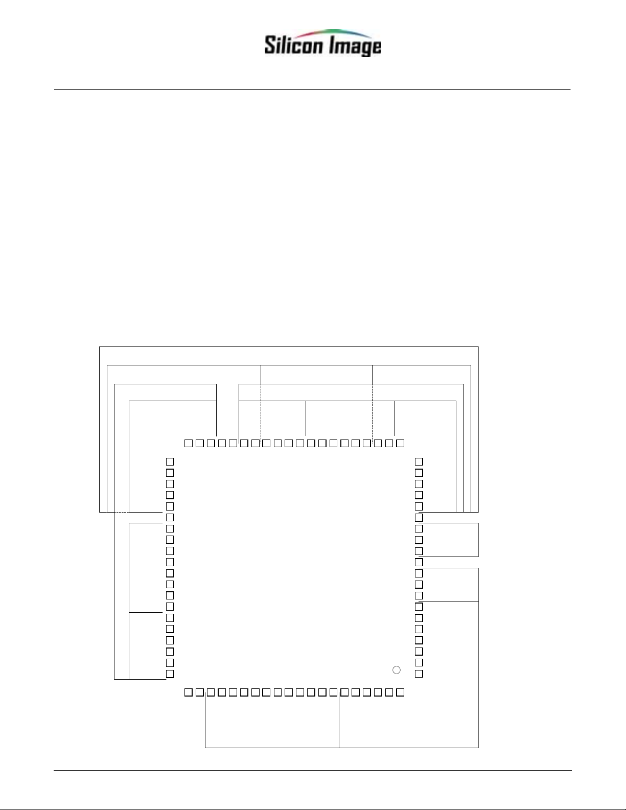
SiI 141B Pin Diagram
24-bit Input Data for 1-pixel/clock mode
8-bit Channel 2 Data
1-pixel/clock
6-bit Odd Channel 0
Data 2-pixel/clock
6-bit Even Channel 2
Data 2-pixel/clock
8-bit Channel 1 Data
1-pixel/clock
18-bit Even Data for 2-pixel/clock mode
6-bit Even Channel 1
Data 2-pixel/clock
May 2001
Features
• Scaleable Bandwidth: 25-86 MHz (VGA to High
• Low Power: 3.3V core operation & power-down mode
• Automatic power down when clock is inactive
• High Skew Tolerance: 1 full input cl ock cycle (15ns at
• Pin-compatible with Si I 101, SiI 141
• Sync Detect: for Plug & Display “Hot Plugging”
• Cable Distance Support: over 5m with twisted-pair,
• Compliant with DVI 1.0 (DVI is backwards compat i bl e
Refresh XGA)
65 MHz)
fiber-optics ready
with VESA® P&D
8-bit Channel 0 Data
1-pixel/clock
TM
and DFP)
ODCK36
GND
Q18
VCC
Q19
37
38
39
DE
Q20
Q21
Q22
Q23 45
OGND
Q24
OVCC
Q25
VCC
Q26
Q27
18-bit Odd Data for 2-pixel/clock mode
Data 2-pixel/clock
6-bit Odd Channel 1
Q28
Q29
Q30
Q31
Q32
Q33
Q34
Data 2-pixel/clock
6-bit Odd Channel 2
Q35
40
41
42
43
44
46
47
48
49
50
51
52
53
54
55
56
57
58
59
60
62
61
63
64
VCC
GND
AVCC
RX2+
RX2- 65
DIFFERENTIAL SIGNAL
Q15
Q16
Q17
33
34
35
SiI141B
80-Pin TQFP
(Top View)
68
66
67
RX1-
RX1+
AGND
Q14
32
69
AVCC
Q13
31
RX0+ 70
Q12
30
71
RX0-
Q11
29
72
AGND
OVCC
28
73
RXC-
Q10
27
74
RXC+
HSYNC_DEJTR 75
77
76
PVCC
EXT_RES
78
PGND
Q521
Q622Q723Q824Q925OGND26
Q4
20
Q3
19
Q218
Q1
17
16
15
14
12
11
10
9
7
6
5
4
2
1
79
ST
OCK_INV 80
Data 2-pixel/clock
6-bit Even Channel 0
Q0
OVCC
VSYNC
OGND13
HSYNC
GND
CTL3
CTL2
CTL18
SCDT
DFO
PIXS
OGND
PDO3
PD
RESERVED
MISC.
CONTROL
PURPOSE
GENERAL
CONTROL
Subject to Change without Notice
Page 2
SiI 141B SiI-DS-0037-C
]
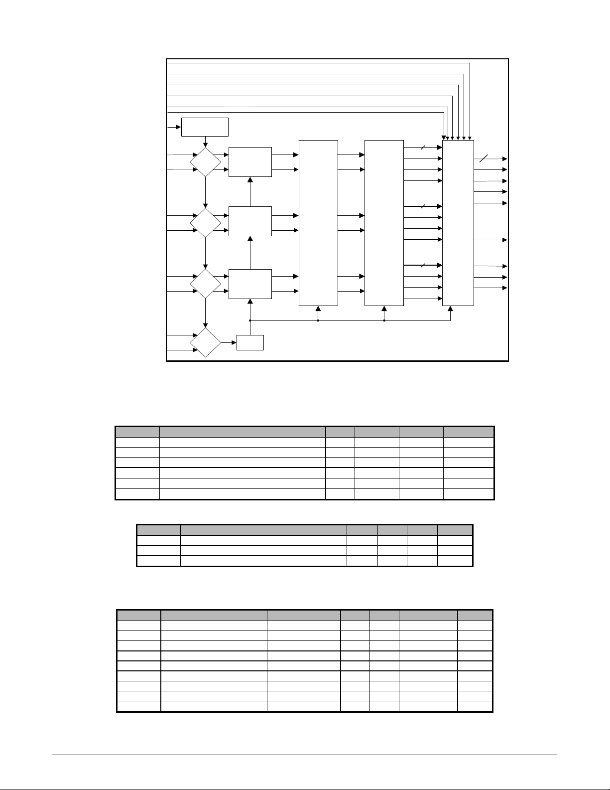
Functional Block Diagram
ST
PIXS
DFO
OCK_INV
PDO
HSYNC_DEJTR
EXT_RES
RX2+
RX2-
RX1+
RX1-
Termination
Control
VCR
VCR
DATA
RECOVERY
CH2
DATA
RECOVERY
CH1
INTER-
CHANNEL
SYNC.
DECODER
8
CLT3
CLT2
DE2
8
CLT1
PLL_SYNC
DE1
PANEL
INTER-
FACE
LOGIC
24/36
Q[35:0/23:0
ODCK
DE
HSYNC
VSYNC
SCDT
RX0+
RX0-
RXC+
RXC-
Absolute Maximum Conditions
Normal Operating Conditions
DC Digital I/O Specifications
Note: Permanent device damage may occur if absolute maximum conditions are exceeded.
Functional operation should be rest ri cted to the conditions des cribed under Normal Operating Conditions .
Symbol Parameter Min Typ Max Units
VCC Supply Voltage 3.3V -0.3 4.0 V
VI Input Voltage -0.3 VCC+ 0.3 V
VO Output Voltage -0.3 VCC+ 0.3 V
TA Ambient Temperature (with power applied) -25 105
T
Storage Temperature -65 150
STG
θ
Thermal Resistance (J unction to Ambient) 45
JA
Symbol Parameter Min Typ Max Units
VCC Supply Voltage 3.0 3.3 3.6 V
V
Supply Voltage Noise 100 mV
CCN
TA Ambient Temperature (with power applied) 0 25 70
Under normal operating conditions unl ess otherwise specified.
Symbol Parameter Conditions Min Typ Max Units
VIH High-level Input Voltage 2 V
VIL Low-level Input Voltage 0.8 V
VOH High-level Output Voltage 2.4 V
VOL Low-level Output Volt age 0.4 V
V
Input Cl amp Voltage1 I
CINL
V
I nput Clamp Voltage1 I
CIPL
V
Output Clamp Voltage1 I
CONL
V
Output Clamp Voltage1 I
COPL
IIL Input Leakage Current -10 10
Note: 1 Guaranteed by design. Voltage undershoot or overshoot cannot exceed absolute maxim um conditions
for a pulse of greater than 3 ns or one third of the clock cycle.
VCR
VCR
DATA
RECOVERY
CH0
PLL
8
VSYNC
HSYNC
DE0
°C /W
P-P
°C
= -18mA GND -0.8 V
CL
= 18mA IVCC + 0.8 V
CL
= -18mA GND -0.8 V
CL
= 18mA OVCC + 0.8 V
CL
CLT1
CLT2
CLT3
°C
°C
µA
Silicon Image, Inc. 2 Subject to Change without Notice
Page 3
SiI 141B SiI-DS-0037-C
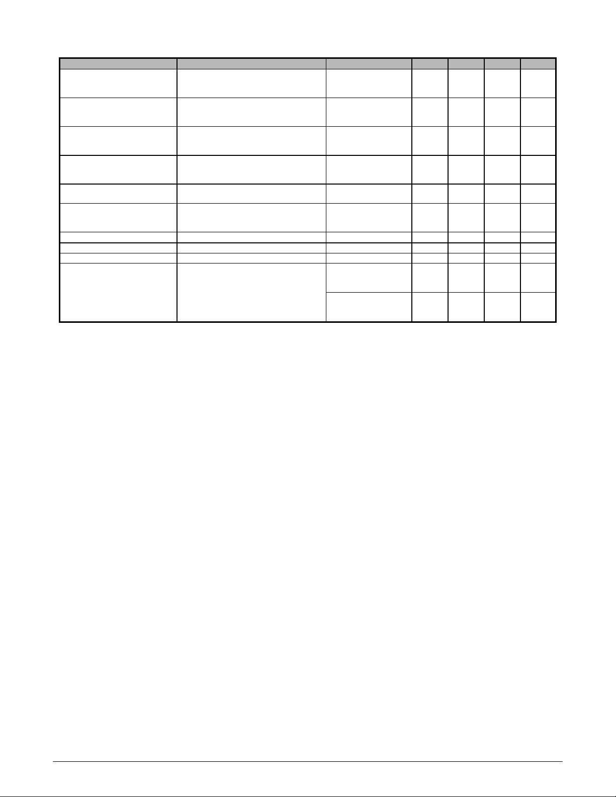
DC Specifications
Under normal operating conditions unl ess otherwise specified. Low drive st rength values, when ST=0, are shown in brackets.
Symbol Parameter Conditions Min Typ Max Units
I
Output High Drive
OHD
Data and Controls
I
Output Low Drive
OLD
Data and Controls
I
ODCK High Drive V
OHC
I
ODCK Low Drive V
OLC
VID Differential Input Voltage
Single Ended Amplitude
I
Output leakage current to ground in
PDL
high impedance mode (PD, P DO =
LOW)
IPD Power-down Current1 50 100
I
Power-down Current RXC± Inactive 4 7 mA
CLKI
I
Power-down-output Current 125 155 mA
PDO
I
Receiver Supply Current
CCR
ODCK=86MHz, 1-pixel/clock mode
Notes:
2
3
4
1
The transmitter must be in power-down mode, powered off, or disconnect ed for the current to be under this maximum.
For worst case I/O power consumption.
The Typical Pattern contains a gray scale area, checkerboard area, and text.
Black and white checkerboard pattern, each c hecker is one pixel wide.
V
OUT
ST=1
ST=0
V
OUT
ST=1
ST=0
OUT
ST=1
ST=0
OUT
ST=1
ST=0
= 2.4
= 0.4
= 2.4
= 2.0
5.0
2.5
-5.5
-2.8
10.1
5.0
-11.1
-5.5
10.3
5.2
-8.3
-4.2
20.6
10.3
-16.7
-8.3
17.6
8.8
-11.2
-5.6
35.1
17.6
-22.4
-11.2
mA
mA
mA
mA
75 1000 mV
10
µA
µA
C
LOAD
2
R
EXT_SWING
Typical Pattern
C
LOAD
R
EXT_SWING
Worst Case Pattern
= 10pF
= 10pF
= 510 Ω
3
= 510 Ω
4
157
172
182
194
mA
mA
Silicon Image, Inc. 3 Subject to Change without Notice
Page 4
SiI 141B SiI-DS-0037-C
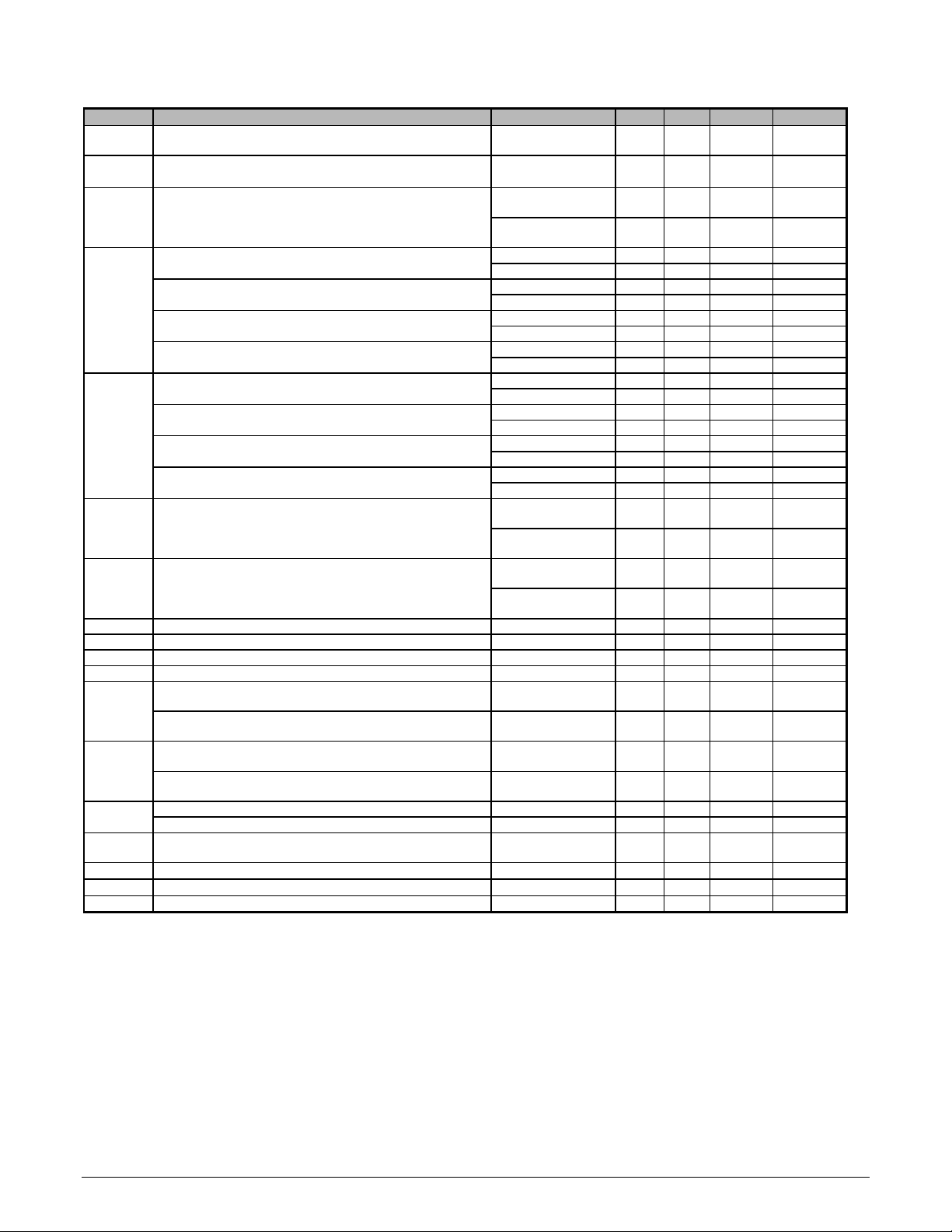
AC Specifications
Under normal operating conditions unl ess otherwise specified. Low drive strength values, when ST=0, are given below.
Symbol Parameter Conditions Min Typ Max Units
T
Intra-Pair (+ to -) Differential Input Sk ew 86 MHz
DPS
T
Channel to Channel Differenti al Input Skew 86 MHz
CCS
T
Worst Case Di fferential Input Clock Jitter tolerance
IJIT
1,2
D
LHT
(43 MHz, 2-pixel/clock, PIXS=1)
65 MHz
86 MHz
CL = 10pF; ST = 1 3.5 ns Low-to-High Transition Time: Data and Cont rol s
= 5pF; ST = 0 4.5 ns
C
L
CL = 10pF; ST = 1 3.5 ns Low-to-High Transition Time: Data and Cont rol s
(65 MHz, 1-pixel/clock, PIXS=0)
= 5pF; ST = 0 4.5 ns
C
L
CL = 10pF; ST = 1 1.6 ns Low-to-High Transition Time: ODCK
(43 MHz, 2-pixel/clock, PIXS=1)
Low-to-High Transition Time: ODCK
(65 MHz, 1-pixel/clock, PIXS=0)
D
C
High-to-Low Transition Time: Data and Cont rol s
HLT
(43 MHz, 2-pixel/clock, PIXS=1)
C
High-to-Low Transition Time: Data and Cont rol s
(65 MHz, 1-pixel/clock, PIXS=0)
C
High-to-Low Transition Time: ODCK
(43 MHz, 1-pixel/clock, PIXS=0)
C
High-to-Low Transition Time: ODCK
(65 MHz, 1-pixel/clock, PIXS=0)
T
SETUP
Data, DE, VSYNC, HSYNC, and CTL[3:1] Setup Tim e t o
C
= 5pF; ST = 0 2.1 ns
C
L
CL = 10pF; ST = 1 1.6 ns
CL = 5pF; ST = 0 2.1 ns
= 10pF; ST = 1 3.0 ns
L
= 5pF; ST = 0 4.2 ns
C
L
= 10pF; ST = 1 3.0 ns
L
= 5pF; ST = 0 4.2 ns
C
L
= 10pF; ST = 1 1.5 ns
L
= 5pF; ST = 0 1.9 ns
C
L
= 10pF; ST = 1 1.5 ns
L
= 5pF; ST = 0 1.9 ns
C
L
= 10pF; ST = 1 3.6
L
ODCK falling edge (OCK_INV = 0) or to ODCK ri sing
edge (OCK_INV = 1)
*OCK_INV = 1
T
HOLD
Data, DE, VSYNC, HSYNC, and CTL[3:1] Hold Time from
C
= 5pF; ST = 0 18.4
C
L
= 10pF; ST = 1 8.0
L
ODCK falling edge, (OCK_INV = 0) or f rom ODCK rising
edge (OCK_INV = 1)
*OCK_INV = 0
R
ODCK Cycle Time (1 pixel/cl ock) 11.6 40 ns
CIP
F
ODCK Frequency (1 pixel/clock) 25 86 MHz
CIP
R
ODCK Cycle Time (2 pixels/clock) 23.3 80 ns
CIP
F
ODCK Frequency (2 pixels/clock) 12.5 43 MHz
CIP
R
ODCK High Time
CIH
65 MHz, One Pixel / Clock, PIXS = 0
3
43 MHz, Two Pixel / Clock, PIXS = 1 3 C
R
ODCK Low Time
CIL
65 MHz, One Pixel / Clock, PIXS = 0
3
43 MHz, Two Pixel / Clock, PIXS = 1 3 C
T
Link disabled (DE inac tive) to SCDT low1 160 ms
HSC
= 5pF; ST = 0 24.0
C
L
C
= 10pF, ST=1
L
= 5pF, ST=0
C
L
= 10pF, ST=1
L
= 5pF, ST=0
C
L
C
= 10pF, ST=1
L
= 5pF, ST=0
C
L
= 10pF, ST=1
L
= 5pF, ST=0
C
L
Link disabled (Tx power down) to SCDT low 5 200 250 ms
T
Link enabl ed (DE active) to SCDT high6
FSC
T
Delay from RXC+/- Inactive to high i mpedance outputs RXC+/- = 25MHz 10
CLKPD
T
Delay from RXC+/- active to data active RXC+/- = 25MHz 100
CLKPU
T
Del ay from PD/ PDO Low to high impedance outputs 8 ns
PDL
Notes: 1 Jitter defined as per DVI 1.0 Specification, Section 4.6 Jitter S pecification.
2
Jitter measured with Clock Recovery Unit as per DVI 1.0 Specifi cation, Section 4.7 E l ectrical Measurement Procedures.
3
Output clock duty c yc l e i s independent of the differential i nput clock duty cycle and the IDCK duty cycle.
4
The setup and hold timing for the data and controls relative to the ODCK rising edge (OCK_INV=1) is by design the same
as the falling edge timing.
5
Measured when transmitter was powered down (see SiI/AN-0005 “PanelLi nk Basic Design /Appl i cation Guide,” Section 2.4).
6
Refer to the transmitter datasheet for mini mum DE high and low time
7
Data is active (i.e. not tri-stated) but not valid yet . Data and controls are valid only when SCDT goes high. See T
Figure 7.
470
7
465
350
3.0*
ns
19.0*
ns
8.4*
ns
24.5*
5.0
4.4
9.0
ns
8.2
6
5
9
ns
9
40
ps
ns
ps
ps
ns
ns
ns
Falling
DE edges
µs
µs
and
FSC
Silicon Image, Inc. 4 Subject to Change without Notice
Page 5
SiI 141B SiI-DS-0037-C
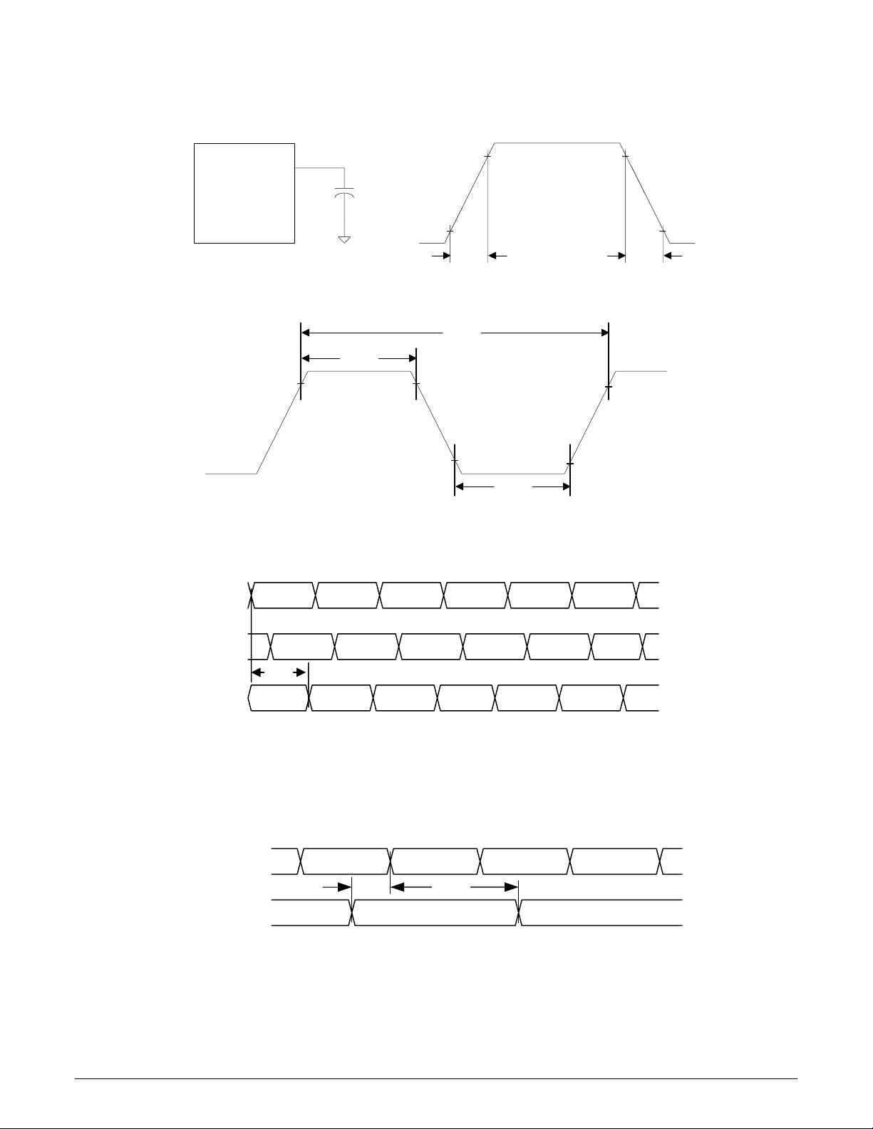
Timing Diagrams
2.0 V 2.0 V
10pF (5pF)SiI141B
0.8 V 0.8 V
D
LHT
D
HLT
Figure 1. Digital Output Transition Times
R
CIP
R
CIH
2.0 V
Figure 2. Receiver Clock Cycle/High/Low Times
2.0 V 2.0 V
0.8 V
R
CIL
0.8 V
RX0
V
= 0V
DIFF
RX1
Output Timing
ODCK_INV = 1
ODCK_INV = 0
QE[23:0]/QO[23:0],
DE, VSYNC, HSYNC,
CTL[3:1]
RX2
V
= 0VT
CCS
DIFF
Figure 3. Channel-to-Channel Skew Timing
T
SETUP
T
HOLD
Figure 4. Output Data Setup/Hold Times to ODCK
Silicon Image, Inc. 5 Subject to Change without Notice
Page 6
SiI 141B SiI-DS-0037-C
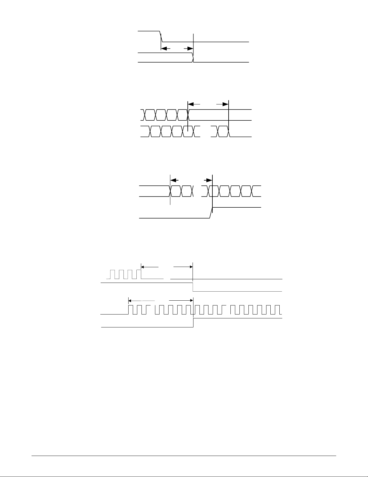
PD
T
Q[35:0], DE,
PDL
VSYNC, HSYNC,
CTL[3:1]
Figure 5. Output Signals Disabled Timing from PD Active
T
CLKPD
RXC
Q[35:0], DE,
VSYNC, HSYNC,
CTL[3:1]
...
...
Figure 6. Output Signals Disabled Timing from Clock Inactive
T
+ T
CLKPU
FSC
...
RXC
...
SCDT
Figure 7. Wake-up on Clock Detect
T
DE
SCDT
DE
SCDT
HSC
T
FSC
Figure 8. SCDT Timing from DE Inactive/Active
Silicon Image, Inc. 6 Subject to Change without Notice
Page 7
SiI 141B SiI-DS-0037-C
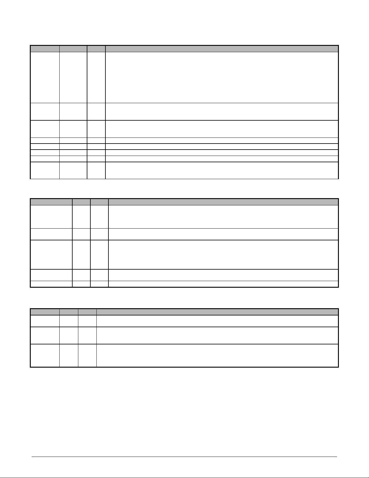
Output Pin Description
Pin Name Pin # Type Description
Q35 – Q0 See Out
Pin
Diagram
ODCK 36 Out
DE 41 Out Output Data Enable.
A low level on PD or PDO will put the output drivers into a high impedance (tri-state) mode. A weak
HSYNC 12 Out Horizontal Sync output control signal.
VSYNC 14 Out Vertical Sync output cont rol signal.
CTL1 8 Out
CTL2 9 Out General output cont rol signal 2
CTL3 10 Out
SiI 141B
Output Data [35:0].
Output data is synchronized with output data clock (ODCK).
When PIXS is low Q35-Q24 are low and Q23-Q0 output 24-bit/ pi xel data.
When PIXS is high Q17-Q0 out put the even numbered pixels (pixel 0, 2, 4, ... , etc.) and Q35-Q18 output
the odd numbered pixels (pixel 1, 3, 5, ... , etc.).
Refer to the TFT Signal Mapping (SiI/AN-0008) and DSTN S i gnal Mapping (S i I/AN-0007) application notes
which tabulate the relationship bet ween the input data to the transmitter and output data from the recei ver.
A low level on PD or PDO will put the output drivers into a high impedance (tri-stat e) mode. A weak
internal pull-down device brings each output to ground.
Output Data Clock.
A low level on PD or PDO will put the output drivers into a high impedance (tri-stat e) mode. A weak
internal pull-down device brings each output to ground.
internal pull-down device brings each output to ground.
General output control signal 1. Thi s pin is not controlled by PDO.
General output control signal 3.
A low level on PD or PDO will put the output drivers into a high impedance (tri-stat e) mode. A weak
internal pull-down device brings each output to ground.
Configuration Pin Description
Pin Name Pin # Type Description
OCK_INV 80 In ODCK Polarity. A low level selects normal ODCK output, which enables data latching on the f alling
PIXS 5 In Pixel Select. A low level indicates that output data is one pixel (up to 24-bit) per clock and a hi gh l evel
DF0 6 In Output Data Format. This pin controls clock and data output format. A low level indicates that ODCK
HSYNC_DEJTR 75 In A low level enables the HSYNC de-jitter circuitry. A high level disables the de-jitter circuit ry. If left
ST 79 In Output Driver Strength. A low level indicat es low drive. A high level indicates hi gh dri ve.
edge. A high level (3.3V) selec t s inverted ODCK output, which enables dat a l atching on the rising edge.
Both conditions are for color TFT panel support. For color 24-bit DSTN panel support, please ref er t o t he
DSTN Signal Mapping (SiI/AN-0008-A) appli cation note.
(3.3V) indicates that output data is two pixels (up to 36-bit) per clock.
runs continuously for color TFT panel support and a high level (3.3V) indic at es that ODCK is stopped
(LOW) for color 24-bit DSTN panel support when DE is low. Refer to the TFT Signal Mapping (SiI/AN-
0007-A) and DSTN Signal Mapping (SiI/AN-0008-A) application notes for a table on TFT or DSTN panel
support.
unconnected, the circui try defaults to disabled.
Power Management Pin Description
Pin Name Pin # Type Description
SCDT 7 Out SyncDetect. A high level is output when DE is toggling. A low level is output when DE is inactive. See page
PD 2 In Power Down (active low). A high level (3.3V) indicates normal operation and a low level indicates power down
PDO 3 In Power Down Output (active low). A high level indicat es normal operation. A low level puts the output drivers
9.
mode. During power down mode all internal circ uitry is powered down and digital I/O are set the s ame as
when PDO is asserted. (see PDO pin description).
only into a high impedance (tri -state) mode. A weak internal pul l -down device bri ngs each output to ground.
There is an internal pull-up resist or on P DO that defaults the chip to normal operation if left unc onnected.
SCDT and CTL1 are not tri-stated by this pi n. See explanation of clock detec t on page 8-9.
Silicon Image, Inc. 7 Subject to Change without Notice
Page 8
SiI 141B SiI-DS-0037-C
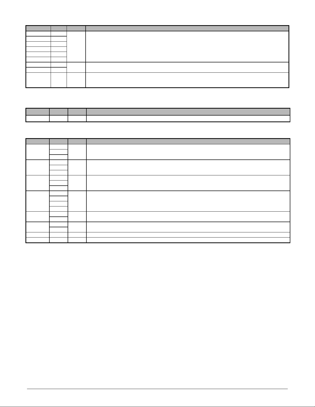
Differential Signal Data Pin Description
Pin Name Pin # Type Description
RX0+ 70 Analog TMDS Low Voltage Differential Si gnal i nput data pairs.
RX0- 71
RX1+ 67
RX1- 68
RX2+ 64
RX2- 65
RXC+ 74 Analog TMDS Low Voltage Different i al Signal input clock pair.
RXC- 73
EXT_RES 76 Analog Impedance Mat ching Control. Resistor value s houl d be ten times the charac t eri stic impedance of the cable.
In the common c ase of 50Ω transmission line, an external 530Ω resi stor must be connect ed between AVCC
and this pin.
Reserved Pin Description
Pin Name Pin # Type Description
RSVD 1 Out This signal must be left unconnect ed.
Power and Ground Pin Description
Pin Name Pin # Type Description
VCC 39 Power Core VCC, m ust be set to 3.3V.
50
61
GND 11 Ground Digital GND.
37
62
OVCC 15 Power Out put VCC, must be set t o 3.3V.
28
48
OGND 4 Ground Output GND.
13
26
46
AVCC 63 Power Analog VCC, m ust be set to 3.3V.
69
AGND 66 Ground Analog GND.
72
PVCC 77 Power PLL VCC, must be set to 3.3V.
PGND 78 Ground PLL GND.
Application Information
The SiI141B is pin for pin com patible with the SiI141 but includes two new features, HSYNC de-jitter and power
down when the clock is inactive.
HSYNC de-jitter enables the 141B to operate properly even when the HSYNC signal contains jitter. Pin 75 is used
to enable or disable this c apability (a reserved pin tied high on the SiI141). T ying this pin low enables the HSYNC
de-jitter circuitry while tying it high disables the circuitry. The HSYNC de-jitter circuitry operates normally with most
VESA standard timings. Som e DOS mode resolutions do not have timings that ar e a multiple of eight (HSYNC
and VSYNC total times and front and back porch times are multiples of eight pixel times). If they are not a multiple
of eight, operation is not guaranteed and the HSYNC de-jitter circuitry should be turned off. When HSYNC dejitter is enabled, the circuitry will introduce anywhere from 0 to 7 CLK delays in the HSYNC signal relative to the
output data.
The SiI141B includes a new power saving feature, power down with clock detect cir cuit. T he SiI141B will go into a
low power mode when there is no video clock coming from the transmitter. In this mode the entire chip is powered
down except the clock detec t c ircuitry. During this m ode digital I/O are s et to a high im pedance (tr i-state) mode. A
weak internal pull-down device brings eac h output to ground. The device power down and wake-up times are
shown in Figures 6 and 7.
The SiI141B also includes a sync detect feature f or pin compatibility with SiI141. In both the SiI141 and SiI141B,
SCDT goes low when DE is inactive.
Silicon Image, Inc. 8 Subject to Change without Notice
Page 9
SiI 141B SiI-DS-0037-C
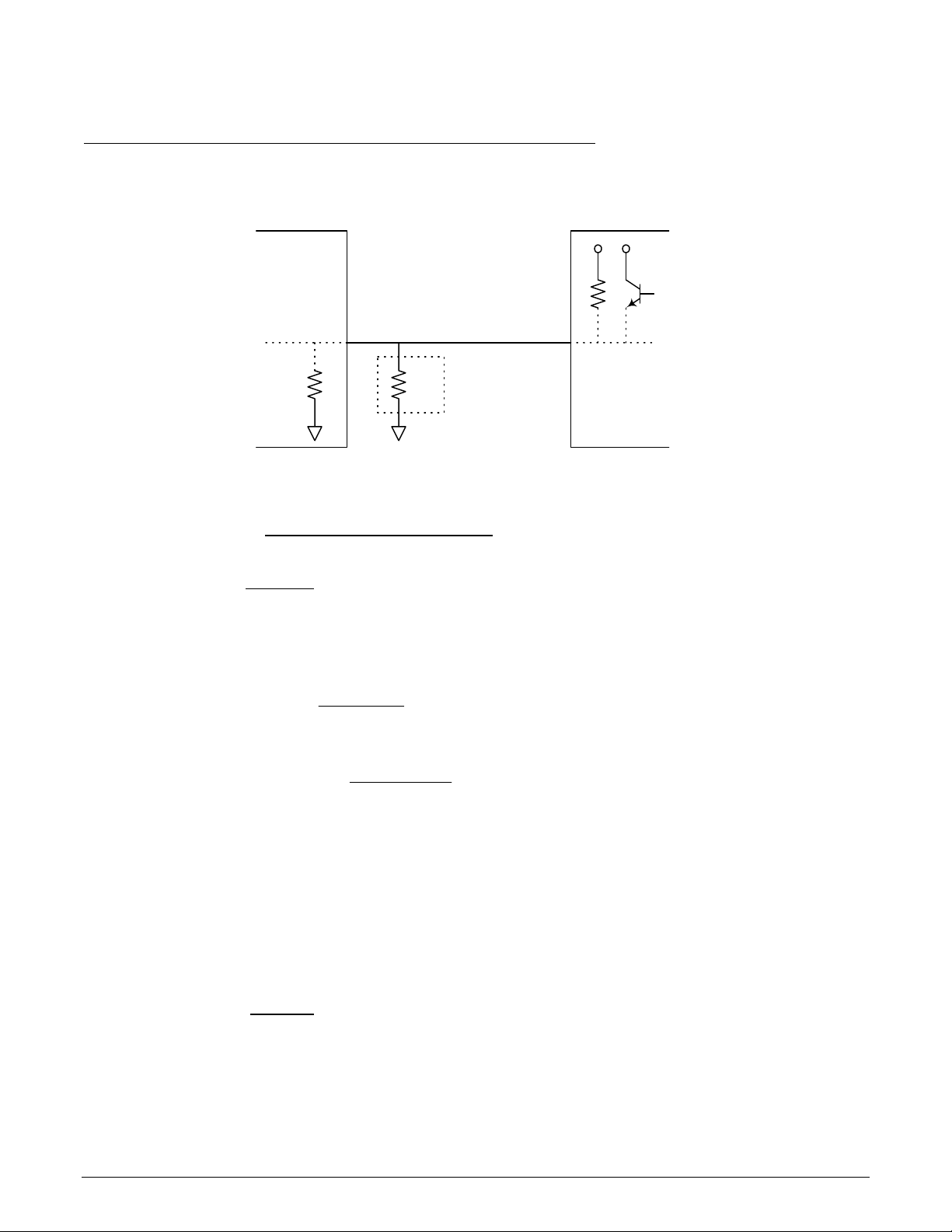
In some application, SCDT is connected to the PDO pin to provide a power savings mode. In others, SCDT is
connected to an external circuit to signal when an incom ing video signal is available. These external devices may
use an internal pull up which can cause problems.
If SCDT is connected to an exter nal circuit which has an internal pull up
video signal is present. The recom mended circuit to k eep SCDT low is shown Figure 9. For most applications,
Silicon Image recom mends a pull down resistor of 1.5 KΩ. However, conditions within every design may vary.
Please use the calculations below to determine the proper pull-down resistor value.
, then SCDT will not stay low when no
SCDT(pin# 7)
weak internal
pull down
SiI141B
Figure 9. Schematic for SCDT connected to external device with pull up
The external pull down resistor value depends on the pull-up circ uit in the external device and can be calculated
with Equation [1] and [2] if the pull up is a passive circuit
manufacture of the other device.
The calculation for the m aximum
power consumption is achieved by mak ing the resistor value as large as possible. Equation [1] determines the
maximum value of R while ensuring that SCDT stays lower than V
impedance. The small current flowing into the SiI141B internal pull down resistor is ignored in equation [1].
Equation [1a]
Equation [1b]
Example :
Pull-up resistor value is 10 KΩ, VIL of external chip is 0.8V, and maximum Vcc is 3.6V
The resistor value should be smaller than 2,857 KΩ.
resistor value is shown in the equation [1] below. In powered down mode, low
R
−
UpPull
()
<
R
()
R < 2,857ohms = (10 KΩ x 0.8V) / (3.6V – 0.8V)
R
pull down resister
RR
+
×
VR
−
−
VV
max
. If the pull up is an active circuit, please c onsult the
of the external chip when SCDT goes into high
IL
VV
<×
ILCCMAX
ILUpPull
ILcc
internal pull up
external
chip
The calculation for the minimum
SCDT voltage exceeds V
the SiI141B internal pull-down resistor is ignored.
Silicon Image, Inc. 9 Subject to Change without Notice
IH
resistor value is shown in the equation [2]. The m inimum value is set so the
of the external chip in norm al operation. In equation [2], the small current flowing into
Page 10

SiI 141B SiI-DS-0037-C
Equation [2]
Example :
When ST(pin# 79) = 1,Vcc = 3.3V
R > 660Ω = Vcc (or V
The resistor value should be larger than 660ohms
When ST(pin# 79) = 0,Vcc = 3.3V
R > 1,320Ω = Vcc (or V
The resistor value should be larger than 1,320ohms.
These examples assume Vcc (or V
smaller.
of external chip) / Min I
IH
of external chip) / Min I
IH
>
R
I
OHDMIN
) of 3.3V, with a lower VIH, the minimum pull down resistor value may be
IH
V
CC
or
= 3.3V / 5.0mA
OHD
OHD
>
R
I
OHDMIN
= 3.3V / 2.5mA
V
IH
Silicon Image, Inc. 10 Subject to Change without Notice
Page 11
SiI 141B SiI-DS-0037-C
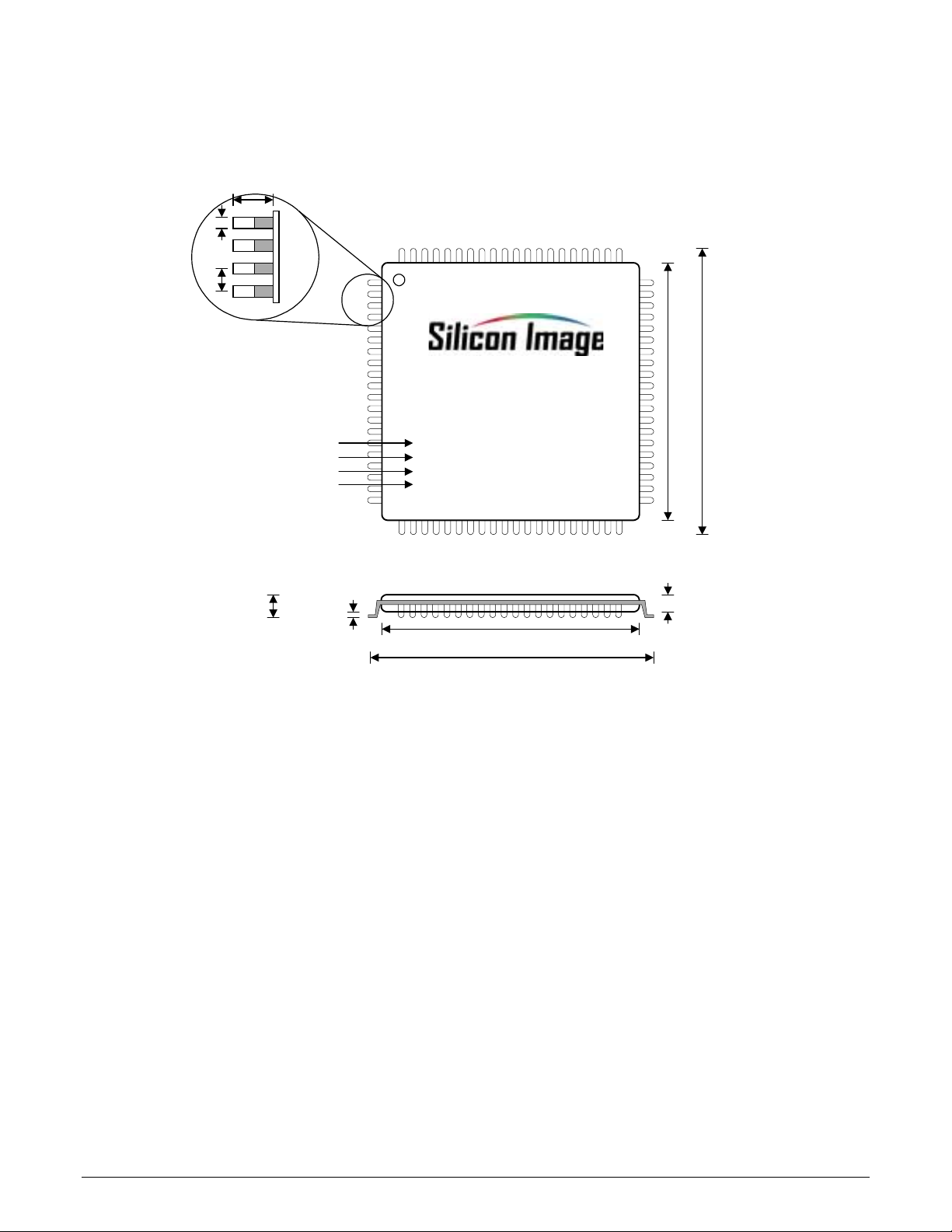
80-pin TQFP Package Dimensions
Lead Length
1.00mm
80-pin Plastic TQFP
Lead Width
0.22mm
Lead Pitch
0.50mm
Body Size 12.00mm
Device #
Lot #
Date Code #
SiI Rev. #
SiI141BCT80
LNNNNN.NLLL
XXYY
X.XX
Footprint 14.00mm
Package Height
1.15mm max.
Clearance
0.15mm max.
Body Size 12.00mm
Footprint 14.00mm
Body Thickness
1.0mm
Silicon Image, Inc. 11 Subject to Change without Notice
Page 12

SiI 141B SiI-DS-0037-C
To obtain the most updated Application Notes and other useful information for your design application, please visit
the Silicon Image web site at
www.siimage.com
, or contact your local Silicon Image sales office.
Copyright Notice
This manual is copyrighted by Silicon Image, Inc. Do not reproduce, transform to any other format, or send/transmit any part o f this
documentation without the express written perm ission of Silicon Image, I nc.
Trademark Acknowledgment
Silicon Image, the Silicon Image logo, PanelLink and the PanelLink Digital logo are t rademarks or registered trademark s of Silicon Image,
Inc. All other trademarks are the property of their respective holders.
Disclaimer
This document provides technic al inf ormation for the user. Silicon Image, Inc. reserves the right t o modify the information in thi s document
as necessary. The customer should make sure that they have the most recent data sheet version. Silicon Image, I nc. holds no responsibility
for any errors that may appear in thi s document. Customers should take appropriate action to ensure their use of t he products does not
infringe upon any patents. Silicon Image, Inc. respects valid patent rights of third parties and does not infringe upon or assist others t o
infringe upon such rights.
Ordering Information
Part Number: SiI141BCT80
Revision History
Revision Date Comment
A 11/00 Full release
B 1/01 Added application information concerning HSYNC de-jitter and power down on clock
C 5/01 Updated EXT_RES value for 50Ω transmission line.
© 2001 Silicon Image, Inc. 5/ 01 SiI-DS-0037-C
Silicon Image, Inc. Tel: 408-616-4000
1060 E. Arques Ave Fax: 408-830-9530
Sunnyvale, CA 94086 E-Mail: [email protected]
USA Web: www.siimage.com
www.panellink.com
Silicon Image, Inc. 12 Subject to Change without Notice
 Loading...