

Silan
Semiconductors
ELECTRONIC VOLUME CONTROLLER
DESCRIPTION
The SC9153A is CMOS IC which has been designed for
electronization volume control of audio equipment,etc.
FEATURES
*Wide operating voltage range(V
*Low current comsumption .
*Attenuation can be controlled from 0dB to –66dB by 2dB/step
*Both of dual power suppliers of (+) and (-) and a single power
supply can be used.
*Be capable of controlling attenuation by means of the built-in
oscillator and the up/down terminals.
6V ~ 12V)
DD=
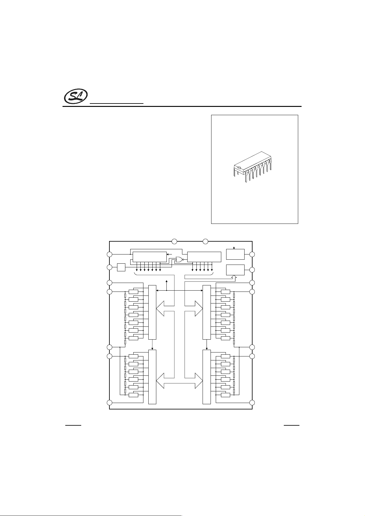
BLOCK DIAGRAM
U/D
10
OSC
9
L-OUT1
2
L-IN1
3
A-GND
4
L-IN2
5
6
OSC
U/D
CK
A-SW
A-SW
A-SW
A-SW
A-SW
A-SW
A-SW
A-SW
A-SW
A-SW
A-SW
A-SW
A-SW
7 Bits Bidirectional
shift registor
VDD VSS
INT
U/D
6 Bits Bidirectional
CK
VDD
CK CK
7 Bits Latch Circuit
6BitsLatchCircuit
116
shift registor
7BitsLatchCircuit
CKCK
6 Bits Latch Circuit
INT
Auto Initialize
A-SW
A-SW
A-SW
A-SW
A-SW
A-SW
A-SW
A-SW
A-SW
A-SW
A-SW
A-SW
A-SW
SC9153A
INH
Circuit
Constant
Current
Circuit
7
DCO
8
R-OUT1
15
R-IN1
14
A-GND
13
R-IN2
12
R-OUT2L-OUT2
11
DIP-16
HANGZHOU SILAN MICROELECTRONICS JOINT-STOCK CO.,LTD
Rev: 1.0 2000.12.31
1
Silan
Semiconductors
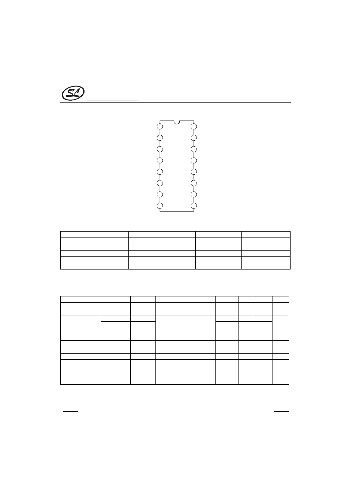
PIN CONFIGURATION
Vss
1
16
VDD
SC9153A
L-OUT1
L-IN1
A-GND
L-IN2
L-OUT2
INH
DCO
2
3
4
SC9153A
5
6
7
8
15
14
13
12
11
10
9
R-OUT1
R-IN1
A-GND
R-IN2
R-OUT2
U/D
OSC
ABSOLUTE MAXIMUM RATINGS
Characteristic Symbol Value Unit
Supply Voltage(Pin 16) V
Input/Output Voltage V
PowerDissipation P
DD
IN
D
Operating Temperature Topr -30 ~ +75
Storage Temperature Tstg -55 ~ +125
13.0 V
Vss-0.3V ~ VDD+0.3V V
150 mW
°C
°C
ELECTRICAL CHARACTERISTICS
(Tamb=25°C,VDD=12.0V, VSS=0V, Unless otherwise specified)
Parameter Symbol Test conditions Min Typ Max Unit
Operating Supply Voltage V
Operating supply current I
Input Voltage
“H” Level V
“L” Level V
Backup current I
Attenuator 1 (10dB/step) resistor R
Attenuator 2 (2dB/step) resistor R
DD
DD
IH
INH,U/D
IL
VDD=4V,INH=”L” 10
B
ATT-1R-IN1(L-IN1
ATT-2R-IN2(L-IN2
)~A-GND 25 50 70
)~A-GND 10 20 28
612V
13mA
0.8*V
DD
Vss-0.3 0.2*V
VDD+0.3
DD
V
µA
kΩ
kΩ
Attenuator Error 2dB
Maximum Input Amplitude Vin Biase VDD/2=6V 4.0 Vrms
Total Harmonic Distortion THD ATT=-10dB, fin=1kHz,
0.005 0.01 %
Vin=1.0Vp-p
DCO output current I
Oscillation frequency f
1 step 70 100 140
DCO
OSC
5 10k Hz
µA
HANGZHOU SILAN MICROELECTRONICS JOINT-STOCK CO.,LTD
Rev: 1.0 2000.12.31
2
Silan
Semiconductors
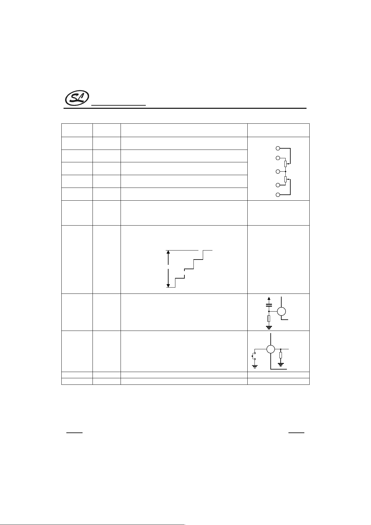
FUNCTIONAL DESCRIPTION OF EACH TERMINAL
Terminal
No.
2,15
3,14
4,13 A-GND
5,12
6,11
7 INH Inhibit terminal. When this terminal is at “L” level, all
8 DCO DC current output for displaying attenuation. Attenuation
Symbol Function Remarks
L-OUT1,
R-OUT1
L-IN1,
R-IN1
L-IN2,
R-IN2
L-OUT2,
R-OUT2
10dB/step attenuator outputs. A signal applied to IN is
attenuated in 7 steps from 0dB to 60dB at 10dB/step.
10dB/step attenuator inputs
Analog ground terminal
2dB/step attenuator inputs
2dB/step attenuator outputs. A signal applied to IN is
attenuated in 5 steps from 0dB to 8dB at 2dB/step.
input/output cut off and the SC9153A is placed in the
inhibit state. When at “H” level, the SC9153A operates
normally.
0dB~∞ is divided into 13 steps and approx 100µA/step is
transmitted.
0dB
1step=100µA
SC9153A
L and R are symmetrical.
Out1
IN1
A-
GND
IN2
Out2
Attenuation can be
converted to DC voltage
by attaching a resistor
between this terminal and
Vss.
13 steps
~
~
∞
9 OSC R,C connecting terminal or the oscillator. Up/down speed
10 U/D Attenuation terminal for oscillator. When this terminal is
1 VSS (-) Power supply terminal
16 VDD (+) Power supply terminal
of attenuation is decided by the attenuation up/down
control oscillator according to this time constant.
at “H” level, sound volume is increased synchronizing
with rise of the oscillator. Conversely, when this pin is at
“L” level, sound volume is decreased.
HANGZHOU SILAN MICROELECTRONICS JOINT-STOCK CO.,LTD
3
VDD
OSC
U/D
Rev: 1.0 2000.12.31
 Loading...