


SC7313S
Silan
Semiconductors
SC7313
HANGZHOU SILAN MICROELECTRONICS JOINT-STOCK CO.,LTD
Rev: 1.1 2002.02.26
1
DIGITAL CONTROLLED STEREO
AUDIO PROCESSOR WITH LOUDNESS
DESCRIPTION
The SC7313 is a volume, tone (bass and treble), balance (left/
right) and fader(front/rear) processor for quality audio applications in
car radio and Hi-Fi systems. Selectable input g
a
in and external
loudness function are provided. Control is accomplished by serial
I
2
C bus microprocessor interface. The AC signal settings is obtained
by resistor networks and switches combined with operational
amplifiers. Due to the Used BIPOLAR/CMOS technology, low
distortion, low noise andlow DC stepping are obtained.
FEATURES
* Input multiplexer:
--3 stereo inputs
--Selectable input gain for optimal adaptation to different
sources
* Four speaker attenuators:
--4 independent speakers control in 1.25dB steps for
balance and fader facilities
--Independent mute function
* All functions programmable via serial I
2
CBus
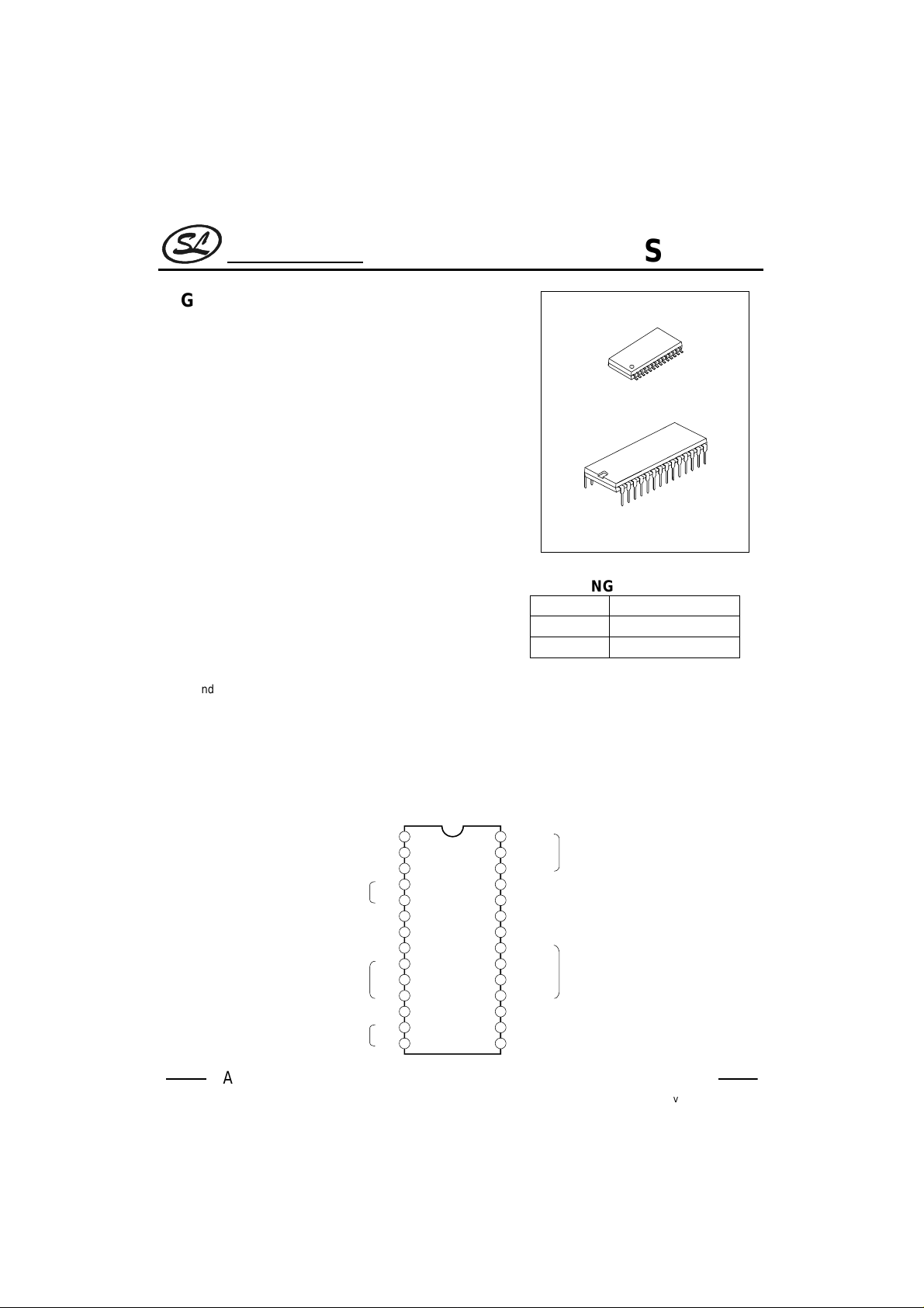
DIP-28
SOP-28
ORDERING INFORMATION
Device Package
SC7313 DIP-28-600-2.54
SC7313S SOP-28-375-1.27
* Loudness function
* Volume control in 1.25dB steps
* Treble and bass control
* Input and output for external equalizer or
noise reduction system
PIN CONFIGURATIONS
SC7313
1
2
3
4
5
6
7
8
9
10
11
12
13
14
28
27
26
25
24
23
22
21
20
19
18
17
16
15
C
REF
GND
V
DD
OUT(R)
R3
R2
R1
LOUD L
L3
L2
SCL
SDA
DIG GND
OUT LF
OUT RF
OUT LR
OUT RR
BOUT(R)
BIN(R)
BOUT(L)
BIN(L)
OUT(L)
IN(L)
L1
L
R
IN(R)
LOUD R
TREBLE
RIGHT
INPUTS
LEFT
INPUTS
) LEFT INPUTS
BUS
INPUTS
BASS
Silan
Semiconductors
SC7313
HANGZHOU SILAN MICROELECTRONICS JOINT-STOCK CO.,LTD
Rev: 1.1 2002.02.26
2
BLOCK DIAGRAM
VOLUME
&LOUDNESS
BASS TREBLE
VOLUME
&LOUDNESS
BASS TREBLE
SERIALBUS DECODER +LATCHES
15
14
13
9
10
11
17 16 12 19 18 4
7 6 8 21 20 5
28
27
26
23
25
24
22
SUPPLY1
2 3
TREBLE
(L)
B-IN
(L)
B-OUT
(L)
LOUDNESS
(L)
IN
(L)
OUT
(L)
LEFT
INPUTS
RIGHT
INPUTS
TREBLE
(R)
B-IN
(R)
B-OUT
(R)
LOUDNESS
(R)
IN
(R)
OUT
(R)
CREF
VDD A-GND
RIGHT
REAR
OUT
RIGHT
FRONT
OUT
DIG-GND
SDA
SCL
LEFT
REAR
OUT
LEFT
FRONT
OUT
BUS
MUTE
SPEAKER
ATT
MUTE
SPEAKER
ATT
MUTE
SPEAKER
ATT
MUTE
SPEAKER
ATT
INPUT SELECTION
& GAIN C ONTROL
ABSOLUTE MAXIMUM RATINGS
Characteristic Symbol Value Unit
Supply Voltage V
S
10.2 V
Operating Temperature Tamb -40~ +85
°C
Storage Temperature Tstg -55 ~ +150
°C
QUICK REFERENCE DATA
Characteristic Symbol Min. Typ. Max. Unit
Supply Voltage Vs 6 9 10 V
Maximum input signal handling V
CL
2Vrms
Total harmonic distortion ,V=1Vrms, f=1kHz THD 0.01 0.1 %
Signal to noise ratio S/N 106 dB
Channel separation, f=1kHz Sc 103 dB
Volume control, 1.25dB step -78.75 0 dB
Bass and treble control, 2dB step -14 +14 dB
Fader and balance control, 1.25dB step -38.75 0 dB
Input gain, 3.75dB step 0 11.25 dB
Mute attenuation 100 dB
Silan
Semiconductors
SC7313
HANGZHOU SILAN MICROELECTRONICS JOINT-STOCK CO.,LTD
Rev: 1.1 2002.02.26
3
ELECTRICAL CHARACTERISTICS
(Refer to the test circuit)
(Tamb=25°C
V
S
=9.0V,R
L
=10kΩ
R
G
=600Ω
all controls flat(G=0), f=1kHz,Unless otherwise specified)
Parameter Symbol Test conditions Min Typ Max Unit
SUPPLY VOLTAGE
Operating Supply Voltage V
S
6 9 10.0 V
Operating Supply Current I
S
20.0 35.0 mA
Ripple rejection of Supply Voltage SVR 60 80 dB
INPUTS SELECTORS
Input resistance R
II
Input 1,2,3 35 50 70
kΩ
Clipping Level V
CL
22.5 Vrms
Input Separation (note 2) S
IN
80 100 dB
Output load resistance R
L
Pin7,17 4
kΩ
Minimum input Gain G
IN(MIN)
-1 0 1 dB
Maximum input gain G
IN(MAX)
11.25 dB
Step resolution G
STEP
3.75 dB
Input noise e
IN
G=11.25dB 2
µV
Adjacent gain steps 4 20 mV
DC steps V
DC
G=18.75 to MUTE 4 mV
VOLUME CONTROL
Input resistance R
IV
20 33 50
kΩ
Control range Crange 70 75 80 dB
Minimum attenuation A
V(min)
-1 0 1 dB
Maximum attenuation A
V(max)
70 75 80 dB
Step resolution A
STEP
0.5 1.25 1.75 dB
A
V
=0 to –20dB -1.25 0 1.25
Attenuation set error E
A
A
V
=-20 to –60dB -3 2
dB
Tracking error E
T
2dB
Adjacent attenuation steps 0 3 mV
DC steps V
DC
From 0dB to A
V
max 0.5 7.5 mV
SPEAKER ATTENUATORS
Control Range Crange 35 37.5 40 dB
Step resolution S
STEP
0.5 1.25 1.75 dB
Attenuation Set error E
A
1.5 dB
Output Mute Attenuation A
MUTE
80 100 dB
Adjacent attenuation steps 0 3 mV
DC steps V
DC
From 0dB to MUTE 1 10 mV
Silan
Semiconductors
SC7313
HANGZHOU SILAN MICROELECTRONICS JOINT-STOCK CO.,LTD
Rev: 1.1 2002.02.26
4
(continued)
Parameter Symbol Test conditions Min Typ Max Unit
BASS CONTROL (note 1)
Control Range G
B
Maximum boost/cut
±12 ±14 ±16
dB
Step resolution B
STEP
123dB
Internal feedback resistance R
B
34 44 58
kΩ
TREBLE CONTROL (note 1)
Control Range Gt Maximum boost/cut
±13 ±14 ±15
dB
Step resolution T
STEP
123dB
AUDIO OUTPUTS
Clipping level V
OCL
THD=0.3% 2 2.5 Vrms
Output load resistance R
L
4
kΩ
Output load capacitance C
L
10 nF
Output resistance R
OUT
30 75 120
Ω
DC voltage level V
OUT
4.2 4.5 4.8 V
GENERAL
BW=20 ~20kHz,flat
output muted
2.5
µV
BW=20 ~20kHz,flat
All gains=0dB
515
µV
Output noise e
NO
A curve, all gains =0 dB 3
µV
Signal to noise ratio S/N All gains=0dB; Vo=1Vrms 106 dB
Av=0,V
IN
=10mV 0.01 0.1 %
Av=-20dB, V
IN
=1Vrms 0.09 0.3 %
Distortion d
Av=-20dB,V
IN
=0.3Vrms 0.04 %
Channel separation left/right Sc 80 103 dB
AV=0 to –20 dB 0 1 dB
Total tracking error
AV=-20 to –60 dB 0 2 dB
BUS INPUTS
Input low voltage V
IL
1V
Input high voltage V
IH
3V
Input current I
IN
-5 +5
µA
Output voltage SDA acknowledge Vo Io=1.6mA 0.4 V
NOTES:
(1) Bass and treble response see Figure 16. The center frequency and quality of the response behavior can be
chosen by the external circuitry. A standard first order bass response can realized by a standard feedback
network.
(2) The selected input is grounded through the 2.2µF capacitor.
 Loading...