

SILAN SC9149A, SC9149AHN, SC9149AL, SC9150A Datasheet
Silan
1
2
Semiconductors
SC9149A/SC9150A
INFRARED REMOTE CONTROL
RECEIVER
DESCRIPTION
The SC9149A/SC9150A are CMOS LSIs designed for use on the
infrared remote control receiver, and when this LSI is used in
combination with SC9148A for transmitter, the remote control
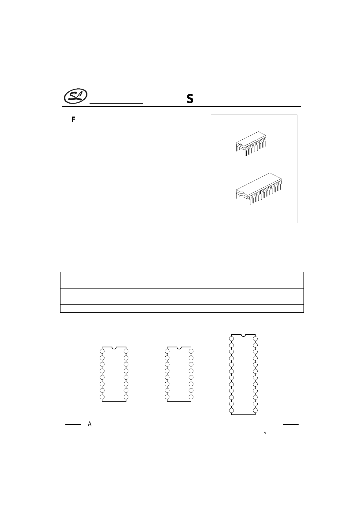
system can be constructed. The SC9149A is DIPcapable of controlling 10 functions, while the SC9150A is DIPtype and is capable of controlling 18 functions.
FEATURES
* Able to output parallel multiple keying signals sent from the
transmitter (The SC9149A is able to output parallel up to 5
functions, while the SC9150A is able to output parallel up to 6
functions.)
* Output for single pulse, hold pulse and cyclic pulse are provided.
(cyclic pulse is available only for SC9150A)
* A single terminal type oscillator by means of CR is provided.
* Code detection circuit provided for code check with the
transmitter prevents inter-ferences from various types of
machines and apparatus.
ORDERING INFORMATION
SC9149A
SC9149AL
SC9149AHN
SC9150A
Advanced version DIP-16 package
Advanced Dependent cyclic (toggle) Outputs
Inversed Rxin input
Output format same as “L”, except that when HP1 or HP2 is active, it will clear CP1.
Advanced version DIP-24 package
PIN CONFIGURATION
GND
1
Rx IN
2
HP1
3
HP2
4
HP3
5
HP4
6
HP5
7
8
SP5 SP4
SC9149A
16
15
14
13
12
11
10
9
VDD
OSC
CODE 2
CODE 3
SP1
SP2
SP3
GND
Rx IN
HP1
HP2
HP3
HP4
HP5
CP2 CP1
6typeandis
1
2
3
4
SC9149AL/
9149AHN
5
6
7
8
16
15
14
13
12
11
10
VDD
OSC
CODE 2
CODE 3
SP1
SP2
SP3
9
DIP-16
SC9149A
4
DIP-24
SC9150A
GND
1
Rx IN
2
HP1
3
HP2
4
HP3
5
HP4
6
SC9150A
HP5
7
8
HP6
9
CP2
10
CP1
11
SP10
12 13
SP9 SP8
VDD
24
OSC
23
CODE 1
22
CODE 2
21
SP1
20
SP2
19
SP3
18
17
SP4
16
SP5
15
SP6
14
SP7
HANGZHOU SILAN MICROELECTRONICS JOINT-STOCK CO.,LTD
Rev: 1.0 2000.12.31
1
Silan
Semiconductors
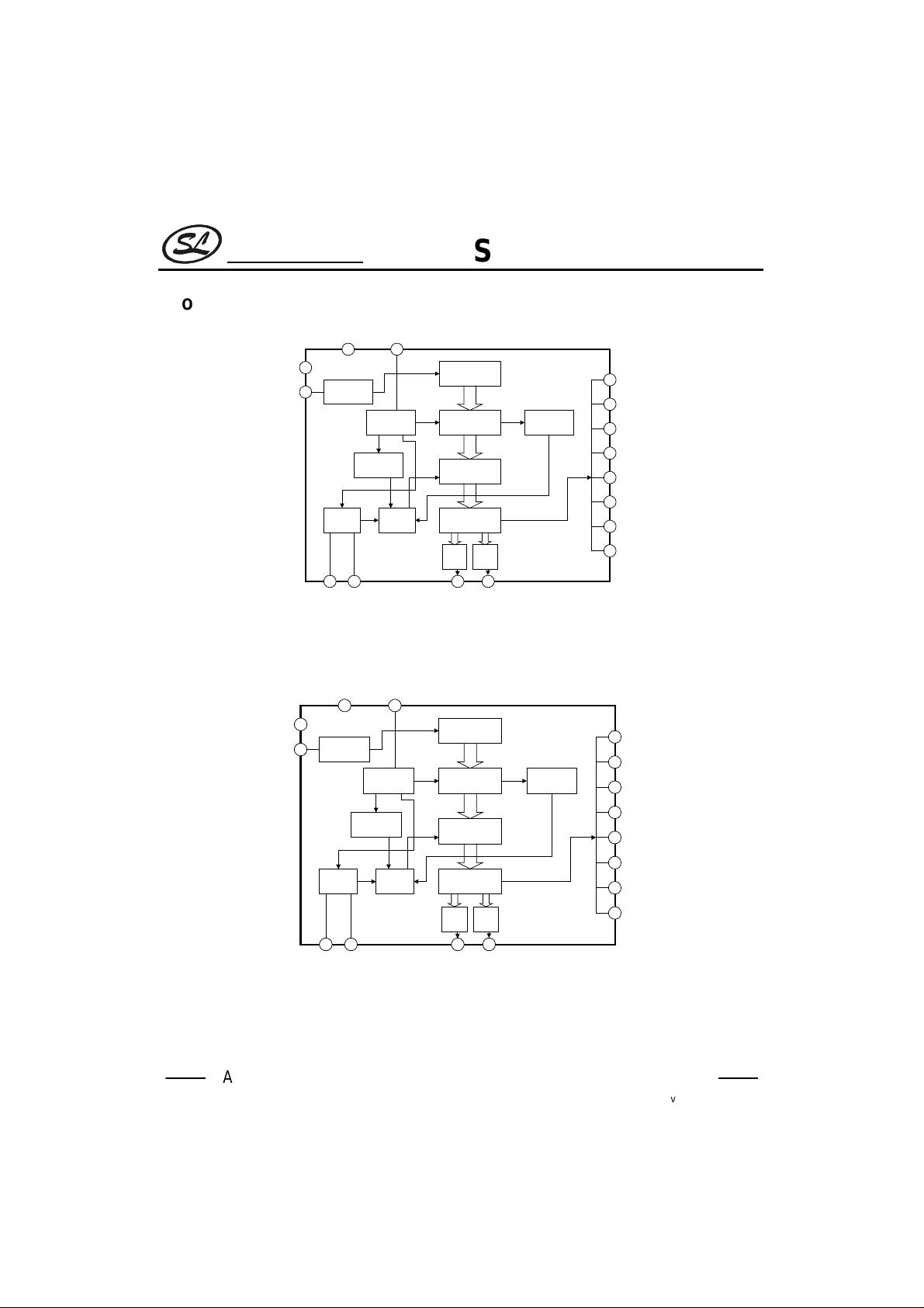
BLOCK DIAGRAM
SC9149A/SC9150A
GND Rx IN
16
VDD
OSC
OSC
15
Code
Check
CODE 2 CODE 3 SP1 SP2
Input shift
register
Input Pulse
counter
Detection
Error
21
Up Counter
Shift register Data Check
Latch Circuit
Output Buffer
F/F F/F
11121314
HP1
3
HP2
4
HP3
5
HP4
6
HP5
7
8
SP5
9
SP4
10
SP3
SC9149A Block Diagram
GND Rx IN
16
VDD
OSC
15
OSC
Code
Check
CODE 2 CODE 3 SP1 SP2
Input shift
register
Input Pulse
counter
Detection
Error
21
Up Counter
Shift register Data Check
Latch Circuit
Output Buffer
F/F F/F
11121314
HP1
3
4
HP2
5
HP3
6
HP4
7
HP5
8
CP2
9
CP1
10
SP3
SC9149AL/9149AHN Block Diagram
HANGZHOU SILAN MICROELECTRONICS JOINT-STOCK CO.,LTD
Rev: 1.0 2000.12.31
2
Silan
Semiconductors
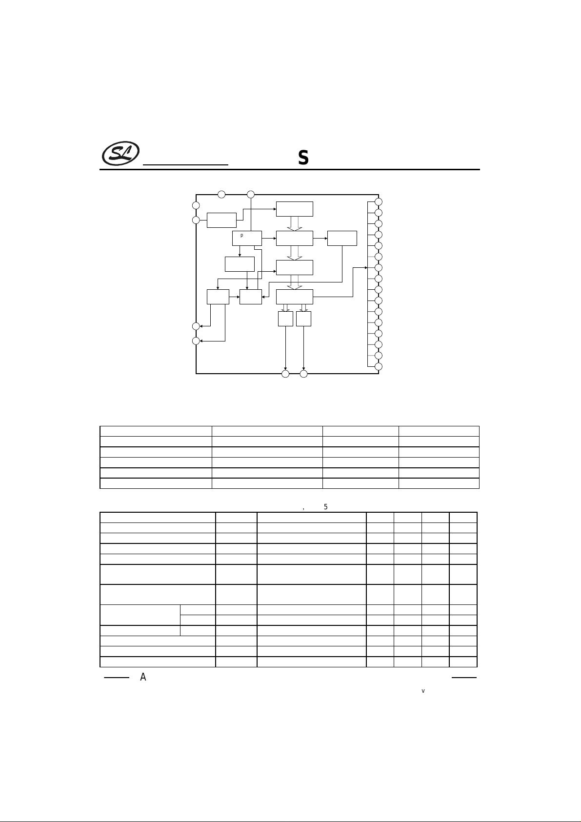
VDD
OSC
CODE 1
CODE 2
24
23
22
21
GND Rx IN
OSC
Code
Check
21
Input shift
register
Input Pulse
counter
Error
Detection
SC9150A Block Diagram
ABSOLUTE MAXIMUM RATINGS
Characteristic Symbol Value Unit
Supply Voltage V
Input / Output Voltage VIN,V
PowerDissipation P
Operating Temperature Tamb -20 ~ +75
Storage Temperature Tstg -55 ~ +125
(Ta=25°C)
DD
D
ELECTRICAL CHARACTERISTICS
Parameter Symbol Test Conditions Min Typ Max Unit
Operating Supply Voltage V
Operating Supply Current I
Standard OSC Frequency Sfosc 38 kHz
Oscillation Frequency fosc 27 57 kHz
Variance Of Oscillation Frequency
By VDD
Variance Of Oscillation Frequency
By Temperature
Output Current
“H” Level I
“L” Level I
Input Current “H” Level I
Pull-Up Resistor Rup CODE Terminal 10 20 40
Input Circuit Threshold Voltage V
Hysteresis Width V
∆V
∆T
(Tamb=25°CVDD=5.0V,Unless otherwise specified)
Ta=25 ~ 75°C
DD
Output without Load 1.0 mA
DD
fosc V
DD
Ta=-30~+75°C
fosc
All output, VOH=4.0V -1.0 mA
OH
All Output, VOL=1V 1.0 mA
OL
CODE Terminal, VIH=5.0V -1.0 1.0
IH
Rx Terminal 2.0 2.5 3.0 V
IN
Rx Terminal 0.8 V
HIS
HANGZHOU SILAN MICROELECTRONICS JOINT-STOCK CO.,LTD
SC9149A/SC9150A
HP1
Up Counter
Shift register Data Check
Latch Circuit
Output Buffer
F/F F/F
20 19
SP1 SP2
OUT
Vss-0.3V ~ VDD+0.3V V
=4.5~5.5V -5 5 %
3
3
HP2
4
HP3
5
6
HP4
7
HP5
8
HP6
9
CP2
10
CP1
SP10
11
SP9
12
SP8
13
14
SP7
15
SP6
16
SP5
17
SP4
18
SP3
0~6.0 V
200 mW
°C
°C
4.5 5.5 V
-5 5 %
Rev: 1.0 2000.12.31
µA
kΩ
Silan
Semiconductors
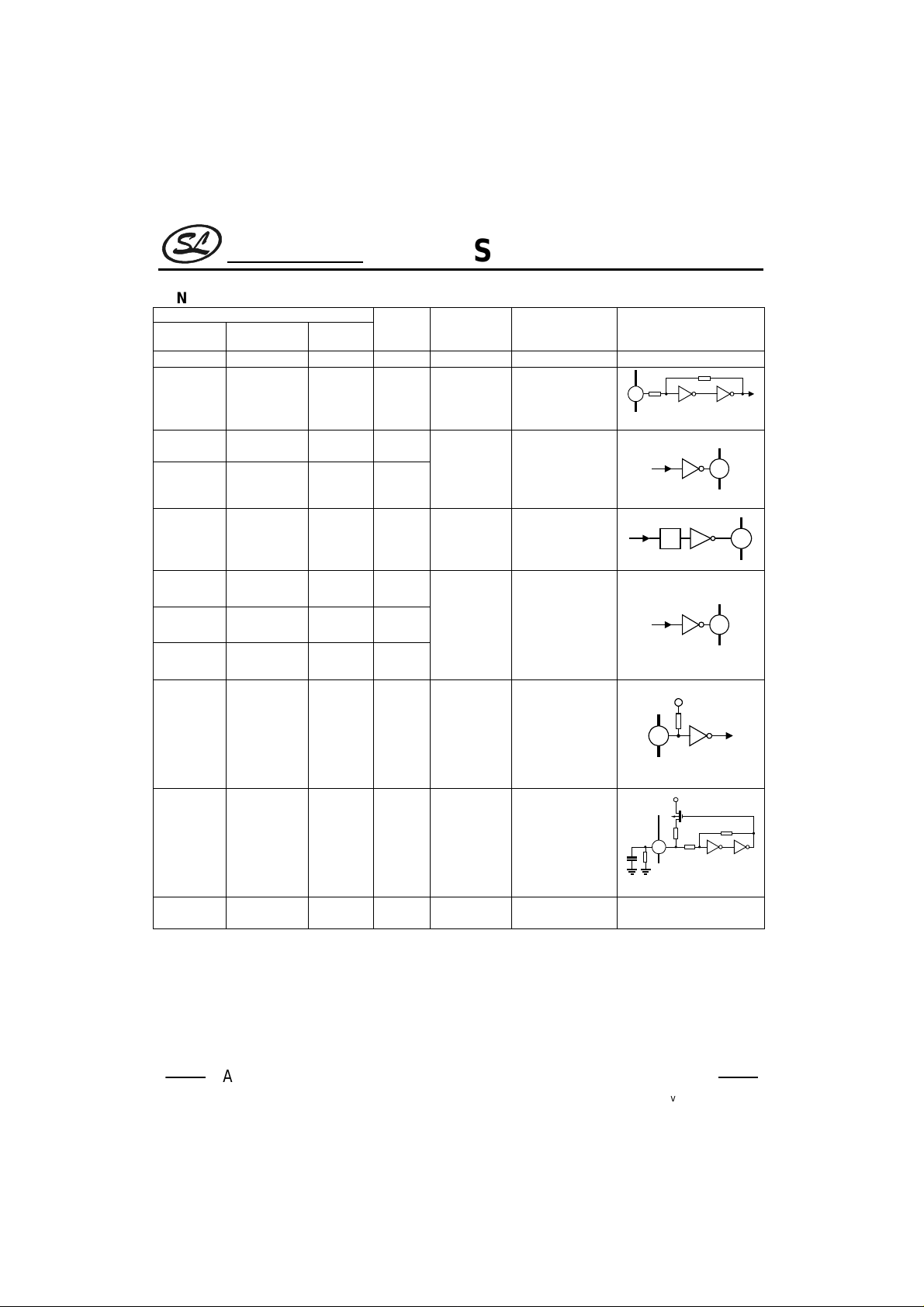
PIN DESCRIPTION
Pin No.
SC9149A
111GNDGND
222RxIN
3~7 3~7 --
-- -- 3~8
-- 9~8 9~10
-- 12~10 --
8~12 -- --
-- -- 11~20
13,14 13~14 21~22 CODE Code input
15 15 23 OSC
16 16 24 V
SC9149AL
/9149AHN
SC9150A
Symbol Terminal
Receiving
signal input
HP1
~HP5
HP1
~HP6
CP1
~CP2
SP1
~SP3
SP1
~SP5
SP1
~SP10
DD
Continuous
signal
output
Cyclic
signal
output
Single-shot
signal
output
Timing
oscillation
Power
supply
SC9149A/SC9150A
Function
/operation
Instruction signal
with carrier
signal eliminated
is input.
As long as
receiving signal
is input, this
output is held at
“H” level
When receiving
signal is input,
output is
reversed.
When receiving
signal is input,
output is placed
at “H” level only
for a fixed
time.(about
107msec)
Transmitter code
is compared with
a code set at
this terminal and
if they agree
each other, input
is accepted.
A resistor and a
capacitor are
parallel
connected
between this
terminal and
GND.
Input/output
configuration
F/F
V
DD
Built-in pull-up resistor.
V
DD
HANGZHOU SILAN MICROELECTRONICS JOINT-STOCK CO.,LTD
Rev: 1.0 2000.12.31
4
 Loading...