

Silan
Semiconductors
EXTENDED VOLTAGE CALLING
NUMBER IDENTIFICATION CIRCUIT 2
DESCRIPTION
The SC88E43 Calling Number Identification Circuit 2(ECNIC2) is
a low power CMOS integrated circuit intended for receiving physical
layer signals transmitted according to BT (British Telecom) SIN227
& SIN242, the U.K.’s CCA (Cable Communications Association)
TW/P&E/312 and Bellcore GR-30-CORE & SR-TSV-002476
specifications. The SC88E43 is suitable for applications using a
fixed voltage power source between 3 and 5V ±10%.
SC88E43
DIP-24
FEATURES
* Compatible with:
-- British Telecom (BT) SIN227 & SIN242
-- U.K.’s Cable Communications Association (CCA)
specification TW/P&E/312
-- Bellcore GR-30-CORE (formerly known as TR-NWT-000030)
& SR-TSV-002476
* Bellcore “CPE” Alerting Signal” (CAS) and BT “Idle State
Tone Alert Signal” detection
* Ring and line reversal detection
* 1200 baud Bell 202 and CCITT V.23 Frequency Shift Keying
(FSK) demodulation
* 3 or 5V ±10% supply voltage
* High input sensitivity (-40dBv Tone and FSK Detection)
* Selectable 3-wire FSK data interface
(microcontroller or SC88E43 controlled)
* Low power CMOS with powerdown mode
* Input gain adjustable amplifier
* Carrier detect status output
* Uses 3.58 MHz crystal
RECOMMENDED OPERATING CONDITIONS
Parameter Symbol Min Typ Max Unit
Power Supplies V
Clock Frequency f
Tolerance on Clock Frequency
Operating Temperature T
DD
OSC
∆f
C -0.1 -- +0.1 %
OP
SOP-24
APPLICATIONS
* BT Calling Line Identity Presentation
(CLIP), CCA CLIP, and Bellcore Calling
Identity Delivery (CID) systems
* Feature phones, including Analog
Display Services Interface (ADSI)
phones
* Phone set adjunct boxes
* FAX and answering machines
* Database query and Computer
Telephony Integration (CTI) systems
ORDERING INFORMATION
SC88E43
SC88E43S
(Ta=25°C ; Voltages are with respect to VSS)
2.7 -- 5.5 V
-- 3.579545 -- MHz
-40 -- 85
24 Pin DIP
24 Pin SOIC
°C
HANGZHOU SILAN MICROELECTRONICS JOINT-STOCK CO.,LTD
Rev: 1.0 2000.12.31
1
Silan
Semiconductors
PIN CONFIGURATION
BLOCK DIAGRAM
TRIGin
TRIGRC
TRIGout
MODE
OSCO
IN+
IN-
GS
VRef
CAP
OSCI
Vss
1
2
3
4
5
6
7
8
9
10
11
12
SC88E43
SC88E43
VDD
24
23
St/GT
22
ESt
21
StD
20
INT
19
CD
18
DR
17
DATA
DCLK
16
FSKen
15
PWDN
14
IC
13
MODEFSKen
1
IN+
IN-
GS
VRef
CAP
PWDN
+
2
-
3
4
Generator
5
14
OSCin OSCout TRIGin
Anti-alias
Filter
To internal cct.
Bias
Alert Signal High
To internal cct.
Oscillator
10 11 6 7 8
Alert Signal Low
FSK Bandpass
Filter
Tone Filter
Tone Filter
TRIGRC
Demodulator
TRIGout
FSK
Carrier
Detector
Tone
Detection
Algorithm
Data
Timing
Recovery
Interrupt
Generator
Guard
Time
HANGZHOU SILAN MICROELECTRONICS JOINT-STOCK CO.,LTD
2
915
16
17
18
19
20
21
23
22
24
12
Rev: 1.0 2000.12.31
DCLK
DATA
DR
CD
INT
StD
St/GT
ESt
VDD
VSS
Silan
Semiconductors
ABSOLUTE MAXIMUM RATINGS
Characteristic Symbol Value Unit
Supply Voltage V
Voltage on any pin other than supplies* V
Current at any pin other than supplies I
Storage Temperature Tstg -65 ~ +150
* Under normal operating conditions voltage on any pin except supplies can be minimum VSS -1V to
maximum V
DD +1V for an input current limited to less than 200mA.
(Voltages are with respect to VSS, unless otherwise stated).
DD
PIN
PIN
-0.3 ~ 6.0 V
Vss-0.3V ~ VDD+0.3V V
DC ELECTRICAL CHARACTERISTICS
Parameter Symbol Test conditions Min Typ Max Unit
All input are VDD/V
except for oscillator pins.
Stand-by Supply Current I
DDQ
No analog input.
Outputs unloaded.
PWDN = V
All input are VDD/V
Operating
Supply Current
VDD=5V±10%
V
=3V±10%
DD
except for oscillator pins.
No analog input.
I
DD
Outputs unloaded.
PWDN = V
FSKen = V
Power Consumption P
Schmitt Input High Threshold V
Schmitt Input Low Threshold V
Schmitt Hysteresis V
O
T+
T-
HYS
TRIGin,
TRIGin,
TRIGin,
TRIGRC
TRIGRC
TRIGRC
CMOS Input High Voltage VIHDCLK,MODE,FSKen Pins 0.7V
CMOS Input Low Voltage VILDCLK,MODE,FSKen Pins V
VOH=0.9V
Output High Sourcing Current I
OH
TRIGout
CD
,DCLK,DADA,
,StD,Est,St/GT Pins
VOL=0.1V
Output Low Sinking Current I
OL
TRIGout
CD
,DCLK,DATA,
, StD, Est,St/GT,
TRIGRC
VIN=VDDto V
I
IN1
Input Current
IN+,IN-,TRIGin Pins
VIN=VDDto V
I
IN2
PWDN,DCLK,MODE,FSKen
SS
-- 0.5 15
DD.
SS
-- 4.7 8 mA
SS;
DD.
-- 2.5 4.5 mA
-- -- -- 44 mW
DD
DD
INT
SS
SS
,PWDN Pins
,PWDN Pins
,PWDN Pins
Pins
DR
DR
0.48V
0.28V
0.2 -- -- V
,
0.8 -- -- mA
,
2----mA
-- -- 1
-- -- 10
SC88E43
10 mA
-- 0.68V
SS
DD
DD
DD
-- 0.48V
-- V
-- 0.3V
DD
DD
DD
DD
(To be continued)
°C
µA
V
V
V
V
µA
µA
HANGZHOU SILAN MICROELECTRONICS JOINT-STOCK CO.,LTD
Rev: 1.0 2000.12.31
3
Silan
Semiconductors
(continued)
Parameter Symbol Test conditions Min Typ Max Unit
V
Output High-Impedance Current
Output Voltage V
Output Resistance R
Comparator Threshold Voltage V
=VDDto V
I
I
I
OUT
OZ1
TRIGRC
V
=VDDto V
OUT
OZ2
OZ3
REF
REF
TGt
Pin.
INT
V
=VDDto V
OUT
St/GT Pin.
No load.
Vref Pin
Vref Pin -- 2
St/GT Pin
Pin.
SS,
SS,
SS,
-- -- 1
-- -- 10
-- -- 5
0.5V
-0.05
0.5V
0.05
AC ELECTRICAL CHARACTERISTICS
Parameter Symbol Conditions Min Typ Max Unit Notes
Dual Tone Alert Signal Detection
Low Tone Frequency f
High Tone Frequency f
L
H
-- 2130 -- Hz
-- 2750 -- Hz
Frequency Deviation accept 1.1% -- -- -- 4
Frequency Deviation Reject 3.5% -- -- -- 5
Accept Signal Level Per Tone
Rejet Signal Level Per Tone
Positive And Negtive Twist
Accept
Signal to Noise Ratio SNR
TONE
Timming Parameter Measurement Voltage Levels
CMOS Threshold Voltage V
Rise/Fall Threshold Voltage High
Rise/Fall Threshold Voltage Low V
CT
V
HM
LM
-40 -- -2
-37.78 -- 0.22
-- -- -46 dBV
-- -- -43.78 dBm
7----
20 -- -- dB 1,2
-- 0.5V
-- 0.7V
-- 0.3V
Gain Setting Amplifier
Input Leakage Current I
IN
VSS≤ VIN≤ V
DD -- -- 1
Input Resistance RIN-- 10 -- -Input Offset Voltage V
Power Supply Rejection Ratio PSRR 1kHz ripple on V
-- -- -- 25 mV
OS
DD
40 -- -- dB
SC88E43
0.5V
--
0.5V
--
-- V
-- V
-- V
(To be continued)
DD
DD
-
DD
DD
DD
+0.05
+0.05
dBV
dBm
dB
µA
MΩ
DD
DD
a
b
c
µA
µA
µA
V
kΩ
V
3
3
HANGZHOU SILAN MICROELECTRONICS JOINT-STOCK CO.,LTD
Rev: 1.0 2000.12.31
4
Silan
Semiconductors
(continued)
Parameter Symbol Conditions Min Typ Max Unit Notes
V
Common Mode Rejection CMRR
DC Open Loop Voltage Gain A
Unity Gain Bandwidth fC-- 0.3 -- -- MHz
Output Voltage Swing V
Maximum Capacitive Load (GS) CL-- -- -- 100 pF
Maximum Resistive Load (GS) RL-- 50 -- -Common Mode Range Voltage V
VOL
O
CM
≤ VIN≤ V
CMmin
-- 30 -- -- dB
Load ≥ 50kΩ
-- 1.0 -- VDD-0.1 V
CMmax 40 -- -- dB
0.5 -- V
FSK Detection
-- -40 -- -8
Input Detection Level
Transmission Rate -- 1188 1200 1212 baud
Input Frequency Detection
Signal to Noise Ratio SNR
-- -37.78 -- -5.78
-- 10 -- 398.1 mVrms
Bell 202 1 (Mark) 1188 1200 1212 Hz
Bell 202 0 (Space) 2178 2200 2222 Hz
CCITT V.23 1 (Mark) 1280.5 1300 1319.5 Hz
CCITT V.23 0 (Space) 2068.5 2100 2131.5 Hz
-- 20 -- -- dB 6,7
FSK
Dual Tone Alert Signal Timing
Alert Signal Present Detect Time t
Alert Signal Absent Detect Time t
-- 0.5 -- 10 ms 9
DP
-- 0.1 -- 8 ms 9
DA
3-Wire Interface Timming
Power-up Time t
Power-downTime t
Input FSK to
Input FSK to
Hysteresis
CD
CD
Low Delay
High Delay
PU
PWDN, OSC1 Pins
PD
t
CP
CD
t
CA
Pin
-- -- 50 ms
-- -- 1 ms
-- -- 25
8---8----ms
3-Wire Interface Timming (Mode 0)
RiseTime t
Fall Time t
Low Time
Rate -- DATA Pin 1188 1200 1212 baud 11
Input FSK to DATA delay t
RR DR
RF DR
tRL
IDD
Pin
Pin
Pin
DR
DATA Pin -- 1 5 ms
-- -- 200
-- -- 200
415 416 417
SC88E43
-0.5 V
DD
PP
kΩ
a
dBV
b
ms
ms
ns 10
ns 10
µs
6,8
12
dBm
(To be continued)
HANGZHOU SILAN MICROELECTRONICS JOINT-STOCK CO.,LTD
Rev: 1.0 2000.12.31
5
Silan
Semiconductors
(continued)
Parameter Symbol Conditions Min Typ Max Unit Notes
Rise time t
Fall Time t
DATA to DCLK delay t
DCLK to DATA delay t
Frequency f
High Time t
Low Time t
DCLK to
DR
delay
R
F
DCD
CDD
DCLK0
CH
CL
t
CRD
DATA, DCLK Pins
DCLK Pin
DCLK ,
DR
Pin
3-Wire Interface Timming (Mode 1)
Frequency f
Duty Cycle 30 -- 70 %
RiseTime t
Rate t
Input FSK to DATA delay t
a. dBV= decibels above or below a reference voltage of 1Vrms. Signal level is per tone.
b. dBm = decibels above or below a reference power of 1mW into 600 ohms. 0dBm = 0.7746Vrms. Signal
level is per tone.
c. Twist = 20 log (f
H amplitude / fL amplitude).
DCLK1
R1
DDS
DDH
DCLK Pin
DCLK ,
DR
Pin
-- -- 200 ns 10
-- -- 200 ns 10
6 416 --
6 416 --
1201.6 1202.8 1204 Hz 12
415 416 417
415 416 417
415 416 417
-- -- 1 MHz
-- -- 20 ns
500 -- -- ns
500 -- -- ns
SC88E43
µs
µs
µs
µs
µs
11,12,
13
11,12,
13
12
12
12
Notes:
1. Both tones have the same amplitude.
2. Band limited random noise 300-3400Hz. Measurement valid only when tone is present.
3. With gain setting as shown in Figure 10. Production tested at V
DD =3V±10%, 5V±10%.
4. Range within which tones are accepted.
5. Ranges outside of which tones are rejected.
6. Both mark and space have the same amplitude.
7. Band limited random noise (200-3400Hz). Present when FSK signal is present. Note that the BT band is
300-3400Hz, the Bellcore band is 0-4kHz.
8. Production tested at V
DD =5V±10%, 3V±10%.
9. Refer to Figure 16 and 19.
10. into 50pF load.
11. FSK input data at 1200±12 baud.
12. OSCI at 3.579545 MHz±0.1%.
13. Function of signal condition.
HANGZHOU SILAN MICROELECTRONICS JOINT-STOCK CO.,LTD
Rev: 1.0 2000.12.31
6
Silan
Semiconductors
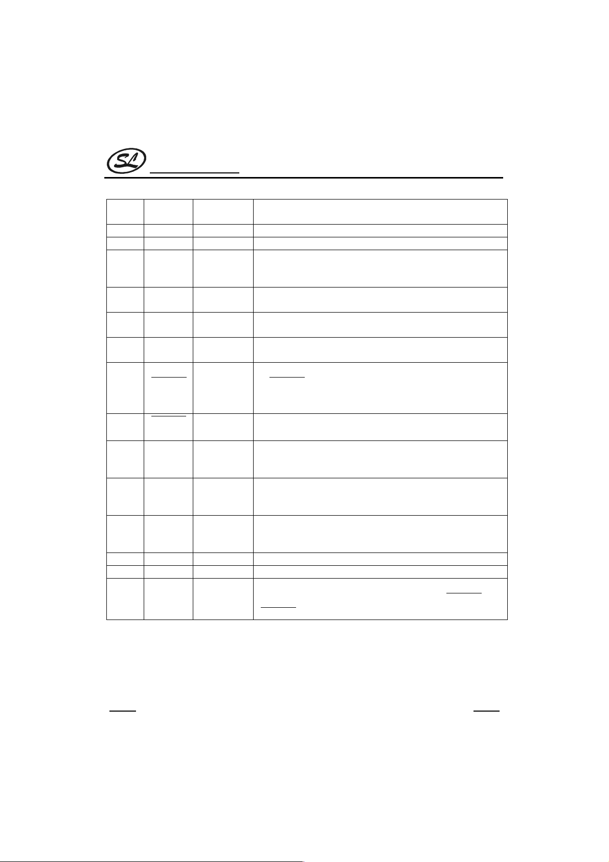
PIN DESCRIPTION
Pin
No.
10 OSCI Input
11 OSCO Output
12 Vss -- Power Supply Ground.
13 IC -- Internal Connection. Must be connected to VSS for normal operation.
14 PWDN Schmitt Input
Symbol I/O Function
1 IN+ Input Non-inverting Input of the internal opamp.
2 IN- Input Inverting Input of the internal opamp.
Gain Select of internal opamp. The opamp’s gain should be set
3 GS Output
4VRef Output
5CAP --
6 TRIGin Trigger Input
TRIGRC
7
TRIGout
8
9 MODE CMOS Input
Open Drain
Output /
Schmitt Input
CMOS Output
according to the nominal Vdd of the application using the information
in Figure 10.
Reference Voltage. Nominally VDD/2. It is used to bias the input
opamp.
Capacitor. A 0.1mF decoupling capacitor should be connected across
this pin and V
Trigger Input. Schmitt trigger buffer input. Used for line reversal and
ring detection.
Trigger RC. Used to set the (RC) time interval from TRIGin going low
TRIGout going high. An external resistor connected to VDD and
to
capacitor connected to V
interval.
Trigger Out. Schmitt trigger buffer output. Used to indicate detection of
line reversal and/or ringing.
3-wire interface: Mode Select. When low, selects FSK data interface
mode 0. When high, selects FSK data interface mode 1. See pin 16
(DCLK) description to understand how MODE affects the DCLK pin.
Oscillator Input. A 3.579545MHz crystal should be connected between
this pin and OSCO. It may also be driven directly from an external
clock source.
Oscillator Output. A 3.579545MHz crystal should be connected
between this pin and OSCI. When OSCI is driven by an external clock,
this pin should be left open.
Power Down. Active high. When high, the device consumes minimal
power by disabling all functionality except TRIGin,
SS.
SS determine the duration of the (RC) time
TRIGout Must be pulled low for device operation.
HANGZHOU SILAN MICROELECTRONICS JOINT-STOCK CO.,LTD
7
SC88E43
TRIGRC and.
(To be continued)
Rev: 1.0 2000.12.31
Silan
Semiconductors
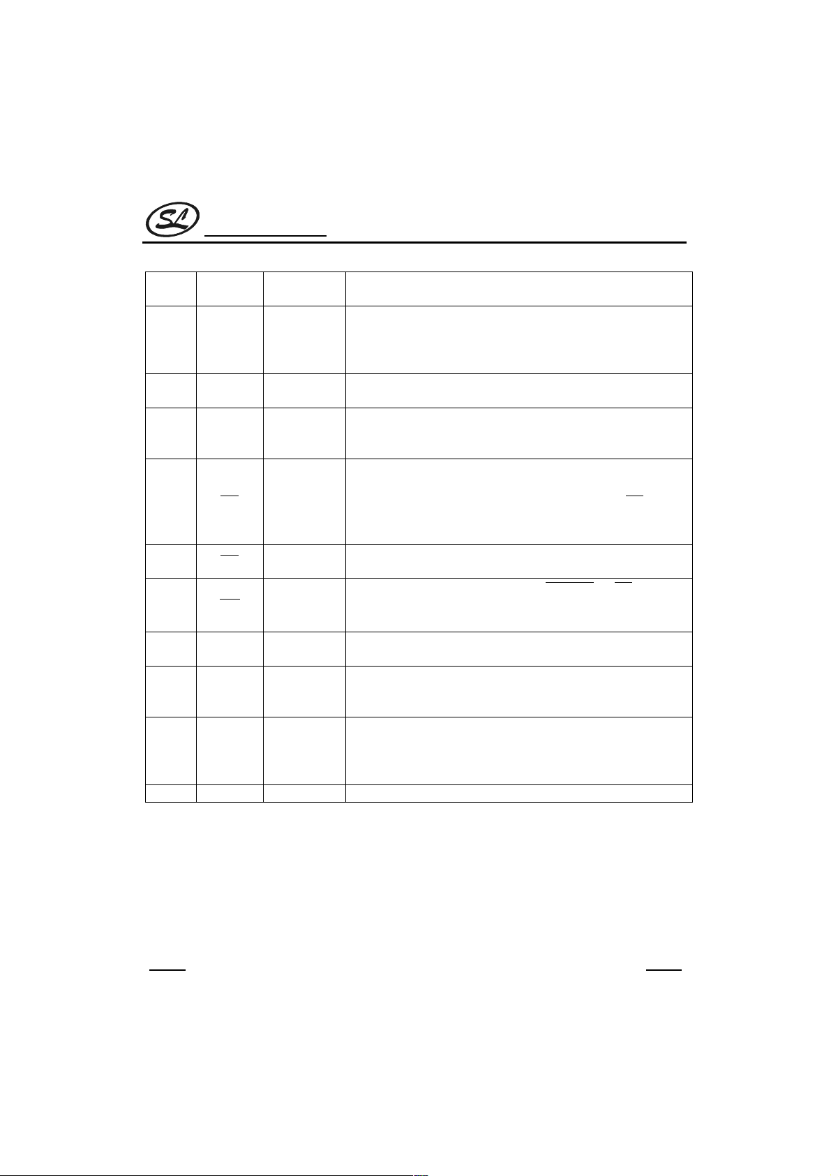
(continued)
Pin
No.
15 FSKen CMOS Input
16 DCLK
17 DATA CMOS Output
18
19
20
21 StD CMOS Output
22 ESt CMOS Output
23 St/GT
24 VDD -- Positive Power Supply.
Symbol I/O Function
Input/Output
DR
CD
INT
CMOS Output
CMOS Output
Open Drain
Analog Input /
CMOS Output
CMOS
Output
FSK Enable. Must be high for FSK demodulation. This pin should be
set low to prevent the FSK demodulator from reacting to extraneous
signals (such as speech, alert signal and DTMF which are all in the
same frequency band as FSK).
3-wire Interface: Data Clock. In mode 0 (MODE pin low), this pin is an
output. In mode 1 (MODE pin high), this pin is an input.
3-wire Interface: Data. In mode 0 the FSK data appears at the pin
once demodulated. In mode 1 the FSK data is shifted out on the rising
edge of the microcontroller supplied DCLK.
3-wire Interface: Data Ready. Active low. In mode 0 this output goes
low after the last DCLK pulse of each data word. This identifies the 8bit word boundary on the serial output stream. Typically,
to latch 8-bit words from a serial-to-parallel converter into a
microcontroller. In mode 1 this pin will signal the availability of data.
Carrier Detect. Active low. A logic low indicates the presence of inband signal at the output of the FSK bandpass filter.
Interrupt. Active low. It is active when
StD is high. This output stays low until all three signals have become
inactive.
Dual Tone Alert Signal Delayed Steering Output. When high, it
indicates that a guard time qualified alert signal has been detected.
Dual Tone Alert Signal Early Steering Output. Alert signal detection
output. Used in conjunction with St/GT and external circuitry to
implement the detect and non-detect guard times.
Dual Tone Alert Signal Steering Input/Guard Time. A voltage greater
than V
TGt (see figure 4) at the St/GT pin causes the device to indicate
that a dual tone has been detected by asserting StD high. A voltage
less than V
TGt frees the device to accept a new dual tone.
SC88E43
DR is used
TRIGout or DR is low, or
HANGZHOU SILAN MICROELECTRONICS JOINT-STOCK CO.,LTD
Rev: 1.0 2000.12.31
8
 Loading...