

SILAN SC84510BP, SC84510CP, SC84510DP, SC84510EP, SC84510FP Datasheet
...
Silan
Semiconductors
PS/2 SCROLLING MOUSE
CONTROLIER
DESCRIPTION
The SC84510 Scrolling Mouse Controller is specially designed to
control PS/2 mouse device. This single chip can interface three keyswitches four photo-couples plus x-axis direct to 8042 controller.
SC84510 can receive command and echo status or data format
which are compatible with IBM PS/2 mode mouse.
Key debouncing circuit is provided to prevent false entry and
improve the accuracy.
In the traditional mouse, a great number of noises are generated
when the grid is partially closed or opened. These noises are usually
mistaken for movement signals by traditional mouse controller and
the cursor of the display screen is thus moved frequently up and
down or back and forth. This will consume a great amount of energy.
The SC84510 mouse controller provides noise immunity circuits to
eliminate these noises in order to reduce energy consumption.
SC84510
DIP-16
FEATURES
* Using 50k ±5% resistor for RC oscillation.
* Compatible with legacy PS/2 mouse.
* Compatible with Microsoft scrolling mouse.
* Built-in noise immunity circuit.
* Built-in current comparator for photo-couples input.
* Built-in three steps dynamic input impedance.
* Three key-switches and four photo-couples inputs.
* Both key-press and key-release debounce interval 12 ms.
* The sampling rate of motion detector is about 65KHz.
ORDERING INFORMATION
SC84510AP DIP-16 Package, Photo couples input. (Z/1)
SC84510BP DIP-16 Package, Key-switches input.
SC84510CP DIP-16 Package, Voltage-sensing input.
SC84510DP DIP-16 Package, Mechanical input. (Z/1)
SC84510EP DIP-16 Package, Photo couples input. (Z/4)
SC84510FP DIP-16 Package, Mechanical input. (Z/2)
HANGZHOU SILAN MICROELECTRONICS JOINT-STOCK CO.,LTD
* Low power dissipation.
* Six types Z direction input:
1. Photo couples input. (Z/1)
2. Key-switches input.
3. Voltage-sensing input.
4. Mechanical input. (Z/1)
5. Photo couples input. (Z/4)
6. Mechanical input. (Z/2)
Rev: 1.0 2000.12.31
1
Silan
Semiconductors
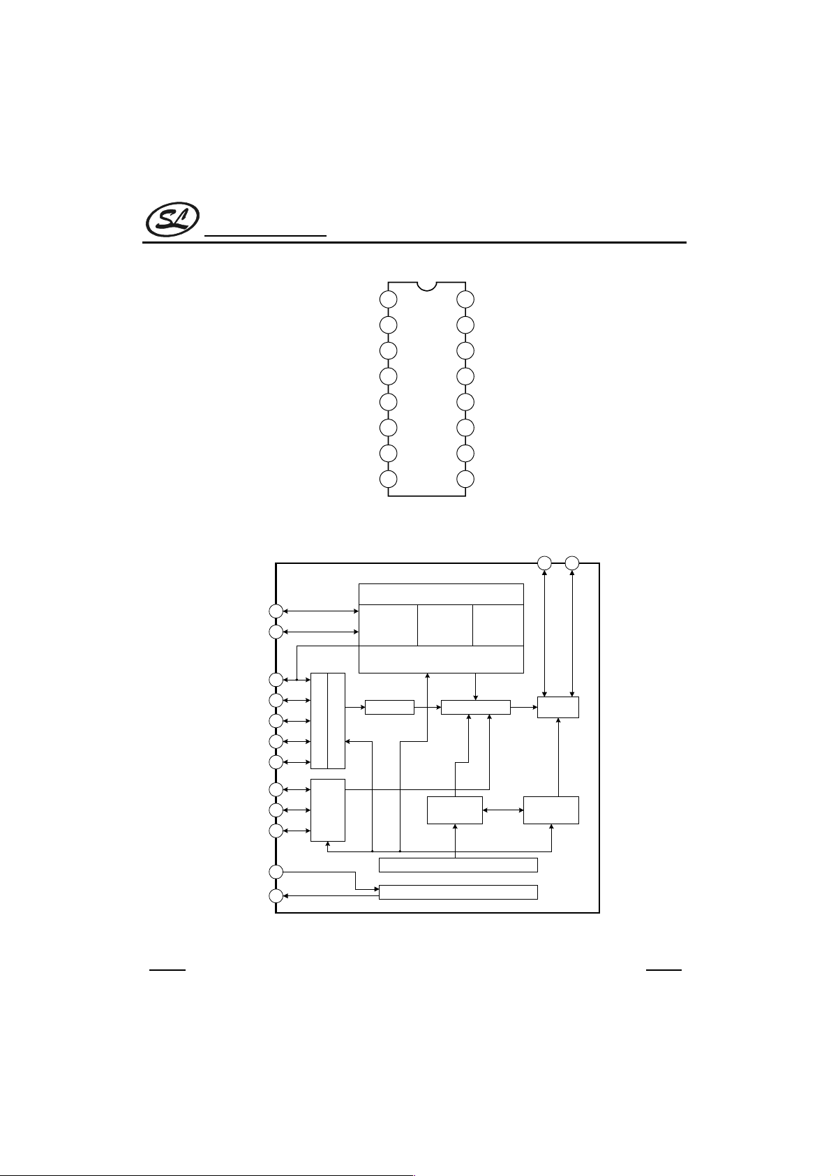
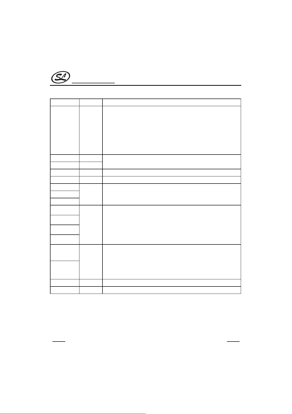
PIN CONFIGURATIONS
SC84510
BLOCK DIAGRAM
Z1
Z2
OPT
X1
X2
Y1
Y2
VDD
OSC OUT
Z1
Z2
CLK
DATA
1
2
3
4
5
6
16
15
14
13
12
11
OSCR
Y2
Y1
X2
X1
L
SC84510A/ B/C/E /F
OPT
VSS
7
8
10
M
R
9
DATA CLK
6 5
THREE TYPESSELECTOR
3
4
7
12
13
14
15
COMPARATOR
COMPARATOR
DETECTOR
COUNTER MULTIPLEXER
VOLTAGE
SENSOR
Z-AXIS COUNTER
KEY-SWITCH
DETECTOR
DATA
I/O
L
OSCR
OSC.OUT
11
M
10
R
9
16
2
DEBOUNCE
COMMAND
STATUS
SYSTEM CLOCK GENERATOR
RC &CRYSTAL OSCILLATION
TIMING
CONTROLLER
HANGZHOU SILAN MICROELECTRONICS JOINT-STOCK CO.,LTD
Rev: 1.0 2000.12.31
2
Silan
Semiconductors
ABSOLUTE MAXIMUM RATINGS
Characteristic Symbol Value Unit
Temperature Under Bias T
Storage Temperature range T
Input Voltage V
Output Voltage V
(Tamb=25°C, unless otherwise specified)
OPR
STR
IN
O
0~70
-65 ~ +150
-0.3 ~ +6.0 V
-0.3 ~ +6.0 V
DC ELECTRICAL CHARACTERISTICS
Parameter Symbol Min Typ Max Unit
Operating Voltage V
Operating Current (No Load) Iop -- -- 1.2 mA
CLK, DATA
Positive-going Threshold Voltage
CLK, DATA
Negative-going Threshold Voltage
DATA, CLK Input Current (pull up resistor) (Vin=0V) Idc 0.56 -- 1.86 mA
DATA, CLK Low Output Voltage (Iprl=-4mA) Vprl -- -- 0.4 V
X1, X2, Y1, Y2, Z1, Z2 (Photo Mode)
Low Input Reference Current
X1, X2, Y1, Y2, Z1, Z2 (Photo Mode)
High Input Reference Current
X1, X2, Y1, Y2, Z1, Z2 (Photo Mode)
Input Current (Input Impedance) (80µA)
X1, X2, Y1, Y2, Z1, Z2 (Photo Mode)
Input Current (Input Impedance) (500µA)
L, M, R, OPT, Z1, Z2 (Key Mode) Input Low Voltage Vail -- -- 0.3 V
L, M, R, OPT, Z1, Z2 (Key Mode) Input High Voltage Vaih 0.7 V
L, M, R, Z1, Z2 (Key & Voltage Mode)
Input Resistor (Vin=V
OPT Input Resistor (Vin=VDD) Rxi 133 -- 400 kΩ
OPT High Output Current (Vin=VDD) Vopt 4.5 -- -- V
L, M, R, X1, X2, Y2, Y2, Z1, Z2
Input Leakage Current (Vin=0V)
OPT High Output Current (Iopt=10mA)
(Tamb=25~70°C)
DD
Vt+ 0.6V
Vt- 0.2 V
Ipl 60 -- -- µA
Iph -- -- 110 µA
Vpi 0.8 -- 1.2 V
Vpi 1.5 -- 2.8 V
Rmi 92 -- 310 kΩ
)
DD
Iil 0 -- -1.0 µA
VDD=4.5V 3.2 -- --
VDD=5V 4.5 -- -- V
V
=5.5V
DD
Idc
4.5 5 5.5 V
DD
5.5 -- --
SC84510
-- 0.8 V
-- 0.4 V
DD
-- -- V
DD
DD
DD
DD
°C
°C
V
V
V
HANGZHOU SILAN MICROELECTRONICS JOINT-STOCK CO.,LTD
Rev: 1.0 2000.12.31
3
Silan
Semiconductors
Note: 1. All voltage in above table are compared with VSS.
2. All parameters in above table are tested under VDD=5V.
3. CLK & DATA output gates are open drains that connect to pull up resistors.
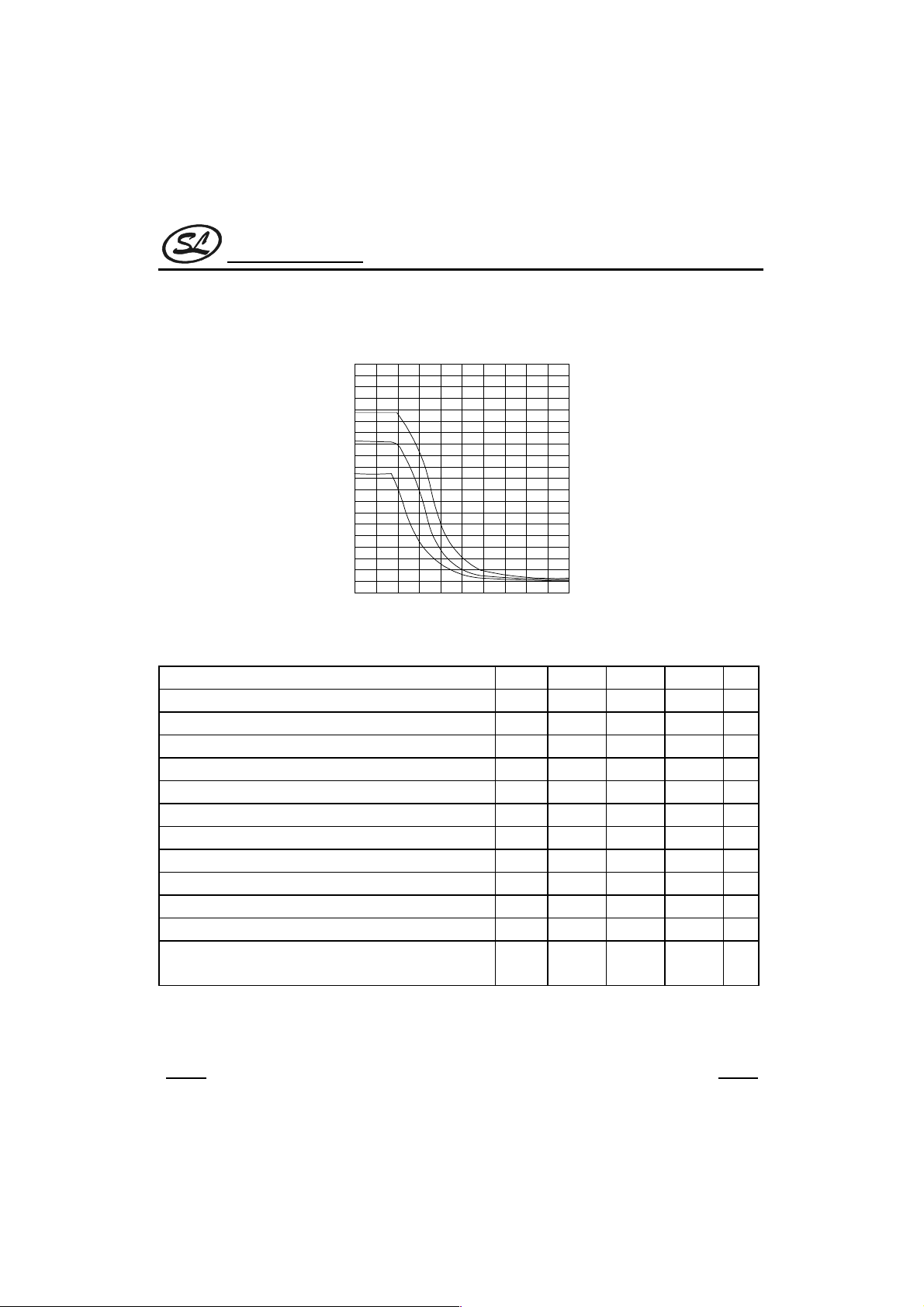
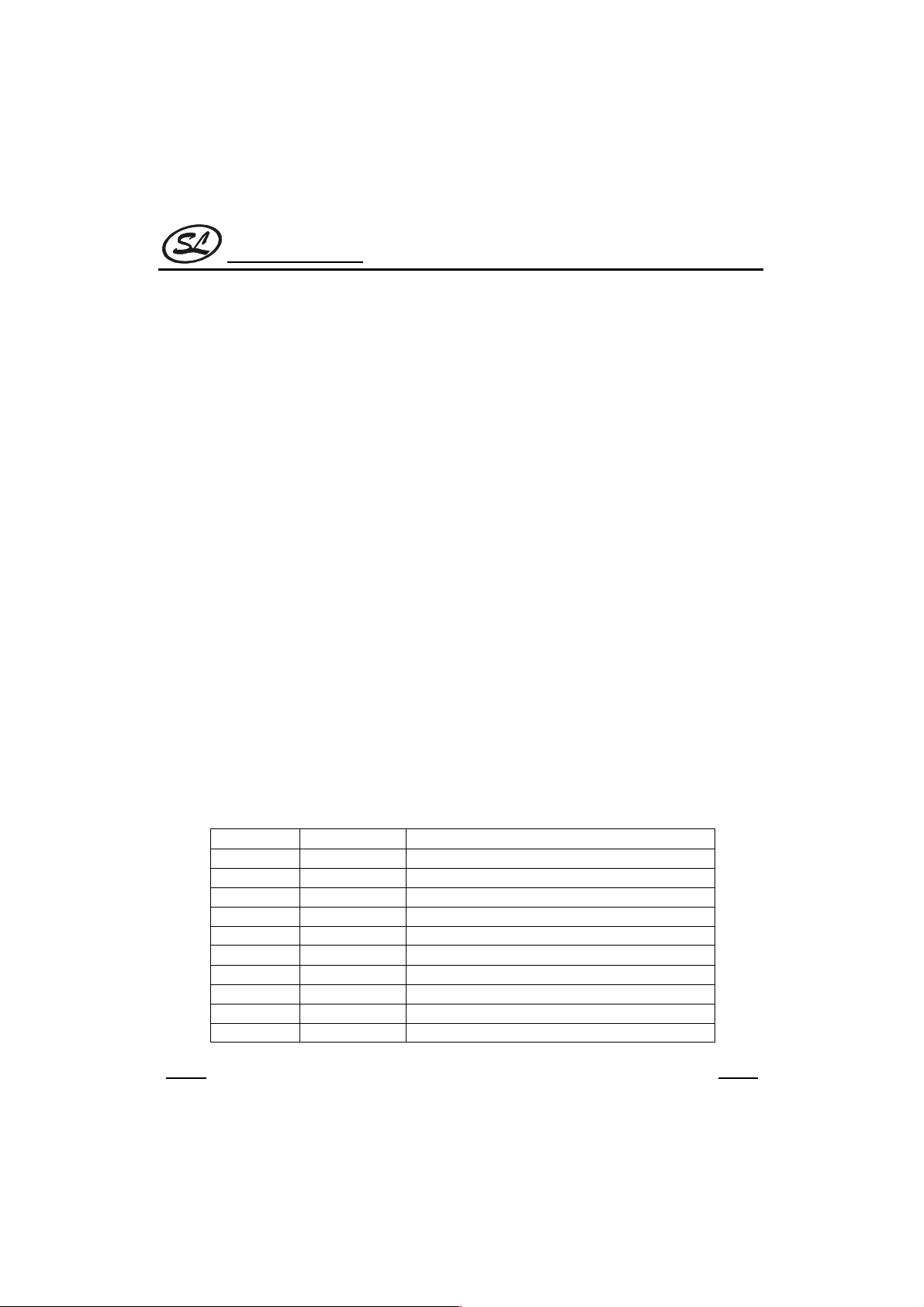
X1, X2, Y1, Y2 input impedance
UNIT:K
¡
MAX.
16.0
15.0
14.0
TYP.
13.0
12.0
MIN.
11.0
10.0
9.0
8.0
7.0
6.0
5.0
4.0
3.0
2.0
1.0
0 1.0 2.0 3.0 4.0 5.0
10.0M
VOLTAGE (LIN)
SC84510
AC ELECTRICAL CHARACTERISTICS
(Tamb=25~70°C)
Parameter Symbol Min Typ Max Unit
Oscillating Frequency Fosc 34.3-10% 34.3 34.3+10% kHz
Key Debounce Tkd -- 12 -- ms
Rising Edge Crossed Width Fosc=35KHz Tr 14.3 -- -- µs
Falling Edge Crossed Width Tf 14.3 -- -- µs
Mouse CLK Active Time Tmca -- 42.9 -- µs
Mouse CLK Inactive Time Tmci -- 42.9 -- µs
Mouse Sample DATA from CLK rising Edge Tmdc -- 14.3 -- µs
System CLK Active Time Tsca -- 42.9 -- µs
System CLK Inactive Time Tsci -- 42.9 -- µs
Time from DATA Transition to Falling Edge of CLK Tsdc -- 14.3 -- µs
Time from rising Edge of CLK to DATA Transition Tscd -- 28.6 -- µs
Time to mouse Inhibit after the 11th CLK to ensure mouse does
not start another Transmission
Tpi 0 -- 50 µs
The AC timings are measured under using 35KHz system clock signal.
HANGZHOU SILAN MICROELECTRONICS JOINT-STOCK CO.,LTD
Rev: 1.0 2000.12.31
4
Silan
Semiconductors
PIN DESCRIPTION
Pin Name I/O Description
OPT I/O
OSC OUT O
OSCR I
CLK I/O Connect to 8042 auxiliary port CLK line.
DATA I/O Connect to 8042 auxiliary port DATA line.
R
M
L
X1
I
INPUT: 200kΩ pull low to V
When OPT is connected to V
be the output of X1, while M will be the output of X2. Toggling R key can change
these output to be Y1, Y2 or Z1, Z2 respectively.
OUTPUT: 2kHz Z-axis LED-driving source.
“1” = V
High duty is about 60µs.
RC mode oscillation with 50kΩ resistor.
Three key-switches inputs.
200kΩ resistor pull low.
, “0” = floating
DD
.
SS
, SC84510 will enter test mode. In test mode, L will
DD
SC84510
X2
Y1
Y2
Z1
Z2
V
SS
V
DD
Three step dynamic input impedance.
I
Use current comparator to measure photo-couples “ON”, or “OFF”.
Z-axis input.
Photo mode: Three steps dynamic input impedance. Current comparator input.
I
Key mode: 200kΩ resistor pull low. 7 levels increased by “M” key.
Voltage mode: 200kΩ resistor pull low. 7 levels voltage comparator.
Mechanical mode: 13.2kΩ resistor pull low.
Negative power.
Power line.
HANGZHOU SILAN MICROELECTRONICS JOINT-STOCK CO.,LTD
Rev: 1.0 2000.12.31
5
Silan
Semiconductors
FUNCTION DESCRIPTIONS
1. LEGACY PS/2 MOUSE OPERATING
(A) Operating mode
There are four operating modes in PS/2 mouse:
(a) Reset Mode:
In this mode a self-test is initiated during power-on or by a Reset command. After reset signal, PS/2 mouse
will send:
a Completion code AA & ID code 00.
b Set default:
* sampling rate: 100 reports/s
* non-autospeed
* stream mode
* 2 dot/count
* disable
(b) Stream Mode:
The maximum rate of transfer is the programmed sample rate.
Data report is transmitted if
aswitchispressed
b movement has been detect
(c) Remote Mode:
Data is transmitted only in response to a Read Data command.
(d) Wrap Mode:
Any byte of data sent by the system, except hex EC (Reset wrap mode) or hex FF (Reset), is returned by
SC84510.
SC84510
(B) PS/2 Mouse Data Report:
(a) In stream mode: A data report is sent at the end of a sample interval.
(b) In remote mode: A data report is sent in response to Read Data command.
(c) Data report format:
Byte Bit Description
1 0 Left button status; 1 = pressed
1 Right button status; 1 = pressed
2 Middle button status; 1 = pressed
3 Reserve
4 X data sign; 1 = negative
5 Y data sign; 1 = negative
6 X data overflow; 1 = overflow
7 Y data overflow; 1 = overflow
2 0~7 X data (D0~D7)
3 0~7 Y data (D0~D7)
HANGZHOU SILAN MICROELECTRONICS JOINT-STOCK CO.,LTD
6
Rev: 1.0 2000.12.31
 Loading...