

SILAN SC83053 Datasheet
Silan
Semiconductors
KEYBOARD ENCODER
DESCRIPTION
The SC83053 is dedicated to a keyboard encoder, specially
designed for IBM PC AT and all compatible machines. The
SC83053 control all scan codes, three LEDs status, scan timing
and communications between the keyboard and PC. It is easy to
implement a high performance, low cost keyboard with the minimal
external components.
FEATURES
• Low cost - eliminate need external components.
• Phantom key detects.
• RC oscillator (1.8432MHz ).
• Support scan code set 1, 2 and 3.
• Support PC AT and PS/2 keyboard.
• Low power CMOS device technology.
• Internal pull-up resistor.
• Tri-state outputs for easy board application.
• Built-in 4K ROM.
• Support WINDOWS
• 104/107 keys with multi-media or other special application
keyboard encoder.
• WINDOWS is registered trademarks of Microsoft corperation.
TM
95, 98, 2000 keys.
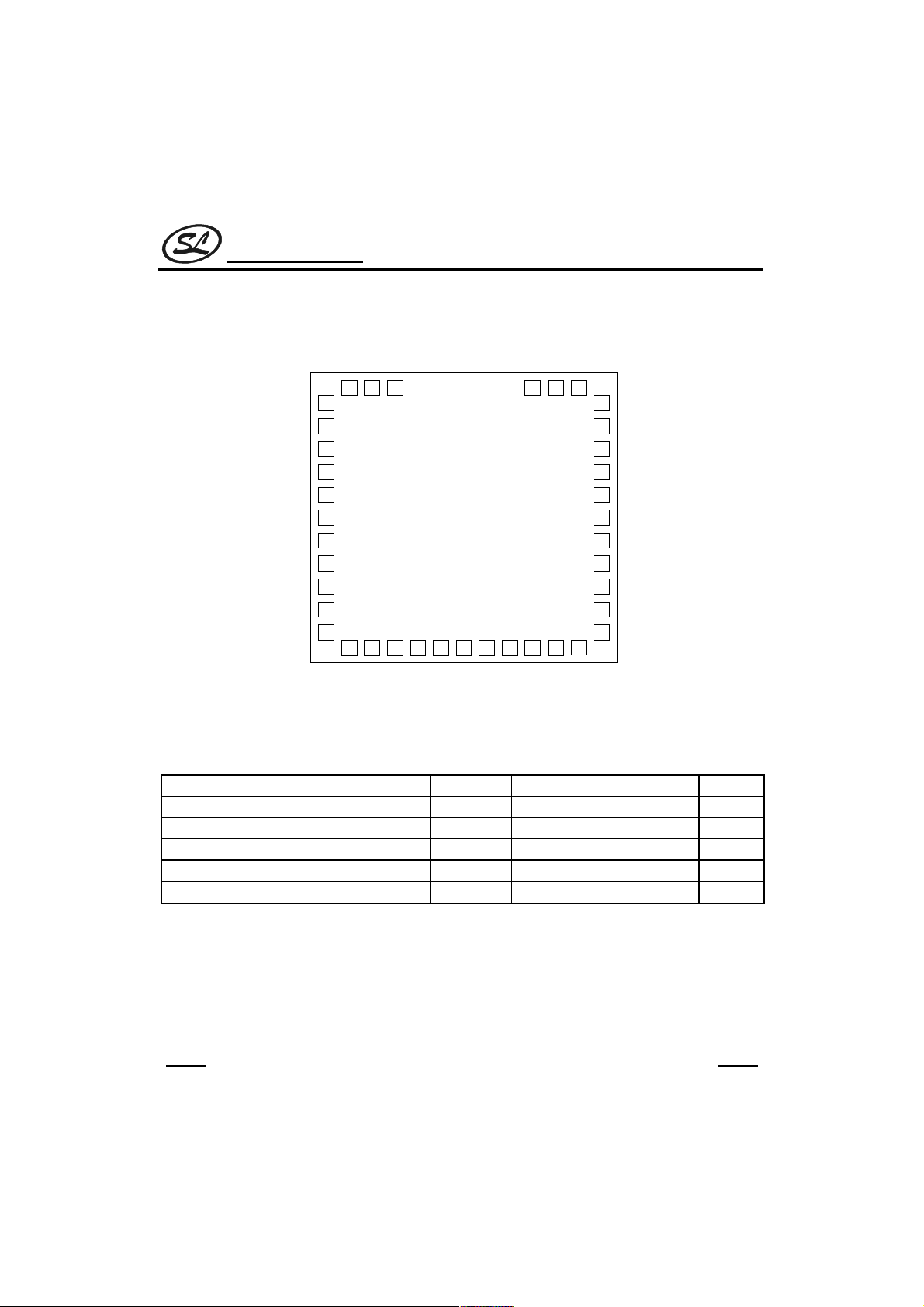
SC83053
34
5
6
7
8
9
10
11
12
13
14
15
16 17 1819 20 21 2223 24 25 26
APPLICATION
• IBM PC AT or compatible machine
keyboard.
• IBM PS/2 model 30,50,60,80 or
compatible machine keyboard.
• Japanese keyboard.
• Korean keyboard.
• Brazilian keyboard.
• European keyboard.
12
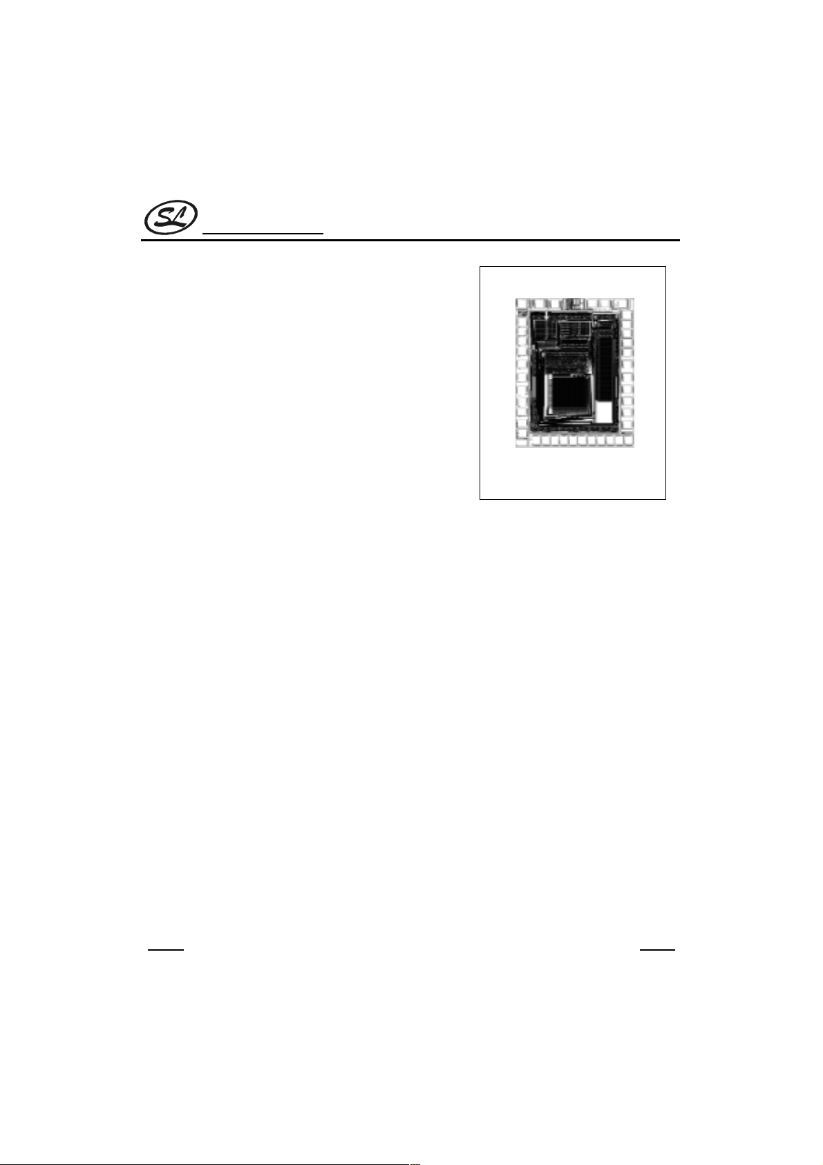
Chip Topography
3839
37
36
35
34
33
32
31
30
29
28
27
HANGZHOU SILAN MICROELECTRONICS JOINT-STOCK CO.,LTD
1
Rev: 1.0 2001.11.8.
Silan
Semiconductors
PIN CONFIGURATION
SC83053
DD
GND
V
OSCI
383923
37
P70
36
P71
35
P72
34
P67
33
P66
32
P65
31
P64
P63
30
29
P62
28
P61
P60
27
26
P85
P86
P87
P90
P91
P92
P93
P94
P95
P50
P51
P52
P53
P54
CLK
DATA
OSCO
4
5
6
7
8
9
10
11
12
13
14
161517 18 19 20 21 22 23 24 25
P55
P56
P57
SC83053
P80
P81
P82
P83
1
P84
ABSOLUTE MAXIMUM RATINGS
Characteristic Symbol Value Unit
Supply Voltage VCC -0.5~+7 V
Input Voltage VIN -0.3~+6 V
Output Voltage V
Temperature under Bias TB 0~70
Storage Temperature TS -65~150
(Ta=25°C)
-0.3~+6 V
OUT
°C
°C
HANGZHOU SILAN MICROELECTRONICS JOINT-STOCK CO.,LTD
2
Rev: 1.0 2001.11.8.
Silan
Semiconductors
DC ELECTRICAL CHARACTERISTICS
Parameter Symbol Test condition Min. Typ. Max. Unit
Operating Voltage VCC 4.5 5 5.5 V
Operating Supply Current I
Input Leakage IIN VIN=VCC, VSS
Input High Voltage VIH 2.0 V
Input Low Voltage VIL 0.8 V
Output Low Voltage V
Output Low Voltage for LEDS V
Internal Pull-high Resistance (port 6,9) RPH1 V
Internal Pull-high Resistance for
DATA, CLK
Output Low Voltage for DATA CLK V
CC1
OL1 IOL1
OL2 IOL2
RPH2 V
OL3
F
=1.8432MHz 3 mA
OSC
=3.0mA 0.4 V
=10mA 3.2 V
=0V 12 23
PH1
=0V 1.5 2.2 3
PH2
IOL3=5mA 0.4 V
AC ELECTRICAL CHARACTERISTICS
Parameter Symbol Min. Typ. Max. Unit
Time from DATA transition to falling edge of CLK T1 5 25
Time from rising edge of CLK to DATA transition T2 5 T4-5
Duration of CLK inactive T3 30 40 50
Duration of CLK active T4 30 40 50
Time to auxiliary device inhibit after clock 11 to ensure the
auxiliary device does not start another transmission
Time from inactive to active CLK transition, used to time when
auxiliary device samples DATA
System clock FCLK 1.8432 MHz
T5 50
T6 5 25
SC83053
±1 µA
KΩ
KΩ
µs
µs
µs
µs
µs
µs
PIN DESCRIPTION
Pin no. Symbol I/O Function
11 P50 O Column 3 low output scan line, 3-state
12 P51 O Column 4 low output scan line, 3-state
(To be continued)
HANGZHOU SILAN MICROELECTRONICS JOINT-STOCK CO.,LTD
3
Rev: 1.0 2001.11.8.
Silan
Semiconductors
(Continued)
Pin no. Symbol I/O Function
7-10 P92-P95 O Low output scan line, 3-state
13 P52 O Column 5 low output scan line, 3-state
14 P53 O Column 6 low output scan line, 3-state
15 P54 O Column 7 low output scan line, 3-state
16 P55 O Column 14 low output scan line, 3-state
17 P56 O Column 13 low output scan line, 3-state
18 P57 O Column 12 low output scan line, 3-state
19 P80 O Column 11 low output scan line, 3-state
20 P81 O Column 15 low output scan line, 3-state
21 P82 O Column 10 low output scan line, 3-state
22 P83 O Column 8 low output scan line, 3-state
23 P84 O Column 9 low output scan line, 3-state
24 P85 O Column 0 low output scan line, 3-state
25 P86 O Column 16 low output scan line, 3-state
26 P87 O Column 17 low output scan line, 3-state
5 P90 O Column 1 low output scan line, 3-state
6 P91 O Column 2 low output scan line, 3-state
1 GND I Ground
35 SCROLL O Scroll lock indicator
36 NUM O NUM lock indicator
37 CAPS O Caps lock indicator
27 P60 I
28 P61 I
29 P62 I
30 P63 I
31 P64 I
32 P65 I
33 P66 I
34 P67 I
4 CLK I/O
3 DATA I/O
38 VDD I +5V power supply
2 OSCO O CLOCK output
39 R_OSCI I
40 NC
Row 0 input scan line, internal pull high (17KΩ)
Row 1 input scan line, internal pull high (17KΩ)
Row 2 input scan line, internal pull high (17KΩ)
Row 3 input scan line, internal pull high (17KΩ)
Row 4 input scan line, internal pull high (17KΩ)
Row 5 input scan line, internal pull high (17KΩ)
Row 6 input scan line, internal pull high (17KΩ)
Row 7 input scan line, internal pull high (17KΩ)
CLOCK line for IBM communication, internal pull high (2.2KΩ)
DATA line for IBM communication, internal pull high (2.2KΩ)
Connect 51KΩ resistor for 1.8432MHz oscillation.
SC83053
HANGZHOU SILAN MICROELECTRONICS JOINT-STOCK CO.,LTD
4
Rev: 1.0 2001.11.8.

Silan
Semiconductors
FUNCTION DESCRIPTION
Keyboard buffer
The keyboard will buffer 16 bytes in a first-in-first-out order when the system is able to receive scan codes from
the keyboard. The response codes and repeated codes will not be buffered. If keystrokes generate a multiple-
byte sequence, the entire sequence must fit into the buffer or the keystroke is discarded and a buffer-overrun
condition occurs.
Power-on Reset and self test
The duration of the keyboard Power-on-Reset(POR) should be within 150 milliseconds and 2 seconds after the
power is applied to the keyboard.
After executing POR , the keyboard executes a self test. The LEDs are turned on at the beginning and off at
the end of the self test. The self test takes a minimum 300 milliseconds and a maximum 500 milliseconds. If the
self test is successful, a completion code AA hex is sent to the system and the keyboard starts scanning. If the
self test fails, and error code is sent, the keyboard is disabled and waits for a command from the system. The
completion codes are sent between 450 milliseconds and 2.5 seconds after POR, and between 300 and 500
milliseconds after a RESET command is acknowledged.
Keyboard data output
When the keyboard is ready to send data to the system, it first checks clock and data lines. If either one is in
the low state, data is stored in the keyboard buffer. If both are in the high state, keyboard starts clocking data out.
Data will be valid before the trailing edge and after the leading edge of the clock pulse. During the transmission
the keyboard checks the clock line at least every 60 microseconds . If the system lowers the clock lines before
the leading edge of the 10th clock, the keyboard should stop sending, then buffer the data and return clock and
data lines to high state.
Keyboard data input
When the system is ready to send data to the keyboard, it first checks clock line to see if keyboard is sending
data. If keyboard is not sending data or it is sending data but has not reached the 10th clock, the system can
inhibit the interface by forcing the clock line low for more than 60 microseconds and prepares to send data. The
keyboard checks clock line status at least every 5 milliseconds. If a system Request to Send (RTS) is detected,
the keyboard clocks 11 bits in. After the 10th bit, the keyboard checks for a high state in data line then pulls it low
and clocks one more bit to signal the system that data has been received. If data is low after the 10th bit, it
indicates a frame error. The keyboard should continue to count until data line goes high, then pulls it low and
issues a RESEND to the system
.
SC83053
HANGZHOU SILAN MICROELECTRONICS JOINT-STOCK CO.,LTD
5
Rev: 1.0 2001.11.8.

Silan
Semiconductors
Command from the system
The system can send commands to the keyboard at any time. The keyboard needs to respond within 20
milliseconds, unless the system prevents keyboard output, when doing self test or executing a RESET.
The following are the keyboard input commands and the actions that keyboard needs to take.
Set /Reset Status indicators ( Hex ED )
- Responds ACK.
- Receives option byte.
- Responds ACK.
- Updates status indicators.
- Returns to previous scanning state.
Echo ( Hex EEH )
- Responds with EE hex.
- Returns to previous scanning state.
Invalid commands ( Hex EF and F1 )
- Returns a RESEND command.
- Returns to previous scanning state.
Select Alternate Scan Codes ( Hex F0 )
- Responds ACK.
- Clears output buffer.
- Sets the default typematic rate/delay.
- Clears last typematic key.
- Receives option byte.
- Responds ACK.
- Option byte =
01 : selects scan code set 1
02 : selects scan code set 2
SC83053
HANGZHOU SILAN MICROELECTRONICS JOINT-STOCK CO.,LTD
6
Rev: 1.0 2001.11.8.

Silan
Semiconductors
03 : selects scan code set 3
- Returns to previous scanning rate.
Read ID (F2)
- Responds with ACK.
- Discontinues scanning.
- Sends two ID bytes. The second byte will be sent within 500 uS after first byte.
- Resumes scanning.
Set Typematic Rate/Delay ( Hex F3 )
- Responds ACK.
- Receives rate/delay value byte
- Responds ACK.
- Set rate/delay (* Note 1)
- Returns to previous scanning state.
* Note 1
1. Repeat period = ( 8+A ) x ( 2B) x 0.00417 seconds
A : binary value of bits 2, 1, and 0.
B : binary value of bits 4 and 3.
2. Delay = ( C +1 ) x 250 milliseconds
C : binary value of bits 6 and 5. Bit 7 is always 0.
SC83053
HANGZHOU SILAN MICROELECTRONICS JOINT-STOCK CO.,LTD
7
Rev: 1.0 2001.11.8.
Silan
Semiconductors
bit4~bit0
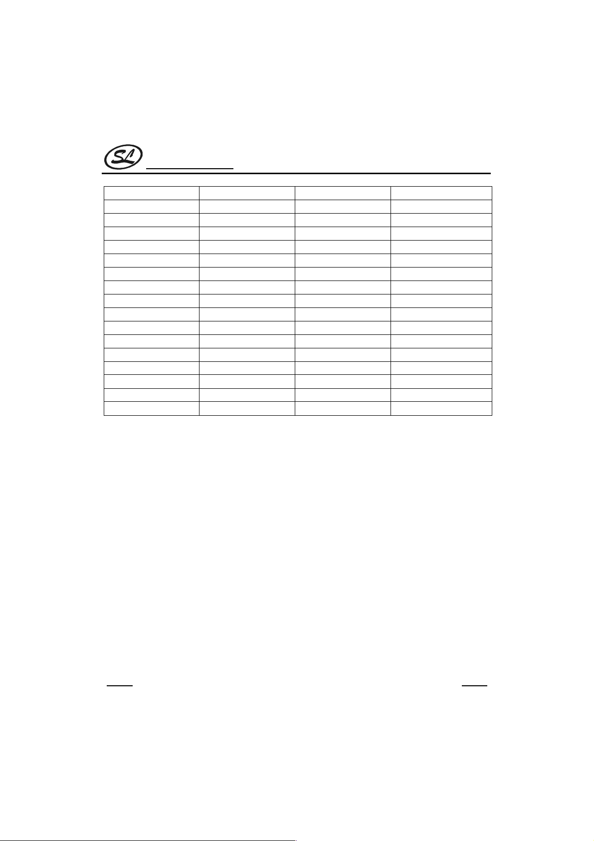
00000 30.0 10000 7.5
00001 26.7 10001 6.7
00010 24.0 10010 6.0
00011 21.8 10011 5.5
00100 20.0 10100 5.0
00101 18.5 10101 4.6
00110 17.1 10110 4.3
00111 16.0 10111 4.0
01000 15.0 11000 3.7
01001 13.3 11001 3.3
01010 12.0 11010 3.0
01011 10.9 11011 2.7
01100 10.0 11100 2.5
01101 9.2 11101 2.3
01110 8.6 11110 2.1
01111 8.0 11111 2.0
3. Default rate = 10.9 chars/sec + 20%
Default delay = 500 ms± 20%
Enable ( Hex F4 )
- Responds with ACK.
- Clears output buffer.
- Clears last typematic key.
- Start scanning.
Default Disable (Hex F5)
- Responds with ACK.
- Resets all conditions to power-on state.
- Clears output buffer.
- Sets the default key type ( scan code set 3 only ).
- Set the default typematic rate/delay.
Typematic rate ±20%
Bit 4~bit0
SC83053
Typematic rate ±20%
HANGZHOU SILAN MICROELECTRONICS JOINT-STOCK CO.,LTD
8
Rev: 1.0 2001.11.8.

Silan
Semiconductors
- Clears last typematic key.
- Stops scanning,
Set Default (Hex F6 )
- Responds with ACK.
- Resets all conditions to power-on state.
- Clears output buffer.
- Sets the default key type ( scan code set 3 only ).
- Set the default typematic rate/delay.
- Clears last typematic key.
- Continues scanning,
Set All Keys ( Hex F7,F8,F9,FA )
- Responds ACK.
- Clears output buffer.
- Sets all key type (affect only scan code set 3 operation).
F7 : Typematic
F8 : Make/Break
F9 : Make
FA : Typematic/Make/Break
- Returns to previous scanning rate.
Set Key Type ( Hex FB,FC,FD )
- Responds ACK.
- Clears output buffer.
- Receives key ID byte
- Responds ACK.
- Sets key ID type (affect only scan code set 3 operation).
FB : Typematic
FC : Make/Break
FD : Make
- Returns to previous scanning rate.
SC83053
HANGZHOU SILAN MICROELECTRONICS JOINT-STOCK CO.,LTD
9
Rev: 1.0 2001.11.8.
 Loading...