

Silan
Semiconductors
1/3 DUTY GENERAL-PURPOSE LCD
DRIVER
DESCRIPTION
The SC75823 is a general-purpose LCD driver that can be used
for frequency display in microprocessor-controlled radio receives
and in other display applications. In addition to being able to directly
drive up to 156 LCD segments.
FEATURES
• Supports both 1/3 duty 1/2 bias and 1/3 duty 1/3 bias LCD
drive of up to 156 segments under serial data control.
• Serial data input supports CCB format communication with the
system controller.
• Serial data control of the power-saving mode based backup
function and all the segments forced off function.
• High generality since display data is displayed directly without
decoder intervention.
• The
INH pin can force the display to the off state.
• The LCD drive bias voltage can be provided internally or
externally.
• Power supply voltage: 4.5 to 6.0V
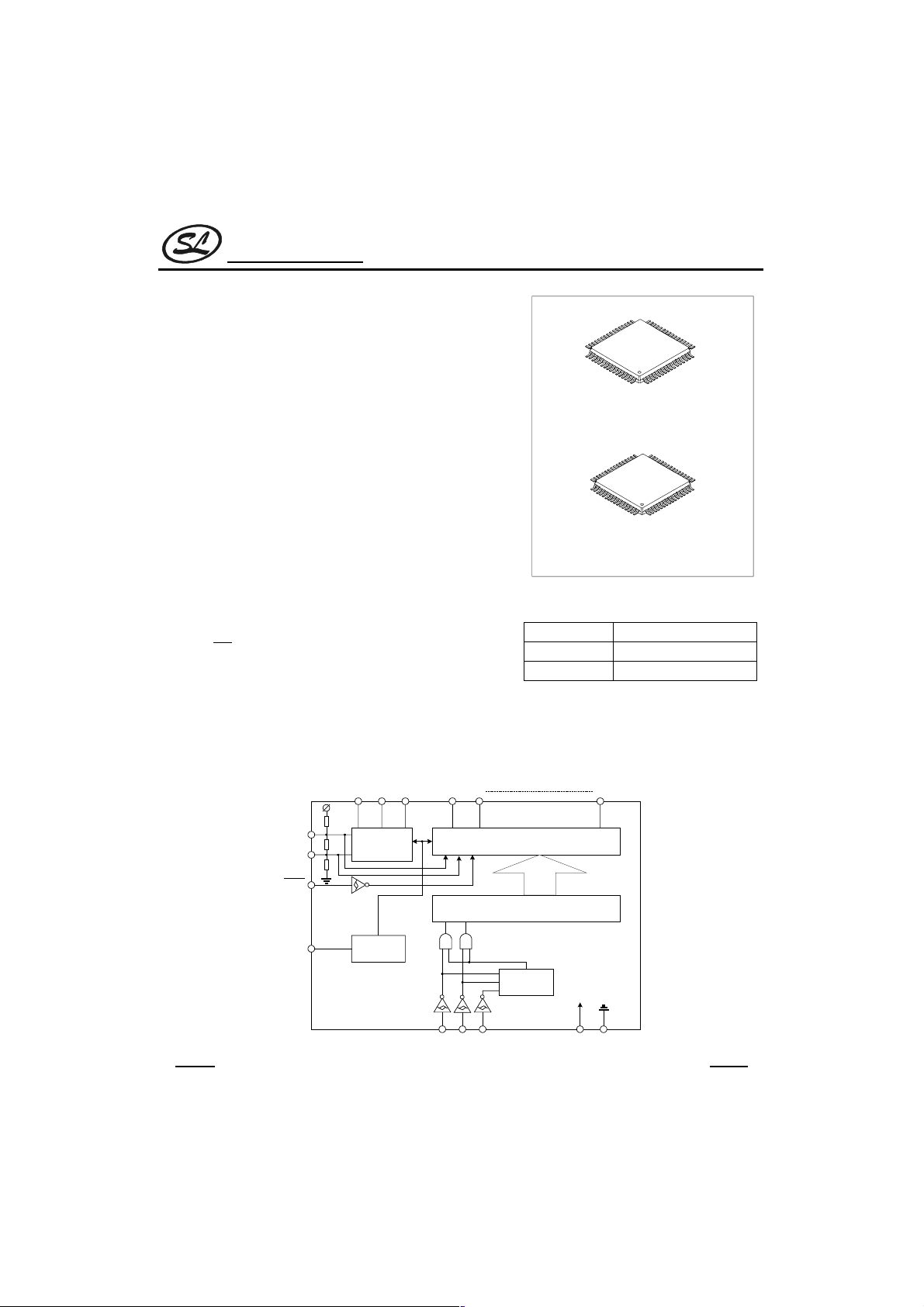
BLOCK DIAGRAM
SC75823
QFP-64-14x14-0.8
LQFP-64-10 x 10-0.5
ORDERING INFORMATION
Device Package
SC75823A LQFP-64-10 X 10-0.5
SC75823B QFP-64-14 X 14-0.8
S1S51S52COM1 COM2 COM3
V
V
INH
OSC
DD1
DD2
Common Driver
Clock
Generator
DI CL CE
Latch & Driver
Shift Register
Address
Detector
V
DDVSS
HANGZHOU SILAN MICROELECTRONICS JOINT-STOCK CO.,LTD
1
Rev: 1.1 2002.03.04
Silan
Semiconductors
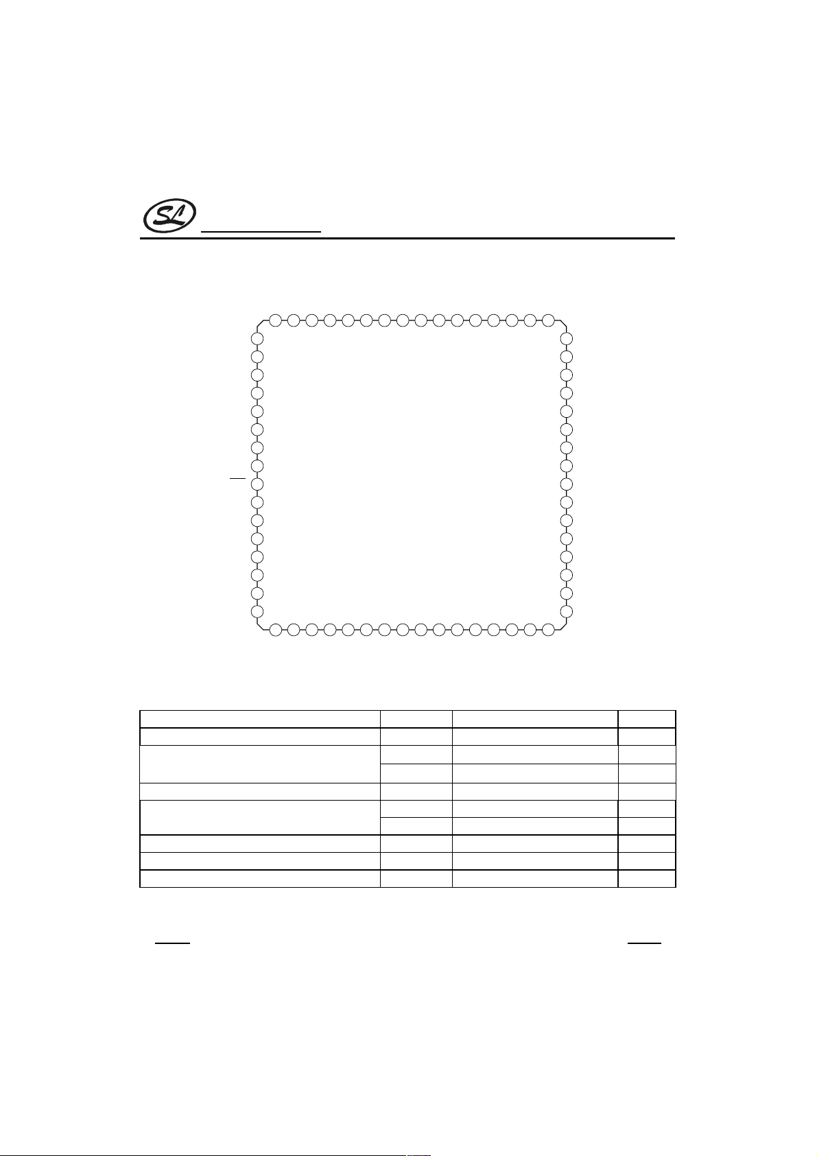
PIN CONFIGURATION
S48
48 47 46 45 44 43 42 41 40 39 38 37
49
S49
50
S50
51
S51
52
S52
53
COM1
54
COM2
55
COM3
56
DD
V
57
INH
58
DD1
V
59
V
DD2
V
60
SS
61
OSC
62
CE
63
CL
64
DI
1
S1
S34
S35
S36
S37
S38
S39
S40
S41
S42
S43
S44
S45
S46
S47
36 35 34 33
SC75823
2 3 4 5 6 7 8 9 10 11 12 13 14 15 16
S2
S4
S3
S5S6S7S8S9
S10
S11
S12
S13
S14
S15
SC75823
S33
S32
32
S31
31
S30
30
S29
29
S28
28
S27
27
S26
26
S25
25
S24
24
S23
23
S22
22
S21
21
S20
20
19
S19
18
S18
S17
17
S16
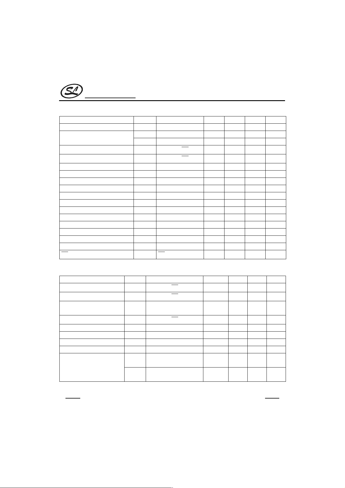
ABSOLUTE MAXIMUM RATINGS
Characteristics Symbol Value Unit
Maximum Supply Voltage V
Input Voltage
Output Voltage V
Output Current
Allowable Power Dissipation P
Operating Temperature T
Storage Temperature T
(Tamb=25°C, VSS=0 V)
HANGZHOU SILAN MICROELECTRONICS JOINT-STOCK CO.,LTD
-0.3 to +6.5 V
DDmax
V
-0.3 to +6.5 V
IN1
-0.3 to VDD+0.3 V
V
IN2
-0.3 to VDD+0.3 V
OUT
I
300
OUT1
3 mA
I
OUT2
200 mW
Dmax
-40 to +85
opr
-55 to 125
stg
µA
°C
°C
2
Rev: 1.1 2002.03.04
Silan
Semiconductors
ALLOWABLE OPERATING RANGE
Characteristics Symbol Test Condition Min. Typ. Max. Unit
Supply Voltage VDD VDD 4.5 6.0 V
Input Voltage
Input High level Voltage VIH
Input Low Level Voltage VIL
Recommended External Resistance R
Recommended External Capacitance C
Guaranteed Oscillator Range f
Data Setup Time tds CL, DI: figure 2 100 ns
Data Hold Time tdh CL, DI: figure 2 100 ns
CE Wait Time tcp CE, CL: figure 2 100 ns
CE Setup Time tcs CE, CL: figure 2 100 ns
CE Hold Time tch CE, CL: figure 2 100 ns
High-level Clock Pulse Width
Low-level Clock Pulse Width
Rise Time tr CE, CL, DI: figure 2 100 ns
Fall Time tf CE, CL, DI: figure 2 100 ns
Switching Time
INH
V
V
(Tamb=-40 to +85°C, VSS=0V)
V
DD1
DD2
OSC
OSC
OSC 19 38 76 kHz
OSC
tφH
tφL
t2
2/3VDD 6.0 V
DD1
V
1/3VDD 6.0 V
DD2
CE, CL, DI,
CE, CL, DI,
OSC 47
OSC 1000 pF
CL: figure 2 100 ns
CL: figure 2 100 ns
, CE: figure 3
INH
INH
INH
4.0 6.0 V
0 0.7 V
10
SC75823
kΩ
µs
ELECTRICAL CHARACTERISTICS
Characteristics Symbol Test Condition Min. Typ. Max. Unit
Input High Level Current IIH
Input Low Level Current IIL
Oscillator Frequency f
Hysteresis Width VH
Output High Level Voltage V
Output Low Level Voltage V
Output High Level Voltage V
Output Low Level Voltage V
Intermediate Level Voltage
V
V
OSC
OH1
OL1
OH2
OL2
MID1
MID2
CE, CL, DI,
CE, CL, DI,
OSC;R
OSC
C
=1000pF
OSC
CE, CL, DI,
S1 to S52; I
S1 to S52; I
COM1 to COM3; I
COM1 to COM3; I
1/2 bias, COM1 to COM3;
I
=±100µA
O
1/3 bias, COM1 to COM3;
I
=±100µA
O
INH
INH
=47kΩ,
INH
=-20µA
O
=20µA
O
; VI=6V
; VI=0V
; VDD=5V
=-100µA
O
=100µA
O
5
-5
38 kHz
0.3 V
-1.0 V
V
DD
1.0 V
-1.0 V
V
DD
1.0 V
±1.0
1/2V
2/3V
DD
DD
±1.0
V
V
(To be continued)
µA
µA
HANGZHOU SILAN MICROELECTRONICS JOINT-STOCK CO.,LTD
3
Rev: 1.1 2002.03.04
Silan
Semiconductors
(Continued)
Characteristics Symbol Test Condition Min. Typ. Max. Unit
V
Intermediate Level Voltage*
Supply Current
Note: * Except the bias voltage generation divider resistors that are built into V
V
V
1/3 bias, COM1 to COM3;
MID3
I
=±100µA
O
1/3 bias, S1 to S52;
MID4
I
=±20µA
O
1/3 bias, S1 to S52;
MID5
I
=±20µA
O
I
Power saving mode 5
DD1
I
f=38kHz, 1/2 bias, VDD=5V 400 800
DD2
I
f=38kHz, 1/3 bias, VDD=5V 300 600
DD3
I
f=38kHz, 1/2 bias, VDD=6V 650 1300
DD2
I
f=38kHz, 1/3 bias, VDD=8V 580 1200
DD3
Figure 1
V
DD
1/3V
2/3V
1/3V
DD
DD
DD
DD1
SC75823
±1.0
±1.0
±1.0
V
V
V
and V
.(see figure 1)
DD2
µA
µA
µA
µA
µA
V
DD1
To the common segment driver
V
DD2
Except these resistors
HANGZHOU SILAN MICROELECTRONICS JOINT-STOCK CO.,LTD
4
Rev: 1.1 2002.03.04
Silan
Semiconductors
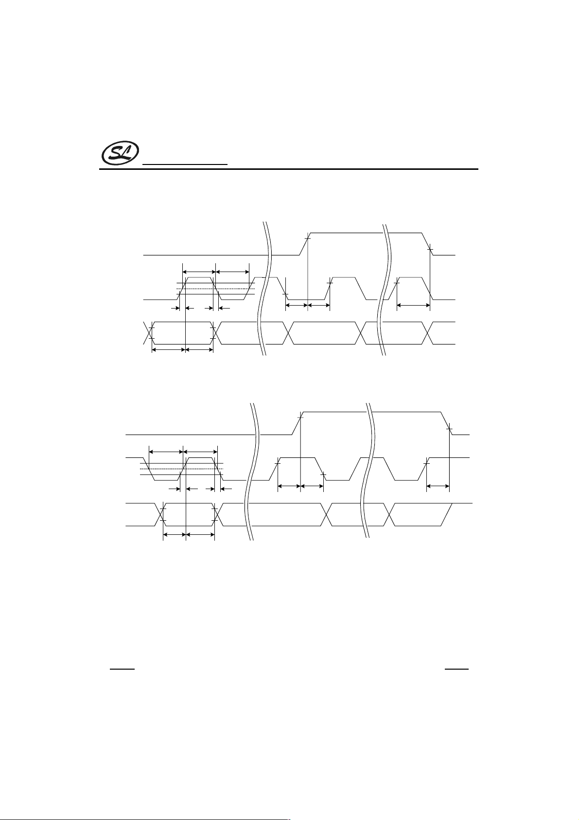
1.When CL is stopped at the low level
CE
t¶Ht¶L
CL
DI
2.When CL is stopped at the high level
CE
V
IH
50%
V
IL
V
IH
V
IL
tds tdh
tr
V
V
tf
IH
IL
SC75823
Fig 2
IH
V
V
IL
V
V
V
IL
IH
V
IH
IH
tchtcstcp
V
IL
Ht¶L
t
CL
V
IH
50%
IL
V
DI
IH
V
V
IL
tds tdh
tr tf
V
IH
V
IL
V
IH
V
IL
tcp tcs tch
V
IH
HANGZHOU SILAN MICROELECTRONICS JOINT-STOCK CO.,LTD
5
Rev: 1.1 2002.03.04
 Loading...