

SILAN SC6121-001, SC6121-002 Datasheet
Silan
Semiconductors
INFRARED REMOTE CONTROL
TRANSMITTER
DESCRIPTION
The SC6121 is a remote control transmitter utilizing CMOS
Technology specially designed for use on infrared remote control
applications. It is capable of controlling 32 function keys and 3
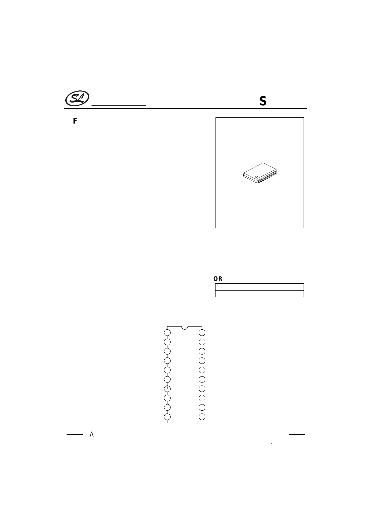
double keys. SC6121 is housed in a 20-pins SO package.
FEATURES
* CMOS Technology
* Low Operating Voltage (V
* Using SEL pin, SC6121 can support 64+6 function codes
* Customer Code can be selected
APPLICATIONS
* TV and VCR
* Audio Equipment
* Cable TV Tuner
* Cassette Deck
* Air Conditioner
* VCD and DVD ROM/Player
* Moniputer/Multi-Media Personal Computer System
PIN CONFIGURATION
=2.0~5.5V)
DD
SC6121
SOP-20
ORDERING INFORMATION
SC6121-001
SC6121-002
ROM Content=0
Custom Version
KI0
KI1
KI2
KI3
REM
V
DD
SEL
OSCO
OSCI
Vss
1
2
3
4
5
6
7
8
9
10
SC6121
CCS
20
KI/O0
19
KI/O1
18
KI/O2
17
KI/O3
16
KI/O4
15
KI/O5
14
KI/O6
13
KI/O7
12
LMP
11
HANGZHOU SILAN MICROELECTRONICS JOINT-STOCK CO.,LTD
Rev: 1.2 2002-02-28
1
Silan
Semiconductors
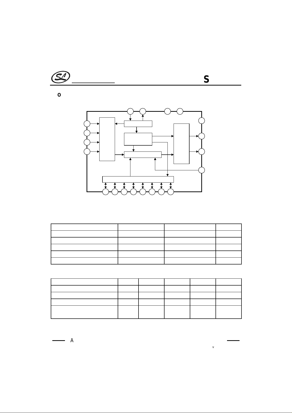
BLOCK DIAGRAM
KI0
KI1
KI2
KI3
OSCI OSCO V
89 6 10
1
2
3
Key
Input
Scan
Circuit
4
OSC Circuit
Timing Generation
&Control Circuit
Code Generation Circuit
Key Input/Output Scan Circuit
1819 1617 1415 1213
KI/O0 KI/O1 KI/O2 KI/O3 KI/O4 KI/O5 KI/O6 KI/O7
DD
Vss
Optput
Control
Circuit
ABSOLUTE MAXIMUM RATING
Characteristic Symbol Value Unit
Supply Voltage V
Input Voltage V
Power Dissipation Pd 250 mW
Storage Temperature T
Operating Temperature T
(Tamb=25°C, unless otherwise specified)
DD
IN
stg
opr
6.0 V
-0.3~VDD V
-40~+125
-20~+75
RECOMMENDED OPERATING CONDITIONS
Characteristic Symbol Min. Typ. Max. Unit
Supply Voltage V
Oscillation Frequency fosc 400 455 500 KHz
Input Voltage V
Custom Code Select Pull-Up
Resistance
DD
IN
Rup -- 100 --
(Tamb=25°C, unless otherwise specified)
2.0 3.0 3.3 V
0--VDDV
SC6121
SEL
7
REM
5
LMP
11
CSS
20
°C
°C
KΩ
HANGZHOU SILAN MICROELECTRONICS JOINT-STOCK CO.,LTD
Rev: 1.2 2002-02-28
2
Silan
Semiconductors
ELECTRICAL CHARACTERISTICS
Parameter Symbol Test conditions Min Typ Max Unit
Supply Voltage V
Current Consumption 1 I
Current Consumption 2 I
REM High Level Output Current I
REM Low Level Output Current I
LMP High Level Output Current I
LMP Low Level Output Current I
KI High Level Input Current I
KI Low Level Input Current I
KI High Level Input Voltage V
KI Low Level Input Voltage V
KI/O High Level Input Voltage V
KI/O Low Level Input Voltage V
KI/O High Level Input Current I
KI/O Low Level Input Current I
KI/O High Level Output Current I
KI/O Low Level Output Current I
CCS Low Level Input Voltage V
CCS High Level Input Current I
CCS Low Level Input Current I
CCS High Level Input Current I
CCS Low Level Input Current I
PIN DESCRIPTION
Pin No. Symbol I/O Description
1~4 KI0~KI3 I Key Input Pin Nos. 0~3
5 REM O Data Output Pin
6VDD-- Power Supply
7 SEL I Select Pin
8 OSCO O Oscillator Pin
9 OSCI I Oscillator Pin
10 Vss -- Power Supply
11 LMP -- Output LED Indicator
19~12 KI/O0~KI/O7 I/O Key Input/Output Pin Nos.0~7
20 CCS I Custom Code Scan Input Pin
DD1
DD2
OH1
OL1
OH2
OL2
OH3
OL3
IH1
IL1
IH1
IH2
IH2
IL2
IH3
IH3
IL3
IH4
IL4
(Tamb=25°C,VDD=3.0V,unless otherwise specified)
DD
Fosc =455KHz 0.1 1.0 mA
Fosc =STOP 1.0
Vo=1.5V -5.0 -8.0 mA
Vo=0.3V 15 30
Vo=2.7V -15 -30
Vo=0.3V 1 1.5 mA
VIN=3.0V 5 30
VIN=0V -0.2
IL1
IL2
VIN=3.0V 2 7
VIN=0V -0.2
Vo=2.5V 0.5 1.5 mA
Vo=1.7V 1.5 2.5 mA
Pull Up VIN=3.0V 0.2
Pull Up VIN=0V -3 -15
Pull Down VIN=3.0V 5 30
Pull Down VIN=0V -0.2
SC6121
2.0 3.0 5.5 V
µA
µA
µA
µA
µA
0.7 V
DD
00.3V
0.7 V
DD
00.4V
1.1 V
V
V
DD
DD
DD
V
V
V
µA
µA
µA
µA
µA
µA
HANGZHOU SILAN MICROELECTRONICS JOINT-STOCK CO.,LTD
Rev: 1.2 2002-02-28
3
Silan
Semiconductors
FUNCTIONAL DESCRIPTION
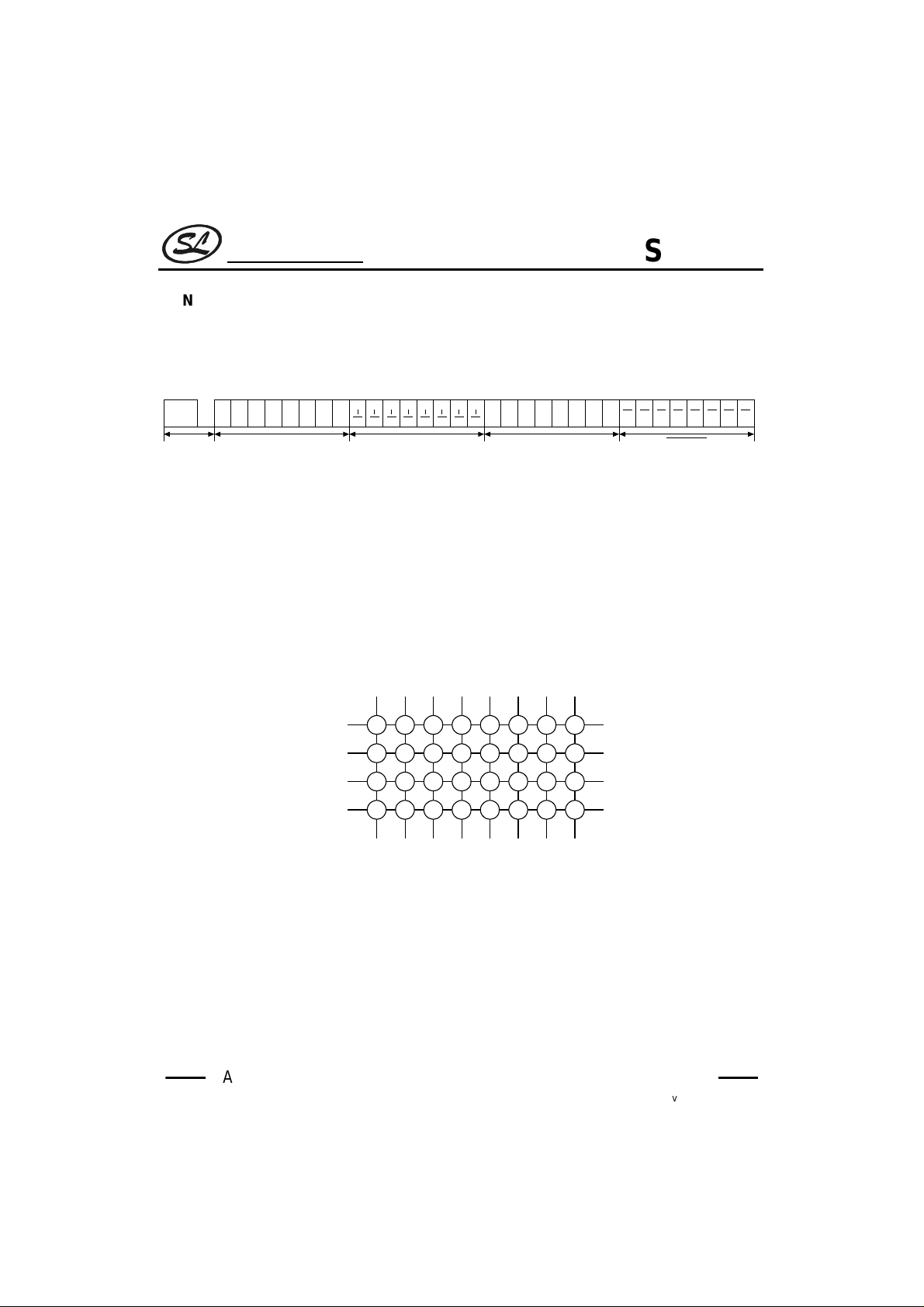
1. TRANSMISSION CODE
The transmission code consists of a leader code, 16-bits custom codes, and 8-bits data codes. The inverse
code of the data code is also sent simultaneously. The following diagram shows this one frame construction.
C0'
C0'
C0 C1 C2 C3 C5C4 C6 C7
Leader
Code
Custom Code
8bits
The leader codes consist of a 9ms carrier waveform followed by a 4.5ms OFF waveform. It is used as the leader
for the following code. Thus, when reception is configured by a microcomputer, the time relationship between the
reception detection and other processes can be managed efficiently. The code uses the PPM (Pulse Position
Modulation) Method, with "0" and "1" differentiated by the time between pulses. Each code consists of 8 bits, and
simultaneous transmission of the inverse code allows configuration of a system with an extremely low error rate.
2. KEY INPUT MATRIX
The Key Input Matrix of SC6121 if given below:
C0'C2C0'C3C0'C4C0'C5C0'C6C0'
C0
C1
Custom Code'
8bits
D0 D1 D2 D3 D4 D0 D1 D2 D3 D4 D5 D6 D7
C7
Key Data
8bits
D5 D6 D7
SC6121
Key Data
8bits
KI/O0
KI/O1
KI/O2
KI/O3
KI/O4
KI/O5
KI/O6
KI/O7
KI0
KI1
KI2
KI3
51 139 2117 2925
62 1410 2218 3026
73 1511 2319 3127
84 1612 2420 3228
3. KEY INPUT
A total of 32 keys can be connected by SC6121 Key Input Pins--KI0~KI3 and the Timing Signal Output Pins
KI/O0~KI/O7.
Double Key Operation is possible for only Key No.21 in combination with other keys connected to the KI/O5 line
namely: Key No.22,23 or 24.thus, only the following key combinations may be used for the double key operation:
1. Key Nos.21 and 22
2. Key Nos.21 and 23
3. Key Nos.21 and 24
HANGZHOU SILAN MICROELECTRONICS JOINT-STOCK CO.,LTD
Rev: 1.2 2002-02-28
4
 Loading...