

SILAN SC5262D-IR, SC5262D-RF, SC5262S-IR, SC5262S-RF Datasheet
Silan
Semiconductors
REMOTE CONTROL ENCODER
DESCRIPTION
The SC5262 is a remote control encoder paired with SC5272
utilizing CMOS technology. It encodes data and address pins into a
serial coded waveform suitable for RF or IR modulation. SC5262
has a maximum of 12-bits of tri-state address pins providing up to
531,441(or 3
code collision and unauthorized code scanning possibilities.
FEATURES
* Low power consumption and very high noise immunity
* Up to 12 tri-state code address pins or 6 data pins
* Wide operating voltage range(Vcc=3V ~ 15V)
* Single resistor oscillator
* Latch or Momentary output type
12
) address codes; thereby, drastically reducing any
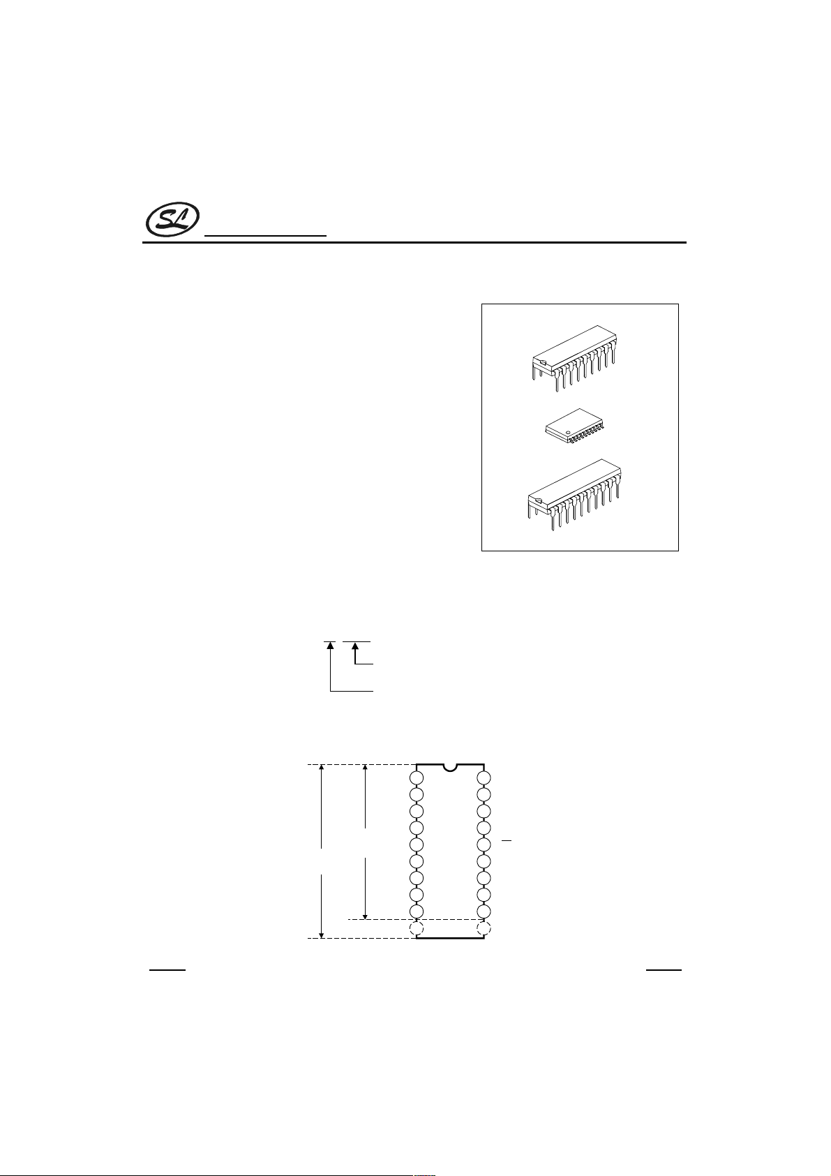
SC5262
DIP-18
SOP-20
APPLICATION
* Home/automation security system
* Remote control toys or for industrial use
* Remote control fan
* Garage door controller
ORDERING INFORMATION
SC5262X-XX
PIN CONFIGURATION
20 Pin
Package
RF: RF Applicatant, normally omitted
IR: IR Applicatant
S: SOP-20 Package
D: DIP-20 Package
Omitted: DIP-18Package
A0
1
A1
A2
A3
18 Pin
A4
Package
A5
A6/D5
A7/D4
Vss
NC
SC5262
Vcc
Dout
OSC1
OSC2
TE
A11/D0
A10/D1
A9/D2
A8/D3
NC
DIP-20
HANGZHOU SILAN MICROELECTRONICS JOINT-STOCK CO.,LTD
Rev: 1.0 2000.12.31
1
Silan
Semiconductors
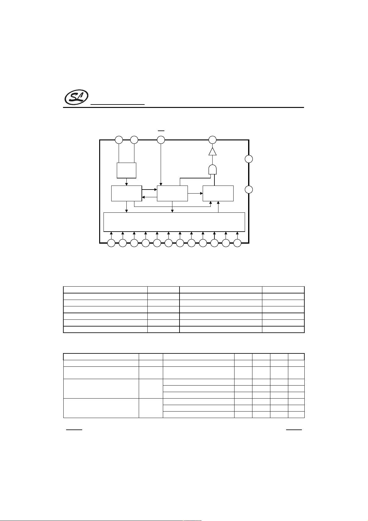
BLOCK DIAGRAM
SC5262
TE
DoutOSC1OSC2
17141615
Vcc
18
OSC
Vss
System
Timing
Control
Logic
Code
Generation
9
Address
87654321 11 12 13
10
A0 A1 A2 A3 A4 A5
The block diagram is for DIP-18(hereinafter is the same)
A6/D5A7/D4A8/D3A9/D2A10/D1A11/
D0
ABSOLUTE MAXIMUM RATINGS
Characteristic Symbol Value Unit
Supply Voltage Vcc -0.3 ~ 16.0 V
Input Voltage Vi -0.3 ~ Vcc+0.3 V
Output Voltage Vo -0.3 ~ Vcc+0.3 V
Maximum Power Dissipation(Vcc=12V) Pa 300 mW
Operating Temperature Topr -20 ~ +70
Storage Temperature Tstg -40 ~ +125
(Ta=25°C)
°C
°C
ELECTRICAL CHARACTERISTICS
(Ta=25°C,Vcc=12V,unless otherwise specified)
Characteristic Symbol Test Condition Min Typ. Max Unit
Supply Voltage Vcc 3 15 V
Supply Current
Dout Output driving Current I
Dout Output sinking Current I
Vcc=12V,OSC stops
Icc
A0~ A11 Open
Vcc=5V,VOH=3V -3 mA
Vcc=8V,VOH=4V -6 mA
OH
Vcc=12V,VOH=6V -10 mA
Vcc=5V,VOL=3V 2 mA
Vcc=8V,VOL=4V 5 mA
OL
Vcc=12V,VOL=6V 9 mA
0.02 0.3
µA
HANGZHOU SILAN MICROELECTRONICS JOINT-STOCK CO.,LTD
Rev: 1.0 2000.12.31
2
Silan
Semiconductors
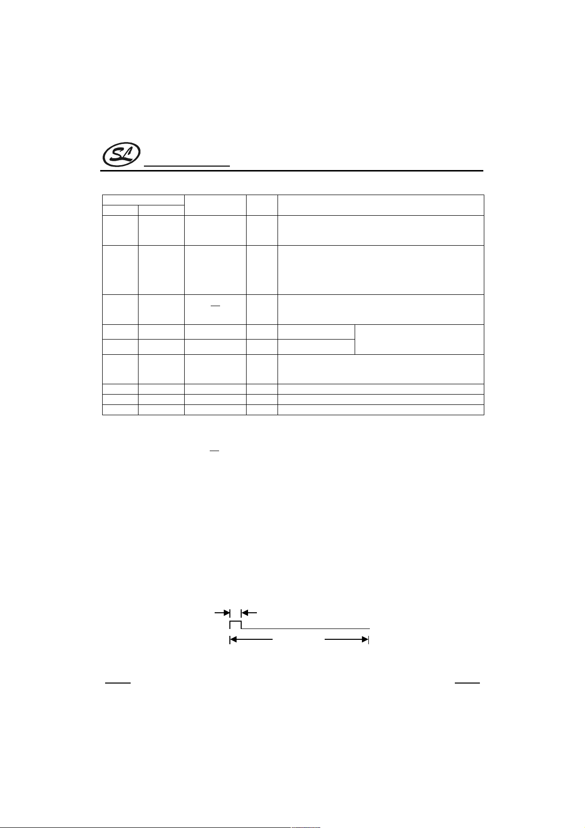
PIN DESCRIPTION
Pin No.
18 PIN 20 PIN
1~6 1~6 A0~A5 I
7~8
10~13
14 16
15 17 OSC1 O Oscillator Pin No.1
16 18 OSC2 I Oscillator Pin No.2
17 19 DOUT O
18 20 Vcc -- Positive Power Supply
9 9 Vss -- Negative Power Supply
-- 10~11 NC -- Not Connected
7~8
12~15
Pin Name I/O Description
Code Address pins No. 0~5. These six tri-state pins are
detected by SC5262 to determine the encoded waveform
bit 0 ~bit 5. Each pin can be set to “0”,”1”,”f”(floating).
Code Address pinsNo.6~11/data pins No.5~0. These six
A6/D5~A11/D0 I
TE
tri-state pins are detected by SC5262 to determine the
encoded waveform bit 6 ~bit 11.When these pins are used
as address pins, they can be set to “0”,”1”,”f”.When they
are used as data pins ,they can be set only to “0”,”1”.
Transmission Enable. Active Low Signal.SC5262 outputs
I
the encoded waveform to DOUT whenthis pins is pulled to
LOW.
A resistor connected between
these two pins determine the
fundamental frequency of SC5262.
Data Output Pin. The encoded waveform is serially
outputted to this pin. When SC5262 is not transmitting,
DOUT outputs low(Vss) voltage.
FUNCTIONAL DESCRIPTION
The SC5262 encodes the code address and data set at A0~ A5 and A6/D5 ~ A11/D0 into a special waveform
and outputs it to the Dout when
the IR transmitter for transmission. The Transmitted radio frequency or infrared ray is received by the RF
demodulator or IR receiver and reshaped to the special waveform. SC5272 is then used to decode the waveform
and set the corresponding output pins. Thus completing a remote control encoding and decoding function.
TE
is pulled to “0” (Low state). This waveform is fed to either the RF modulator or
SC5262
1. RF OPERATION
Code Bits
A code bit is the basic component of the encoded waveform, and can be classified as either an AD(Address/Data)
Bit or a SYNC(Synchronous) Bit.
An AD bit can be designated as bit “ 0 ”, “ 1 ” or “ f ” if it is in low, high or floating state respectively. One bit
waveform consists of two pulse cycles. Each pulse cycle has 16 oscillating time periods. For further details, please
refer to the diagram below:
The Synchronous bit waveform is 4 bits long with 1/8 bit width pulse. Please refer to the diagram below:
1/8 bit width=4a
4 bit width=128a
Note: 1bit =32a
HANGZHOU SILAN MICROELECTRONICS JOINT-STOCK CO.,LTD
Rev: 1.0 2000.12.31
3
 Loading...