


SF1530
High Performance Current Mode PWM Controller
FEATURES |
GENERAL DESCRIPTION |
Proprietary “Zero OCP/OPP Recovery Gap” Control
Built-in Soft Start Function
All Pins Floating Protection
Very Low Startup Current
High Voltage CMOS Process with Excellent ESD Protection
Frequency Reduction and Burst Mode Control for Energy Saving
Current Mode Control
Built-in Frequency Shuffling
Programmable Switching Frequency
Built-in Synchronous Slope Compensation
Cycle-by-Cycle Current Limiting
Built-in Leading Edge Blanking (LEB)
Constant Power Limiting
Audio Noise Free Operation
VDD OVP & Clamp
VDD Under Voltage Lockout (UVLO)
APPLICATIONS
Offline AC/DC Flyback Converter for
AC/DC Adaptors
Open-frame SMPS
Set-Top Box Power Supplies
ATX Standby Power
TYPICAL APPLICATION
SF1530 is a high performance, low cost, highly integrated current mode PWM controller for offline flyback converter applications.
PWM switching frequency with shuffling is externally programmable, which can reduce conduction EMI emission of a power supply. When the output power demands decrease, the IC automatically decreases switching frequency for high power conversion efficiency. When the current set-point falls below a given value, e.g. the output power demand diminishes, the IC enters into burst mode and provides excellent efficiency without audio noise.
The IC can achieve “Zero OCP/OPP Recovery Gap” using SiFirst’s proprietary control algorithm. Meanwhile, the OCP/OPP variation versus universal line input is compensated.
The IC has built-in synchronized slope compensation to prevent sub-harmonic oscillation at high PWM duty output. The IC also has built-in soft start function to soften the stress on the MOSFET during power on period.
SF1530 integrates functions and protections of Under Voltage Lockout (UVLO), VCC Over Voltage Protection (OVP), Cycle-by-cycle Current Limiting (OCP), All Pins Floating Protection, Over Load Protection (OLP), RT Pin Short-to-GND Protection, Gate Clamping, VCC Clamping, Leading Edge Blanking (LEB).
SF1530 is available in SOT23-6, SOP-8 and DIP-8 packages.
|
|
|
DC Out |
AC IN |
|
|
|
6 |
5 |
4 |
|
GATE |
VDD |
CS |
|
SF1530 |
|
|
|
GND |
FB |
RT |
|
1 |
2 |
3 |
|
|
|
|
TL431 |
©SiFirst Technology |
|
www.sifirsttech.com |
|
|
|
- 1 - |
SF1530_DS_V1.0 |
|
|
|
|
|
|
|
|
|
|
|
|
|
|
|
|
|
|
|
|
|
|
SF1530 |
|
||
|
|
|
|
|
|
|
|
|
|
|
|
|
|
|
|
|
|
|
|
|
|
|
|
|
|
|
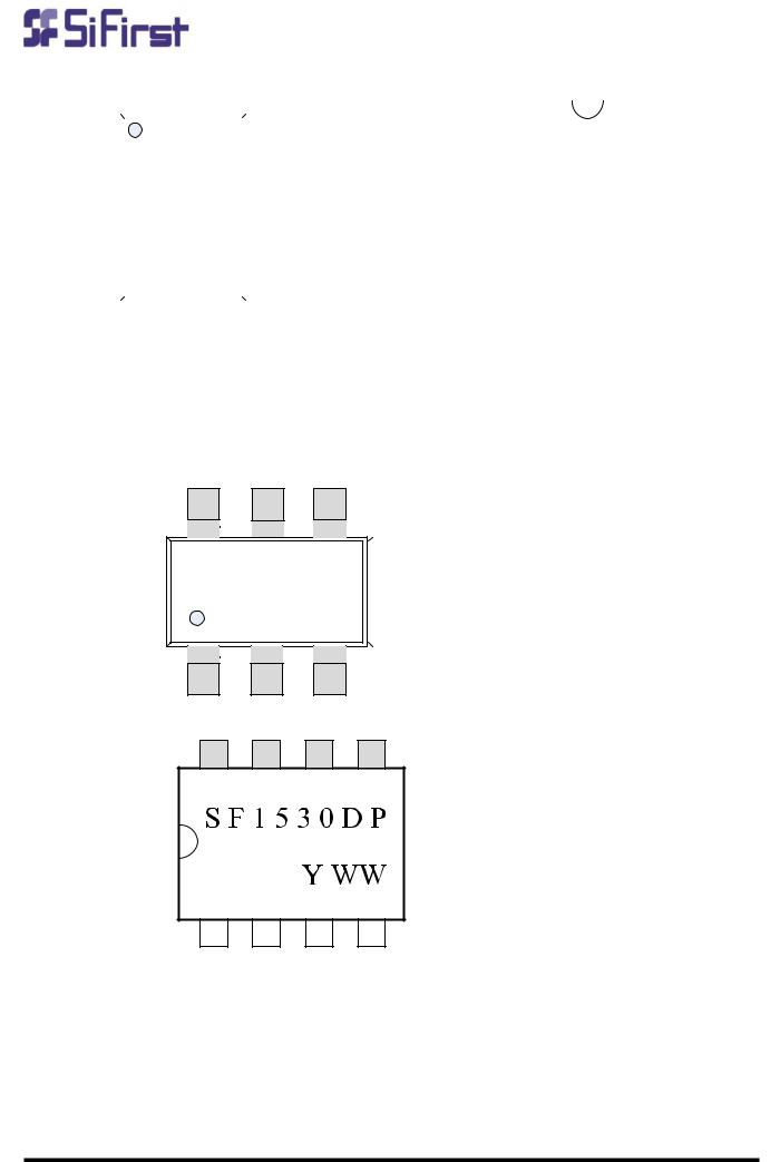
Pin Configuration |
|
|
|
|
|
|
|
|
|
|
|
|
|
|
|
|
|
|||||||
|
|
|
|
|
|
|
|
|
|
|
|
|
|
|
|
|
|
|
1 |
8 |
|
|
GND |
|
|
|
GND |
|
|
|
|
|
1 |
|
6 |
|
|
|
|
GATE |
GATE |
|
|
|
|
||||||
|
|
|
|
|
|
|
|
|
|
|
|
||||||||||||||
|
|
|
|
|
|
|
|
|
|
|
|
|
|
|
DIP8 |
|
|
FB |
|
||||||
|
|
|
|
|
|
|
SOT23-6 |
|
|
|
|
|
|
VDD |
|
2 |
|
|
|
||||||
|
|
|
|
|
|
|
|
|
|
|
|
|
|
7 |
|
|
|
||||||||
|
FB |
|
|
|
|
|
2 |
|
5 |
|
|
|
|
VDD |
|
|
|
|
|
|
|
|
|
|
|
|
|
|
|
|
|
|
3 |
|
4 |
|
|
|
|
CS |
NC |
|
3 |
6 |
|
|
NC |
|
|||
|
|
|
|
|
|
|
|
|
|
|
|
|
|||||||||||||
|
RT |
|
|
|
|
|
|
|
|
|
|
CS |
|
4 |
5 |
|
|
RT |
|
||||||
|
|
|
|
|
|
|
|
|
|
|
|
|
|
|
|||||||||||
|
|
|
|
|
|
|
|
|
|
|
|
|
|
||||||||||||
|
|
|
|
|
|
|
|
|
|
|
|
|
|
|
|
|
|
|
|
||||||
|
|
|
|
|
|
|
|
|
|
|
|
|
|
|
|
|
|
|
|
|
|
|
|
|
|
|
|
|
|
|
|
|
|
|
|
|
|
|
|
|
|
|
|
|
|
|
|
|
|
||
|
Ordering Information |
|
|
|
|
|
|
|
|
|
|
|
|
|
|
|
|
|
|||||||
|
|
|
|
|
|
|
|
|
|
|
|
|
|
|
|
|
|
||||||||
|
Part Number |
|
Top Mark |
|
|
Package |
|
|
|
Tape & Reel |
|
||||||||||||||
|
SF1530LGT |
|
|
.30YWW |
|
|
SOT26 |
|
Green |
|
|
|
Yes |
|
|||||||||||
|
SF1530DP |
|
|
SF1530DP |
|
|
DIP8 |
|
|
RoHS |
|
|
|
|
|
|
|||||||||
Marking Information
YWW: Year&Week code
|
|
|
|
|
|
|
|
|
©SiFirst Technology |
|
|
|
|
|
www.sifirsttech.com |
||
|
- 2 - |
|||||||
SF1530_DS_V1.0

|
|
|
|
|
SF1530 |
Block Diagram |
|
|
|
|
|
|
Oscillator with |
S |
|
|
|
|
Frequency Shuffling |
|
Soft Gate |
GATE |
|
|
|
|
Q |
||
|
|
|
Driver |
|
|
RT |
|
R |
|
|
|
|
|
|
|
||
Zero OCP Recovery |
|
|
|
|
|
Gap Control |
|
Frequency |
|
||
|
|
|
|
||
|
|
Reduction Control |
|
||
RT short/floating |
|
|
|
|
|
protection |
|
|
|
CS floating |
|
|
|
|
|
|
|
|
|
|
|
protection |
|
Trimmed Voltage & |
|
|
|
|
LEB |
Current Reference |
Internal |
|
|
|
CS |
|
blocks |
|
|
|
|
|
|
OCP |
|
Soft start |
|
VDD |
POR |
|
|
|
|
|
|
|
|
||
9V/14V |
|
|
|
|
5.3V |
|
|
|
Slope |
|
|
|
|
|
|
|
|
|
|
|
compensation |
|
|
|
|
|
|
|
FB |
 VDD OVP
Burst Mode
Control
 27.5V
27.5V
33V
GND |
OLP |
43ms Delay |
3.7V
Pin Description
Pin Num |
Pin Name |
I/O |
Description |
1 |
GND |
P |
Ground |
2 |
FB |
I |
Voltage feedback pin. The loop regulation is achieved by connecting a |
|
|
|
photo-coupler to this pin. PWM duty cycle is determined by this pin voltage |
|
|
|
and the current sense signal at Pin 3. |
3 |
RT |
I |
Set the switching frequency by connecting a resistor between RT and |
|
|
|
GND. This pin has floating/short-to-GND protection. |
4 |
CS |
I |
Current sense input pin. |
5 |
VDD |
P |
IC power supply pin. |
6 |
GATE |
O |
Totem-pole gate driver output to drive the external MOSFET. |
Absolute Maximum Ratings (Note 1)
Parameter |
Value |
Unit |
VDD DC Supply Voltage |
33 |
V |
VCC DC Clamp Current |
10 |
mA |
GATE pin |
20 |
V |
FB, RT, CS voltage range |
-0.3 to 7 |
V |
Package Thermal Resistance (SOT-26) |
250 |
oC/W |
Package Thermal Resistance (DIP-8) |
90 |
oC/W |
Package Thermal Resistance (SOP-8) |
150 |
oC/W |
Maximum Junction Temperature |
150 |
oC |
Operating Temperature Range |
-40 to 85 |
oC |
©SiFirst Technology |
www.sifirsttech.com |
|
- 3 - |
SF1530_DS_V1.0

|
|
|
|
|
|
|
|
|
SF1530 |
|
|
|
|
|
|
|
|
|
|
|
|
|
|
|
|
|
|
|
|
|
|
|
|
|
|
|
Storage Temperature Range |
|
|
-65 to 150 |
|
|
oC |
|
|||
|
Lead Temperature (Soldering, 10sec.) |
|
|
|
260 |
|
|
oC |
|
||
|
ESD Capability, HBM (Human Body Model) |
|
|
|
3 |
|
|
kV |
|
||
|
ESD Capability, MM (Machine Model) |
|
|
|
250 |
|
|
V |
|
||
|
Recommended Operation Conditions (Note 2) |
|
|
|
|
|
|
|
|||
|
|
Parameter |
|
|
|
Value |
|
|
Unit |
|
|
|
Supply Voltage, VDD |
|
|
|
11 to 25 |
|
|
V |
|
||
|
Operating Frequency |
|
|
|
50 to 130 |
|
|
kHz |
|
||
|
Operating Ambient Temperature |
|
|
|
-40 to 85 |
|
|
oC |
|
||
|
ELECTRICAL CHARACTERISTICS |
|
|
|
|
|
|
|
|
|
|
|
(TA = 25OC, RT=100K ohm, VDD=18V, if not otherwise noted) |
|
|
|
|
|
|
|
|||
|
Symbol |
Parameter |
Test Conditions |
|
Min |
|
Typ |
Max |
Unit |
|
|
|
Supply Voltage |
Section (VDD Pin) |
|
|
|
|
|
|
|
|
|
|
UVLO(ON) |
VDD Under Voltage |
|
|
13 |
|
14 |
15 |
V |
|
|
|
|
Lockout Exit (Startup) |
|
|
|
|
|
|
|
|
|
|
UVLO(OFF) |
VDD Under Voltage |
|
|
8 |
|
9 |
10 |
V |
|
|
|
|
Lockout Enter |
|
|
|
|
|
|
|
|
|
|
I_Startup |
VDD Start up Current |
VDD =12.5V, Measure |
|
|
|
5 |
20 |
uA |
|
|
|
|
|
current into VDD |
|
|
|
|
|
|
|
|
|
I_VDD_Op |
Operation Current |
VFB=3V,CL=1nF |
|
|
|
2.5 |
3.5 |
mA |
|
|
|
VDD_OVP |
VDD Over Voltage |
|
|
25 |
|
27.5 |
30 |
V |
|
|
|
|
Protection trigger |
|
|
|
|
|
|
|
|
|
|
VDD_Clamp |
VDD Zener Clamp |
I(VDD ) = 15 mA |
|
|
|
33 |
|
|
V |
|
|
|
Voltage |
|
|
|
|
|
|
|
|
|
|
T_Softstart |
Soft Start Time |
|
|
|
|
3 |
|
|
mSec |
|
|
Feedback Input |
Section(FB Pin) |
|
|
|
|
|
|
|
|
|
|
VFB_Open |
FB Open Voltage |
|
|
|
|
5.3 |
|
|
V |
|
|
|
|
|
|
|
|
|
|
|
|
|
|
IFB_Short |
FB short circuit |
Short FB pin to GND, |
|
|
|
1.1 |
|
|
mA |
|
|
|
current |
measure current |
|
|
|
|
|
|
|
|
|
AVCS |
PWM Input Gain |
VFB / Vcs |
|
|
|
2.0 |
|
|
V/V |
|
|
VFB_min_duty |
FB under voltage gate |
|
|
|
|
1.0 |
|
|
V |
|
|
|
clock is off. |
|
|
|
|
|
|
|
|
|
|
VTH_PL |
Power Limiting FB |
|
|
|
|
3.7 |
|
|
V |
|
|
|
Threshold Voltage |
|
|
|
|
|
|
|
|
|
|
TD_PL |
Power limiting |
Note 3 |
|
|
|
43 |
|
|
mSec |
|
|
|
Debounce Time |
|
|
|
|
|
|
|
|
|
|
ZFB_IN |
Input Impedance |
|
|
|
|
5 |
|
|
Kohm |
|
|
Current Sense |
Input Section (CS Pin) |
|
|
|
|
|
|
|
|
|
|
Vth_OC_min |
Internal current |
Zero duty cycle |
|
0.70 |
|
0.75 |
0.80 |
V |
|
|
|
|
limiting threshold |
|
|
|
|
|
|
|
|
|
|
T_blanking |
SENSE Input Leading |
|
|
|
|
250 |
|
|
nSec |
|
|
|
Edge Blanking Time |
|
|
|
|
|
|
|
|
|
|
TD_OC |
Over Current |
CL=1nF at GATE, |
|
|
|
70 |
|
|
nSec |
|
|
|
Detection and Control |
|
|
|
|
|
|
|
|
|
|
|
Delay |
|
|
|
|
|
|
|
|
|
|
Oscillator Section |
(RT Pin) |
|
|
|
|
|
|
|
|
|
|
FOSC |
Normal Oscillation |
|
|
60 |
|
65 |
70 |
KHZ |
|
|
|
|
Frequency |
|
|
|
|
|
|
|
|
|
|
RT_range |
Operating RT Range |
|
|
50 |
|
100 |
150 |
Kohm |
|
|
|
V_RT_open |
RT open voltage |
|
|
|
|
2.0 |
|
|
V |
|
|
∆F(shuffle)/Fosc |
Frequency shuffling |
Note 4 |
|
-4 |
|
|
4 |
|
% |
|
|
|
range |
|
|
|
|
|
|
|
|
|
|
∆f_Temp |
Frequency |
-20oC to 100 oC (Note 4) |
|
|
|
5 |
|
|
% |
|
|
|
Temperature Stability |
|
|
|
|
|
|
|
|
|
|
∆f_VDD |
Frequency Voltage |
VDD = 12-25V, |
|
|
|
5 |
|
|
% |
|
|
|
|
|
|
|
|
|
|
|
|
|
©SiFirst Technology |
www.sifirsttech.com |
|
- 4 - |
SF1530_DS_V1.0
 Loading...