

Page 1
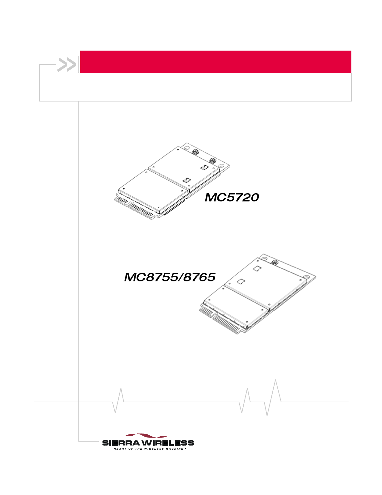
MC5720, MC8755, MC8765 MiniCard
Hardware Integration Guide
Proprietary and Confidential
2130114
Rev 0.92
Page 2

Page 3
Preface
Limitation of
Liability
Patents
The information in this manual is subject to change without
notice and does not
Wireless. SIERRA WIRELESS AND ITS AFFILIATES
Sierra
SPECIFICALLY DISCLAIM LIABILITY FOR ANY AND ALL
DIRECT, INDIRECT, SPECIAL, GENERAL, INCIDENTAL,
CONSEQUENTIAL, PUNITIVE OR EXEMPLARY DAMAGES
INCLUDING, BUT NOT LIMITED TO, LOSS OF
REVENUE OR ANTICIPATED PROFITS OR REVENUE
ARISING OUT OF THE
SIERRA
AND/OR ITS
POSSIBILITY OF
FORESEEABLE OR FOR CLAIMS BY ANY THIRD PARTY.
Notwithstanding the foregoing, in no event shall Sierra
Wireless and/or its affiliates aggregate liability arising under or
in connection with the Sierra
the
liability, be in excess of the price paid by the purchaser for the
Sierra
Portions of this product may be covered by some or all of the
following US patents:
5,515,013 5,629,960 5,845,216 5,847,553 5,878,234
5,890,057 5,929,815
6,339,405 6,359,591
6,561,851 6,653,979
6,847,830 6,876,697
D459,303
and other patents pending.
WIRELESS PRODUCT, EVEN IF SIERRA WIRELESS
number of events, occurrences, or claims giving rise to
Wireless
represent a commitment on the part of
PROFITS OR
USE OR INABILITY TO USE ANY
AFFILIATES HAS BEEN ADVISED OF THE
SUCH DAMAGES OR THEY ARE
Wireless product, regardless of
product.
6,169,884 6,191,741 6,199,168
6,400,336 6,643,501 6,516,204
6,697,030 6,785,830 6,845,249
6,879,585 6,886,049 D442,170
This product
technology
Licensed by QUALCOMM Incorporated under one or more of
following United States patents and/or their counterparts
the
other nations:
in
4,901,307 5,056,109 5,101,501 5,109,390 5,228,054
5,267,261 5,267,262
5,490,165 5,504,773
5,544,196 5,568,483
5,710,784 5,778,338
Manufactured or sold by Sierra Wireless or its licensees under
one or more patents
Copyright
Rev 0.92 Nov.05 1
©2005 Sierra Wireless. All rights reserved.
includes
licensed from:
5,337,338 5,414,796 5,416,797
5,506,865 5,511,073 5,535,239
5,600,754 5,657,420 5,659,569
licensed from InterDigital Group.
Page 4
MC5720/8755/8765 Hardware Integration Guide
Trademarks
Contact
Information
AirCard and “Heart of the Wireless Machine” are registered
trademarks of Sierra Wireless.
Wireless, the Sierra Wireless logo, the red wave design,
Sierra
red‐tipped antenna, and Wat cher are trademarks of Sierra
the
Wireless.
Windows
Qualcomm
®
is a registered trademark of Microsoft Corporation.
®
is a registered trademark of Qualcomm Incorpo‐
rated.
Other trademarks are the property of the respective owners.
Sales Desk: Phone: 1-604-232-1488
Hours: 8:00 AM to 5:00 PM Pacific Time
E-mail: sales@sierrawireless.com
Post: Sierra Wireless
13811 Wireless Way
Richmond, BC
Canada V6V 3A4
Fax: 1-604-231-1109
Web: www.sierrawireless.com
Consult our website for up‐to‐date product descriptions,
documentation, application notes, firmware upgrades, trouble‐
shooting tips, and press releases:
www.sierrawireless.com
2 2130114
Page 5

Table of Contents
Introduction . . . . . . . . . . . . . . . . . . . . . . . . . . . . . . . . . . . . . . . . . . . . . . .5
The Universal Development Kit . . . . . . . . . . . . . . . . . . . . . . . . . . . . . . . . . . . . . . 5
Required connectors . . . . . . . . . . . . . . . . . . . . . . . . . . . . . . . . . . . . . . . . . . . . . . . 5
Guide Organization . . . . . . . . . . . . . . . . . . . . . . . . . . . . . . . . . . . . . . . . . . . . . . . . . 6
Related documents. . . . . . . . . . . . . . . . . . . . . . . . . . . . . . . . . . . . . . . . . . . . . . . . . 6
Power Interface . . . . . . . . . . . . . . . . . . . . . . . . . . . . . . . . . . . . . . . . . . . .9
Overview of operation. . . . . . . . . . . . . . . . . . . . . . . . . . . . . . . . . . . . . . . . . . . . . . . 9
Power signals . . . . . . . . . . . . . . . . . . . . . . . . . . . . . . . . . . . . . . . . . . . . . . . . . . 9
Electrostatic discharge (ESD) . . . . . . . . . . . . . . . . . . . . . . . . . . . . . . . . . . . . 9
Module power states . . . . . . . . . . . . . . . . . . . . . . . . . . . . . . . . . . . . . . . . . . . . . . 10
Disconnected state . . . . . . . . . . . . . . . . . . . . . . . . . . . . . . . . . . . . . . . . . . . . 10
Off state . . . . . . . . . . . . . . . . . . . . . . . . . . . . . . . . . . . . . . . . . . . . . . . . . . . . . . 10
Normal state . . . . . . . . . . . . . . . . . . . . . . . . . . . . . . . . . . . . . . . . . . . . . . . . . . 11
Low power mode . . . . . . . . . . . . . . . . . . . . . . . . . . . . . . . . . . . . . . . . . . . . . . 11
Usage models . . . . . . . . . . . . . . . . . . . . . . . . . . . . . . . . . . . . . . . . . . . . . . . . . 11
RF Integration . . . . . . . . . . . . . . . . . . . . . . . . . . . . . . . . . . . . . . . . . . . .13
RF connection . . . . . . . . . . . . . . . . . . . . . . . . . . . . . . . . . . . . . . . . . . . . . . . . . . . . 13
Ground connection . . . . . . . . . . . . . . . . . . . . . . . . . . . . . . . . . . . . . . . . . . . . . . . . 13
Shielding . . . . . . . . . . . . . . . . . . . . . . . . . . . . . . . . . . . . . . . . . . . . . . . . . . . . . 14
Antenna and cabling . . . . . . . . . . . . . . . . . . . . . . . . . . . . . . . . . . . . . . . . . . . 14
Interference and sensitivity . . . . . . . . . . . . . . . . . . . . . . . . . . . . . . . . . . . . . . . . . 15
Power supply noise . . . . . . . . . . . . . . . . . . . . . . . . . . . . . . . . . . . . . . . . . . . . 15
Interference from other wireless devices . . . . . . . . . . . . . . . . . . . . . . . . . . 15
Device-generated RF . . . . . . . . . . . . . . . . . . . . . . . . . . . . . . . . . . . . . . . . . . . 16
Host/Module Communication Interface . . . . . . . . . . . . . . . . . . . . .17
Rev 0.92 Nov.05 3
Page 6

MC5720/8755/8765 Hardware Integration Guide
LED output . . . . . . . . . . . . . . . . . . . . . . . . . . . . . . . . . . . . . . . . . . . . . . . . . . . 17
Regulatory Information . . . . . . . . . . . . . . . . . . . . . . . . . . . . . . . . . . . 19
Important notice . . . . . . . . . . . . . . . . . . . . . . . . . . . . . . . . . . . . . . . . . . . . . . . . . . 19
Safety and hazards . . . . . . . . . . . . . . . . . . . . . . . . . . . . . . . . . . . . . . . . . . . . . . . . 19
Important compliance information for North American users . . . . . . . . . . . 20
Acronyms and Definitions . . . . . . . . . . . . . . . . . . . . . . . . . . . . . . . . . 23
Index 25
4 2130114
Page 7
1: Introduction
Sierra Wireless’ MiniCard modules form the radio component
the products in which they are embedded. MiniCards are
for
available for use on CDMA and GSM networks, including:
• MC5720 — operates on CDMA networks using the IS‐95A
and CDMA 1X, and
• MC8755 and MC8765 — operates on GSM networks using
the
Purpose of this guide
This guide addresses issues that affect the integration of Sierra
Wireless modules into host products, and includes design
recommendations for the host products.
Note: An understanding of network technology and experience in
integrating hardware components into electronic equipment is
assumed.
The Universal Development Kit
1
1xEV‐DO (IS‐866) network standards
GSM/GPRS/EDGE/UMTS/HSDPA network standards
Note: Contact vendors before
choosing your connectors — the
numbers included here are for
reference only. Choose
connectors that are appropriate
to your design.
Sierra Wireless manufactures a Universal Development Kit
(UDK)
This kit is a hardware development platform that is designed
to
Module product family. It contains the hardware components
that are typically necessary for evaluating and developing with
the module,
• Development board
• Cables
• Antennas
• Other accessories
that facilitates all phases of the integration process.
support multiple members of the Wireless Embedded
including:
Required connectors
When integrating these modules into your host device, you
need the
• RF cable that mates with Hirose U.FL connector (model
• Industry‐standard mating connector for 52‐pin EDGE:
following connector types:
U.FL #CL331‐0471‐0‐10)
Some manufacturers
example, the
connector used on the MC5720/MC8755/
include Tyco, Foxconn, and Molex. For
Rev 0.92 Nov.05 5
Page 8

MC5720/8755/8765 Hardware Integration Guide
MC8765 Universal Development Kit board is a Molex
67910‐0001.
• Industry‐standard USIM/RUIM connector: The actual
connector
USIM/RUIM socket. For example, the USIM/RUIM
connector used on the
Development Kit is an ITT CCM03‐3518.
Guide Organization
This guide includes the following sections:
1. Introduction (this section)
2. Power Interface (p.9)
Describes power control signals used by the module and
discusses design issues related to power supply
integration.
3. RF Integration (p.13)
Describes antenna connection methods and grounding issues,
RF
4. Host/Module Communication Interface (p.17)
Describes the USB interface for host/module communication,
and the USIM/RUIM interface for host/module integration.
5. Acronyms and Definitions (p.23)
Lists
6. Regulatory Information (p.19)
Describes regulatory approvals and regulatory information
requirements.
you use depends on how your device exposes the
MC5720/MC8755/MC8765 Universal
interference and desense issues.
acronyms and definitions used throughout this guide.
Note: The term "host" always refers to the host device.
Related documents
This guide deals specifically with hardware integration issues
that are unique to the MC5720 and MC8755/8765 modules.
Tabl e 1‐1 lists other documents referenced in this guide.
6 2130114
Page 9
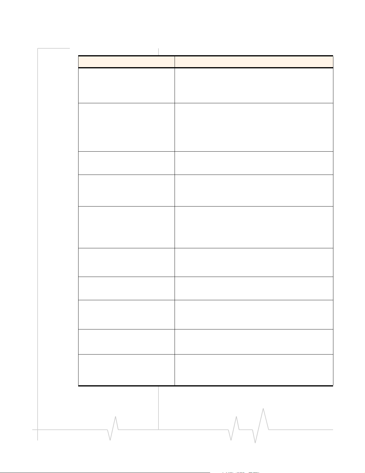
Table 1-1: Related documentation
Document title Description
Introduction
AT Command Set for User
Equipment (UE) (Release 6)
CDMA 1X Standard
EM5625/MC5720 CnS
Reference (Document
2130643)
EMXXXX Embedded Modem
Extended AT Command
Reference (Document
2130395)
FCC Regulations - Part 15 -
Radio Frequency Devices
This 3GPP technical specification describes standard AT
commands for GSM/UMTS devices.
The document (3GPP TS 27.007) can be downloaded
from www.3gpp.org.
This standard describes the technical requirements for
CDMA systems, including details on sleep cycle index
(SCI) values.
The document, CDMA 2000 Series Release A (2000)
(document # TIA/EIA/IS-2000 Series, Release A) can be
ordered from www.tiaonline.org.
This document describes the CnS (Control and Status)
messages that are available for use with the MC5720.
This document describes proprietary AT commands for the
MC5720. For MC8755/MC8765-specific commands, see
MC87xx Modem Extended AT Command Reference
(Document 2130616)
This section of the FCC Code of Federal Regulations, T itle
47 deals with radio frequency devices, including EM
shielding requirements.
The regulation can be downloaded from
http://wireless.fcc.gov.
IEC-61000-4-2 level 3
MC5720 MiniCard Product
Specification (Document
2130599)
MC8755/MC8765 PCI Express
MiniCard Product
Specification (Document
2130637)
MC87xx Modem CnS Reference
(Document 2130602)
MC87xx Modem Extended AT
Command Reference
(Document 2130616)
This document describes techniques for testing and
measuring electrostatic discharge (ESD) immunity.
The document can be ordered from www.iec.ch.
This document describes the mechanical and electrical
specifications, and standards compliance of the MC5720.
This document describes the mechanical and electrical
specifications, and standards compliance of the MC8755/
MC8765.
This document describes the CnS (Control and Status)
messages that are available for use with the MC8755/
MC8765.
This document describes proprietary AT commands for the
MC8755/MC8765. For MC5720-specific commands, see
the EMXXXX Embedded Modem Extended AT Command
Reference (Document 2130395)
Rev 0.92 Nov.05 7
Page 10
MC5720/8755/8765 Hardware Integration Guide
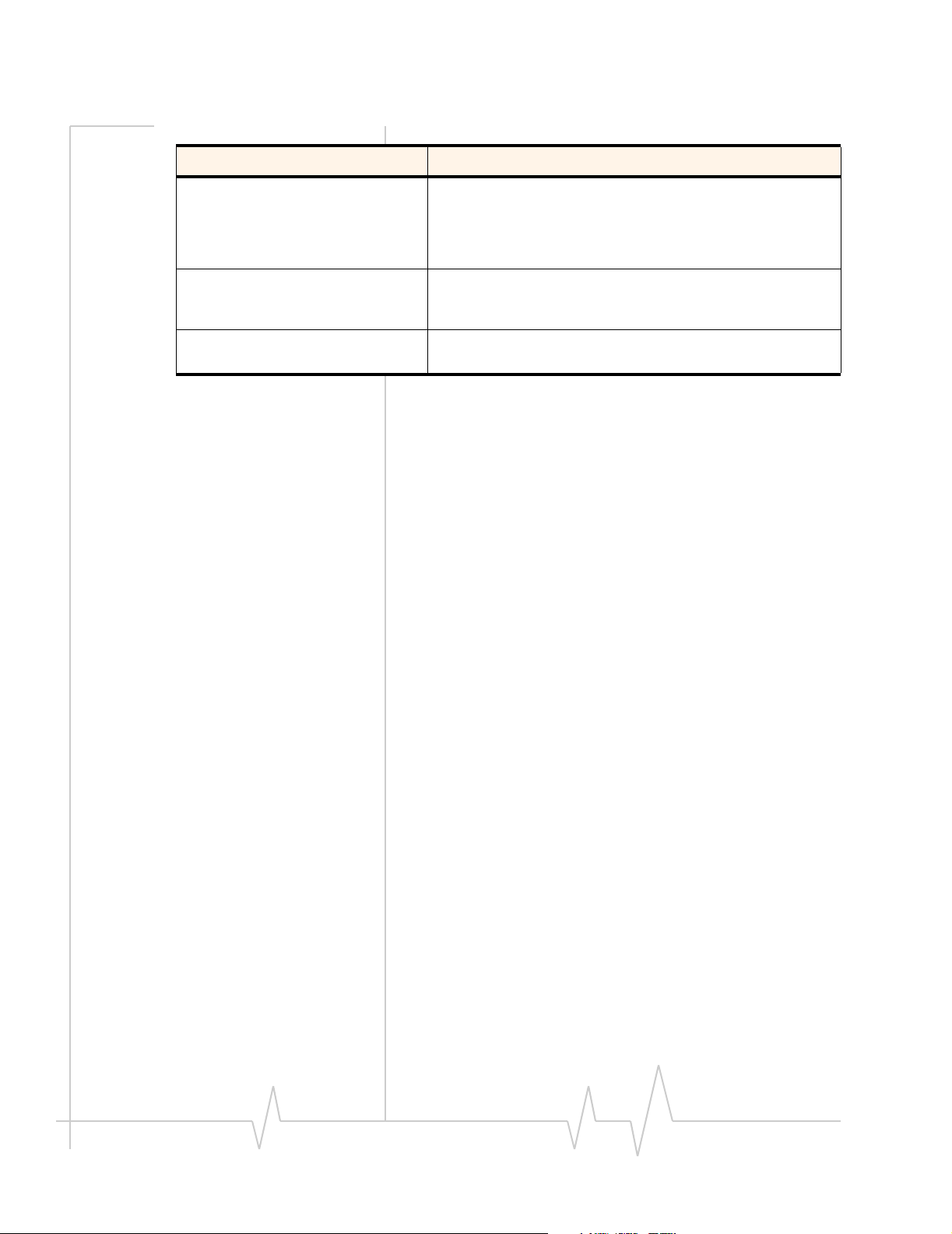
Table 1-1: Related documentation
Document title Description
Mobile Station (MS)
Conformance Specification;
Part 4: Subscriber Interface
Module
PCI Express Mini Card
Electromechanical
Specification Revision 1.1
Universal Serial Bus
Specification, Rev 2.0
This 3GPP technical specification describes SIM testing
methods.
The document (3GPP TS 11.10-4) can be downloaded
from www.3gpp.org.
The document can be downloaded from www.pcisig.com.
The specification can be downloaded from www.usb.org.
8 2130114
Page 11

2: Power Interface
Overview of operation
Note: This chapter contains information for both the CDMA (MC5720)
and GSM (MC8755/8765) modules.
Information that is unique to one module type is clearly identified.
The module is designed to use a 3.3V (nominal) power supply,
provided by the host. It is the
safe and continuous
module
protection circuits to guard against electrical issues.
The module’s power state is controlled by the host’s assertion/
de‐assertion of the
monitors
supply is insufficient.
Power signals
does NOT have an independent power supply, or
its supply voltage and requests shutdown if the
2
host’s responsibility to provide
power to the module at all times; the
W_Disable# signal. The module also
The module must be connected to a 3.3V power supply (as
indicated in PCI Express Mini Card Electromechanical Specifi‐
cation Revision 1.1).
The MC8755/8765 has more power pins than the MC5720 due
to higher
For detailed pinout and voltage / current requirements of these
modules,
(Document
MiniCard Product Specification (Document 2130637).
peak current requirements for GSM devices.
refer to MC5720 MiniCard Product Specification
2130599) and MC8755/MC8765 PCI Express
Electrostatic discharge (ESD)
You are responsible for ensuring that the host has adequate
ESD protection on
• (Operational) RF port (antenna launch and RF connector):
IEC‐61000‐4‐2 — Level (Electrostatic Discharge Immunity Test)
• (Non‐operational) Host connector interface:
JESD22‐A114‐B+/‐ 1kV Human Body Model and
JESD22‐C101 +/‐ 125 V Charged Device Model
Specific recommendations are provided where needed in this
guide, however, the level of protection required depends on
your application.
digital circuits and antenna ports:
Rev 0.92 Nov.05 9
Page 12

MC5720/8755/8765 Hardware Integration Guide
Note: ESD protection is highly recommended for the SIM connector
at the point where the contacts are exposed, and any other signals
from the host interface that would be subjected to ESD by the user of
the end product.
Module power states
Note: The modul e un i t defaults
to the Normal state when
VCC3.3 is first applied in the
absence of W_Disable# control.
Note: The differ en ce b e t w ee n
the Disconnected and Off states
is that in the Off state, the
module is still connected to the
power source and draws minimal
current.
At any time, the module will be in one of four power states:
• Disconnected
No power to the module.
• Off
Power to the module, but the module is powered off.
• Normal
The module is active. Several modes are possible (Receive,
Tra nsmit, Sleep, Shutdown).
• Low power (“airplane mode”)
The module is active, but RF is disabled.
State machines are implemented in the module to monitor the
power supply and operating temperature.
Disconnected state
This state occurs when there is no power to the module — the
power source is disconnected from the module and all
host
voltages associated with the module are at 0V.
Whether the host device is also powered off depends on the
power rail design. If the connection between the power rail
and the module is
powered on and cut the power to put the modem into the
disconnected
device and the module, the host is powered off when the
module is
powered off.
controlled by the host, the host can stay
state. If the power rail is
shared between the host
Off state
In this state, the host is powered up and the module is
powered down (but still connected to the power source).
The host keeps the module powered off by asserting (driving
low) the
minimal current.
10 2130114
W_Disable# signal. In this state, the module draws
Page 13
Normal state
Power Interface
Note: This is the default state
when VCC3.3 is first applied in
the absence of W_Disable#
control.
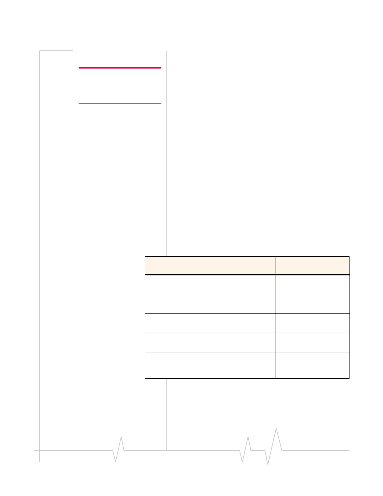
Table 2-1: Power consumption of a sample application
This is the active state of the module. While in this state:
• The module is fully powered.
• The module is capable of placing/receiving calls or estab‐
lishing data connections on the wireless network.
• The USB interface is fully active.
Low power mode
In this power state, RF (both Rx and Tx) is disabled in the
module, but the
(ʺairplane modeʺ) is controlled by a software command
mode
through the host interface.
instructions on using appropriate commands, refer to AT
For
Command Set for User Equipment (UE) (Release 6) (+CFUN=0
command), EM5625/MC5720 CnS Reference (Document 2130643)
(CNS_RADIO_POWER [0x1075]), or MC87xx Modem CnS
Reference (Document 2130602) (Disable Modem).
USB interface is still active. This low power
Usage models
Usage models can be used to calculate expected current
consumption. A
sample usage model is provided in Tabl e 2‐1.
Upload
(module Tx)
Download
(module Rx)
Coverage /
data rate
Hours of
operation
Total power
consumed
over 24 hours
This example model
practice, because the module
(the host device manages the power source), the mAh ratings
will depend on the device’s supply efficiency.
Used by a field worker
(data only)
1000 kB/day 40 kB/h
500 kB/day 100 kB/day
1X / 80 kbps IS-95 / 14.4 kbps
8 / day (off 16 hrs / day) 24 / day
60 mAh 200 mAh
applies to a battery‐operated device. In
will be isolated from the battery
Used for remote data
logging
Rev 0.92 Nov.05 11
Page 14

MC5720/8755/8765 Hardware Integration Guide
The module automatically enters slotted sleep mode when
there is no transmission or reception occurring (SCI = 2).
Tra nsmit power is assumed to be +3 dBm .
12 2130114
Page 15

3: RF Integration
RF connection
Consider the following when attaching an antenna to the
module:
3
Note: To disconnect the
antenna, make sure you use the
Hirose U.FL connector removal
tool (P/N UFL-LP-N-2(01) to
prevent damage to the module
or coaxial cable assembly.
• Use a Hirose U.FL connector (model
U.FL #CL331‐0471‐0‐10) to attach an antenna to a
connection point on the module, as shown in Figure 3‐1
(The main RF connector on the top side; the diversity RF
connector on the bottom
• Match coaxial connections between the module and the
antenna to 50 Ω.
• Minimize RF cable losses to the antenna; the recommended
maximum cable
Figure 3-1: Antenna connection points and mounting holes
loss for antenna cabling is 0.5 dB.
side).
Ground connection
When connecting the module to system ground:
• Prevent noise leakage by establishing a very good ground
connection to the module through the host
• Connect to system ground using the two mounting holes at
the top of the module (as shown in Figure 3‐1).
• Minimize ground noise leakage into the RF.
Depending on the host board design, noise could potentially
be coupled to the module from the
mainly an
along the
both ends of
Rev 0.92 Nov.05 13
issue for host designs that have signals traveling
length of the module, or circuitry operating at
the module
interconnects.
host board. This is
connector.
Page 16

MC5720/8755/8765 Hardware Integration Guide
Shielding
The module is fully shielded to protect against EMI and to
ensure
Devices” (or equivalent regulations in other jurisdictions).
Note: The module shields must NOT be removed.
Antenna and cabling
When selecting the antenna and cable, it is critical to RF perfor‐
mance to match antenna gain and cable loss.
Choosing the correct antenna and cabling
Consider the following points for proper matching of antennas
and cabling:
• The antenna (and associated circuitry) should have a
nominal
across each frequency band of operation.
• The system gain value affects both radiated power and
regulatory (FCC, IC, CE, etc.)
compliance with FCC Part 15‐ “Radio Frequency
impedance of 50 Ω with a return loss ≤ 10 dB
test results.
Developing custom antennas
Consider the following points when developing custom‐
designed antennas:
• A skilled RF engineer should do the development to ensure
that the RF performance is maintained.
• Identify the bands that need to be supported, particularly
when both the
in the same
separate
Determining the antenna’s location
Consider the following points when deciding where to put the
antenna:
• Antenna location may affect RF performance. Although the
module is
tions, the placement of the antenna is still very important‐
if the host
broadband or
performance.
• Connecting cables between the module and the antenna
have 50 Ω impedance. If the impedance of the module
must
mismatched, RF performance is reduced significantly.
is
• Antenna cables should be routed, if possible, away from
sources (switching power supplies, LCD assemblies,
noise
MC5720 and MC8755/8765 will be installed
platform. In this case, you may want to develop
antennas for maximum performance.
shielded to prevent interference in most applica‐
device is insufficiently shielded, high levels of
spurious noise can degrade the module’s
14 2130114
Page 17

RF Integration
etc.). If the cables are near the noise sources, the noise may
be coupled into the RF cable and into the antenna.
Disabling the diversity antenna (MC5720)
If your host device is not designed to use the MC5720’s
diversity antenna, terminate the interface with a no‐connect.
Interference and sensitivity
Note: These modules are based
on ZIF (Zero Intermediate
Frequency) technologies; when
performing EMC
(Electromagnetic Compatibility)
tests, there are no IF
(Intermediate Frequency)
components from the module to
consider.
Several sources of interference can affect the RF performance
of the module (RF
supply noise and device‐generated RF.
RF desense can be addressed through a combination of
mitigation techniques and radiated sensitivity measurement.
desense). Common sources include power
Power supply noise
Noise in the power supply can lead to noise in the RF signal.
The power supply ripple limit for the module is no more than
200 mVp‐p1Hz to 100 kHz. This limit includes voltage ripple
due to
transmitter burst activity
Interference from other wireless devices
Different wireless devices operating inside the host device can
interference that affects the module.
cause
To determine the most suitable locations for each antenna on
your host device, evaluate each wireless device’s radio system,
considering the following:
• Any harmonics, sub‐harmonics, or cross‐products of signals
generated by wireless devices that fall in the module’s Rx
may cause spurious response resulting in decreased
range
Rx performance.
• The Tx power and corresponding broadband noise of other
wireless devices may overload or increase the noise floor of
module’s receiver, resulting in Rx desense.
the
The severity of this interference depends on the closeness of
the other antennas to
suitable locations for each wireless device’s antenna,
thoroughly evaluate your host device’s design.
Rev 0.92 Nov.05 15
the module’s antenna. To determine
Page 18

MC5720/8755/8765 Hardware Integration Guide
Device-generated RF
Note: The module can cause
interference with other devices
such as hearing aids and onboard speakers.
Wireless devices such as the
MiniCard transmit in bursts
(pulse transients), for set
durations (RF burst frequencies).
Hearing aids and speakers
convert these burst frequencies
into audible frequencies,
resulting in audible noise.
All electronic computing devices generate RF interference that
negatively affect the receive sensitivity of the module
can
desense).
(RF
The proximity of host electronics to the antenna in wireless
devices can contribute to RF desense. Components that are
likely to cause RF desense include:
most
• Microprocessor and memory
• Display panel and display drivers
• Switching‐mode power supplies
These, and other high‐speed devices (in particular, the
processor) can cause RF desense because they run at
frequencies of tens of MHz. The rapid rise and fall of these
clock signals generates
higher‐order harmonics that often fall
within the operating frequency band of the module, causing
desense.
RF
Example
On a sub‐system running at 40 MHz, the 22nd harmonic falls
MHz, which is within the cellular receive frequency
at 880
band.
Note: In practice, there are usually numerous interfering frequencies
and harmonics. The net effect can be a series of desensitized receive
channels.
16 2130114
Page 19

4: Host/Module Communication Interface
This chapter provides information about the Host‐Module
communication
commands that may be useful for hardware integration
AT
testing.
Note: On any given interface (USB, USIM/RUIM, etc.), leave unused
inputs and outputs as no-connects.
LED output
The module drives the LED output according to the PCI‐
Express MiniCard specification (summarized in Table 4 ‐1,
below).
Table 4-1: LED States
State Indicates Characteristics
interface (USB interface) and lists of extended
4
OFF
ON
Slow Blink
Intermittent
Blink
Module is not
powered.
Module is powered
and connected, but
not transmitting or
receiving.
Module is powered
and searching for a
connection.
Module is transmitting LED is flashing intermittently,
or receiving. proportional to activity on the
Light is turned off.
Light is turned on.
LED is flashing at a steady,
slow rate.
• 250 ms ± 25% ON period
• 0.2 Hz ± 25% blink rate
interface.
• 50% duty cycle
• 3 Hz minimum blink rate
• 20 Hz maximum blink rate
Rev 0.92 Nov.05 17
Page 20

MC5720/8755/8765 Hardware Integration Guide
Figure 4-1: Example LED
MiniCard
MIO
VCC 3.3V
Current limiting Resistor
LED
18 2130114
Page 21

5: Regulatory Information
Important notice
Because of the nature of wireless communications, trans‐
mission and reception of data can never be guaranteed. Data
may be
Although
wireless devices such as the Sierra Wireless modem are used in
a normal
Wireless modem should not be used in situations where failure
to
to the user or any other
personal
its affiliates accept no responsibility for damages of any kind
resulting from delays or errors in data transmitted or received
using the Sierra Wireless modem, or for failure of the Sierra
Wireless modem to transmit or receive such data.
Safety and hazards
delayed, corrupted (i.e., have errors) or be totally lost.
significant delays or losses of data are rare when
manner with a well‐constructed network, the Sierra
transmit or receive data could result in damage of any kind
party, including but not limited to
injury, death, or loss of property. Sierra
5
Wireless and
Do not operate your MC5720/MC8755/MC8765 modem:
• In areas where blasting is in progress
• Where explosive atmospheres may be present including
refuelling points,
• Near medical equipment
• Near life support equipment, or any equipment which may
susceptible to any form of radio interference. In such
be
areas, the MC5720/MC8755/MC8765 modem MUST BE
POWERED
MC8765 modem can transmit signals that could interfere
with this
In an aircraft, the MC5720/MC8755/MC8765 modem MUST BE
POWERED
modem can transmit signals that could interfere with
onboard systems and may be dangerous to the operation of the
aircraft or
in an aircraft is
this instruction may lead to suspension or denial of cellular
telephone services to the offender, or legal action or both.
Some airlines may permit the use of cellular phones while the
aircraft is on the ground and the door is open. The
MC8755/MC8765 modem may be used normally at this time.
equipment.
OFF. Otherwise, the MC5720/MC8755/MC8765
disrupt the cellular network. Use of a cellular phone
fuel depots, and chemical plants
OFF. Otherwise, the MC5720/MC8755/
illegal in some jurisdictions.
Failure to observe
MC5720/
various
Rev 0.92 Nov.05 19
Page 22

MC5720/8755/8765 Hardware Integration Guide
Important compliance information for North American users
The MC5720/MC8755/MC8765 modem has been granted
modular
MC5720/MC8755/MC8765 modem in their final products
the
without additional FCC / IC
they meet the following conditions. Otherwise, additional
FCC / IC
1. At least 20 cm separation distance between the antenna and
the
2. To comply with FCC / IC regulations limiting both maximum
RF output
maximum antenna gain including cable loss in a mobile‐only
exposure
· 8dBi in the Cellular band and 4dBi in the PCS band for the
· 4.65 dBi in the Cellular band and 3.35 dBi in the PCS band
3. The MC5720/MC8755/MC8765 modem and its antenna
must not be
any other
4. A label must be affixed to the outside of the end product into
which the
rated, with a statement similar to the following:
· For MC5720:
· For MC8755:
· For MC8765:
5. A user manual with the end product must clearly indicate the
operating
to ensure
guidelines.
The end product with an embedded MC5720/MC8755/MC8765
modem may
emission testing
Part 15.
FCC
approval for mobile applications. Integrators may use
(Industry Canada) certification if
approvals must be obtained.
user’s body must be maintained at all times.
power and human exposure to RF radiation, the
condition must not exceed:
MC8755/MC8765
for the MC5720
co‐located or operating in conjunction with
transmitter or antenna within a host device.
MC5720/MC8755/MC8765 modem is incorpo‐
This device contains TX FCC ID: N7N‐MC5720
This equipment contains equipment certified under
IC:
2417C‐MC5720
This device contains TX FCC ID: N7NMC8755
This equipment contains equipment certified under
IC:
2417C‐MC8755
This device contains TX FCC ID: N7NMC8765
This equipment contains equipment certified under
2417C‐MC8765
IC:
requirements and conditions that must be observed
compliance with current FCC / IC RF exposure
also need to pass the FCC Part 15 unintentional
requirements and be properly authorized per
20 2130114
Page 23

Regulatory Information
Note: If this module is intended for use in a portable device,
you are responsible for separate approval to satisfy the SAR
requirements of FCC
Part 2.1093 and IC RSS‐102.
Rev 0.92 Nov.05 21
Page 24

MC5720/8755/8765 Hardware Integration Guide
22 2130114
Page 25

A: Acronyms and Definitions
.
Table 5-1: Acronyms and definitions
Acronym or term Definition
AGC Automatic Gain Control
BER Bit Error Rate - a measure of receive sensitivity
BLER Block Error Rate
Call Box Base Station Simu lator - Agilent E8285A or 8960, Rohde &
Schwarz CMU200
CDMA Code Division Multiple Access
dB Decibel = 10 x log10 (P1/P2)
P1 is calculated power; P2 is reference power
Decibel = 20 x log10 (V1/V2)
V1 is calculated voltage, V2 is reference voltage
dBm Decibels, relative to 1 mW - Decibel(mW) = 10 x log10 (Pwr (mW)/
1mW)
A
DUT Device Under Test
EDGE Enhanced Data rates for GSM Evolution
EM Embedded Module
ESD ElectroStatic Discharge
FER Frame Error Rate - a measure of receive sensitivity
GPRS General Packet Radio Service
GPS Global Positioning System
GSM Global System for Mobile communications
Hz Hertz = 1 cycle/second
inrush current Peak current drawn when a device is connected or powered on
IS-2000 3G radio standards for voice and data (CDMA only)
IS-95 2G radio standards targeted for voice (cdmaONE)
LDO Low Drop Out - refers to linear regulator
MC5720 Sierra Wireless MiniCard used on CDMA networks
Rev 0.92 Nov.05 23
Page 26

MC5720/8755/8765 Hardware Integration Guide
Table 5-1: Acronyms and definitions
Acronym or term Definition
MC8755 / MC8765 Sierra Wireless MiniCards used on GSM networks
MHz MegaHertz = 10E6 Hertz (Hertz = 1 cycle/second)
MIO Module Input/Output
MPE Maximum Permissible Exposure — the level of radiation to which a
person may be exposed without hazardou s effect or adve rs e
biological changes
OTA Over The Air or Radiated through the antenna
PCS Personal Communication System - PCS spans the 1.9 GHz radio
spectrum
RF Radio Frequency
RMS Root Mean Square
RUIM Removable User Identity Module
SA Selective Availability
Sensitivity (Audio) Measure of lowest power signal that the receiver can measure
Sensitivity (RF) Measure of lowest power signal at the receiver input that can
provide a prescribed BER/BLER/SNR value at the receiver output.
SIM Subscriber Identity Module
SNR Signal to Noise Ratio
SOF Start of Frame - a USB function
UART Universal Asynchronous Receiver Transmitter
UDK Universal Development Kit
UMTS Universal Mobile Telecommunications System
USB Universal Serial Bus
USIM Universal Subscriber Identity Module
VCC3.3 3.3 V supply voltage
WCDMA Wideband Code Division Multiple Access — In this document, the
term “UMTS” is used instead of “WCDMA”.
XIM In this document, XIM is used as part of the contact identifiers for
the USIM/RUIM interface (XIM_VCC, XIM_CLK, etc.). It indicates
either RUIM or USIM.
24 2130114
Page 27

Index
A
acronyms and definitions 23–24
airplane mode 11
antenna
connection and mounting points 13
connection considerations 13
custom, considerations 14
diversity antenna, disabling 15
limit, matching coaxial connections 13
matching, considerations 14
maximum cable loss 13
AT commands
3GPP specification, details 7
extended, MC5720 7
extended, MC8755/8765 7
low power mode, setting 11
C
cable loss
antenna, maximum 13
CnS
MC5720 reference, details 7
MC8755 reference, details 7
connection
grounding 13
connectors, required
EDGE mating (52‐pin) 5
host‐module
RF, Hirose 5
USIM/RUIM 6
current
consumption
5–6
usage models 11
F
FCC
regulations, relevant section 7
G
grounding
connection considerations 13
ground loops, avoiding 14
H
Host⁄Module interface 17–18
I
interference
device generated 16
power supply noise 15
wireless devices 15
L
LED
example 18
state
intermittent blink 17
off 17
on 17
slow blink 17
low power mode
setting, AT commands 11
low power, module power state 11
D
default state (Normal), module 11
desense. See RF
disconnected, module power state 10
diversity antenna
disabling 15
E
electrostatic discharge. See ESD
ESD
protection requirements
testing techniques document (IEC‐61000‐4‐2) 7
9–10
M
MC5720
CnS reference, details 7
extended AT commands 7
product specification 7
MC8755/8765
CnS reference, details 7
extended AT commands 7
product specification 7
mini card
PCI Express Specification, details 8
See also MC5720; MC8755⁄8765
module
power states
module, default power mode (Normal) 11
10–12
Rev 0.92 Nov.05 25
Page 28

MC5720/8755/8765 Hardware Integration Guide
N
noise
leakage, minimizing 13
RF interference, power supply 15
normal, module power state 11
O
off, module power state 10
P
PCI Express
mini card specification details 8
power
disconnected, characteristics 10
normal, characteristics 11
off, characteristics 10
signals, overview 9
state, disconnected 10
state, low power 11
state, normal 11
state, off 10
states, module
supply, RF interference 15
power interface
Product Specification Document. See PSD
PSD
MC5720, details 7
MC8755/8765, details 7
10–12
9–12
R
regulatory information 19–21
FCC 20
limitation of liability 19
safety and hazards 19
RF
antenna cable loss, maximum 13
antenna connection, considerations 13
cable type, required 5
desense
device‐generated 16
integration
interference
13–??
other devices 16
power supply 15
wireless devices 15
S
shielding
module, compliance 14
SIM. See USIM/RUIM
T
testing
immunity, techniques document (IEC‐61000‐
ESD
4‐2) 7
U
UDK. See Universal Development Kit
Universal Development Kit
components, included 5
Universal Serial Bus. See USB
usage models
current consumption 11
USB
specification, details 8
USIM/RUIM
connector type, required 6
26 2130114
Page 29

Page 30

 Loading...