


HL7688

4119272
2.0
August 16, 2016
AirPrime HL7688
Product Technical Specification

4119272 Rev 2.0 August 16, 2016 2
Product Technical Specification
Important Notice
Due to the nature of wireless communications, transmission and reception of data can never be
guaranteed. Data may be delayed, corrupted (i.e., have errors) or be totally lost. Although significant
delays or losses of data are rare when wireless devices such as the Sierra Wireless modem are used
in a normal manner with a well-constructed network, the Sierra Wireless modem should not be used
in situations where failure to transmit or receive data could result in damage of any kind to the user or
any other party, including but not limited to personal injury, death, or loss of property. Sierra Wireless
accepts no responsibility for damages of any kind resulting from delays or errors in data transmitted or
received using the Sierra Wireless modem, or for failure of the Sierra Wireless modem to transmit or
receive such data.
Safety and Hazards
Do not operate the Sierra Wireless modem in areas where cellular modems are not advised without
proper device certifications. These areas include environments where cellular radio can interfere such
as explosive atmospheres, medical equipment, or any other equipment which may be susceptible to
any form of radio interference. The Sierra Wireless modem can transmit signals that could interfere
with this equipment. Do not operate the Sierra Wireless modem in any aircraft, whether the aircraft is
on the ground or in flight. In aircraft, the Sierra Wireless modem MUST BE POWERED OFF. When
operating, the Sierra Wireless modem can transmit signals that could interfere with various onboard
systems.
Note: Some airlines may permit the use of cellular phones while the aircraft is on the ground and the door
is open. Sierra Wireless modems may be used at this time.
The driver or operator of any vehicle should not operate the Sierra Wireless modem while in control of
a vehicle. Doing so will detract from the driver or operator’s control and operation of that vehicle. In
some states and provinces, operating such communications devices while in control of a vehicle is an
offence.
Limitations of Liability
This manual is provided “as is”. Sierra Wireless makes no warranties of any kind, either expressed or
implied, including any implied warranties of merchantability, fitness for a particular purpose, or
noninfringement. The recipient of the manual shall endorse all risks arising from its use.
The information in this manual is subject to change without notice and does not represent a
commitment on the part of Sierra Wireless. SIERRA WIRELESS AND ITS AFFILIATES
SPECIFICALLY DISCLAIM LIABILITY FOR ANY AND ALL DIRECT, INDIRECT, SPECIAL,
GENERAL, INCIDENTAL, CONSEQUENTIAL, PUNITIVE OR EXEMPLARY DAMAGES INCLUDING,
BUT NOT LIMITED TO, LOSS OF PROFITS OR REVENUE OR ANTICIPATED PROFITS OR
REVENUE ARISING OUT OF THE USE OR INABILITY TO USE ANY SIERRA WIRELESS
PRODUCT, EVEN IF SIERRA WIRELESS AND/OR ITS AFFILIATES HAS BEEN ADVISED OF THE
POSSIBILITY OF SUCH DAMAGES OR THEY ARE FORESEEABLE OR FOR CLAIMS BY ANY
THIRD PARTY.
Notwithstanding the foregoing, in no event shall Sierra Wireless and/or its affiliates aggregate liability
arising under or in connection with the Sierra Wireless product, regardless of the number of events,
occurrences, or claims giving rise to liability, be in excess of the price paid by the purchaser for the
Sierra Wireless product.
4119272 Rev 2.0 August 16, 2016 3
Product Technical Specification
Patents
This product may contain technology developed by or for Sierra Wireless Inc.
This product includes technology licensed from QUALCOMM
®
.
This product is manufactured or sold by Sierra Wireless Inc. or its affiliates under one or more patents
licensed from InterDigital Group and MMP Portfolio Licensing.
Copyright
© 2016 Sierra Wireless. All rights reserved.
Trademarks
Sierra Wireless
®
, AirPrime
®
, AirLink
®
, AirVantage
®
, WISMO
®
, ALEOS
®
and the Sierra Wireless and
Open AT logos are registered trademarks of Sierra Wireless, Inc. or one of its subsidiaries.
Watcher
®
is a registered trademark of NETGEAR, Inc., used under license.
Windows
®
and Windows Vista
®
are registered trademarks of Microsoft Corporation.
Macintosh
®
and Mac OS X
®
are registered trademarks of Apple Inc., registered in the U.S. and other
countries.
QUALCOMM
®
is a registered trademark of QUALCOMM Incorporated. Used under license.
Other trademarks are the property of their respective owners.
Contact Information
Sales information and technical support,
including warranty and returns
Web: sierrawireless.com/company/contact-us/
Global toll-free number: 1-877-687-7795
6:00 am to 6:00 pm PST
Corporate and product information
Web: sierrawireless.com
4119272 Rev 2.0 August 16, 2016 4
Product Technical Specification
Document History
Version Date Updates
1.0 May 23, 2016 Creation
1.1 May 26, 2016
Updated:
Table 2 General Features
1.8.2 Regulatory
3.16.2 RF Performances
1.2 May 30, 2016
Updated:
Figure 2 Mechanical Overview
4 Mechanical Drawings
2.0 August 16, 2016 Updated section 7 FCC Regulations

4119272 Rev 2.0 August 16, 2016 5
Contents
1. INTRODUCTION .................................................................................................. 10
1.1. Common Flexible Form Factor (CF
3
) ............................................................................. 10
1.2. Physical Dimensions ..................................................................................................... 10
1.3. General Features .......................................................................................................... 11
1.4. Architecture ................................................................................................................... 13
1.5. Interfaces ...................................................................................................................... 14
1.6. Connection Interface ..................................................................................................... 14
1.7. ESD .............................................................................................................................. 15
1.8. Environmental and Certifications ................................................................................... 15
1.8.1. Environmental Specifications ................................................................................. 15
1.8.2. Regulatory ............................................................................................................. 16
1.8.3. RoHS Directive Compliant ..................................................................................... 16
1.8.4. Disposing of the Product ........................................................................................ 16
1.9. References .................................................................................................................... 16
2. PAD DEFINITION ................................................................................................. 17
2.1. Pad Configuration (Top View, Through Module) ........................................................... 22
3. DETAILED INTERFACE SPECIFICATIONS ....................................................... 23
3.1. Power Supply ................................................................................................................ 23
3.2. Current Consumption .................................................................................................... 23
3.3. VGPIO ........................................................................................................................... 24
3.4. BAT_RTC ...................................................................................................................... 2 5
3.5. SIM Interface ................................................................................................................. 25
3.5.1. UIM1_DET ............................................................................................................. 26
3.6. USB .............................................................................................................................. 26
3.7. Electrical Information for Digital I/O ............................................................................... 26
3.8. General Purpose Input/Output (GPIO) .......................................................................... 27
3.9. Main Serial Link (UART1) .............................................................................................. 28
3.10. POWER-ON Signal (PWR_ON_N) ................................................................................ 28
3.11. Reset Signal (RESET_IN_N) ........................................................................................ 29
3.12. Analog to Digital Converter (ADC1) ............................................................................... 30
3.13. Clock Interface .............................................................................................................. 3 0
3.14. PCM .............................................................................................................................. 31
3.15. Debug Interfaces ........................................................................................................... 32
3.15.1. Trace Debug .......................................................................................................... 32
3.15.2. JTAG ...................................................................................................................... 33
3.16. RF Interface .................................................................................................................. 33
3.16.1. RF Connection ....................................................................................................... 33

4119272 Rev 2.0 August 16, 2016 6
Product Technical Specification
3.16.2. RF Performances ................................................................................................... 34
3.16.3. TX_ON Indicator (TX_ON) ..................................................................................... 34
4. MECHANICAL DRAWINGS ................................................................................. 36
5. DESIGN GUIDELINES ......................................................................................... 39
5.1. Power-Up Sequence ..................................................................................................... 39
5.2. Module Switch-Off ......................................................................................................... 40
5.3. Emergency Power OFF ................................................................................................. 40
5.4. Sleep Mode Management ............................................................................................. 40
5.4.1. Using UART1 ......................................................................................................... 40
5.4.2. Using USB ............................................................................................................. 41
5.5. Power Supply Design .................................................................................................... 41
5.6. ESD Guidelines for SIM Card ........................................................................................ 41
5.7. ESD Guidelines for USB ............................................................................................... 42
6. RELIABILITY SPECIFICATION ........................................................................... 43
6.1. Reliability Compliance ................................................................................................... 43
6.2. Reliability Prediction Model ........................................................................................... 43
6.2.1. Life Stress Test ...................................................................................................... 43
6.2.2. Environmental Resistance Stress Tests ................................................................. 44
6.2.3. Corrosive Resistance Stress Tests ........................................................................ 44
6.2.4. Thermal Resistance Cycle Stress Tests ................................................................. 45
6.2.5. Mechanical Resistance Stress Tests ..................................................................... 47
6.2.6. Handling Resistance Stress Tests ......................................................................... 48
7. FCC REGULATIONS ........................................................................................... 50
8. ORDERING INFORMATION ................................................................................ 52
9. TERMS AND ABBREVIATIONS .......................................................................... 53

4119272 Rev 2.0 August 16, 2016 7
List of Figures
Figure 1. Architecture Overview ................................................................................................... 13
Figure 2. Mechanical Overview .................................................................................................... 14
Figure 3. Pad Configuration ......................................................................................................... 22
Figure 4. PCM Timing Waveform ................................................................................................. 32
Figure 5. TX_ON State During Transmission ............................................................................... 35
Figure 6. Mechanical Drawing ...................................................................................................... 36
Figure 7. Dimensions Drawing ..................................................................................................... 37
Figure 8. Footprint ........................................................................................................................ 38
Figure 9. PWR_ON_N Sequence with VGPIO Information .......................................................... 39
Figure 10. Power OFF Sequence for PWR_ON_N, VGPIO ........................................................... 40
Figure 11. Voltage Limiter Example ............................................................................................... 41
Figure 12. EMC and ESD Components Close to the SIM .............................................................. 42
Figure 13. ESD Protection for USB ................................................................................................ 42

4119272 Rev 2.0 August 16, 2016 8
List of Tables
Table 1. Supported Bands/Connectivity ...................................................................................... 10
Table 2. General Features .......................................................................................................... 11
Table 3. ESD Specifications ........................................................................................................ 15
Table 4. Environmental Specifications ........................................................................................ 15
Table 5. Regulation Compliance ................................................................................................. 16
Table 6. Pad Definition ................................................................................................................ 17
Table 7. Power Supply ................................................................................................................ 23
Table 8. Current Consumption .................................................................................................... 23
Table 9. Current Consumption per Power Supply ....................................................................... 24
Table 10. VGPIO Electrical Characteristics ................................................................................... 24
Table 11. BAT_RTC Electrical Characteristics .............................................................................. 25
Table 12. UIM1 Pad Description ................................................................................................... 25
Table 13. Electrical Characteristics of UIM1.................................................................................. 26
Table 14. USB Pad Description .................................................................................................... 26
Table 15. Digital I/O Electrical Characteristics .............................................................................. 27
Table 16. GPIO Pad Description ................................................................................................... 27
Table 17. UART1 Pad Description ................................................................................................ 28
Table 18. PWR_ON_N Electrical Characteristics .......................................................................... 29
Table 19. RESET_IN_N Electrical Characteristics ........................................................................ 29
Table 20. ADC Interface Pad Description ..................................................................................... 30
Table 21. ADC Electrical Characteristics ...................................................................................... 30
Table 22. Clock Interface Pad Description .................................................................................... 30
Table 23. PCM Interface Pad Description ..................................................................................... 31
Table 24. PCM Electrical Characteristics ...................................................................................... 31
Table 25. Trace Debug Pad Description ....................................................................................... 32
Table 26. JTAG Pad Description ................................................................................................... 33
Table 27. RF Main Connection ..................................................................................................... 33
Table 28. RF Diversity Connection ............................................................................................... 33
Table 29. Conducted RX Sensitivity – UMTS Bands ..................................................................... 34
Table 30. Conducted RX Sensitivity – LTE Bands ........................................................................ 34
Table 31. TX_ON Indicator Pad Description ................................................................................. 34
Table 32. TX_ON Characteristics ................................................................................................. 34
Table 33. Standards Conformity ................................................................................................... 43
Table 34. Life Stress Test ............................................................................................................. 4 3
Table 35. Environmental Resistance Stress Tests ........................................................................ 44
Table 36. Corrosive Resistance Stress Tests ............................................................................... 44
Table 37. Thermal Resistance Cycle Stress Tests ........................................................................ 45

4119272 Rev 2.0 August 16, 2016 9
Product Technical Specification
Table 38. Mechanical Resistance Stress Tests ............................................................................. 47
Table 39. Handling Resistance Stress Tests ................................................................................ 48
Table 40. Ordering Information ..................................................................................................... 52
4119272 Rev 2.0 August 16, 2016 10
1. Introduction
This document is the Product Technical Specification for the AirPrime HL7688 Embedded Module. It
defines the high level product features and illustrates the interfaces for these features. This document
is intended to cover the hardware aspects of the product, including electrical and mechanical.
The AirPrime HL7688 belongs to the AirPrime HL Series from Essential Connectivity Module family.
These are industrial grade Embedded Wireless Modules that provide data connectivity on wireless
networks (as listed in Table 1 Supported Bands/Connectivity).
The HL7688 supports a large variety of interfaces such as USB 2.0, UART and GPIOs to provide
customers with the highest level of flexibility in implementing high-end solutions.
Table 1. Supported Bands/Connectivity
RF Band Transmit Band (Tx) Receive Band (Rx) Maximum Output Power
LTE B2 1850 to 1910 MHz 1930 to 1990 MHz 23 dBm (+/- 2dBm) Class 3bis
LTE B4 1710 to 1755 MHz 2110 to 2155 MHz 23 dBm (+/- 2dBm) Class 3bis
LTE B5 824 to 849 MHz 869 to 894 MHz 23 dBm (+/- 2dBm) Class 3bis
LTE B17 704 to 716 MHz 734 to 746 MHz 23 dBm (+/- 2dBm) Class 3bis
UMTS B2 1850 to 1910 MHz 1930 to 1990 MHz 23 dBm (+/- 2dBm) Class 3bis
UMTS B5 824 to 849 MHz 869 to 894 MHz 23 dBm (+/- 2dBm) Class 3bis
1.1. Common Flexible Form Factor (CF
3
)
The AirPrime HL7688 belongs to the Common Flexible Form Factor (CF
3
) family of modules. This
family consists of a series of WWAN modules that share the same mechanical dimensions (same
width and length with varying thicknesses) and footprint. The CF
3
form factor provides a unique
solution to a series of problems faced commonly in the WWAN module space as it:
Accommodates multiple radio technologies (from 2G to LTE advanced) and band groupings
Supports bit-pipe (Essential Module Series) and value add (Smart Module Series) solutions
Offers electrical and functional compatibility
Provides Direct Mount as well as Socketability depending on customer needs
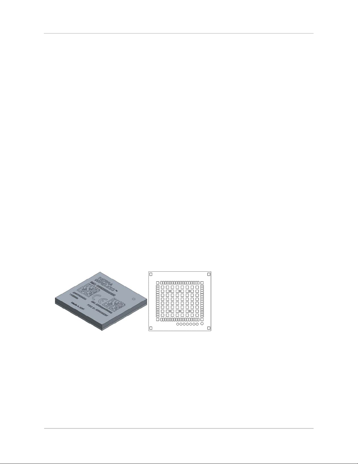
1.2. Physical Dimensions
AirPrime HL7688 modules are compact, robust, fully shielded modules with the following dimensions:
Length: 23 mm
Width: 22 mm
Thickness: 2.5 mm
Weight: 3.5 g
Note: Dimensions specified above are typical values.

4119272 Rev 2.0 August 16, 2016 11
Product Technical Specification Introduction
1.3. General Features
The table below summarizes the AirPrime HL7688 features.
Table 2. General Features
Feature Description
Physical
Small form factor (146-pad solderable LGA pad) – 23mm x 22mm x
2.5mm (nominal)
Complete body shielding
RF connection pads (RF main interface)
Baseband signals connection
Electrical Single or double supply voltage (VBATT and VBATT_PA) – 3.2V – 4.5V
RF
Quad-band LTE:
LTE B2: 1900 PCS
LTE B4: 1700 AWS
LTE B5: 850 CLR
LTE B17: 700
Dual-band UMTS:
UMTS B2: 1900 PCS
UMTS B5: 850 CLR
SIM interface
Dual SIM Single Standby (DSSS)
1.8V/3V support
SIM extraction / hot plug detection
SIM/USIM support
Conforms with ETSI UICC Specifications
Supports SIM application tool kit with proactive SIM commands
Application interface
NDIS NIC interface support (Windows XP, Windows 7, Windows 8,
Windows CE, Linux)
Multiple non-multiplexed USB channel support
Dial-up networking
USB selective suspend to maximize power savings
CMUX multiplexing over UART*
AT command interface – 3GPP 27.007 standard, plus proprietary
extended AT commands

4119272 Rev 2.0 August 16, 2016 12
Product Technical Specification Introduction
Feature Description
Protocol Stack
Single mode LTE operation:
LTE FDD, bandwidth 1.4-20 MHz
System Release: 3GPP Rel. 9
Category 1 (up to 10 Mbit/s in downlink, 5 Mbit/s in uplink)
Rx Diversity
Max modulation 64 QAM DL, 16 QAM UL
Intra-frequency and inter-frequency mobility
SMS over SGs and IMS
SON ANR
Public Warning System PWS
HSDPA (High Speed Downlink Packet Access)
Evolved High Speed Downlink Packet Access (HSDPA+)
Compliant with 3GPP Release 9
Up to Category 24 (DC, 42.2Mbps)
Continuous Packet Connectivity (CPC)
Enhance fractional DPCH
IPv6 support
HSUPA (High Speed Uplink Packet Access)
Compliant with 3GPP Release 9
Category 7 (11.5Mbps)
Robust Header Compression (RoHC)
RXDIV Performance Enhancements
Type 3i (HSDPA)
HSPA Enhancements
MAC-ehs Rel. 7
HSDPA Enhanced CELL_FACH/PCH states
HSUPA Enhanced CELL_FACH states (eFACH) Rel 8
MAC-i/is Rel.8
Serving cell change enhancements Rel. 8
SMS
SMS over SGs and IMS
SMS MO and MT
SMS saving to SIM card or ME storage
SMS reading from SIM card or ME storage
SMS sorting
SMS concatenation
SMS Status Report
SMS replacement support
SMS storing rules (support of
AT+CNMI, AT+CNMA)
4119272 Rev 2.0 August 16, 2016 13
Product Technical Specification Introduction
Feature Description
Connectivity
Multiple (up to 20) cellular packet data profiles
Sleep mode for minimum idle power draw
Mobile-originated PDP context activation / deactivation
Support QoS profile
Release 97 – Precedence Class, Reliability Class, Delay Class, Peak
Throughput, Mean Throughput
Release 99 QoS negotiation – Background, Interactive, and
Streaming
Static and Dynamic IP address. The network may assign a fixed IP
address or dynamically assign one using DHCP (Dynamic Host
Configuration Protocol).
Supports PAP and CHAP authentication protocols
PDP context type (IPv4, IPv6, IPv4v6). IP Packet Data Protocol context
RFC1144 TCP/IP header compression
Environmental
Operating temperature ranges (industrial grade):
Class A: -30°C to +70°C
Class B: -40°C to +85°C
RTC Real Time Clock (RTC) with calendar
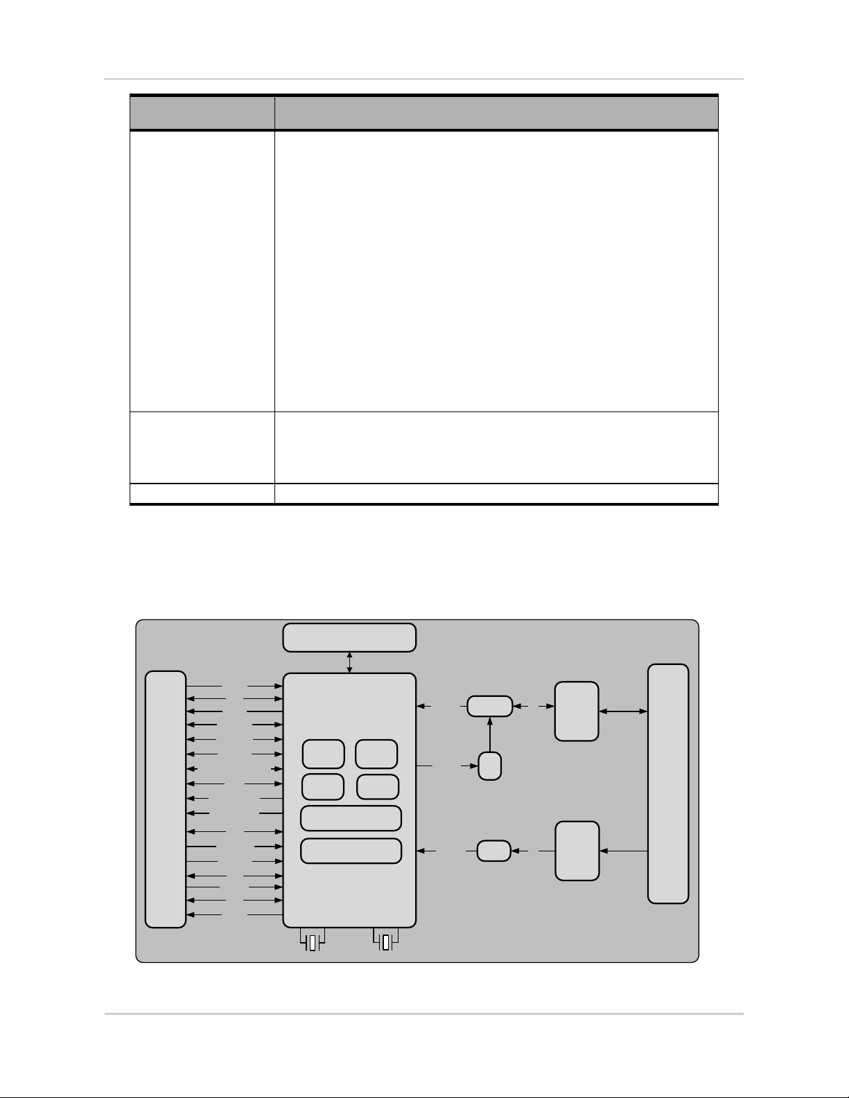
1.4. Architecture
The figure below presents an overview of the AirPrime HL7688’s internal architecture and external
interfaces.
AirPrime HL7688
Memory
(Flash + RAM)
SAW
Filters
26MHz
32.768KHz
UART x 1
Trace Debug (5 pins)
VBATT
GND
VGPIO
BAT_RTC
GPIO x 12
RESET_IN
RF Main
JTAG
LGA-
146
Baseband
SIM1
MCU DSP
PMU RF
Analog Baseband
Peripherals
LGA-
146
26M_CLKOUT
32K_CLKOUT
PWR_ON
Dulpexer
PA
USB
Antenna
Switch
Antenna
Switch
RX_LTE RF
RF DIV
T
X
_
L
T
E
RFRX_LTE
ADC x 1
PCM
TX_ON
Figure 1. Architecture Overview
4119272 Rev 2.0 August 16, 2016 14
Product Technical Specification Introduction
1.5. Interfaces
The AirPrime HL7688 module provides the following interfaces and peripheral connectivity:
1x – 8-wire UART
1x – Active Low RESET
1x – USB 2.0
1x – Backup Battery Interface
2x – System Clock Out
1x – Active Low POWER-ON
1x – 1.8V/3V SIM
1x – JTAG Interface
12x – GPIOs (2 of which have multiplexes)
1x – Main Antenna
1x – RX Diversity Antenna
1x – VGPIO
1x – TX_ON
1x – ADC
1x – PCM
1x – Debug Interface
1.6. Connection Interface
The AirPrime HL7688 module is an LGA form factor device. All electrical and mechanical connections
are made through the 146 Land Grid Array (LGA) pads on the bottom side of the PCB.
Figure 2. Mechanical Overview
The 146 pads have the following distribution:
66 inner signal pads, 1x0.5mm, pitch 0.8mm
1 reserved test point (do not connect), 1.0mm diameter
7 test point (JTAG), 0.8mm diameter, 1.20mm pitch
64 inner ground pads, 1.0x1.0mm, pitch 1.825mm/1.475mm
4 inner corner ground pads, 1x1mm
4 outer corner ground pads, 1x0.9mm
4119272 Rev 2.0 August 16, 2016 15
Product Technical Specification Introduction
1.7. ESD
Refer to the following table for ESD Specifications.
Note: Information specified in the following table is preliminary and subject to change.
Table 3. ESD Specifications
Category Connection Specification
Operational RF ports IEC-61000-4-2 – Level (Electrostatic Discharge Immunity Test)
Non-operational
Host connector
interface
Unless otherwise specified:
JESD22-A114 +/- 1kV Human Body Model
JESD22-A115 +/- 200V Machine Model
JESD22-C101C +/- 250V Charged Device Model
Signals
SIM connector
Adding ESD protection is highly recommended at the point where
the USIM contacts are exposed, and for any other signals that
would be subjected to ESD by the user.
Other host signals
1.8. Environmental and Certifications
1.8.1. Environmental Specifications
The environmental specification for both operating and storage conditions are defined in the table
below.
Table 4. Environmental Specifications
Conditions Range
Operating Class A -30°C to +70°C
Operating Class B -40°C to +85°C
Storage -40°C to +85°C
Class A is defined as the operating temperature ranges that the device:
Shall exhibit normal function during and after environmental exposure.
Shall meet the minimum requirements of 3GPP or appropriate wireless standards.
Class B is defined as the operating temperature ranges that the device:
Shall remain fully functional during and after environmental exposure
Shall exhibit the ability to establish an SMS or DATA call (emergency call) at all times even
when one or more environmental constraint exceeds the specified tolerance.
Unless otherwise stated, full performance should return to normal after the excessive
constraint(s) have been removed.
4119272 Rev 2.0 August 16, 2016 16
Product Technical Specification Introduction
1.8.2. Regulatory
The AirPrime HL7688 is compliant with FCC regulations.
FCC compliance will be reflected on the AirPrime HL7688 label.
Table 5. Regulation Compliance
Document Current Version Description
GCF-CC v3.56.1 or later GCF Conformance Certification Criteria
NAPRD.03 V5.22 or later North American Program Reference Document
FCC Part 22, 24, 27 NA Federal Communications Commission
1.8.3. RoHS Directive Compliant
The AirPrime HL7688 module is compliant with RoHS Directive 2011/65/EU which sets limits for the
use of certain restricted hazardous substances. This directive states that “from 1st July 2006, new
electrical and electronic equipment put on the market does not contain lead, mercury, cadmium,
hexavalent chromium, polybrominated biphenyls (PBB) or polybrominated diphenyl ethers (PBDE)”.
1.8.4. Disposing of the Product
This electronic product is subject to the EU Directive 2012/19/EU for Waste Electrical
and Electronic Equipment (WEEE). As such, this product must not be disposed of at a
municipal waste collection point. Please refer to local regulations for directions on how
to dispose of this product in an environmental friendly manner.
1.9. References
[1] AirPrime HL Series Customer Process Guidelines
Reference Number: 4114330
[2] AirPrime HL7688 AT Commands Interface Guide
Reference Number: TBD

4119272 Rev 2.0 August 16, 2016 17
2. Pad Definition
AirPrime HL7688 pads are divided into 3 functional categories.
Core functions and associated pads cover all the mandatory features for M2M connectivity and will be available by default across all CF
3
family of
modules. These Core functions are always available and always at the same physical pad locations. A customer platform using only these functions
and associated pads is guaranteed to be forward and/or backward compatible with the next generation of CF
3
modules.
Extension functions and associated pads bring additional capabilities to the customer. Whenever an Extension function is available on a module, it
is always at the same pad location.
Custom functions and associated pads are specific to a given module, and make an opportunistic use of specific chipset functions and I/Os.
Custom features should be used with caution as there is no guarantee that the custom functions available on a given module will be available on
other CF
3
modules.
Other pads marked as “not connected” or “reserved” should not be used.
Table 6. Pad Definition
Pad # Signal Name Function I/O
Active
Low / High
Power Supply
Domain
Recommendation
for Unused Pads
Type
1 GPIO1 General purpose input/output I/O
1.8V Left Open Extension
2
UART1_RI /
TRACE_DATA3
UART1 Ring indicator / Trace data 3 O
1.8V Connect to test point Core / Custom
3 UART1_RTS UART1 Request to send I L 1.8V Connect to test point Core
4 UART1_CTS UART1 Clear to send O L 1.8V Connect to test point Core
5 UART1_TX UART1 Transmit data I
1.8V Connect to test point Core
6 UART1_RX UART1 Receive data O
1.8V Connect to test point Core
7 UART1_DTR UART1 Data terminal ready I L 1.8V Connect to test point Core
8
UART1_DCD /
TRACE_DATA1
UART1 Data carrier detect / Trace data 1
O L 1.8V Connect to test point Core / Custom
 Loading...