

Page 1

AirPrime HL7800 and HL7800-M
Product Technical Specification
41111094
1.7
August 10, 2018
Page 2

Product Technical Specification
Important Notice
Due to the nature of wireless communications, transmission and reception of data can never be
guaranteed. Data may be delayed, corrupted (i.e., have errors) or be totally lost. Although significant
delays or losses of data are rare when wireless devices such as the Sierra Wireless modem are used
in a normal manner with a well-constructed network, the Sierra Wireless modem should not be used
in situations where failure to transmit or receive data could result in damage of any kind to the user or
any other party, including but not limited to personal injury, death, or loss of property. Sierra Wireless
accepts no responsibility for damages of any kind resulting from delays or errors in data transmitted or
received using the Sierra Wireless modem, or for failure of the Sierra Wireless modem to transmit or
receive such data.
Safety and Hazards
Do not operate the Sierra Wireless modem in areas where cellular modems are not advised without
proper device certifications. These areas include environments where cellular radio can interfere such
as explosive atmospheres, medical equipment, or any other equipment which may be susceptible to
any form of radio interference. The Sierra Wireless modem can transmit signals that could interfere
with this equipment. Do not operate the Sierra Wireless modem in any aircraft, whether the aircraft is
on the ground or in flight. In aircraft, the Sierra Wireless modem MUST BE POWERED OFF. When
operating, the Sierra Wireless modem can transmit signals that could interfere with various onboard
systems.
Note: Some airlines may permit the use of cellular phones while the aircraft is on the ground and the door
The driver or operator of any vehicle should not operate the Sierra Wireless modem while in control of
a vehicle. Doing so will detract from the driver or operator’s control and operation of that vehicle. In
some states and provinces, operating such communications devices while in control of a vehicle is an
offence.
is open. Sierra Wireless modems may be used at this time.
Limitations of Liability
This manual is provided “as is”. Sierra Wireless makes no warranties of any kind, either expressed or
implied, including any implied warranties of merchantability, fitness for a particular purpose, or
noninfringement. The recipient of the manual shall endorse all risks arising from its use.
The information in this manual is subject to change without notice and does not represent a
commitment on the part of Sierra Wireless. SIERRA WIRELESS AND ITS AFFILIATES
SPECIFICALLY DISCLAIM LIABILITY FOR ANY AND ALL DIRECT, INDIRECT, SPECIAL,
GENERAL, INCIDENTAL, CONSEQUENTIAL, PUNITIVE OR EXEMPLARY DAMAGES INCLUDING,
BUT NOT LIMITED TO, LOSS OF PROFITS OR REVENUE OR ANTICIPATED PROFITS OR
REVENUE ARISING OUT OF THE USE OR INABILITY TO USE ANY SIERRA WIRELESS
PRODUCT, EVEN IF SIERRA WIRELESS AND/OR ITS AFFILIATES HAS BEEN ADVISED OF THE
POSSIBILITY OF SUCH DAMAGES OR THEY ARE FORESEEABLE OR FOR CLAIMS BY ANY
THIRD PARTY.
Notwithstanding the foregoing, in no event shall Sierra Wireless and/or its affiliates aggregate liability
arising under or in connection with the Sierra Wireless product, regardless of the number of events,
occurrences, or claims giving rise to liability, be in excess of the price paid by the purchaser for the
Sierra Wireless product.
41111094 Rev 1.7 August 10, 2018 2
Page 3
Product Technical Specification
Patents
This product may contain technology developed by or for Sierra Wireless Inc.
This product is manufactured or sold by Sierra Wireless Inc. or its affiliates under one or more patents
licensed from MMP Portfolio Licensing.
Copyright
© 2018 Sierra Wireless. All rights reserved.
Trademarks
Sierra Wireless®, AirPrime®, AirLink®, AirVantage®, WISMO®, ALEOS® and the Sierra Wireless and
Open AT logos are registered trademarks of Sierra Wireless, Inc. or one of its subsidiaries.
Watcher® is a registered trademark of NETGEAR, Inc., used under license.
Windows® and Windows Vista® are registered trademarks of Microsoft Corporation.
Macintosh® and Mac OS X® are registered trademarks of Apple Inc., registered in the U.S. and other
countries.
QUALCOMM® is a registered trademark of QUALCOMM Incorporated. Used under license.
Other trademarks are the property of their respective owners.
Contact Information
Sales information and technical support, including
warranty and returns
Corporate and product information Web: sierrawireless.com
Web: sierrawireless.com/company/contact-us/
Global toll-free number: 1-877-687-7795
6:00 am to 5:00 pm PST
41111094 Rev 1.7 August 10, 2018 3
Page 4
Product Technical Specification
Document History
Version Date Updates
1.0 November 24, 2017 Creation
Added 3.3 Power Consumption States
Updated:
Table 2 General Features
1.1 February 01, 2018
1.2 May 04, 2018
1.3 July 05, 2018
1.4 July 10, 2018 Updated Table 10 Low Current Consumption Mode
1.5 July 25, 2018
1.6 August 10, 2018
Table 5 Pin Definition
3.2 Current Consumption
Table 11 Current Consumption Mode
3.16 Debug Interface
3.19.3 Rx Sensitivity
Added:
Table 9 Maximum Current Consumption
Updated:
GNSS to GPS
1.7 ESD Specifications
1.8.5 RoHS Directive Compliance
3.2 Current Consumption
Table 21 Digital I/O Electrical Characteristics
3.11 Power On Signal (PWR_ON_N)
3.19 RF Interface
5 Reliability Specification
Added 1.8.3 ATEX Compliance
Updated:
Table 1 Supported Bands/Connectivity
Table 2 General Features
1.5 Interfaces
Table 5 Pin Definition
Table 9 Maximum Current Consumption
3.2 Current Consumption
3.3 Power Consumption States
3.11 Power On Signal (PWR_ON_N)
3.12 Reset Signal (RESET_IN_N)
Table 40 Typical Conducted RX Sensitivity
Added:
1.8.2 Frequency Drift Correction
6 Legal Information
HL7800-M
Updated:
Table 9 Maximum Current Consumption
Moved Japan Approval to 6.1; updated Figure 16 Sample Japan
Certification Indication
Updated:
6.2 FCC Statement
6.3 IC Statement
41111094 Rev 1.7 August 10, 2018 4
Page 5

Contents
1. INTRODUCTION ................................................................................................ 10
1.1. Common Flexible Form Factor (CF3) ................................................................................ 11
1.2. Physical Dimensions ......................................................................................................... 11
1.3. General Features ............................................................................................................... 11
1.4. Architecture........................................................................................................................ 13
1.5. Interfaces ........................................................................................................................... 14
1.6. Connection Interface ......................................................................................................... 14
1.7. ESD Specifications ............................................................................................................ 15
1.8. Environmental and Certifications ....................................................................................... 15
1.8.1. Environmental Specifications ................................................................................... 15
1.8.2. Frequency Drift Correction ....................................................................................... 16
1.8.3. ATEX Compliance ................................................................................................... 16
1.8.4. Regulatory ................................................................................................................ 16
1.8.5. RoHS Directive Compliance .................................................................................... 16
1.8.6. Disposing of the Product .......................................................................................... 17
1.9. References ........................................................................................................................ 17
2. PAD DEFINITION ............................................................................................... 18
2.1. Pin Types ........................................................................................................................... 22
2.2. Pad Configuration (Top View, Through Module) ............................................................... 23
3. DETAILED INTERFACE SPECIFICATIONS ..................................................... 24
3.1. Power Supply..................................................................................................................... 24
3.2. Current Consumption ........................................................................................................ 25
3.3. Power Consumption States ............................................................................................... 26
3.3.1. 3GPP Power Saving Features ................................................................................. 26
3.3.2. Power Modes ........................................................................................................... 29
3.4. VGPIO ............................................................................................................................... 29
3.5. Real Time Clock (BAT_RTC) ............................................................................................ 30
3.6. USIM Interface ................................................................................................................... 30
3.6.1. UIM1_DET ............................................................................................................... 31
3.7. USB Interface .................................................................................................................... 32
3.8. Electrical Information for Digital I/O ................................................................................... 32
3.9. General Purpose Input/Output (GPIO) .............................................................................. 33
3.10. Main Serial Link (UART1) .................................................................................................. 33
3.10.1. 8-wire Application .................................................................................................... 34
3.10.2. 4-wire Application (TBC) .......................................................................................... 35
3.10.3. 2-wire Application (TBC) .......................................................................................... 35
3.11. Power On Signal (PWR_ON_N) ........................................................................................ 35
3.11.1. Not Managed (Default) ............................................................................................ 36
41111094 Rev 1.7 August 10, 2018 5
Page 6

Product Technical Specification
3.11.2. Managed .................................................................................................................. 37
3.12. Reset Signal (RESET_IN_N) ............................................................................................. 38
3.13. Analog to Digital Converter (ADC)..................................................................................... 39
3.14. Clock Interface ................................................................................................................... 39
3.15. PCM ................................................................................................................................... 40
3.16. Debug Interface ................................................................................................................. 40
3.17. Wake Up Signal (WAKE_UP) ............................................................................................ 40
3.18. Fast Shutdown Signal (FAST_SHUTDOWN_N) ............................................................... 41
3.19. RF Interface ....................................................................................................................... 42
3.19.1. RF Connection ......................................................................................................... 42
3.19.2. Maximum Output Power .......................................................................................... 42
3.19.3. Rx Sensitivity ........................................................................................................... 42
3.19.4. TX Indicator (TX_ON) .............................................................................................. 43
3.20. GPS Interface .................................................................................................................... 44
3.20.1. GPS Performance .................................................................................................... 44
3.20.2. GPS Antenna Indicator (EXT_LNA_GPS_EN) ........................................................ 44
4. MECHANICAL DRAWINGS ............................................................................... 45
5. RELIABILITY SPECIFICATION ......................................................................... 48
5.1. Preconditioning Test .......................................................................................................... 48
5.2. Performance Test .............................................................................................................. 48
5.3. Aging Tests ........................................................................................................................ 49
5.4. Characterization Tests ....................................................................................................... 50
6. LEGAL INFORMATION ..................................................................................... 51
6.1. Japan Radio and Telecom Approval ................................................................................. 51
6.2. FCC Statement .................................................................................................................. 51
6.2.1. Radiation Exposure Statement ................................................................................ 51
6.2.2. End Product Labeling .............................................................................................. 52
6.2.3. Manual Information to the End User ........................................................................ 53
6.3. IC Statement ...................................................................................................................... 54
6.3.1. Radiation Exposure Statement / Déclaration d'Exposition aux Radiations ............. 55
6.3.2. End Product Labeling / Plaque Signalétique du Produit Final ................................. 56
6.3.3. Manual Information to the End User / Manuel d'Information à l'Utilisateur Final ..... 56
7. ORDERING INFORMATION .............................................................................. 57
8. TERMS AND ABBREVIATIONS ........................................................................ 58
41111094 Rev 1.7 August 10, 2018 6
Page 7

List of Figures
Figure 1. Architecture Overview ..................................................................................................... 13
Figure 2. Mechanical Overview (Top View) .................................................................................... 14
Figure 3. Pad Configuration (Top View through Module) ............................................................... 23
Figure 4. PSM Example (Simplified) ............................................................................................... 26
Figure 5. eDRX Example (PTW=4) ................................................................................................ 28
Figure 6. 8-wire UART Application Example .................................................................................. 34
Figure 7. 4-wire UART Application Example .................................................................................. 35
Figure 8. 2-wire UART Application Example .................................................................................. 35
Figure 9. Power Up and Power Down Sequence without PWR_ON_N ......................................... 36
Figure 10. Power Up Sequence with PWR_ON_N Cold Start ......................................................... 37
Figure 11. Power On Sequence with PWR_ON_N .......................................................................... 37
Figure 12. TX_ON State during TX Burst ......................................................................................... 43
Figure 13. Mechanical Drawing ........................................................................................................ 45
Figure 14. Dimensions Drawing ....................................................................................................... 46
Figure 15. Footprint Drawing ............................................................................................................ 47
Figure 16. Sample Japan Certification Indication ............................................................................. 51
41111094 Rev 1.7 August 10, 2018 7
Page 8

List of Tables
Table 1. Supported Bands/Connectivity ........................................................................................ 10
Table 2. General Features ............................................................................................................ 11
Table 3. Environmental Specifications .......................................................................................... 15
Table 4. Values for ATEX Compliance .......................................................................................... 16
Table 5. Pin Definition ................................................................................................................... 18
Table 6. Pin Type Codes ............................................................................................................... 22
Table 7. Power Supply Pin Description ......................................................................................... 24
Table 8. Power Supply Electrical Characteristics .......................................................................... 24
Table 9. Maximum Current Consumption...................................................................................... 24
Table 10. Low Current Consumption Mode ..................................................................................... 25
Table 11. Current Consumption Mode ............................................................................................ 26
Table 12. eDRX-Related Commands .............................................................................................. 28
Table 13. Low Power Modes ........................................................................................................... 29
Table 14. VGPIO Pin Description .................................................................................................... 30
Table 15. VGPIO Electrical Characteristics ..................................................................................... 30
Table 16. BAT_RTC Electrical Characteristics................................................................................ 30
Table 17. USIM1 Pin Description .................................................................................................... 31
Table 18. USIM1 Electrical Characteristics ..................................................................................... 31
Table 19. USB Pin Description ........................................................................................................ 32
Table 20. USB Electrical Characteristics ......................................................................................... 32
Table 21. Digital I/O Electrical Characteristics ................................................................................ 32
Table 22. GPIO Pin Description ...................................................................................................... 33
Table 23. UART1 Pin Description ................................................................................................... 34
Table 24. PWR_ON_N Pin Description ........................................................................................... 36
Table 25. PWR_ON_N Electrical Characteristics ........................................................................... 36
Table 26. PWR_ON_N Not Managed Timing.................................................................................. 36
Table 27. PWR_ON_N Managed Timing ........................................................................................ 38
Table 28. RESET_IN_N Pin Description ......................................................................................... 38
Table 29. RESET_IN_N Electrical Characteristics .......................................................................... 38
Table 30. ADC Pin Description ........................................................................................................ 39
Table 31. ADC Electrical Characteristics ........................................................................................ 39
Table 32. Clock Interface Pin Description ....................................................................................... 40
Table 33. Debug Pin Description ..................................................................................................... 40
Table 34. WAKE_UP Pin Description .............................................................................................. 40
Table 35. WAKE_UP Electrical Characteristics .............................................................................. 41
Table 36. FAST_SHUTDOWN_N Pin Description .......................................................................... 41
Table 37. FAST_SHUTDOWN_N Electrical Characteristics ........................................................... 41
41111094 Rev 1.7 August 10, 2018 8
Page 9

Product Technical Specification
Table 38. RF Main Pin Description .................................................................................................. 42
Table 39. Maximum Output Power .................................................................................................. 42
Table 40. Typical Conducted RX Sensitivity ................................................................................... 42
Table 41. TX_ON Pin Description ................................................................................................... 43
Table 42. TX_ON Characteristics .................................................................................................... 44
Table 43. GPS Antenna Specifications ........................................................................................... 44
Table 44. GPS Performance ........................................................................................................... 44
Table 45. Preconditioning Test ........................................................................................................ 48
Table 46. Performance Test ............................................................................................................ 48
Table 47. Aging Tests ...................................................................................................................... 49
Table 48. Characterization Tests .................................................................................................... 50
Table 49. Ordering Information ....................................................................................................... 57
41111094 Rev 1.7 August 10, 2018 9
Page 10
1. Introduction
This document is the Product Technical Specification for the AirPrime HL7800 and HL7800-M
Embedded Modules designed for M2M and Internet of Things (IoT) markets. It defines the high-level
product features and illustrates the interfaces for these features. This document is intended to cover
the hardware aspects of the product, including electrical and mechanical.
The AirPrime HL7800 and HL7800-M modules belongs to the AirPrime HL Series from Essential
Connectivity Module family. These are industrial grade Embedded Wireless Modules that provides
data connectivity on LTE (as listed in Table 1 Supported Bands/Connectivity).
The AirPrime HL7800 and HL7800-M modules supports a large variety of interfaces such as USB FS,
UART, ADC, and GPIOs to provide customers with the highest level of flexibility in implementing highend solutions.
Table 1. Supported Bands/Connectivity
Transmit Band (Tx) Receive Band (Rx)
LTE Band
Minimum Maximum Minimum Maximum
B1 1920 MHz 1980 MHz 2110 MHz 2170 MHz
B2 1850 MHz 1910 MHz 1930 MHz 1990 MHz
B3 1710 MHz 1785 MHz 1805 MHz 1880 MHz
B4 1710 MHz 1755 MHz 2110 MHz 2155 MHz
B5 824 MHz 849 MHz 869 MHz 894 MHz
B8 880 MHz 915 MHz 925 MHz 960 MHz
B9 1749.9 MHz 1784.9 MHz 1844.9 MHz 1879.9 MHz * *
B10 1710 MHz 1770 MHz 2110 MHz 2170 MHz * *
B12 699 MHz 716 MHz 729 MHz 746 MHz
B13 777 MHz 787 MHz 746 MHz 756 MHz
B14 788 MHz 798 MHz 758 MHz 768 MHz
B17 704 MHz 716 MHz 734 MHz 746 MHz *
B18 815 MHz 830 MHz 860 MHz 875 MHz
B19 830 MHz 845 MHz 875 MHz 890 MHz
B20 832 MHz 862 MHz 791 MHz 821 MHz
B25 1850 MHz 1915 MHz 1930 MHz 1995 MHz
B26 814 MHz 849 MHz 859 MHz 894 MHz
B27 807 MHz 824 MHz 852 MHz 869 MHz
B28 703 MHz 748 MHz 758 MHz 803 MHz
B66 1710 MHz 1780 MHz 2110 MHz 2200 MHz
Cat-M1
(HL7800
and
HL7800-M)
Cat-NB1
(HL7800
only)
*
*
*
* Will be supported in a future release.
Note: RF bands supported are configurable through AT command. The software-based radio allows for
the ability to support extra bands for worldwide connectivity.
41111094 Rev 1.7 August 10, 2018 10
Page 11

Product Technical Specification Introduction
1.1. Common Flexible Form Factor (CF3)
The AirPrime HL7800 and HL7800-M modules belong to the Common Flexible Form Factor
(CF3) family of modules. This family consists of a series of WWAN modules that share the same
mechanical dimensions (same width and length with varying thicknesses) and footprint. The CF
factor provides a unique solution to a series of problems faced commonly in the WWAN module space
as it:
Accommodates multiple radio technologies (LTE advanced) and band groupings.
Supports bit-pipe (Essential Module Series) and value add (Smart Module Series) solutions.
Offers electrical and functional compatibility.
Provides Direct Mount as well as Socketability depending on customer needs.
3
form
1.2. Physical Dimensions
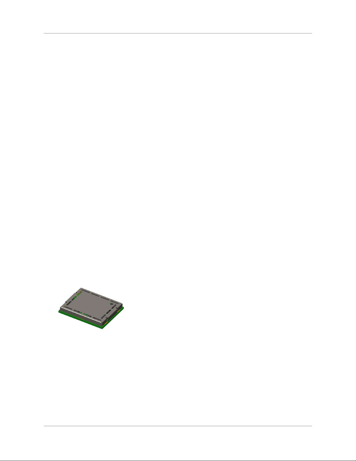
AirPrime HL7800 and HL7800-M modules are compact, robust, fully shielded modules with the
following dimensions:
Length: 18.0 mm
Width: 15.0 mm
Thickness: 2.4 mm
Weight: 1.17 g
Note: Dimensions specified above are typical values.
1.3. General Features
The table below summarizes the AirPrime HL7800 and HL7800-M’s features.
Table 2. General Features
Feature Description
Small form factor (86-pad solderable LGA pad) – 15.0mm x 18.0mm x
2.4mm (nominal)
Physical
Power supply Single or double supply voltage (VBATT and VBATT_PA) – 3.2V – 4.35V
Metal shield can
RF connection pads (RF main and RF GPS)
Baseband signals connection
41111094 Rev 1.7 August 10, 2018 11
Page 12

Product Technical Specification Introduction
Feature Description
Cat-M1
Power Class 3 (23dBm)
Software based radio allowing support of extra bands for worldwide
operation (will be supported in a future release)
Cat-NB1 (not supported on the HL7800-M)
Power Class 3 (23dBm)
RF
Software based radio allowing support of extra bands for worldwide
operation (will be supported in a future release)
GPS*
1575.42 MHz
SIM interface
Application interface
Protocol stack
Protocol stack
Note: The GPS receiver shares
The end-device target should allow GPS positioning for asset
management applications where infrequent and no real-time position
updates are required.
1.8V only support (3V SIM is not supported)
SIM extraction / hot plug detection
SIM/USIM support
Conforms with ETSI UICC Specifications.
Supports SIM application tool kit with proactive SIM commands
AT command interface – 3GPP 27.007 standard, plus proprietary extended
AT commands
CMUX multiplexing over UART
USB FS*
Cat-M1
3GPP Rel. 13
Half-duplex
Channel bandwidth 1.4MHz
LTE carrier bandwidth 1.4 / 3 / 5 / 10 / 15 / 20 MHz
Up to 375kbit/s uplink, 300 kbit/s downlink
Extended Coverage Mode A
PSM (Power Save Mode)
I-DRX
C-DRX
Idle mode mobility
Connected mode mobility
eDRX (Extended Discontinuous Reception)
CiOT optimizations (U-Plane, C-Plan)*
Cat-NB1* (not supported on the HL7800-M)
3GPP Rel. 13
Half-duplex
Channel bandwidth 180KHz
LTE carrier bandwidth 1.4 / 3 / 5 / 10 / 15 / 20 MHz
Up to 100 kbit/s in downlink
Operational mode – Inband, Guard band, Standalone
CioT EPS optimizations (Data over NAS)
Extended coverage
Flexible selection
Manual system selection across RATs
Dynamic system selection across RATs (preferred RAT)*
the
same RF resources as the 4G receiver.
41111094 Rev 1.7 August 10, 2018 12
Page 13
Product Technical Specification Introduction
Feature Description
SMS over SG
SMS
Connectivity
Environmental
RTC Real Time Clock (RTC)
* Will be available in a future release.
MO/MT
SMS storage to SIM card or ME storage
Multiple cellular packet data profiles
Sleep mode for minimum idle power draw
Mobile-originated PDP context activation / deactivation
Static and Dynamic IP address. The network may assign a fixed IP address
or dynamically assign one using DHCP (Dynamic Host Configuration
Protocol).
PDP context type (IPv4, IPv6, IPv4v6). IP Packet Data Protocol context
RFC1144 TCP/IP header compression
Operating temperature ranges (industrial grade):
Class A: -30°C to +70°C
Class B: -40°C to +85°C
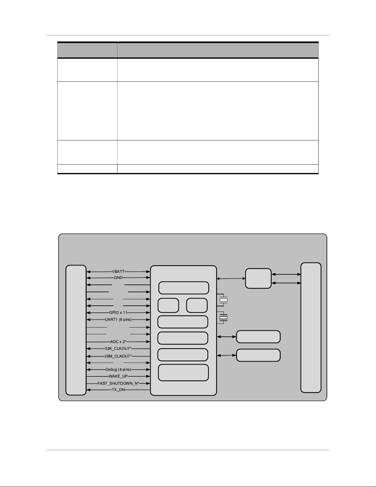
1.4. Architecture
The figure below presents an overview of the AirPrime HL7800 and HL7800-M’s internal architecture
and external interfaces.
AirPrime HL7800 and HL7800-M
Baseband/Transceiver
RF 4G
LGA-
86
VGPIO
BAT_RTC*
USIM
USB*
PWR_ON_N
RESET_IN_N
PCM*
Transceiver
MCU DSP
PMU
Analog Baseband
Peripherals
RAM Memory
TX FEM
32.768KHz
26MHz
Embedded SIM
Flash Memory
RF GPS*
LGA-
86
* Will be available in a future release
Figure 1. Architecture Overview
41111094 Rev 1.7 August 10, 2018 13
Page 14
Product Technical Specification Introduction
1.5. Interfaces
The AirPrime HL7800 and HL7800-M modules provide the following interfaces and peripheral
connectivity:
1x – VGPIO (1.8V)
1x – BAT_RTC backup battery interface (will be available in a future release)
1x – 1.8V USIM
1x – USB FS (will be available in a future release)
11x – GPIOs
1x – 8-wire UART
1x – Active Low POWER ON (will be available in a future release)
1x – Active Low RESET
2x – ADC (will be available in a future release)
2x – System clock out (32.768 KHz and 26 MHz) (will be available in a future release)
1x – PCM (will be available in a future release)
1x – 4-wire UART for debug interface only
1x – Wake up signal
1x – Fast shutdown signal (will be available in a future release)
1x – Main RF Antenna
1x – TX indicator
1x – GPS Antenna (will be available in a future release)
1.6. Connection Interface
AirPrime HL7800 and HL7800-M modules are LGA form factor devices. All electrical and mechanical
connections are made through the 86 Land Grid Array (LGA) pads on the bottom side of the PCB.
Figure 2. Mechanical Overview (Top View)
The 86 pads have the following distribution:
66 inner signal pads, 1x0.5mm, pitch 0.8mm
16 inner ground pads, 1.0x1.0mm, pitch 1.825mm/1.475mm
4 outer corner ground pads, 0.85x0.97mm
41111094 Rev 1.7 August 10, 2018 14
Page 15
Product Technical Specification Introduction
1.7. ESD Specifications
IEC-61000-4-2 (test carried out on test vehicle including ESD protection)
Contact Voltage: ±2kV, ±4kV, ±6kV (design target)
Air Voltage: ±2kV, ±4kV, ±8kV (design target)
Unless otherwise specified:
JESD22-A114 ± 250kV Human Body Model
JESD22-C101C ± 250V Charged Device Model
1.8. Environmental and Certifications
1.8.1. Environmental Specifications
The environmental specification for both operating and storage conditions are defined in the table
below.
Table 3. Environmental Specifications
Conditions Range
Operating Class A -30°C to +70°C
Operating Class B -40°C to +85°C
Storage -40°C to +85°C
Class A is defined as the operating temperature ranges that the device:
Shall exhibit normal function during and after environmental exposure.
Shall meet the minimum requirements of 3GPP or appropriate wireless standards.
Class B is defined as the operating temperature ranges that the device:
Shall remain fully functional during and after environmental exposure
Shall exhibit the ability to establish an SMS or DATA call (emergency call) at all times even
when one or more environmental constraint exceeds the specified tolerance.
Unless otherwise stated, full performance should return to normal after the excessive
constraint(s) have been removed.
41111094 Rev 1.7 August 10, 2018 15
Page 16
Product Technical Specification Introduction
1.8.2. Frequency Drift Correction
The HL7800 and HL7800-M are environmental sensitive and able to correct temperature and aging
effects automatically. Parameters to be considered when addressing the environmental effect on the
HL7800 and HL7800-M are as follows:
Maximum deviation correction: 20 ppm
Environmental Temperature effect: 0.5 ppm
Factory reflow effect: 1 ppm + 1 ppm / reflow
Aging effect: 1 ppm /year of use
For example, if an HL7800 module is mounted on a single side (1 reflow) customer PCB and used for
10 years between -40 and +85°C, the frequency drift will be up to 0.5 + (1 + 1) + (1 * 10) = 12.5 ppm,
which is in the limits of the 20 ppm maximum correction.
1.8.3. ATEX Compliance
The following table lists the inductor and capacitor values to be considered for ATEX certification of
the system hosting the HL7800 and HL7800-M modules. All supplies in the modules are linear LDO
except for one 1.3V DC/DC step-down.
Table 4. Values for ATEX Compliance
Parameter Valu e Tolerance
Total Inductance 2.21 µH 30%
Total Capacitance 43.64 µF 20 %
1.8.4. Regulatory
The AirPrime HL7800 and HL7800-M modules will be compliant with the following regulations:
RED
FCC
IC
RCM
JRF/JPA
1.8.5. RoHS Directive Compliance
AirPrime HL7800 and HL7800-M modules are compliant with RoHS Directive 2011/65/EU, including
directive 2015/863 amending annex II, which sets limits for the use of certain restricted hazardous
substances. This directive states that electrical and electronic equipment put on the market does not
contain lead, mercury, cadmium, hexavalent chromium, polybrominated biphenyls (PBB),
polybrominated diphenyl ethers (PBDE), Bis (2-ethylhexyl) phthalate (DEHP), Butyl benzyl phthalate
(BBP), Dibutyl phthalate (DBP) or Diisobutyl phthalate (DIBP) above threshold limits.
41111094 Rev 1.7 August 10, 2018 16
Page 17

Product Technical Specification Introduction
1.8.6. Disposing of the Product
This electronic product is subject to the EU Directive 2012/19/EU for Waste Electrical
and Electronic Equipment (WEEE). As such, this product must not be disposed of at a
municipal waste collection point. Please refer to local regulations for directions on how
to dispose of this product in an environmental friendly manner.
1.9. References
[1] AirPrime HL78xx Customer Process Guidelines
Reference Number: 41112095
[2] AirPrime HL78xx AT Commands Interface Guide
Reference Number: 41111821
[3] AirPrime HL Series Development Kit User Guide
Reference Number: 4114877
[4] AirPrime HL7800 Low Power Modes Application Note
Reference Number: 41112578
41111094 Rev 1.7 August 10, 2018 17
Page 18
2. Pad Definition
AirPrime HL7800 and HL7800-M pins are divided into 2 functional categories.
Core functions and associated pins cover all the mandatory features for M2M connectivity and will be available by default across all CF3 family of
modules. These Core functions are always available and always at the same physical pad locations. A customer platform using only these functions
and associated pads are guaranteed to be forward and/or backward compatible with the next generation of CF3 modules.
Extension functions and associated pins bring additional capabilities to the customer. Whenever an Extension function is available on a module, it
is always at the same pad location.
Other pins marked as “not connected” or “reserved” should not be used.
Table 5. Pin Definition
Pad # Signal Name Function I/O
C1 GPIO1 General purpose input/output I/O PU 1.8V Left Open Extension
C2 UART1_RI UART1 Ring indicator O PU 1.8V Connect to test point Core
C3 UART1_RTS UART1 Request to send I PU 1.8V Connect to test point Core
C4 UART1_CTS UART1 Clear to send O PU 1.8V Connect to test point Core
C5 UART1_TX UART1 Transmit data I PU 1.8V Connect to test point Core
C6 UART1_RX UART1 Receive data O PU 1.8V Connect to test point Core
C7 UART1_DTR UART1 Data terminal ready I PU 1.8V Connect to test point Core
C8 UART1_DCD UART1 Data carrier detect O PU 1.8V Connect to test point Core
C9 UART1_DSR UART1 Data set ready O PU 1.8V Connect to test point Core
C10 GPIO2 General purpose input/output I/O PD 1.8V Connect to test point Core
C11 RESET_IN_N Input reset signal I 1.8V Left Open Core
C12 USB_D- USB Data Negative (Full Speed) I/O 3.3V Connect to test point Extension
C13 USB_D+ USB Data Positive (Full Speed) I/O 3.3V Connect to test point Extension
Pre and Post
Reset State*
Power Supply
Domain
Recomm endation
for Unused Pads
Type
41111094 Rev 1.7 August 10, 2018 18
Page 19

Product Technical Specification Pad Definition
Pad # Signal Name Function I/O
C14 NC Not Connected Left Open Not connected
C15 NC Not Connected Left Open Not connected
C16 USB_VBUS USB VBUS I 5V Connect to test point Extension
C17 NC Not Connected Left Open Not connected
C18 NC Not Connected Left Open Not connected
C19 NC Not Connected Left Open Not Connected
C20 NC Not Connected Left Open Not Connected
C21 BAT_RTC Power supply for RTC backup I Left Open Extension
C22 26M_CLKOUT 26M System Clock Output O PD 1.8V Left Open Extension
C23 32K_CLKOUT 32.768kHz System Clock Output O PU 1.8V Left Open Extension
C24 ADC1 Analog to digital converter I 1.2V Left Open Extension
C25 ADC0 Analog to digital converter I 1.2V Left Open Extension
C26 UIM1_VCC 1.8V USIM1 Power supply O 1.8V Mandatory connection Core
C27 UIM1_CLK 1.8V USIM1 Clock O 1.8V Mandatory connection Core
C28 UIM1_DATA 1.8V USIM1 Data I/O 1.8V Mandatory connection Core
C29 UIM1_RESET 1.8V USIM1 Reset O 1.8V Mandatory connection Core
C30 GND Ground 0V 0V Mandatory connection Extension
C31 NC Not Connected Not connected
C32 GND Ground 0V 0V Mandatory connection Extension
C33 PCM_OUT PCM data out O PU 1.8V Left Open Extension
C34 PCM_IN PCM data in I PU 1.8V Left Open Extension
C35 PCM_SYNC PCM sync out I/O PU 1.8V Left Open Extension
C36 PCM_CLK PCM clock I/O PD 1.8V Left Open Extension
C37 GND Ground 0V 0V Mandatory connection Core
C38 RF_GPS RF_GPS Left Open Core
C39 GND Ground 0V 0V Mandatory connection Core
C40 GPIO7 General purpose input/output I/O PU 1.8V Left Open Core
Pre and Post
Reset State*
Power Supply
Domain
Recomm endation
for Unused Pads
Type
41111094 Rev 1.7 August 10, 2018 19
Page 20

Product Technical Specification Pad Definition
Pad # Signal Name Function I/O
C41 GPIO8 General purpose input/output I/O PD 1.8V Left Open Core
C42 NC Not Connected Not connected
C43 EXT_LNA_GPS_EN External GPS LNA enable PU Left Open Extension
C44 WAKE_UP Wake up signal I PD 1.8V Mandatory connection Extension
C45 VGPIO GPIO voltage output O 1.8V Left Open Core
C46 GPIO6 General purpose input/output I/O PD 1.8V Left Open Core
C47 NC Not Connected Left Open Not connected
C48 GND Ground 0V 0V Mandatory connection Core
C49 RF_MAIN RF Input/output Mandatory connection Core
C50 GND Ground 0V 0V Mandatory connection Core
C51 GPIO14 General purpose input/output I/O PU 1.8V Left Open Extension
C52 GPIO10 General purpose input/output I/O PU 1.8V Left Open Extension
C53 GPIO11 General purpose input/output I/O PU 1.8V Left Open Extension
C54 GPIO15 General purpose input/output I/O PU 1.8V Left Open Extension
C55 UART0_RX Debug Receive data O PU 1.8V Mandatory connection Extension
C56 UART0_TX Debug Transmit data I PU 1.8V Mandatory connection Extension
C57 UART0_CTS Debug Clear to Send O PU 1.8V Mandatory connection Extension
C58 UART0_RTS Debug Request to Send I PD 1.8V Mandatory connection Extension
C59 PWR_ON_N Active Low Power On control signal I 1.8V Mandatory connection Core
C60 TX_ON TX transmission indication O PU 1.8V Left Open Extension
C61 VBATT_PA
C62 VBATT_PA
Power supply (refer to section 3.1
Power Supply for more information)
Power supply (refer to section 3.1
Power Supply for more information)
I
I
Pre and Post
Reset State*
Power Supply
Domain
3.2V (min)
3.7V (typ)
4.35V (max)
3.2V (min)
3.7V (typ)
4.35V (max)
Recomm endation
for Unused Pads
Mandatory connection Core
Mandatory connection Core
Type
41111094 Rev 1.7 August 10, 2018 20
Page 21

Product Technical Specification Pad Definition
Pad # Signal Name Function I/O
C63 VBATT
C64 UIM1_DET / GPIO3
C65 FAST_SHUTDOWN_N Fast Shutdown signal I PU 1.8V Left Open Extension
C66 GPIO5 General purpose input/output I/O PU 1.8V Left Open Extension
CG1 – CG4,
G1 – G16
* This refers to the state before and after RESET_IN_N; state is Undefined during reset. Refer to section 3.12 Reset Signal (RESET_IN_N) for more details.
GND Ground GND 0V Core
Power supply (refer to section 3.1
Power Supply for more information)
USIM1 Detection / General purpose
input/output
I
I/O PD 1.8V Left Open Core
Pre and Post
Reset State*
Power Supply
Domain
3.2V (min)
3.7V (typ)
4.35V (max)
Recomm endation
for Unused Pads
Mandatory connection Core
Type
41111094 Rev 1.7 August 10, 2018 21
Page 22

Product Technical Specification Pad Definition
2.1. Pin Types
Table 6. Pin Type Codes
Type Definition
I Digital Input
O Digital Output
I/O Digital Input / Output
L Active High
H Active Low
T Tristate
T/PU Tristate with pull-up enabled
T/PD Tristate with pull-down enabled
PU Pull-up enabled
PD Pull-down enabled
N/A Not Applicable
41111094 Rev 1.7 August 10, 2018 22
Page 23

Product Technical Specification Pad Definition
2.2. Pad Configuration (Top View, Through Module)
Note: The following diagram shows the pad configuration from DV2 onwards.
Core pin
GND
GPIO10
GPIO11
GPIO15
UART0_RX
UART0_TX
UART0_CTS
UART0_RTS
POWER_ON_N
TX_ON
VBATT_PA
VBATT_PA
VBATT
UIM1_DET/ GPIO3
FAST_SHUTDOWN_N
GPIO5
WAKE_UP
EXT_LNA_GPS_EN
VGPIO
GPIO6
NC
GND
GND
RF_MAIN
GPIO14
CG4 CG3
C52
C53
C54
C55
C56
C57
C58
C59
C60
C61
C62
C63
C64
C65
C66
CG1 CG2
C51
C50
C49
C48
C47
C46
C45
C44
C43
G13 G15 G16
G14
G9 G10 G11 G12
GND
G5 G6 G7 G8
G1 G3 G4
G2
C1
C2
C3
C4
C5
C6
C7
C8
C9
GPIO7
GPIO8
NC
C42
C41
C40
C10
C11
C12
GND
RF_GPS
GND
C39
C38
C37
C13
C14
C15
PCM_IN
PCM_SYNC
PCM_CLK
C33
C32
C31
C30
C29
C28
C27
C26
C25
C24
C23
C22
C21
C20
C19
GND
PCM_OUT
GND
NC
GND
UIM1_RESET
UIM1_DATA
UIM1_CLK
UIM1_VCC
ADC0
ADC1
32K_CLKOUT
26M_CLKOUT
BAT_RTC
NC
NC
GNDGND
C36
C35
C34
C16
C17
C18
Extension pin
GPIO1
UART1_RI
UART1_TX
UART1_RX
UART1_CTS
UART1_RTS
UART1_DTR
GPIO2
USB_D-
USB_D+
UART1_DSR
UART1_DCD
RESET_IN_N
NC
NC
NC
NC
USB_VBUS
Figure 3. Pad Configuration (Top View through Module)
41111094 Rev 1.7 August 10, 2018 23
Page 24

3. Detailed Interface Specifications
Note: If not specified, all electrical values are given for VBATT=3.7V and an operating temperature of
25°C.
For standard applications, VBATT and VBATT_PA must be tied externally to the same power
supply. For some specific applications, AirPrime HL7800 and HL780-M modules support separate
VBATT and VBATT_PA connection if requirements below are fulfilled.
3.1. Power Supply
The AirPrime HL7800 and HL7800-M modules are supplied through the VBATT and VBATT_PA
signals.
Refer to the following table for the pin description of the Power Supply interface.
Table 7. Power Supply Pin Description
Pad Number Signal Name I/O Descripti on
C63 VBATT I Power supply (base band)
C61, C62 VBATT_PA I Power supply (radio frequency)
CG1 – CG4, G1 – G16 GND Ground
Refer to the following table for the electrical characteristics of the Power Supply interface.
Table 8. Power Supply Electrical Characteristics
Supply Minimum Typical Maximum
VBATT voltage (V) 3.2 3.7 4.35
VBATT_PA voltage (V) Full Specification 3.2 3.7 4.35
VBATT_PA voltage (V) Extended Range 2.8* (TBC) 3.7 4.35
* No guarantee of 3GPP performances over extended range.
Table 9. Maximum Current Consumption
Supply Maximum
VBATT 500mA
VBATT_PA 500mA
Note: If a single PSU is used, the recommended power supply capability is 500 mA + 500 mA = 1A.
41111094 Rev 1.7 August 10, 2018 24
Page 25

Product Technical Specification Detailed Interface Specifications
3.2. Current Consumption
The following tables list the current consumption of the AirPrime HL7800 and HL7800-M modules at
different conditions.
Note: Typical values are defined for VBATT/VBATT_PA at 3.7V and 25°C, for 50Ω impedance at all RF
Table 10. Low Current Consumption Mode
Parameter Typi cal Unit
Off mode (module switched off & VBATs Connected) 3 µA
PSM Floor in Hibernate mode 3 µA
PSM 1h in Hibernate mode 70 µA
PSM 24h in Hibernate mode 6 µA
DRX 1.28 s in Sleep mode
DRX 2.56 s in Sleep mode
eDRX 20.48 s / PTW 1 in Hibernate mode
eDRX 81.92 s / PTW 1 in Hibernate mode
* Enhancement will be available in a future firmware version.
** Values are PTW and DRX dependent.
ports. Maximum values are provided for VSWR2.5:1 (TBC) with worst conditions among supported
ranges of voltages and temperature.
3.4
1.8*
3.0
1.5*
200**
<100*
100**
<50*
mA
mA
µA
µA
Refer to section 3.3.2 Power Modes for details regarding different low power modes.
The PSM 1h and 24h in Hibernate mode assume the following conditions:
Cat-M1
Good channel conditions without UICC / USIM current
Static scenario, no repetitions
Cycle includes boot, cell acquisition, network attachment, wait for timer expiry and back to
sleep
The PSM Floor in Hibernate mode assumes the following conditions:
I/Os are not held (VGPIO is off)
Customer application is not allowed to drive the module’s I/Os
UICC / USIM is off
The module only wakes up by a high level on the WAKE_UP pin
41111094 Rev 1.7 August 10, 2018 25
Page 26

Product Technical Specification Detailed Interface Specifications
Table 11. Current Consumption Mode
Parameter Band Output Power
LTE connected mode Cat-M1 1, 2, 3, 4, 66
LTE connected mode Cat-M1
5, 8, 12, 13, 14, 18,
19, 20, 26, 28
LTE connected mode Cat-NB1 1, 3
LTE connected mode Cat-NB1 5, 8, 20, 28
23dBm 220 (TBC) mA
0dBm 110 (TBC) mA
23dBm 220 (TBC) mA
0dBm 110 (TBC) mA
23dBm 220 (TBC) mA
0dBm 110 (TBC) mA
23dBm 220 (TBC) mA
0dBm 110 (TBC) mA
Average Current
(Typical Val ues)
Unit
3.3. Power Consumption States
3.3.1. 3GPP Power Saving Features
3.3.1.1. Power Saving Mode (PSM)
Power Saving Mode (PSM) is a 3GPP feature that allows the HL7800 and HL7800-M to minimize
power consumption by registering on a PSM-supporting LTE network, entering PSM (a very low
power ‘dormant’ state) for a pre-configured duration (via a TAU (Tracking Area Update) timer), and
then waking for a short period to transmit or receive data before re-entering PSM. During the dormant
period, the module remains unreachable by the network until woken by the TAU timer or WAKE_UP
pin.
While the HL7800 or HL7800-M is in PSM:
Power consumption is significantly reduced with longer dormant periods
Networking layer signaling overhead is reduced
Radio resource signaling is reduced
Note: Simplified current consumption
pattern to illustrate general structure of
PSM cycle power state transitions.
Module transmits TAU and
exchanges data with network
Data
Idle window — Module waits for Rx
Tx
Power
off
Idle
(Active timer
(T3324))
Module returns to
dormant state,
PSM cycle repeats
registered on
Current (not to scale)
Module
network
1. User enables PSM.
2. Module requests user-specified TAU-timer period.
3. Network responds with actual TAU-timer period to use.
4. Module enters and stays in idle mode until idle mode
remains uninterrupted for the Active timer duration.
Wake event:
- TAU timer expires
- WAKE_UP Pin before timer
expires
Module enters PSM
(Dormant, very low
power)
Periodic TAU — PSM
Cycle Timer (T3412)
PSM Cycle
Idle
(Active timer
(T3324))
Power
off
Power
up
TAU
procedure
Figure 4. PSM Example (Simplified)
41111094 Rev 1.7 August 10, 2018 26
Time
Page 27

Product Technical Specification Detailed Interface Specifications
Typical candidates for PSM are systems (such as monitors and sensors) that:
Require long battery life (low power consumption)
Tolerate very long latency for mobile-terminated SMS/data
Do not use mobile-terminated voice
Send and/or receive data infrequently and periodically (e.g. on a given schedule of once
every few hours, days, weeks, etc.)
The following example describes how the module uses PSM (as shown in Figure 4 PSM Example
(Simplified)):
1. Module registers on an LTE network.
2. User enables PSM via +CPSMS, specifying the desired TAU timer and Active timer periods.
3. Module submits the PSM request (including desired TAU timer) to the network.
4. Network responds and indicates whether PSM is supported and (if it is) indicates the actual
TAU timer to use.
5. If the network supports PSM:
a. Module enters idle mode (waiting for Rx from network).
b. When module has remained idle for the Active timer period, module powers off (except for
maintaining timer and interrupts) and enters PSM.
c. Module remains in PSM for the specified TAU timer period or until the WAKEUP pin
wakes it.
d. Module powers up, then transmits TAU and exchanges data with network.
e. Module enters idle mode and cycle repeats.
Note that:
The PSM Periodic-TAU timer and Active Time values must be carefully selected to match the
intended use case(s) for the module:
Periodic TAU PSM Cycle timer (T3412) – Note that while the module is dormant (for the
duration of this timer, unless woken by the WAKE_UP pin, it will be completely
unreachable by the network.
Active Time (Idle mode time after transmission (T3324)) – Make sure to set the Active
timer high enough to provide appropriate delay-tolerance for mobile-terminated/network-
originated transmissions to be received.
When using multiple devices, consider scheduling the modules to wake at different times so
that the network does not get flooded by all modules waking and transmitting simultaneously.
41111094 Rev 1.7 August 10, 2018 27
Page 28

Product Technical Specification Detailed Interface Specifications
3.3.1.2. Extended DRX (eDRX)
The HL7800 and HL7800-M support eDRX, which is a “flexible sleep” active mode that allows for
longer sleep duration (T
DRX. The eDRX feature allows the module to not monitor every Paging Occasion (PO), but only the
POs that belong to the Paging Transmission Window (PTW) as described in the figure below.
) and a significant decrease in power consumption compared to regular
I-eDRX
Device in
C-DRX
mode
Current
T
I-DRX
Paging
Occurence
PTW=4
Current
Figure 5. eDRX Example (PTW=4)
Very long sleep duration
T
I-eDRX
Idle DRX
(I-DRX)
Paging
Occurence
Idle eDRX
(I-eDRX)
The following table describes available methods for configuring eDRX.
Table 12. eDRX-Related Commands
AT Command Description
AT+CEDRXS
AT+CEDRXRDP
Enable/disable eDRX and configure related settings
Display current eDRX settings
For example:
Time
Time
Use the AT+CEDRXS command to configure the desired T
I-eDRX
value.
During the network attachment or TAU process:
eDRX request and settings are sent to the network.
Network responds and indicates whether eDRX is supported for the connection and may
adjust the eDRX parameters.
If eDRX is supported by the network, the module only listens to paging during paging
occurrence and may enter low power mode between paging occurrence.
Note that:
Sleep duration must be carefully selected to match the intended use case(s) for the module.
While the module is asleep, it will be unreachable by the network. The duration should provide
appropriate delay-tolerance for mobile-terminated/network-originated transmissions to be
received.
Network-side store and forward is supported – Packets will be stored until the module is
reachable.
41111094 Rev 1.7 August 10, 2018 28
Page 29

Product Technical Specification Detailed Interface Specifications
3.3.2. Power Modes
Three low power modes are supported on the AirPrime HL7800 and HL7800-M modules:
Sleep Mode: 26Mhz system clock is OFF, all memories and I/O states are retained. The
module can wake-up via the WAKE_UP signal or UART1_DTR.
Lite Hibernate mode: RTC, I/O states and a part of the RAM are ON (RAM is only used for 4G
protocol state and data). The module can only wake-up via the WAKE_UP signal.
Hibernate mode: RTC and optionally part of the RAM (depending on the 4G modem state) are
ON. The module can only wake-up only via the WAKE_UP signal.
These modes can be configured using the +KSLEEP AT command.
Note that:
When the module exits from Lite Hibernate or Hibernate mode, the host processor will act as
after a module reset (all non-persistent configurations are lost).
Sleep mode is recommended for regular DRX mode.
Hibernate mode is recommended when the module is configured in PSM or eDRX mode.
The table below summarizes these low power modes.
Table 13. Low Power Modes
Power Mode Possible Modem State I/O State
Sleep
Lite Hibernate
Hibernate
Stack OFF, DRX, eDRX,
PSM, No service
Stack OFF, eDRX, PSM, No
service
Stack OFF, eDRX, PSM, No
service
Retained
Retained
Not retained WAKE-UP Not retained
Hardware WakeUp Signal Source
UART_DTR
WAKE-UP
UART_DTR
WAKE-UP
Application Data
Retained
Not retained
Refer to document [4] AirPrime HL7800 Low Power Modes Application Note for additional details.
3.4. VGPIO
The VGPIO output can be used to:
Pull-up signals such as I/Os.
Supply the digital transistors driving LEDs.
The VGPIO output is available when the AirPrime HL7800 or HL7800-M module is switched ON. (This
output is not available in low power mode.)
Refer to the following table for the pin description of the VGPIO interface.
41111094 Rev 1.7 August 10, 2018 29
Page 30

Product Technical Specification Detailed Interface Specifications
Table 14. VGPIO Pin Description
Pad Number Signal Name I/O Descriptio n
C45 VGPIO O GPIO voltage output
Refer to the following table for the electrical characteristics of the VGPIO interface.
Table 15. VGPIO Electrical Characteristics
Parameter Minimum Typi cal Maximum Remarks
Voltage level (V) 1.7 1.8 1.9 Both active mode and sleep mode
Current capability
Active Mode (mA)
Current capability
Sleep Mode (mA)
Rise Time (ms) - - TBD Start-Up time from 0V
- - 50
- - 1
3.5. Real Time Clock (BAT_RTC)
The AirPrime HL7800 and HL7800-M modules provide an input to connect a Real Time Clock power
supply.
This pin is used as a back-up power supply for the internal Real Time Clock. The RTC is supported
when VBATT is available but a back-up power supply is needed to save date and hour when VBATT
is switched off.
This pin is input only and is not capable of charging a backup capacitor.
Table 16. BAT_RTC Electrical Characteristics
Parameter Minimum Typical Maximum Uni t
Input voltage 2.2 - 4.35 V
Input current consumption - 1 (TBC) - µA
3.6. USIM Interface
The AirPrime HL7800 and HL7800-M modules have one physical USIM interface, USIM1, and an
optional internal USIM or eUICC.
The USIM1 interface allows control of an only 1.8V USIM and is fully compliant with GSM 11.11
recommendations concerning USIM functions.
The five signals used by this interface UIM1 are as follows:
UIM1_VCC: Power supply
UIM1_CLK: Clock
UIM1_DATA: I/O port
UIM1_RESET: Reset
UIM1_DET/GPIO3: Hardware SIM detection
41111094 Rev 1.7 August 10, 2018 30
Page 31

Product Technical Specification Detailed Interface Specifications
Refer to the following table for the pad description of the USIM1 interface.
Table 17. USIM1 Pin Description
Pad Number Sign al Name Description Multiplex
C26 UIM1_VCC
C27 UIM1_CLK 1.8V USIM1 Clock
C28 UIM1_DATA 1.8V USIM1 Data
C29 UIM1_RESET 1.8V USIM1 Reset
C64 UIM1_DET 1.8V USIM1 Detection GPIO3
1.8V USIM1 Power
supply
Refer to the following table for the electrical characteristics of the USIM1 interface.
Table 18. USIM1 Electrical Characteristics
Parameter Minimum Typical Maximum Remarks
UIM1 Interface Voltage (V)
(VCC, CLK, I/O, RESET)
UIM1 Detect - 1.80 - High active
UIM1_VCC Current (mA) - - 50
UIM1_VCC Line Regulation
(mV/V)
UIM1_VCC Power-up
Setting Time (µs) from
power down
- 1.80 -
- - TBD At Iout_Max
- 10 -
The appropriate output voltage is
auto detected and selected by
software.
Max output current in sleep mode
= 3 mA
3.6.1. UIM1_DET
Note: This interface will be available in a future release.
UIM1_DET is used to detect and notify the application about the insertion and removal of a USIM
device in the USIM socket connected to the main USIM interface (UIM1). When a USIM is inserted,
the state of UIM1_DET transitions from logic 0 to logic 1. Inversely, when a USIM is removed, the
state of UIM1_DET transitions from logic 1 to logic 0.
Enabling or disabling this USIM detect feature can be done using the AT+KSIMDET command. For
more information about this command, refer to document [2] AirPrime HL78xx AT Commands
Interface Guide. (Note that this command is not yet available.)
41111094 Rev 1.7 August 10, 2018 31
Page 32

Product Technical Specification Detailed Interface Specifications
3.7. USB Interface
Note: This interface will be available in a future release.
The AirPrime HL7800 and HL7800-M modules have one Universal Serial Bus Interface Full Speed.
Refer to the following table for the pad description of the USB interface.
Table 19. USB Pin Description
Pad Number Signal Name I/O Function
C12 USB_D- I/O USB Data Negative
C13 USB_D+ I/O USB Data Positive
C16 USB_VBUS I USB VBUS
Refer to the following table for the electrical characteristics of the USB interface.
Table 20. USB Electrical Characteristics
Parameter Minimum Typical Maximum Unit
Input voltage at pins USB_D+ / USB_D- 3.15 3.3 3.45 V
USB_VBUS 4.75 5.0 5.25 V
3.8. Electrical Information for Digital I/O
The table below enumerates the electrical characteristics of the following digital interfaces.
UART
PCM
GPIOs
RESET
WAKE_UP
FAST_SHUTDOWN_N
EXT_LNA_GPS_EN
Table 21. Digital I/O Electrical Characteristics
Parameter Description Minimum Typical Maximum Unit
VIH Logic High Input Voltage 0, 7 x VGPIO V
VIL Logic Low Input Voltage 0, 3 x VGPIO V
VOH Logic High Output Voltage 0, 8 x VGPIO V
VOL Logic Low Output Voltage 0, 2 x VGPIO V
IO* I/O Drive Strength 2 4 mA
RPU Internal Pull-Down Resistor TBD KΩ
41111094 Rev 1.7 August 10, 2018 32
Page 33

Product Technical Specification Detailed Interface Specifications
Parameter Description Minimum Typical Maximum Unit
RPD Internal Pull Up Resistor TBD KΩ
Input Capacitance Input Pin Capacitance TBD pF
* The total current from all I/Os combined, and supplied by VGPIO, should not exceed 50mA.
3.9. General Purpose Input/Output (GPIO)
The AirPrime HL7800 and HL7800-M modules provide 11 GPIOs, 1 of which has a multiplex.
The following table describes the pin description of the GPIO interface.
Table 22. GPIO Pin Description
Pad Number Signal Name Multiplex I/O Power Supply Domain
C1 GPIO1 I/O 1.8V
C10 GPIO2 I/O 1.8V
C40 GPIO7 I/O 1.8V
C41 GPIO8 I/O 1.8V
C46 GPIO6 I/O 1.8V
C51 GPIO14 I/O 1.8V
C52 GPIO10 I/O 1.8V
C53 GPIO11 I/O 1.8V
C54 GPIO15 I/O 1.8V
C64 GPIO3 UIM1_DET I/O 1.8V
C66 GPIO5 I/O 1.8V
3.10. Main Serial Link (UART1)
The main serial link (UART1) is used for communication between the AirPrime HL7800 or HL7800-M
module and a PC or host processor. It consists of a flexible 8-wire serial interface that complies with
RS-232 interface. The main serial link (UART1) is an asynchronous serial interface; and is also used
to upgrade the firmware locally.
The signals used by UART1 are as follows:
TX data (UART1_TX)
RX data (UART1_RX)
Request To Send (UART1_RTS)
Clear To Send (UART1_CTS)
Data Terminal Ready (UART1_DTR)
Data Set Ready (UART1_DSR)
Data Carrier Detect (UART1_DCD)
Ring Indicator (UART1_RI)
Note: Signal names are according to PC view.
41111094 Rev 1.7 August 10, 2018 33
Page 34

Product Technical Specification Detailed Interface Specifications
Refer to the following table for the pin description of the main serial link (UART1) interface.
Table 23. UART1 Pin Description
Pad
Number
C2 UART1_RI O Signal incoming calls (data only), SMS, etc.
C3 UART1_RTS I Request to send
C4 UART1_CTS O The module is ready to receive AT commands
C5 UART1_TX I Transmit data
C6 UART1_RX O Receive data
C7 UART1_DTR I (active
C8 UART1_DCD O Signal data connection in progress
C9 UART1_DSR O Signal UART interface is ON
* According to PC view.
Signal
Name*
I/O* Description
Prevents the module from entering sleep mode, switches between data
low)
mode and command mode, and wakes the module up.
3.10.1. 8-wire Application
AirPrime
HL7800
VGPIO
UART1_RX
UART1_CTS
UART1_DSR
UART1_DCD
UART1_RI
UART1_DTR
UART1_TX
UART1_RTS
TP
TP
TP
TP
TP
TP
TP
TP
TP
Level shifter use
R
R
R
R
R
R
R
R
RXD
CTS
DSR
DCD
RI
DTR
TXD
RTS
Customer
Application
Note: R is a 0Ω resistor (default value)
Figure 6. 8-wire UART Application Example
41111094 Rev 1.7 August 10, 2018 34
Page 35

Product Technical Specification Detailed Interface Specifications
3.10.2. 4-wire Application (TBC)
VGPIO
UART1_RX
UART1_CTS
AirPrime
HL7800
Note: R is a 0Ω resistor (default value)
Figure 7. 4-wire UART Application Example
UART1_DSR
UART1_DCD
UART1_RI
UART1_DTR
UART1_TX
UART1_RTS
TP
TP
TP
TP
TP
TP
TP
TP
3.10.3. 2-wire Application (TBC)
TP
TP
TP
TP
TP
TP
TP
AirPrime
HL7800
VGPIO
UART1_RX
UART1_CTS
UART1_DSR
UART1_DCD
UART1_RI
UART1_DTR
UART1_RTS
UART1_TX
Level shifter use
R
R
R
R
Level shifter use
R
R
RXD
CTS
DSR
DCD
Application
RI
DTR
TXD
RTS
RXD
CTS
DSR
DCD
Application
RI
DTR
RTS
TXD
Customer
Customer
Note: R is a 0Ω resistor (default value)
Figure 8. 2-wire UART Application Example
3.11. Power On Signal (PWR_ON_N)
The PWR_ON_N signal is internally pulled-up. Once VBATT is supplied to the module, the internal
supply regulator is enabled and so the PWR_ON_N signal is by default at high level.
In case the PWR_ON_N pin is not configured as managed by host (default configuration), the module
starts regardless of the PWR_ON_N state. In case the RESET_IN_N signal is maintained low, the
module will not start until RESET_IN_N is released.
In case the PWR_ON_N pin is configured as managed by host, a low-level signal must be provided to
switch the module ON.
41111094 Rev 1.7 August 10, 2018 35
Page 36

Product Technical Specification Detailed Interface Specifications
Table 24. PWR_ON_N Pin Description
Pad Number Signal Name I/O Description
C59 PWR_ON_N I Powers the module ON
Table 25. PWR_ON_N Electrical Characteristics
Parameter Minimum Typical Maximum
Input Voltage-Low (V) 0.35 (TBC)
Note: As PWR_ON_N is internally pulled up, an open collector or open drain transistor must be used for
ignition.
VGPIO is an output from the module that can be used to check if the module is active.
When VGPIO = 0V, the module is OFF (or in low power mode)
When VGPIO = 1.8V, the module is ON (it can be in idle, communication or sleep mode)
Note: PWR_ON_N cannot be used to power the module off. To power the module off, use AT command
AT+CPOF
or the RESET_IN_N pin.
3.11.1. Not Managed (Default)
COLD START H ARD RESET
VBATT
VBATT_PA
PWR_ON_N not managed (Keep this pin at low
level (10µA over consumption) or Open)
RESET_IN_N
VGPIO
T1
T2
HW RESET
T5
SOFT POWER OFF
(AT+CPOF)
T2
AT+CPOF
HW RESET
T5
RESTART from
RESET_IN_N
T2
(AT+CFUN=1,1)
AT+CFUN=1, 1
SOFT RESET
EMERGENCY OFF
(HARD)
HW RESET Ke ep Low
UART1_CTS
OFF
T4
AT
READY
Module is
ready to
receive AT
commands
via UART1
OFF ON
T3
T4
AT
READY
OFF ON
T3
T4
AT
READY
T3
ON
T2
T3
T4
OFF
AT
READY
Figure 9. Power Up and Power Down Sequence without PWR_ON_N
Table 26. PWR_ON_N Not Managed Timing
Parameter Minimum Typi cal Maximum Unit
T1: delay between VBATT and RESET_IN_N 0 (TBC) 5 (TBC) µs
T2: delay between RESET_IN_N and VGPIO 5 ms
T3: delay between VGPIO and UART1_CTS TBD ms
T4: delay 2 (TBC) s
T5: HW RESET delay 20 (TBC) ms
41111094 Rev 1.7 August 10, 2018 36
Page 37

Product Technical Specification Detailed Interface Specifications
3.11.2. Managed
Note: This interface will be available in a future release. All figures and timings are TBC.
3.11.2.1. First Cold Start
The cold start sequence will appear one time after PWR_ON_N configuration via AT command. Refer
to section 3.11.2.2 Power Up and Power Down after the First Cold Start for details.
COLD START
VBATT
VBATT_PA
T1
PWR_ON_N not managed (Keep this pin at low level
(10µA over consumption) or Open)
RESET_IN_N
PWR_ON_N
CONFIGURATION
VGPIO
T2
UART1_CTS
OFF
T3
ON
Module is ready to receive
T4
AT commands via UART1
AT CMD for PWR_ON_N Mana ge
AT
READY
Figure 10. Power Up Sequence with PWR_ON_N Cold Start
3.11.2.2. Power Up and Power Down after the First Cold Start
SOFT RESET
(AT+CFUN=1,1)
AT+CFUN= 1,1
EMERGENCY OFF
(HARD)
HW RESET Kee p Low
VBATT
VBATT_PA
PWR_ON_N
RESET_IN_N
VGPIO
PWR_ON_N START
T6
T7
T8
HARD RESET SOFT POWER OFF
T9
HW RESET
T5
T2
(AT+CPOF)
AT+CPOF
RESTART from
PWR_ON_N*
T9
T8
Posibility to Remove
VBATT
UART1_CTS
* After AT+CPOF, the module can be woken up by either the PWR_ON_N or WAKE_UP pin
ON
T3
T4
OFF
AT
READY
ON
T3
T4
OFF
AT
READY
T3
T4
ON
AT
READY
T3
T4
OFF
AT
READY
Figure 11. Power On Sequence with PWR_ON_N
41111094 Rev 1.7 August 10, 2018 37
Page 38

Product Technical Specification Detailed Interface Specifications
3.11.2.3. Timing
Table 27. PWR_ON_N Managed Timing
Parameter Minimum Typical Maximum Unit
T1: delay between VBATT and RESET_IN_N 0 ms
T2: delay between RESET_IN_N and VGPIO 5 ms
T3: delay between VGPIO and UART1_CTS TBD ms
T4: delay TBD s
T5: HW RESET delay 20 (TBC) ms
T6: delay between VBATT and PWR_ON_N 100 ms
T7: delay between VBATT and VGPIO 5 ms
T8: delay between PWR_ON_N and VGPIO 5 ms
T9: PWR_ON_N assertion time 25 1500 ms
3.12. Reset Signal (RESET_IN_N)
To reset the module, a low-level pulse must be sent on the RESET_IN_N pad for 20ms (TBC). This
action will immediately restart the module. During the reset, all I/Os will be at 0V if no external signal
is driven high (if the host processor drives some I/O high, a voltage leakage will appear on VGPIO
and on all GPIOs with a pull-up. It is strongly advised not to drive any I/Os during reset).
As RESET_IN_N is internally pulled up, an open collector or open drain transistor should be used to
control this signal.
Refer to the following table for the pad description of the RESET_IN_N interface.
Table 28. RESET_IN_N Pin Description
Pad Number Signal Name I/O Description
C11 RESET_IN_N I Reset signal
Refer to the following table for the electrical characteristics of the RESET_IN_N interface.
Table 29. RESET_IN_N Electrical Characteristics
Parameter Minimum Typical Maximum
Input Voltage-Low (V) TBD TBD
Input Voltage-High (V) TBD TBD TBD
Reset assertion time (ms) TBD TBD
Power-up period (ms) from RESET_IN_N falling edge* TBD TBD
* With the PWR_ON_N Signal at low level.
Note: As RESET_IN_N is internally pulled up, an open collector or open drain transistor must be used for
ignition.
41111094 Rev 1.7 August 10, 2018 38
Page 39

Product Technical Specification Detailed Interface Specifications
3.13. Analog to Digital Converter (ADC)
Note: This interface will be available in a future release.
Two Analog to Digital Converter inputs, ADC0 and ADC1, are provided by AirPrime HL7800 and
HL7800-M modules. These converters are 12-bit resolution ADCs ranging from 0 to 1.8V.
Typical ADC use is for monitoring external voltage, wherein an application is used to safely power
OFF an external supply in case of overvoltage.
Refer to the following table for the pad description of the ADC interface.
Table 30. ADC Pin Description
Pad Number Signal Name I/O Description
C24 ADC1 I Analog to digital converter
C25 ADC0 I Analog to digital converter
Refer to the following table for the electrical characteristics of the ADC interface.
Table 31. ADC Electrical Characteristics
Parameter Typical Maximum Unit Rem arks
ADCx Resolution 12 bits
Conversion Rate TBD MHz
Input Voltage Range 1.8 V General purpose input
Update rate per channel TBD kHz
Integral Nonlinearity ± 1.0 (TBC) ± 2.0 (TBC) LSB
Differential Nonlinearity ± 0.5 (TBC) ± 0.9 (TBC) LSB
Offset Error 1 (TBC) 2 (TBC) LSB % FS
Gain Error 1 (TBC) 2 (TBC) LSB % FS
Input Resistance TBD MΩ
Input Capacitance during
sampling phase
TBD pF
3.14. Clock Interface
Note: This interface will be available in a future release.
The AirPrime HL7800 and HL7800-M modules support two digital clock interfaces.
Enabling or disabling the clock out feature can be done using AT commands. For more information
about AT commands; refer to document [2] AirPrime HL78xx AT Commands Interface Guide.
Refer to the following table for the pad description of the clock out interfaces.
41111094 Rev 1.7 August 10, 2018 39
Page 40

Product Technical Specification Detailed Interface Specifications
Table 32. Clock Interface Pin Description
Pad Number Signal Name I/O I/O Type Description
C22 26M_CLKOUT O 1.8V
C23 32K_CLKOUT O 1.8V
26MHz Digital
Clock output
32.768kHz Digital
Clock output
3.15. PCM
Note: This interface will be available in a future release.
3.16. Debug Interface
The AirPrime HL7800 and HL7800-M modules provide a 4-wire debug port interface.
Table 33. Debug Pin Description
Pad Number Signal Name* I/O* I/O Type Description
C55 UART0_RX O 1.8V Debug Receive Data
C56 UART0_TX I 1.8V Debug Transmit Data
C57 UART0_CTS O 1.8V Debug Clear to Send
C58 UART0_RTS I 1.8V Debug Request to Send
* According to PC view.
Note: It is strongly recommended to provide access through Test Points to this interface (required to enter
in recovery mode; for example, for Flash dump).
3.17. Wake Up Signal (WAKE_UP)
The AirPrime HL7800 and HL7800-M modules provide one WAKE_UP signal.
The WAKE_UP pin is used to wake up the system from low power modes (from OFF, Sleep modes,
FAST_SHUTDOWN, or after a software power off). This signal should be set to high level (external
1.8V) for at least (TBD) ms until the system is active to wake the module up from these modes.
The system will not be allowed to go into ultra-low or off mode for as long as this signal is kept high.
By default, the software waits for a high state to wake up (100KΩ internal pull-down).
Refer to the following table for the pad description of the WAKE_UP signal.
Table 34. WAKE_UP Pin Description
Pad Number Signal Name I/O I/O Type Description
C44 WAKE_UP I 1.8V Wakes the module up from low power mode
41111094 Rev 1.7 August 10, 2018 40
Page 41

Product Technical Specification Detailed Interface Specifications
Refer to the following table for the electrical characteristics of the WAKE_UP signal.
Table 35. WAKE_UP Electrical Characteristics
I/O Type Parameter Minimum Typical Maximum Unit
Digital
* VDDIO = VGPIO = 1.8 V.
VIL 0.3xVDDIO V
VIH 0.7 x VDDIO* V
3.18. Fast Shutdown Signal (FAST_SHUTDOWN_N)
Note: This signal will be available in a future release.
The AirPrime HL7800 and HL7800-M modules provide one Fast Shutdown signal,
FAST_SHUTDOWN_N.
Refer to the following table for the pad description.
Table 36. FAST_SHUTDOWN_N Pin Description
Pad Number Signal N ame I/O I/O Type Description
C65 FAST_SHUTDOWN_N I 1.8V
Refer to the following table for the electrical characteristics of the FAST_SHUTDOWN_N signal.
Shuts the module down without
deregistration from the network
Table 37. FAST_SHUTDOWN_N Electrical Characteristics
I/O Type Parameter Minimum Typical Maximum Unit
Digital
* VDDIO = VGPIO = 1.8 V.
VIL 0.3xVDDIO V
VIH 0.7 x VDDIO V
41111094 Rev 1.7 August 10, 2018 41
Page 42
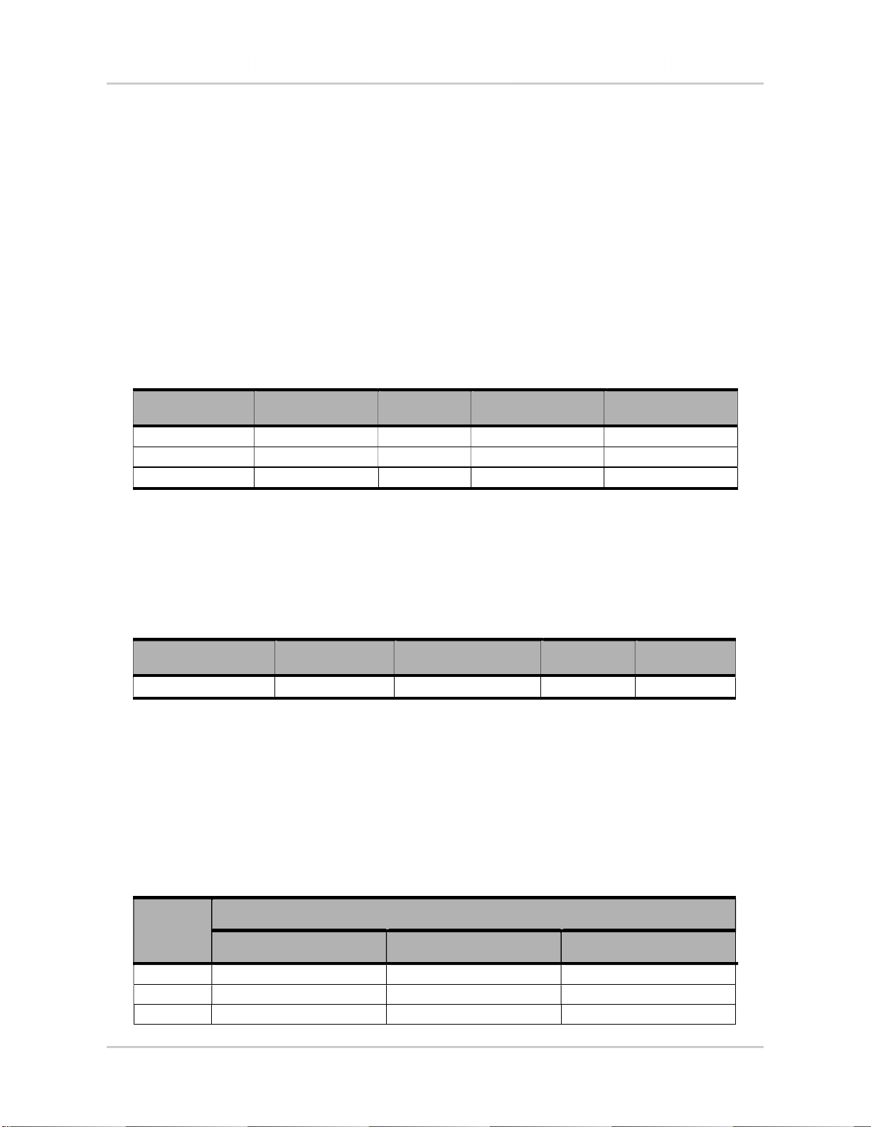
Product Technical Specification Detailed Interface Specifications
3.19. RF Interface
The RF interface of the AirPrime HL7800 and HL7800-M modules allow the transmission of RF
signals.
Contact Sierra Wireless technical support for assistance in integrating the AirPrime HL7800 or
HL7800-M on applications with embedded antennas.
3.19.1. RF Connection
A 50Ω (with maximum VSWR 1.1:1, and 0.5dB loss) RF track is recommended to be connected to
standard RF connectors such as SMA, UFL, etc. for antenna connection.
Refer to the following table for the pad description of the RF interface.
Table 38. RF Main Pin Description
Pad Number RF Signal Impedance VSWR Rx (m ax) VSWR Tx (max)
C48 GND
C49 RF_MAIN 50Ω 2.5:1 2.5:1
C50 GND
3.19.2. Maximum Output Power
The maximum transmitter output power of the AirPrime HL7800 and HL7800-M for all bands in normal
operation conditions (25°C) is specified in the following table.
Table 39. Maximum Output Power
Minimum Typical Maximum Units Notes
21.5 23 24.5 dBm Power class 3
3.19.3. Rx Sensitivity
The module’s receiver sensitivity is specified in the following table. The test condition used for the
following values are as follows:
Cat-M1
BW: 5 MHz
Table 40. Typical Conducted RX Sensitivity
Typical Referen ce Sen sitivity Level @ 95% of the Maximum Throughput
LTE Band
@+25°C (dBm) @Cl ass A (dBm) 3GPP Limit (dBm)
B1 -105 (TBC) TBD -102.3
B2 -106 (TBC) TBD -100.3
B3 -106.5 -102.8 -99.3
41111094 Rev 1.7 August 10, 2018 42
Page 43

Product Technical Specification Detailed Interface Specifications
Typical Referen ce Sen sitivity Level @ 95% of the Maximum Throughput
LTE Band
@+25°C (dBm) @Cl ass A (dBm) 3GPP Limit (dBm)
B4 -105.7 -103.7 (TBC) -102.3
B5 -106.5 -104.5 -100.8
B8 -106.8 (TBC) TBD -99.8
B9 -106 TBD TBD
B10 -105 (TBC) TBD TBD
B12 -105.7 -105.1 -99.3
B13 -106 -104.9 -99.3
B14 -106 -105 TBD
B17 -106 -104.8 TBD
B18 -106.5 -105 -100.3
B19 -106.3 -105.5 -102.3
B20 -106 -104 -99.8
B25 -105.7 (TBC) TBD TBD
B26 -107 -104.8 -100.3
B27 -106.7 -105 -100.8
B28 -106.2 (TBC) TBD -100.8
B66 -105.5 (TBC) TBD TBD
3.19.4. TX Indicator (TX_ON)
The AirPrime HL7800 and HL7800-M modules provide a signal, TX_ON, for TX emission indication.
Table 41. TX_ON Pin Description
Pad Number Signal Name I/O I/ O Typ e Description
C60 TX_ON 0 1.8V High during TX emission, low when there is no TX
TX_ON
VBATT_PA
T
advance
Figure 12. TX_ON State during TX Burst
T
duration
Voltage drop
T
delay
41111094 Rev 1.7 August 10, 2018 43
Page 44

Product Technical Specification Detailed Interface Specifications
Table 42. TX_ON Characteristics
Parameter Typical
Tadvance 30 µs
Tdelay TBD
3.20. GPS Interface
Note: This interface will be available in a future release.
The AirPrime HL7800 and HL7800-M’s GPS supports GPS L1 signal (1575.42 ± 20 MHz) and
GLONASS L1 FDMA signals (1597.5 – 1605.8 MHz), with 50Ω connection on the RF_GPS pad.
Note: The GPS receiver shares the same RF resources as the 4G receiver. The end-device target should
allow GPS positioning for asset management applications where infrequent and no real-time
position updates are required.
GPS antenna interface specifications are defined in the table below.
Table 43. GPS Antenna Specifications
Characteristics Valu e
Frequency (MHz) GPS L1 1575.42 ± 20
RF Impedance (Ω) 50
VSWR max 2:1
3.20.1. GPS Performance
Refer to the following table for GPS performance details.
Table 44. GPS Performance
Parameters Conditions Typical Val ue
Cold Start -146dBm (TBC)
Sensitivity
TTFF
2D Position Error Input power -130dBm 2.5m (TBC)
Hot Start -152dBm (TBC)
Tracking -161dBm (TBC)
Cold start, Input power -130dBm 35s (TBC)
Hot start, Input power -130dBm 2s (TBC)
3.20.2. GPS Antenna Indicator (EXT_LNA_GPS_EN)
Note: This signal will be available in a future release.
41111094 Rev 1.7 August 10, 2018 44
Page 45

4. Mechanical Drawings
Figure 13. Mechanical Drawing
41111094 Rev 1.7 August 10, 2018 45
Page 46

Product Technical Specification Mechanical Drawings
Figure 14. Dimensions Drawing
41111094 Rev 1.7 August 10, 2018 46
Page 47

Product Technical Specification Mechanical Drawings
Figure 15. Footprint Drawing
41111094 Rev 1.7 August 10, 2018 47
Page 48

5. Reliability Specification
The AirPrime HL7800 and HL7800-M modules will be tested against the Sierra Wireless Industrial
Reliability Specification defined below.
5.1. Preconditioning Test
Per JESD22A113, this test the preconditioning of non-hermetic surface mount devices prior to
reliability testing.
Table 45. Preconditioning Test
Designation Condition
Preconditioning Test
PCRM
2 reflow cycles with Tmax 245-250°C
5.2. Performance Test
Table 46. Performance Test
Designation Condition
Performance Test
PT3T & PTRT
Standard: N/A
Special conditions:
Temperature:
Class A: -30°C to +70°C
Class B: -40°C to +85°C
Rate of temperature change: ± 3°C/min
Recovery time: 3 hours
Operating conditions: Powered
Duration: 14 days
41111094 Rev 1.7 August 10, 2018 48
Page 49

Product Technical Specification Reliability Specification
5.3. Aging Tests
Table 47. Aging Tests
Designation Condition
High Temperature Operating
Life test
HTOL
Thermal Shock Test
TSKT
Humidity Test
HUT
Standard: IEC 680068-2-2, Test Bb
Special conditions:
Temperature: +85°C
Temperature variation: 1°C/min
Operating conditions: Powered ON with a power cycle of 45 minutes ON
and 15 minutes Idle
Duration: 20 days
Standard: IEC 60068-2-14, Test Na
Special conditions:
Temperature: -40°C to +85°C
Temperature Variation: less than 30s
Number of cycles: 300
Dwell Time: 10 minutes
Operating conditions: Un-powered
Duration: 7 days
Standard: IEC 60068-2-3, Test Ca
Special conditions:
Temperature: +85°C
RH: 85%
Operating conditions: Powered on, DUT is powered up for 15 minutes and
OFF for 15 minutes
Duration: 10 days
41111094 Rev 1.7 August 10, 2018 49
Page 50

Product Technical Specification Reliability Specification
5.4. Characterization Tests
Table 48. Characterization Tests
Designation Condition
Special conditions:
Low Temperature and Cold
Start Cycles
LTCS
Component Solder Wettability
CSW
Unprotected Free Fall Test
FFT 1
Temperature: -40°C
AT commands read or write memory
Operating conditions: 5 mins powered ON, 30 mins powered OFF (1
power cycle)
Duration: 5 days
Standard: JESD22 – B102, Method 1/Condition C, Solderability Test
Method
Special conditions:
Test method: Surface mount process simulation test
(preconditioning 16 h ±30 minutes dry bake)
Operating conditions: Un-powered
Duration: 1 day
Standard: IEC 60068-2-32, Test Ed
Special conditions:
Number of drops: 6 drops per unit (1 drop per direction: ±X, ±Y,
±Z)
Height: 1m
Operating conditions: Un-powered
Duration: 1 day
41111094 Rev 1.7 August 10, 2018 50
Page 51

6. Legal Information
6.1. Japan Radio and Telecom Approval
The end device embedding the AirPrime HL7800 or HL7800-M should affix the certification indication
on its surface following the recommendations below:
The diameter of the Japan Approval mark must be 3mm or bigger.
The size, font and color of the Radio Certification Type number is not regulated but should be
easily distinguished.
Figure 16. Sample Japan Certification Indication
6.2. FCC Statement
6.2.1. Applicable Rules
Here is a list of the FCC rules applicable to the product:
- FCC Part 2
- FCC Part 22, Subpart H
- FCC Part 24, Subpart E
- FCC Part 27, Subpart C, H, F, L
- FCC Part 90, Subpart I, S, R
6.2.2. Radiation Exposure Statement
This equipment has been granted modular approval for mobile applications. Integrators may use this
equipment in their end products without additional FCC certification if they meet the following
conditions. Otherwise, additional FCC approvals must be obtained.
1. The end product must use the RF trace design approved with the equipment. The Gerber file
of the trace design can be obtained from Sierra Wireless upon request.
2. At least 20 cm separation distance between the antenna and the user’s body must be
maintained at all times.
3. To comply with FCC/IC regulations limiting both maximum RF output power and human
exposure to RF radiation, the maximum antenna gain including cable loss in a mobile-only
exposure condition must not exceed the limits stipulated in the below table
41111094 Rev 1.7 August 10, 2018 51
Page 52

Product Technical Specification Legal Information
Operating Band
LTE Band 2 1850 1910 6 6
LTE Band 4 1710 1755 6 6
LTE Band 5 824 849 6 4
LTE Band 12 699 716 6 4
LTE Band 13 777 787 6 4
LTE Band 14 788 798 6 3
LTE Band 17 704 716 6 3
LTE Band 25 1850 1915 6 6
LTE Band 26 814 849 6 3
LTE Band 66 1710 1780 6 6
4. The equipment may transmit simultaneously with other collocated radio transmitters within a
host device, provided the following conditions are met:
a. Each collocated radio transmitter has been certified by FCC/IC for mobile application.
b. At least 20 cm separation distance between the antennas of the collocated
transmitters and the user’s body must be maintained at all times.
c. The radiated power of a collocated transmitter must not exceed the EIRP limit
stipulated in the table below.
TX Freq Range
(MHz)
Antenna Gain Limits(dBi)
Standalone Collocated
Operating Mode TX Freq Range (MHz) EIRP Limits (dBm)
WLAN 2.4 GHz 2400 - 2500 30
WLAN 5 GHz 5150 - 5850 30
BT 2400 - 2500 16
WiGig 58320 - 62640 25
The end product with this equipment embedded may also need to pass the FCC Part 15 unintentional
emission testing requirements and be properly authorized per FCC Part 15.
6.2.3. End Product Labeling
6.2.3.1. HL7800-M
41111094 Rev 1.7 August 10, 2018 52
Page 53

Product Technical Specification Legal Information
This transmitter module is authorized only for use in device where the antenna may be installed such
that 20 cm may be maintained between the antenna and users. The final end product must be labeled
in a visible area with the following: “Contains FCC ID: N7NHL78M”. The grantee's FCC ID can be
used only when all FCC compliance requirements are met.
6.2.3.1. HL7800
This transmitter module is authorized only for use in device where the antenna may be installed such
that 20 cm may be maintained between the antenna and users. The final end product must be labeled
in a visible area with the following: “Contains FCC ID: N7NHL78”. The grantee's FCC ID can be used
only when all FCC compliance requirements are met.
6.2.4. Manual Information to the End User
The OEM integrator has to be aware not to provide information to the end user regarding how to
install or remove this RF module in the user’s manual of the end product which integrates this module.
The end user manual shall include all required regulatory information/warning as show in this manual.
Antenna installation:
The RF signal must be routed on the application board using tracks with a 50Ω characteristic
impedance. Basically, the characteristic impedance depends on the dielectric, the track width and the
ground plane spacing. In order to respect this constraint, Sierra Wireless recommends using
MicroStrip or StripLine structure and computing the Tracks width with a simulation tool (like AppCad
shown in the figure below and that is available free of charge at http://www.agilent.com).
If a multi-layered PCB is used, the RF path on the board must not cross any signal (digital, analog or
supply).
If necessary, use StripLine structure and route the digital line(s) "outside" the RF structure. An
example of proper routing is shown in the figure below.
41111094 Rev 1.7 August 10, 2018 53
Page 54

Product Technical Specification Legal Information
Stripline and Coplanar design requires having a correct ground plane at both sides. Consequently, it
is necessary to add some vias along the RF path. It is recommended to use Stripline design if the RF
path is fairly long (more than 3cm), since MicroStrip design is not shielded. Consequently, the RF
signal (when transmitting) may interfere with neighbouring electronics (AF amplifier, etc.). In the same
way, the neighbouring electronics (microcontrollers, etc.) may degrade the reception performances.
The GSM/GPRS connector is
intended to be directly connected to a 50Ω antenna and no matching is needed.
6.3. IC Statement
This device complies with Industry Canada license-exempt RSS standard(s). Operation is subject to
the following two conditions:
1. this device may not cause interference, and
2. this device must accept any interference, including interference that may cause undesired
operation of the device.
Le présent appareil est conforme aux CNR d'Industrie Canada applicables aux appareils radio
exempts de licence. L'exploitation est autorisée aux deux conditions suivantes:
1. l'appareil ne doit pas produire de brouillage, et
2. l'utilisateur de l'appareil doit accepter tout brouillage radioélectrique subi, même si le
brouillage est susceptible d'en compromettre le fonctionnement.
This Class B digital apparatus complies with Canadian ICES-003.
Cet appareil numérique de la classe B est conforme à la norme NMB-003 du Canada.
This device complies with RSS-310 of Industry Canada. Operation is subject to the condition that this
device does not cause harmful interference.
Cet appareil est conforme à la norme RSS-310 d'Industrie Canada. L'opération est soumise à la
condition que cet appareil ne provoque aucune interférence nuisible.
This device and its antenna(s) must not be co-located or operating in conjunction with any other
antenna or transmitter, except tested built-in radios.
Cet appareil et son antenne ne doivent pas être situés ou fonctionner en conjonction avec une autre
antenne ou un autre émetteur, exception faites des radios intégrées qui ont été testées.
41111094 Rev 1.7 August 10, 2018 54
Page 55

Product Technical Specification Legal Information
The County Code Selection feature is disabled for products marketed in the US/ Canada.
La fonction de sélection de l'indicatif du pays est désactivée pour les produits commercialisés aux
États-Unis et au Canada.
6.3.1. Radiation Exposure Statement / Déclaration
d'Exposition aux Radiations
This equipment complies with IC radiation exposure limits set forth for an uncontrolled environment.
This equipment should be installed and operated with minimum distance 20 cm between the radiator
and your body.
Cet équipement est conforme aux limites d'exposition aux rayonnements IC établies pour un
environnement non contrôlé. Cet équipement doit être installé et utilisé avec un minimum de 20 cm de
distance entre la source de rayonnement et votre corps.
This device is intended only for OEM integrators under the following conditions: (For module device
use)
1. The antenna must be installed such that 20 cm is maintained between the antenna and users,
and
2. The transmitter module may not be co-located with any other transmitter or antenna.
As long as the 2 conditions above are met, further transmitter test will not be required. However, the
OEM integrator is still responsible for testing their end-product for any additional compliance
requirements required with this module installed.
Cet appareil est conçu nt pour les intégrateurs OEM dans les conditions suivantes: (Pour utilisation de
dispositif module)
1. L'antenne doit être installée de telle sorte qu'une distance de 20 cm est respectée entre
l'antenne et les utilisateurs, et
2. Le module émetteur peut ne pas être coïmplanté avec un autre émetteur ou antenne.
Tant que les 2 conditions ci-dessus sont remplies, des essais supplémentaires sur l'émetteur ne
seront pas nécessaires. Toutefois, l'intégrateur OEM est toujours responsable des essais sur son
produit final pour toutes exigences de conformité supplémentaires requis pour ce module installé.
IMPORTANT NOTE:
configurations or co-location with another transmitter), then the Canada authorization is no longer
considered valid and the IC ID cannot be used on the final product. In these circumstances, the OEM
integrator will be responsible for re-evaluating the end product (including the transmitter) and
obtaining a separate Canada authorization.
NOTE IMPORTANTE:
certaines configurations d'ordinateur portable ou de certaines co-localisation avec un autre émetteur),
l'autorisation du Canada n'est plus considéré comme valide et l'ID IC ne peut pas être utilisé sur le
produit final. Dans ces circonstances, l'intégrateur OEM sera chargé de réévaluer le produit final (y
compris l'émetteur) et l'obtention d'une autorisation distincte au Canada.
41111094 Rev 1.7 August 10, 2018 55
In the event that these conditions cannot be met (for example certain laptop
Dans le cas où ces conditions ne peuvent être satisfaites (par exemple pour
Page 56

Product Technical Specification Legal Information
6.3.2. End Product Labeling / Plaque Signalétique du
Produit Final
6.3.2.1. HL7800-M
This transmitter module is authorized only for use in device where the antenna may be installed such
that 20 cm may be maintained between the antenna and users. The final end product must be labeled
in a visible area with the following: “Contains IC: 2417C-HL78M”.
Ce module émetteur est autorisé uniquement pour une utilisation dans un dispositif où l'antenne peut
être installée de telle sorte qu'une distance de 20cm peut être maintenue entre l'antenne et les
utilisateurs. Le produit final doit être étiqueté dans un endroit visible avec l'inscription suivante:
"Contient des IC: 2417C-HL78M".
6.3.2.1. HL7800
This transmitter module is authorized only for use in device where the antenna may be installed such
that 20 cm may be maintained between the antenna and users. The final end product must be labeled
in a visible area with the following: “Contains IC: 2417C-HL78”.
Ce module émetteur est autorisé uniquement pour une utilisation dans un dispositif où l'antenne peut
être installée de telle sorte qu'une distance de 20cm peut être maintenue entre l'antenne et les
utilisateurs. Le produit final doit être étiqueté dans un endroit visible avec l'inscription suivante:
"Contient des IC: 2417C-HL78".
6.3.3. Manual Information to the End User / Manuel
d'Information à l'Utilisateur Final
The OEM integrator has to be aware not to provide information to the end user regarding how to
install or remove this RF module in the user’s manual of the end product which integrates this module.
The end user manual shall include all required regulatory information/warning as show in this manual.
L'intégrateur OEM doit être conscient de ne pas fournir des informations à l'utilisateur final quant à la
façon d'installer ou de supprimer ce module RF dans le manuel de l'utilisateur du produit final qui
intègre ce module.
Le manuel de l'utilisateur final doit inclure toutes les informations réglementaires requises et
avertissements comme indiqué dans ce manuel.
41111094 Rev 1.7 August 10, 2018 56
Page 57

7. Ordering Information
Table 49. Ordering Information
Model N ame Description Part Numb er
HL7800 HL7800 embedded module Contact Sierra Wireless for the latest SKU
HL7800-M HL7800-M embedded module Contact Sierra Wireless for the latest SKU
DEV-KIT HL Series Development Kit TBD
41111094 Rev 1.7 August 10, 2018 57
Page 58

8. Terms and Abbreviations
Abbr eviation Definition
ADC Analog to Digital Converter
AGC Automatic Gain Control
AT Attention (prefix for modem commands)
CDMA Code Division Multiple Access
CF3 Common Flexible Form Factor
CLK Clock
CODEC Coder Decoder
CPU Central Processing Unit
DAC Digital to Analog Converter
DTR Data Terminal Ready
DRX Discontinuous Reception
eDRX Extended DRX
EMC Electro-Magnetic Compatibility
EMI Electro-Magnetic Interference
EN Enable
ESD Electro-Static Discharges
ETSI European Telecommunications Standards Institute
FDMA Frequency-division multiple access
GLONASS Global Navigation Satellite System
GND Ground
GNSS Global Navigation Satellite System
GPIO General Purpose Input Output
GPRS General Packet Radio Service
GSM Global System for Mobile communications
Hi Z High impedance (Z)
IC Integrated Circuit
IMEI International Mobile Equipment Identification
I/O Input / Output
LED Light Emitting Diode
LNA Low Noise Amplifier
MAX Maximum
MIN Minimum
N/A Not Applicable
PA Power Amplifier
PC Personal Computer
PCB Printed Circuit Board
PCL Power Control Level
PLL Phase Lock Loop
PSM Power Save Mode
PSRAM Pseudo Static RAM
PSU Power Supply Unit
41111094 Rev 1.7 August 10, 2018 58
Page 59

Product Technical Specification Terms and Abbreviations
Abbr eviat ion Definition
PTW Paging Time Window
PWM Pulse Width Modulation
RF Radio Frequency
RFI Radio Frequency Interference
RMS Root Mean Square
RST Reset
RTC Real Time Clock
RX Receive
SCL Serial Clock
SDA Serial Data
SIM Subscriber Identification Module
SMD Surface Mounted Device/Design
SPI Serial Peripheral Interface
SW Software
TBC To Be Confirmed
TBD To Be Defined
TP Test Point
TX Transmit
TYP Typical
UART Universal Asynchronous Receiver-Transmitter
UICC Universal Integrated Circuit Card
USB Universal Serial Bus
UIM User Identity Module
VBATT Main Supply Voltage from Battery or DC adapter
VSWR Voltage Standing Wave Ratio
41111094 Rev 1.7 August 10, 2018 59
 Loading...