


Siemens MGP3006X Datasheet
GHz PLL with I2C Bus
and Four Chip Addresses
Features
● 1-chip system for MPU-control (I
● 4 programmable chip addresses
● Short pull-in time for quick channel switch-over
and optimized loop stability
● 2 high-current band switch outputs (20 mA)
● Software-compatible with SDA 3202 series
● Oxis III technology
Type Ordering Code Package
2
C Bus)
P-DSO-14-1
MGP 3006X
Bipolar IC
MGP 3006X Q67000-H5114 P-DSO-14-1 (SMD)
MGP 3006X Q67006-H5114 P-DSO-14-1 Tape & Reel (SMD)
Combined with a VCO (tuner), the MGP 3006X device, with four hard-switched chip
addresses, forms a digitally programmable phase-locked loop for use in television sets
with PLL-frequency synthesis tuning. The PLL permits precise crystal-controlled setting
of the frequency of the tuner oscillator between 16 and 1300 MHz in increments of
62.5 kHz, and, with a 2.4-GHz prescaler 1/2, in the TV-SAT band in increments of
125 kHz. The tuning process is controlled by a microprocessor via an I
2
I
C Bus noise immunity has been improved by a factor of 10 compared to the
2
C Bus. The
SDA 3202-2, and the new crystal oscillator generates a sinusoidal signal, suppressing
the higher-order harmonics, which reduces the moiré noise considerably.
Semiconductor Group 1 04.93

MGP 3006X
Circuit Description
Tuning Section
UHF/VHF The tuner signal is capacitively coupled at the UHF/VHF-input and
subsequently amplified.
REF The reference input REF should be decoupled to ground using a capacitor
of low series inductance. The signal passes through an asynchronous
divider with a fixed ratio of
through 32767, and is then compared in a digital frequency/phase
detector to a reference frequency
Q1, Q2 This frequency is derived from a balanced, low-impedance 4-MHz crystal
oscillator (pin Q1, Q2) by dividing its output signal by
The phase detector has two outputs UP and DOWN that drive the two
current sources I+ and I– of a charge pump. If the negative edge of the
divided VCO-signal appears prior to the negative edge of the reference
signal, the I+ current source pulses for the duration of the phase
difference. In the reverse case the I– current source pulses.
P = 8, an adjustable divider with ratio N = 256
f
= 7.8125 kHz.
REF
Q = 512.
PD, UD If the two signals are in phase, the charge pump output (PD) goes into the
high-impedance state (PLL is locked). An active low-pass filter integrates
the current pulses to generate the tuning voltage for the VCO (internal
amplifier, external output transistor at UD and external RC-circuitry). The
charge pump output is also switched into the high-impedance state when
the control bit T0 = 1. Here it should be noted, however, that the tuning
voltage can alter over a long period in the high-impedance state as a
result of self-discharge in the peripheral circuitry. UD may be switched off
by the control bit OS to allow external adjustments.
By means of a control bit 5I the pump current can be switched between
two values by software. This programmability permits alteration of the
control response of the PLL in the locked-in state. In this way different
VCO-gains in the different TV-bands can be compensated, for example.
P1, P2 The software-switched outputs P1, P2 can be used for direct band
selection (20 mA current output).
P7 P7 is a general-purpose open-collector output. The test bit T1 = 1
switches the test signal Cy (divided input signal) to P7.
CAU Four different chip addresses can be set by appropriate connection of pin
CAU.
Semiconductor Group 2

MGP 3006X
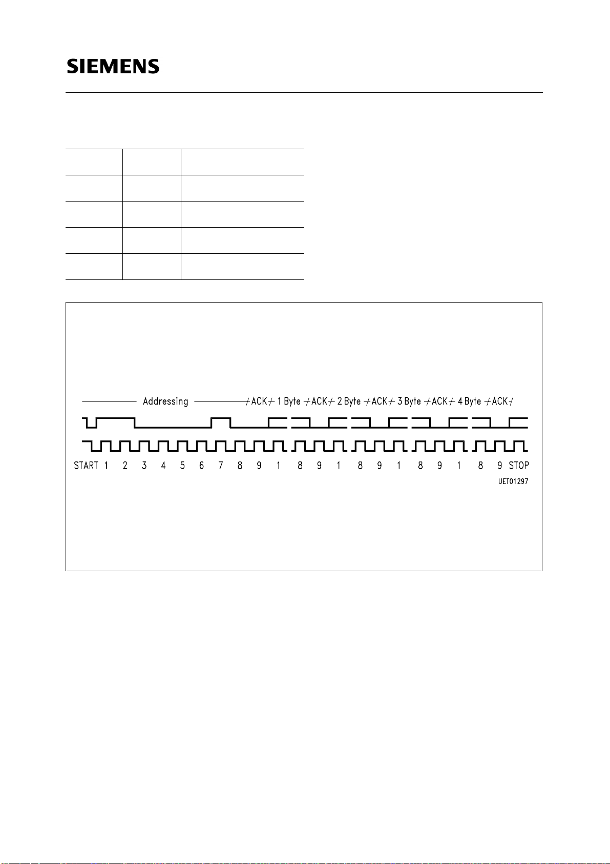
I2C Bus Interface
2
Data are exchanged between the processor and the PLL on the I
SCL, SDA The clock is generated by the processor (input SCL), while pin SDA works
as an input or output depending on the direction of the data (open
collector; external pull-up resistor). Both inputs have hysteresis and a
low-pass characteristic, which enhances the noise immunity of the I
Bus.
2
The data from the processor pass through an I
C Bus control. Depending
on their function the data are subsequently stored in registers. If the bus
is free, both lines will be in the marking state (SDA, SCL are high). Each
telegram begins with the start condition and ends with the stop condition.
Start condition: SDA goes low, while SCL remains high. Stop condition:
SDA goes high while SCL remains high. All further information transfer
takes place during SCL = low, and the data is forwarded to the control
logic on the positive clock edge.
C Bus.
2
C
The table “bit allocation” should be referred to in the following paragraph.
All telegrams are transmitted byte-by-byte, followed by a ninth clock
pulse, during which the control logic returns the SDA-line to low
(acknowledge condition). The first byte is comprised of seven address
bits. These are used by the processor to select the PLL from several
peripheral components (chip select). The eighth bit is always low.
In the data portion of the telegram the first bit of the first or third data byte
determines whether a divider ratio or control information is to follow. In
each case the second byte of the same data type or a stop condition has
to follow the first byte.
V
, GND When the supply voltage is applied a power-on reset circuit prevents the
S
PLL from setting the SDA-line to low, which would block the bus.
Semiconductor Group 3
MGP 3006X
Circuit Description (cont’d)
Bit Allocation
MSB A = Acknowledge
Address byte 1 1 0 0 0 MA1 MA0 0 A
Prog. divider Byte 1 0 n14 n13 n12 n11 n10 n9 n8 A
Prog. divider Byte 2 n7 n6 n5 n4 n3 n2 n1 n0 A
Control info. Byte 1 1 5I T1 T0 1 1 1 OS A
Control info. Byte 2 P7 X X X X P2 P1 X A
Divider Ratio
N = 16384 × n14 + 8192 × n13 + 4096 × n12 + 2048 × n11 + 1024 × n10 + 512 × n9 +
256 × n8 + 128 × n7 + 64 × n6 + 32 × n5 + 16 × n4 + 8 × n3 + 4 × n2 + 2 × n1 + n0
Band Selection
P1, P2, P7 = 1 Open-collector output is active.
Pump Current Programming
5I = 1 High current
UD Disable
OS = 1 UD is disabled.
Test Mode
T1, T0 = 0, 0 Normal operation
T1 = 1 P7 = carry Cy of programmable divider
T0 = 1 Tristate: charge pump output PD is in high-impedance state.
Semiconductor Group 4
Chip Address Switching
MA1 MA0 Voltage at CAU
MGP 3006X
0 0 (0 … 0.1)
V
0 1 open-circuit
1 0 (0.4 … 0.6)
1 1 (0.9 … 1) V
S
V
S
S
Telegram Examples
Start-Addr-DR1-DR2-CW1-CW2-Stop Start = start condition
Start-Addr-CW1-CW2-DR1-DR2-Stop Addr = address
Start-Addr-DR1-DR2-CW1-Stop DR1 = divider ratio 1st byte
Start-Addr-CW1-CW2-DR1-Stop DR2 = divider ratio 2nd byte
Start-Addr-DR1-DR2-Stop CW1 = control word 1st Byte
Start-Addr-CW1-CW2-Stop CW2 = control word 2nd Byte
Start-Addr-DR1-Stop Stop = stop condition
Start-Addr-CW1-Stop
Semiconductor Group 5
Pin Configuration
(top view)
MGP 3006X
Semiconductor Group 6
Pin Definitions and Functions
Pin No. Symbol Function
1 PD Input active filter/charge pump output
2 Q1 Quartz crystal
3 Q2 Quartz crystal
MGP 3006X
C Bus
2
C Bus
4 SDA Data input/output for I
5 SCL Clock input for I
2
6 P7 Port output (open collector)
7 CAU Address switch input
8 P2 Port output (open collector)
9 P1 Port output (open collector)
10
V
S
Supply voltage
11 UHF/VHF Signal input
12 REF Amplifier reference input
13 GND Ground
14 UD Output active filter
Semiconductor Group 7