

Page 1
SENTRON 3WL / 3VL
Library for SIMATIC PCS 7 V1.0
Function Manual
•
11/2008
SIMATIC
Page 2

Page 3

Library SENTRON 3WL / 3VL for
SIMATIC PCS 7
Function Manual
Introduction
Information about the library
Description of blocks
Configuration Manual
Technical specifications
Technical support
1
2
3
4
5
6
V1.0
11/2008
A5E02316914A-01
Page 4
Legal information
Warning notice system
This manual contains notices you have to observe in order to ensure your personal safety, as well as to prevent
damage to property. The notices referring to your personal safety are highlighted in the manual by a safety alert
symbol, notices referring only to property damage have no safety alert symbol. These notices shown below are
graded according to the degree of danger.
DANGER
indicates that death or severe personal injury will result if proper precautions are not taken.
WARNING
indicates that death or severe personal injury may result if proper precautions are not taken.
CAUTION
with a safety alert symbol, indicates that minor personal injury can result if proper precautions are not taken.
CAUTION
without a safety alert symbol, indicates that property damage can result if proper precautions are not taken.
NOTICE
indicates that an unintended result or situation can occur if the corresponding information is not taken into
account.
If more than one degree of danger is present, the warning notice representing the highest degree of danger will
be used. A notice warning of injury to persons with a safety alert symbol may also include a warning relating to
property damage.
Qualified Personnel
The device/system may only be set up and used in conjunction with this documentation. Commissioning and
operation of a device/system may only be performed by qualified personnel. Within the context of the safety notes
in this documentation qualified persons are defined as persons who are authorized to commission, ground and
label devices, systems and circuits in accordance with established safety practices and standards.
Proper use of Siemens products
Note the following:
WARNING
Siemens products may only be used for the applications described in the catalog and in the relevant technical
documentation. If products and components from other manufacturers are used, these must be recommended
or approved by Siemens. Proper transport, storage, installation, assembly, commissioning, operation and
maintenance are required to ensure that the products operate safely and without any problems. The permissible
ambient conditions must be adhered to. The information in the relevant documentation must be observed.
Trademarks
All names identified by ® are registered trademarks of the Siemens AG. The remaining trademarks in this
publication may be trademarks whose use by third parties for their own purposes could violate the rights of the
owner.
Disclaimer of Liability
We have reviewed the contents of this publication to ensure consistency with the hardware and software
described. Since variance cannot be precluded entirely, we cannot guarantee full consistency. However, the
information in this publication is reviewed regularly and any necessary corrections are included in subsequent
editions.
Siemens AG
Industry Sector
Postfach 48 48
90026 NÜRNBERG
GERMANY
A5E02316914A-01
Ⓟ 11/2008
Copyright © Siemens AG 2008.
Technical data subject to change
Page 5

Table of contents
1 Introduction................................................................................................................................................ 7
1.1 General ..........................................................................................................................................7
1.2 Further documentation
1.3 Installing the library
1.4 Hardware configuration
1.4.1 Incorporating v
2 Information about
2.1 Overview of the blocks.................................................................................................................13
2.2 General information about OS ty
2.2.1 Faceplates....................................................................................................................................13
2.2.2 Symbols .......................................................................................................................................15
3 Description of
3.1 Diagnostics block DIA_WLVL ......................................................................................................17
3.1.1 Calling OBs
3.1.2 Called blocks................................................................................................................................18
3.1.3 Function .......................................................................................................................................18
3.1.4 Message behavior........................................................................................................................18
3.1.5 Error behavior ..............................................................................................................................19
3.1.6 I/O access error ...........................................................................................................................19
3.1.7 Module fault..................................................................................................................................19
3.1.8 Read diagnostics data of 3WL / 3VL
3.1.9 Start-up characteristics ................................................................................................................20
3.1.10 Block parameters .........................................................................................................................20
3.2 Driver module DRV
3.2.1 Calling OBs
3.2.2 Called blocks................................................................................................................................23
3.2.3 Function .......................................................................................................................................23
3.2.4 Message behavior........................................................................................................................26
3.2.5 Assignment of the cycli
3.2.6 Addressing and modul
3.2.7 Processing the diagnostics data of the 3WL dev
3.2.8 Start-up characteristics ................................................................................................................29
3.2.9 Block parameters .........................................................................................................................29
3.2.10 Description of symbols and faceplates ........................................................................................60
the library .................................................................................................................... 13
blocks................................................................................................................................ 17
ia GSD file..............................................................................................................8
..................................................................................................................................18
..................................................................................................................................22
...................................................................................................................7
........................................................................................................................7
..................................................................................................................8
picals ........................................................................................13
...........................................................................................19
_3WL.............................................................................................................22
c process image......................................................................................27
e driver .....................................................................................................28
ice ....................................................................28
3.3 Driver module DRV
3.3.1 Calling OBs
3.3.2 Called blocks................................................................................................................................96
3.3.3 Function .......................................................................................................................................96
3.3.4 Message behavior........................................................................................................................99
3.3.5 Assignment of the cycli
3.3.6 Addressing and modul
3.3.7 Processing the diagnostics data of the 3VL device ...................................................................102
3.3.8 Start-up characteristics ..............................................................................................................102
Library SENTRON 3WL / 3VL for SIMATIC PCS 7
Function Manual, 11/2008, A5E02316914A-01
..................................................................................................................................96
_3VL..............................................................................................................95
c process image....................................................................................100
e driver ...................................................................................................101
3
Page 6

Table of contents
3.3.9 Block parameters ...................................................................................................................... 102
3.3.10 Description of symbols and faceplates ..................................................................................... 111
4 Configuration
4.1 Interconnections on COM15 for 3WL
4.1.1 24V DC voltage ......................................................................................................................... 126
4.1.2 Other voltage lev
4.2 Interconnections on COM10 for 3VL
4.2.1 Connection for c
4.2.2 Connection for motorized operating mechanism
4.3 Connection on COM20 for
4.3.1 COM20 pin assignment............................................................................................................. 130
4.3.2 Connecting the optional motorized op
4.4 Configuring a meas
4.4.1 Creating the PLC program
4.4.2 Connection to WinCC................................................................................................................ 135
5 Technical specif
6 Technical su
Figures
Figure 1-1
Figure 1-2 Selection of basic type for 3WL .................................................................................................... 8
Figure 1-3 Selection of basic type for 3VL ..................................................................................................... 9
Catalog path for incorporating via GSD file................................................................................... 8
Manual............................................................................................................................. 125
........................................................................................ 125
els .................................................................................................................. 127
......................................................................................... 128
ommunication ................................................................................................. 128
...................................................................... 129
3VL................................................................................................. 130
erating mechanism to COM20 ...................................... 131
uring point .................................................................................................. 132
........................................................................................................ 132
ications......................................................................................................................... 139
pport .................................................................................................................................. 141
Figure 1-4 Properties of the 3WL / 3VL device directly connected to the DP master system...................... 10
Figure 1-5 Properties of the 3WL / 3VL device following a Y link ................................................................ 11
Figure 2-1 Section of the overview display................................................................................................... 13
Figure 2-2 Trend setting on the icon............................................................................................................. 14
Figure 2-3 Icons in Graphics Designer......................................................................................................... 15
Figure 3-1 Symbol with 1 measurement....................................................................................................... 61
Figure 3-2 Faceplate for standard view........................................................................................................ 63
Figure 3-3 Faceplate for measurements view, current tab........................................................................... 65
Figure 3-4 Faceplate for measurements view, voltage tab .......................................................................... 66
Figure 3-5 Faceplate for measurements view, active power/energy tab...................................................... 67
Figure 3-6 Faceplate for measurements view, reactive power/energy tab .................................................. 68
Figure 3-7 Faceplate for measurements view, apparent power tab............................................................. 69
Figure 3-8 Faceplate for measurements view, miscellaneous tab............................................................... 70
Figure 3-9 Faceplate for diagnosis view, warnings tab ................................................................................ 71
Figure 3-10 Faceplate for diagnosis view, trip reason tab.............................................................................. 72
Figure 3-11 Faceplate for diagnosis view, setpoints tab ................................................................................ 74
Figure 3-12 Faceplate for maintenance view, maintenance 1 tab ................................................................. 76
Library SENTRON 3WL / 3VL for SIMATIC PCS 7
4 Function Manual, 11/2008, A5E02316914A-01
Page 7

Table of contents
Figure 3-13 Faceplate for maintenance view, maintenance 2 tab ..................................................................77
Figure 3-14 Faceplate for maintenance view, operation tab...........................................................................79
Figure 3-15 Faceplate for protect. para view, parameter set A.......................................................................80
Figure 3-16 Faceplate for protect. para view, parameter set B.......................................................................82
Figure 3-17 Faceplate for protect. para view, additional tab...........................................................................84
Figure 3-18 Faceplate for ext. protect. para view, current tab ........................................................................85
Figure 3-19 Faceplate for ext. protect. para view, voltage tab........................................................................86
Figure 3-20 Faceplate for ext. protect. para view, reactive power tab ............................................................87
Figure 3-21 Faceplate for ext. protect. para view, frequency tab....................................................................88
Figure 3-22 Faceplate for setpoints view, current tab .....................................................................................89
Figure 3-23 Faceplate for setpoints view, voltage tab.....................................................................................90
Figure 3-24 Faceplate for setpoints view, frequency tab ................................................................................91
Figure 3-25 Faceplate for setpoints view, active power tab............................................................................92
Figure 3-26 Faceplate for setpoints view, apparent/reactive power tab .........................................................94
Figure 3-27 Faceplate for message suppression view....................................................................................95
Figure 3-28 Symbol with 1 measurement......................................................................................................111
Figure 3-29 Faceplate for standard view.......................................................................................................113
Figure 3-30 Faceplate for measurements view.............................................................................................115
Figure 3-31 Faceplate for diagnosis view......................................................................................................116
Figure 3-32 Faceplate for maintenance view, maintenance 1 tab ................................................................118
Figure 3-33 Faceplate for maintenance view, operation tab.........................................................................119
Figure 3-34 Faceplate for protect. para view, protect. para tab ....................................................................120
Figure 3-35 Faceplate for protect. para view, additional tab.........................................................................121
Figure 3-36 Faceplate for ext. protect. para view..........................................................................................122
Figure 3-37 Faceplate for setpoints view ......................................................................................................123
Figure 3-38 Faceplate for message suppression view..................................................................................124
Figure 4-1 COM15 interconnection at 24V DC voltage...............................................................................126
Figure 4-2 COM15 interconnection at other voltage levels.........................................................................127
Figure 4-3 Connection for communication ..................................................................................................128
Figure 4-4 Connection for motorized operating mechanism .......................................................................129
Figure 4-5 COM20 connection to SENTRON VL ........................................................................................130
Figure 4-6 Driver block in CFC chart (not connected).................................................................................132
Figure 4-7 Compile program .......................................................................................................................133
Figure 4-8 Generate module driver .............................................................................................................133
Figure 4-9 Driver block in CFC chart connected .........................................................................................134
Figure 4-10 Basing the block icons on the plant hierarchy ...........................................................................135
Library SENTRON 3WL / 3VL for SIMATIC PCS 7
Function Manual, 11/2008, A5E02316914A-01
5
Page 8

Table of contents
Figure 4-11 Creating block icons out of plant hierarchy ............................................................................... 136
Figure 4-12 Create block icons when compiling OS .................................................................................... 136
Figure 4-13 Link picture component with measuring point........................................................................... 137
Library SENTRON 3WL / 3VL for SIMATIC PCS 7
6 Function Manual, 11/2008, A5E02316914A-01
Page 9

Introduction
1.1 General
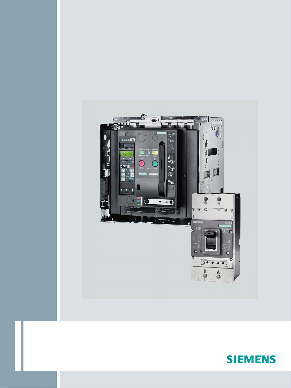
The Library SENTRON 3WL / 3VL for SIMATIC PCS 7 software package is used to connect
the circuit breakers SENTRON 3WL and 3VL to a SIMATIC PCS 7 process control system
and contains the following components:
● Block library with:
– DIA_WLVL: diagnostic block
– DRV_3WL: PCS 7 block for recording measurements, setpoints, protective
– DRV_3VL: PCS 7 block for recording measurements, setpoints, protective
– User objects and operating blocks for operating and observing measured data on the
● Online help in German and English
● Manual in German and English
The block library can be used in in the PCS 7 versions V6.1 SP1, V7.0 and V7.0 SP1.
1
parameters, etc. of a 3WL circuit-breaker
parameters, etc. of a 3VL circuit breaker
OS
1.2 Further documentation
You can find further details in the following manuals:
● Manual for SENTRON WL and SENTRON VL circuit-breakers with communication
capability
● SENTRON WL Operating Manual
● SENTRON VL Operating Manual
1.3 Installing the library
To start the installation, please insert the CD in the CD-ROM drive on your PG/PC and
launch the "Setup.exe" program. All the other information you need will be provided during
the installation process. Please also read the information in the readme file.
Library SENTRON 3WL / 3VL for SIMATIC PCS 7
Function Manual, 11/2008, A5E02316914A-01
7
Page 10
Introduction
1.4 Hardware configuration
1.4 Hardware configuration
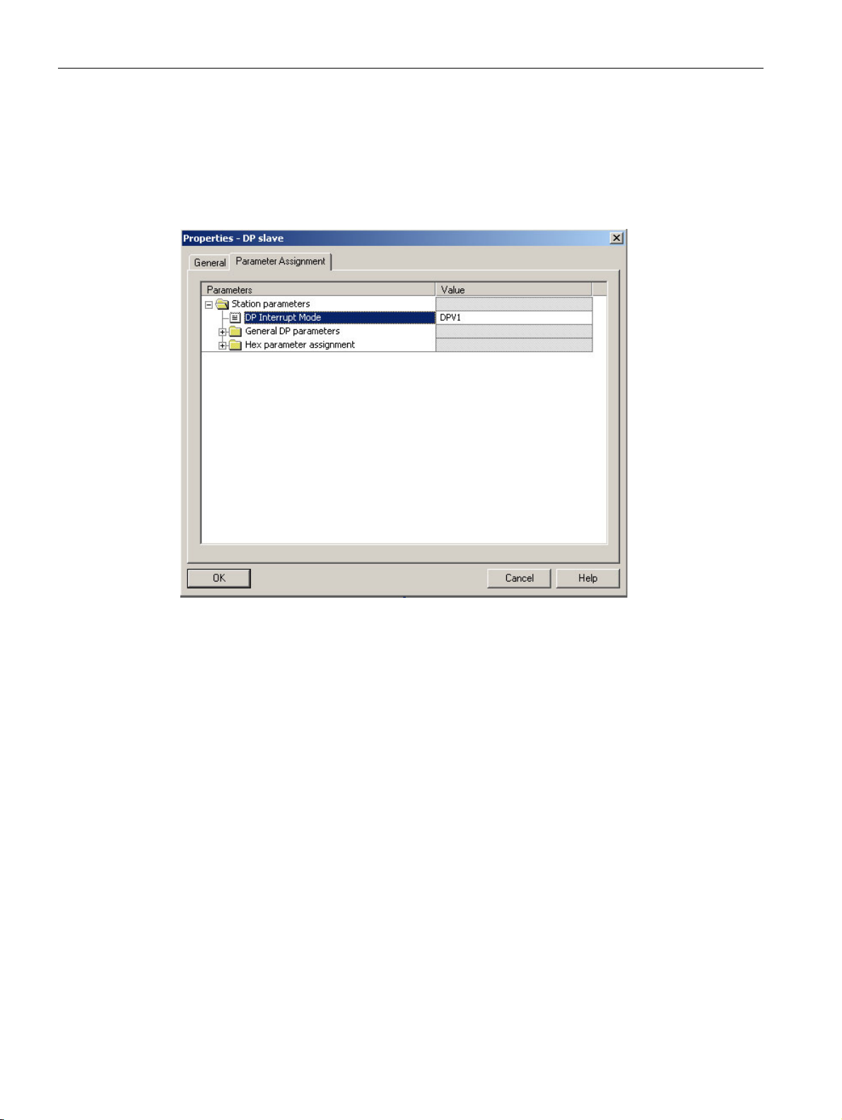
The driver concept for 3WL / 3VL supports operation of the circuit-breaker as a DP slave
directly connected to the DP master system as well as connected following a Y-link DPV0 or
DPV1.
The circuit-breakers in this setup can be incorporated using a GSD file.
NOTICE
In such cases ensure that the circuit-breaker's I/O data is within the control's process
image. This is absolutely essential to the driver generator's functionality.
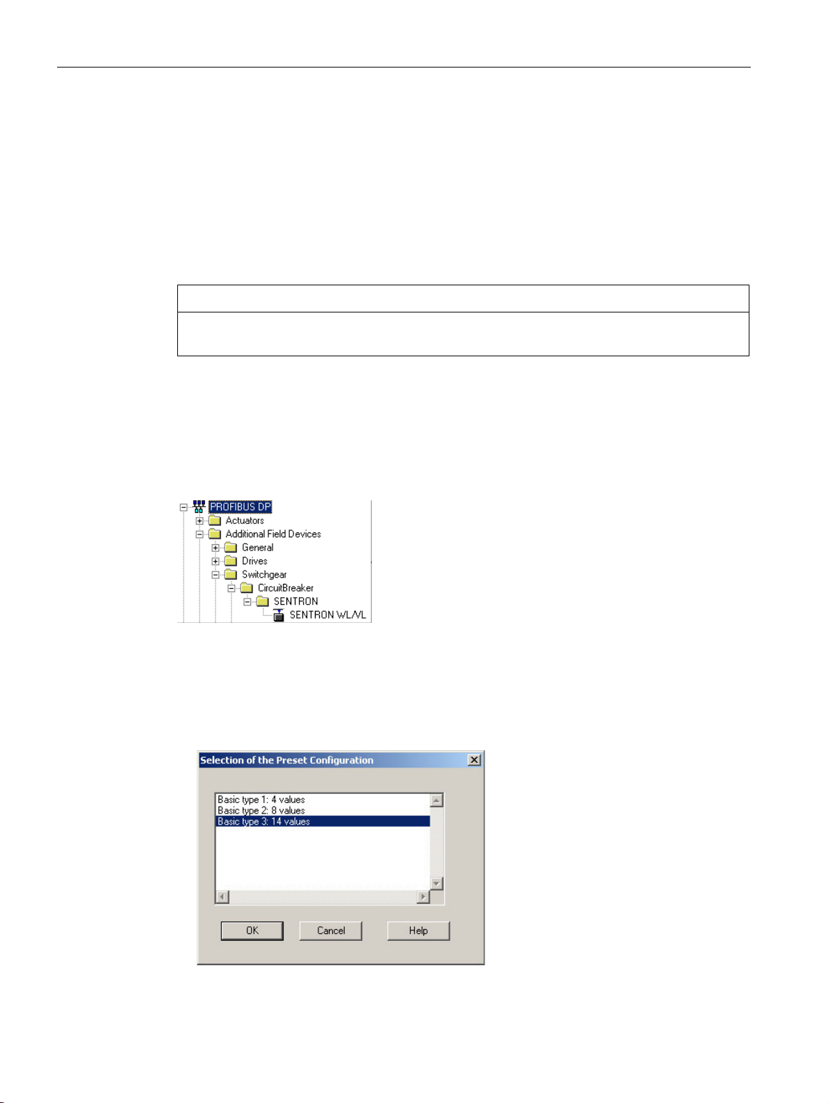
1.4.1 Incorporating via GSD file
If the 3WL / 3VL device is incorporated via GSD SIEM80C0.gsd, it is entered in the hardware
configuration catalog under PROFIBUS-DP → Other field devices → Switchgear:
Figure 1-1 Catalog path for incorporating via GSD file
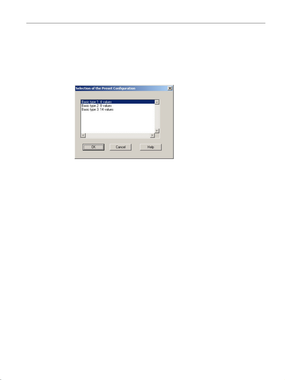
The following I/O configuration applies for 3WL:
● Outputs: 2 bytes of digital control data
● Inputs: 44 bytes of binary status (2 bytes) and measurements with property bytes (42
bytes)
Figure 1-2 Selection of basic type for 3WL
Library SENTRON 3WL / 3VL for SIMATIC PCS 7
8 Function Manual, 11/2008, A5E02316914A-01
Page 11
Introduction
1.4 Hardware configuration
This configuration corresponds to basic type 3 for 3WL. This basic type must be set to
ensure operation.
The following I/O configuration applies for 3VL:
● Outputs: 2 bytes of digital control data
● Inputs: 14 bytes of binary status (2 bytes) and measurements with property bytes (12
bytes)
Figure 1-3 Selection of basic type for 3VL
This configuration corresponds to basic type 1 for 3VL. This basic type must be set to ensure
operation.
Library SENTRON 3WL / 3VL for SIMATIC PCS 7
Function Manual, 11/2008, A5E02316914A-01
9
Page 12
Introduction
1.4 Hardware configuration
Configuration in HW config.
In the HW config., 3WL / 3VL is installed with the corresponding GSD file (see above) and
with basic type 3 and/or 1.
Figure 1-4 Properties of the 3WL / 3VL device directly connected to the DP master system
Library SENTRON 3WL / 3VL for SIMATIC PCS 7
10 Function Manual, 11/2008, A5E02316914A-01
Page 13

Introduction
1.4 Hardware configuration
If 3WL / 3VL is connected following a Y-link DPV0 or DPV1, 3WL / 3VL must be configured
in the HW config. as a DPV0 slave. All acyclic services and interrupts are deactivated. This
means that the device no longer outputs diagnostic interrupts and data records can no
longer be read from the device. For details of the effect that this has on the response of the
blocks, refer to
Section 3 Description of the blocks (Page 17).
Figure 1-5 Properties of the 3WL / 3VL device following a Y link
The start addresses of inputs and outputs must be located in the partial process image that
is assigned to the watchdog interrupt OB in which the driver block is called.
The LADDR parameter input of the driver block must be connected to the start address of
the inputs of the 3WL / 3VLdevice.
The assignment of the cyclic interface is included in the description of the driver block.
Library SENTRON 3WL / 3VL for SIMATIC PCS 7
Function Manual, 11/2008, A5E02316914A-01
11
Page 14

Introduction
1.4 Hardware configuration
Library SENTRON 3WL / 3VL for SIMATIC PCS 7
12 Function Manual, 11/2008, A5E02316914A-01
Page 15
Information about the library
2.1 Overview of the blocks
The library contains the following blocks:
Name Function Number
DIA_WLVL Diagnostic block FB1742
DRV_3WL PCS 7 driver block FB1741
DRV_3VL PCS 7 driver block FB1740
2.2 General information about OS typicals
2.2.1 Faceplates
Faceplates are configured with the Graphics Designer using the templates and PCS 7specific standard views (Trend, Batch, and Alarm) provided by the Faceplate Designer. If
other user objects and functions are required, they can be added.
2
Overview
The faceplates described are provided as functional and tested examples and can be
adapted by the user.
Two icons and a group/loop display with all the necessary displays are provided for the
driver block. The relevant group display is called using the icons.
The display forms part of the @PG_DRV_3WL_OVERVIEW.pdl / @PL_DRV_3WL.pdl
(and/or @PG_DRV_3VL_OVERVIEW.pdl / @PL_DRV_3VL.pdl) basic displays.
(1) Group display
(2) Message lock (MSG_LOCK)
(3) Message acknowledgment
(4) Message suppression (QMSG_SUP)
Figure 2-1 Section of the overview display
Library SENTRON 3WL / 3VL for SIMATIC PCS 7
Function Manual, 11/2008, A5E02316914A-01
13
Page 16

Information about the library
2.2 General information about OS typicals
Trend (@PCS7_trend.pdl)
The "ReturnPath" and "StandardTrend" properties must be parameterized on the icon to
incorporate a trend in a faceplate.
• StandardTrend
:
• ReturnPath:
2: Online values with 5 min time axis
> 2: Archive values with time axis of the value entered (in
min)
.AVGCUR Structural element name starting with a full stop
: Separators
CO_GREEN Color for trend
, Separators between two online values
Figure 2-2 Trend setting on the icon
Library SENTRON 3WL / 3VL for SIMATIC PCS 7
14 Function Manual, 11/2008, A5E02316914A-01
Page 17
Information about the library
2.2 General information about OS typicals
2.2.2 Symbols
The process display icons are based on the process symbols provided by the Faceplate
Designer. The diagrams are schematic diagrams.
Template pictures @PCS7Typicals_SENTRON.pdl / @Template_SENTRON.pdl
The icons can be found in the template diagrams @PCS7Typicals_SENTRON.pdl and
@Template_SENTRON.pdl.
When using the "Create/Update Block Icons" function, PCS 7 accesses the file
@PCS7Typicals_SENTRON.pdl .
When manually copying the icons into a process display, you must use the icons from the
@Template_SENTRON.pdl file.
Different variants of block icons
There may be several variants of block icons for one measuring point. These variants are
distinguished by the "type" attribute: The value of this attribute describes the variant. For
example, if you look at a variant of the block icon for a valve, you will find the value
"@Valve/2". You use the part of the value displayed after the "/" to control which variant of
the block icon is produced. You therefore have to enter this part in the object properties for
the block instance. If you do not enter any parameters in the object properties for the block
instance, the standard block icon is produced automatically: This is the block icon with the
"/1" label for the "type" attribute, e.g. "@Valve/1".
Only one version is however supplied per circuit breaker type with the library.
Connection to the measuring point
There is one icon for the driver block that is linked to the associated measuring point using
the "Connect picture block to tag structure" function.
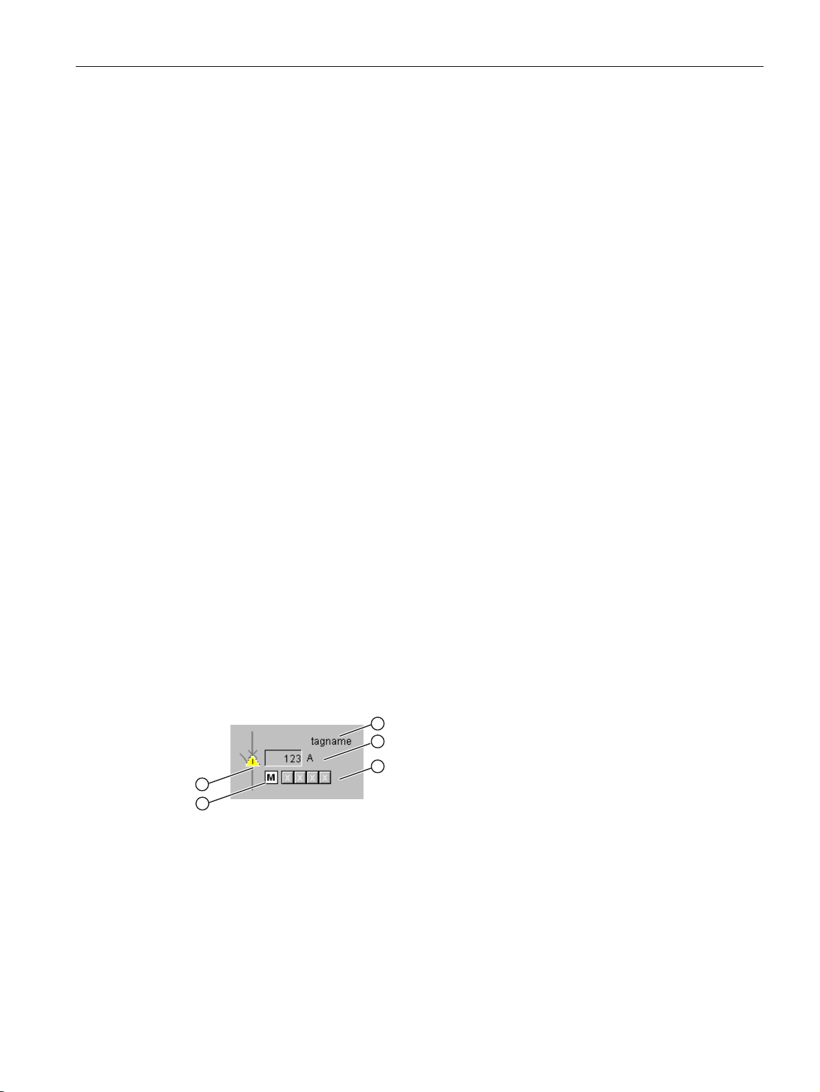
The icons contain the following visible information:
(1) Tag name
(2) Maximum phase current
(3) Group display (EventState)
(4) Circuit breaker in manual (M) / automatic (A)
(5) Circuit breaker state
Figure 2-3 Icons in Graphics Designer
Library SENTRON 3WL / 3VL for SIMATIC PCS 7
Function Manual, 11/2008, A5E02316914A-01
15
Page 18

Information about the library
2.2 General information about OS typicals
Library SENTRON 3WL / 3VL for SIMATIC PCS 7
16 Function Manual, 11/2008, A5E02316914A-01
Page 19

Description of blocks
The library consists of the blocks described below:
Diagnostic block (Page 17) DIA_WLVL
●
● Driver block (Page 22) DRV_3WL
● Driver block (Page 95) DRV_3VL
3.1 Diagnostics block DIA_WLVL
FB1742
The DRV_3WL and DRV_3VL driver blocks have a shared diagnostics block DIA_WLVL.
Description of block:
● Calling OBs (Page 18)
● Called blocks (Page 18)
● Function (Page 18)
3
See also
● Message behavior (Page 18)
● Error behavior (Page 19)
● I/O access error (Page 19)
● Module fault (Page 19)
● Read diagnostics data of 3WL / 3VL (Page 19)
● Start-up characteristics (Page 20)
● Block parameters (Page 20)
Driver module DRV_3WL (Page 22)
Driver module DRV_3VL (Page 95)
Library SENTRON 3WL / 3VL for SIMATIC PCS 7
Function Manual, 11/2008, A5E02316914A-01
17
Page 20

Description of blocks
3.1 Diagnostics block DIA_WLVL
3.1.1 Calling OBs
The block must be installed in the processing sequence in the following OBs (occurs
automatically in the CFC):
OB1 Cyclic program
OB82 Diagnostic interrupt
OB83 Insert/remove module interrupt
OB85 Program error
OB86 Rack failure
OB100 Warm restart
Installation is performed automatically by means of the function "Generate Module Driver"
3.1.2 Called blocks
The block calls the following blocks:
SFC6 RD_SINFO
SFC51 RDSYSST
3.1.3 Function
The DIA_WLVL block is responsible for diagnosis of the 3WL / 3VL device.
If a 3WL / 3VL is directly connected to the DP master system, the block evaluates the acyclic
events that are relevant for 3WL / 3VL (start-up, DP station failure, module fault), generates
quality code and diagnostic information for the MOD_PAX0 block and provides the driver
block with status information via parameter output OMODE.
In the case of operation following a Y link DPV1, diagnostic information cannot be supplied
to the driver block. The block evaluates start-up, DP station failure and module faults and
provides the driver block with this information via parameter output OMODE.
This block is not used in the case of connection following Y link DPV0.
3.1.4 Message behavior
The block has no message behavior. The messages for DP station failure and module fault
are generated by the MOD_PAX0 block (in the case of direct connection to the DP master
system) or PADP_L00 (in the case of connection following the Y link DPV0) or OB_DIAG1 (in
the case of connection following the Y link DPV1).
Library SENTRON 3WL / 3VL for SIMATIC PCS 7
18 Function Manual, 11/2008, A5E02316914A-01
Page 21

Description of blocks
3.1 Diagnostics block DIA_WLVL
3.1.5 Error behavior
Failure of the DP master or DP slave has already been determined by the previous
OB_DIAG1 block and evaluated by the RACKF, SUBN1ERR and SUBN2ERR inputs.
In the event of an error, the output OMODE features the identifier for "higher-ranking error"
(OMODE = 16#40xxxxxx).
3.1.6 I/O access error
From the viewpoint of the I/O configuration, 3WL / 3VL is a "compact" DP slave, i.e. it always
has a fixed I/O configuration. It can therefore be assumed that if an I/O access error occurs,
the entire DP slave must have failed (which is reported shortly afterwards).
I/O access errors are not evaluated any further, for this reason.
3.1.7 Module fault
Following a restart and when ACC_ID = TRUE, the module addressed with LADDR is
checked. SZL ID xC91 is read for this purpose. If the module addressed with LADDR does
not exist, the output QMODF is set and the identifier for "higher-ranking error" is entered for
the OMODE output (OMODE=16#40xxxxxx).
3.1.8 Read diagnostics data of 3WL / 3VL
If the 3WL / 3VL outputs a diagnostics alarm, system function RDSYSST (SFC51) will
activate reading of the device-specific diagnostics data.
The device-specific diagnostics data is also read out using the system function RDSYSST
(SFC51) following a CPU restart and rack start-up.
Since 3WL / 3VL following a Y link switches over to DPV0 mode, the device-specific
diagnostics data cannot be read.
The read information is transferred to the MOD_PAX0 block and the driver block where it is
evaluated.
It is also read if a request is output by the driver block at the "DIAG_REQ" input. This occurs
if:
● MAINT_MC ! = 0
● R_MAINT = 1
● Cyclically at DIAREQ_T ! = 0.0 min
The diagnostics data can also be displayed on a Maintenance Station (MS).
Library SENTRON 3WL / 3VL for SIMATIC PCS 7
Function Manual, 11/2008, A5E02316914A-01
19
Page 22

Description of blocks
3.1 Diagnostics block DIA_WLVL
Diagnostic events are assigned to maintenance status as follows:
Diagnostic event Maintenance status QUALITY PA_DIAG
Perform visual inspection on main contacts Maintenance
requirement is
medium
Immediate maintenance of main contacts
Maintenance
requirement is high
16#68 16#0020_0000
16#24 16#0100_0000
3.1.9 Start-up characteristics
In OB100, the identifier for "Start up" is entered for output OMODE (OMODE=16#xx01xxxx).
3.1.10 Block parameters
The as-supplied state of the block displayed in CFC is shown in the "I/O" column: I/O name
bold = I/O is visible, normal = I/O is invisible.
I/O (parameter) Comment Data type Default Type OCM
EN_DIAG 1 = Enable read diagnostic data BOOL FALSE I
MODE Parameter OMODE of DRV_WLVL WORD 0 I
LADDR Logical address of module INT 0 I
DADDR Diagnostic address of module INT 0 I
DPA_LINK Device connection:
0 = DP-MASTER,
1 = DP/PA-LINK
SUBN_TYP 1 = External DP interface BOOL FALSE I
SUBN1_ID ID of Primary Subnet BYTE 16#FF I
SUBN2_ID ID of Redundant Subnet BYTE 16#FF I
RACK_NO Rack number BYTE 0 I
RACKF 1 = Rack failure BOOL FALSE I
SUBN1ERR 1 = Slave 1 Failure BOOL FALSE I
SUBN2ERR 1 = Slave 2 Failure BOOL FALSE I
ACC_ID 1 = Accept new mode settings BOOL TRUE IO
DIAG_REQ 1 = Read diagnostic information BOOL FALSE I
QERR 1 = Error BOOL FALSE O
QMODF 1 = Module Failure BOOL FALSE O
QRACKF 1 = Rack failure BOOL FALSE O
RACK1ERR 1 = DP slave system failure (primary) BOOL FALSE O
RACK2ERR 1 = DP slave system failure (redundant) BOOL FALSE O
QUALITY Quality code of process value BYTE 0 O
OMODE Status MODE DWORD 0 O
BOOL FALSE I
Library SENTRON 3WL / 3VL for SIMATIC PCS 7
20 Function Manual, 11/2008, A5E02316914A-01
Page 23
Description of blocks
3.1 Diagnostics block DIA_WLVL
I/O (parameter) Comment Data type Default Type OCM
PA_DIAG Diagnostic information for maintenance DWORD 0 O
QDIAG_INF Diagnostic information WORD 0 O
Structure of OMODE
Byte Value Meaning
Byte 3 16#80: Valid data
16#40: Invalid data
Byte 2 16#01: Cold restart (OB100)
Byte 1; 0 16#0000 Irrelevant
Higher-level fault
Structure of QDIAG_INF
VALUE Meaning
0 Everything ok
1 Perform visual inspection on main contacts
2 Immediate maintenance of main contacts
Library SENTRON 3WL / 3VL for SIMATIC PCS 7
Function Manual, 11/2008, A5E02316914A-01
21
Page 24

Description of blocks
3.2 Driver module DRV_3WL
3.2 Driver module DRV_3WL
FB1741
Description of block:
● Calling OBs (Page 22)
● Called blocks (Page 23)
● Function (Page 23)
● Message behavior (Page 26)
● Assignment of the cyclic process image (Page 27)
● Addressing and module driver (Page 28)
● Processing the diagnostics data of the 3WL de
● Start-up characteristics (Page 29)
● Block parameters (Page 29)
● Description of symbols a
See also
Diagnostics block DIA_WLVL (Page 17)
Driver module DRV_3VL (Page 95)
3.2.1 Calling OBs
The OB watchdog interrupt in which the block is installed (e.g. OB32). Also in OB100
(performed automatically in CFC, see start-up characteristics).
vice (Page 28)
nd faceplates (Page 60)
Library SENTRON 3WL / 3VL for SIMATIC PCS 7
22 Function Manual, 11/2008, A5E02316914A-01
Page 25

Description of blocks
3.2 Driver module DRV_3WL
3.2.2 Called blocks
The block calls the following blocks:
SFB35 ALARM_8P
SFB52 RDREC
SFB53 WRREC
SFC1 READ_CLK
SFC6 RD_SINFO
SFC20 BLKMOV
SFC21 FILL
3.2.3 Function
The DRV_3WL block is used for measurement acquisition and control and it forms the
interface to the OS.
Automatic / manual mode switch over
Automatic and manual mode are available for operating the driver block. When in manual
mode, the user can control the circuit breaker position (ON / OFF) of the faceplate in WinCC.
When in automatic mode, the corresponding buttons are locked (cannot be operated) in the
faceplate and the circuit breaker is controlled by input parameters which can be connected in
the CFC (AUTO_ON / AUTO_OFF) and therefore by the AS program.
The user can define the mode in which the block is to run in the faceplate or in a block
parameter (AUT_L).
The setting at the LIOP_SEL input determines which of the parameters is currently active.
NOTICE
If an error occurs (monitoring error, Local turn off, Tripped) the block changes to Forced
manual. If the pending error state is acknowledged with one of the RESET buttons, the
block goes into the specified mode again.
If Automatic mode is specified by the AS program (LIOP_SEL = 1, AUT_L = 1) the
commands present at AUTO_ON or AUTO_OFF are always output.
Under certain circumstances this means that resetting error states may cause a switching
operation of the circuit breaker. If this is not desired the user must configure the AS
program accordingly.
Library SENTRON 3WL / 3VL for SIMATIC PCS 7
Function Manual, 11/2008, A5E02316914A-01
23
Page 26

Description of blocks
3.2 Driver module DRV_3WL
Switching the circuit breaker on/off
The user can use the driver block to switch the circuit breaker.
It is important to note here that the ON state means "main contacts closed" and the OFF
state means "main contacts open".
The circuit breaker cannot be switched on or off in certain states:
It must not be switched on when:
• there is a monitoring error
• the block is in maintenance mode
• write protection applies
• the circuit breaker is already on
• the circuit breaker has tripped
• the circuit breaker has been switched off locally
• the circuit breaker is not ready for an On command
(QMON_ERR = 1)
(MAINT = 1)
(QWR_PROT = 1)
(QON = 1)
(QTRIP = 1)
(QLOC_OFF = 1)
(RDY_ON = 0)
It must not be switched off when:
• there is a monitoring error
• the block is in maintenance mode
• write protection applies
• the circuit breaker is already off
• the circuit breaker has tripped
• the circuit breaker has been switched off locally
Resetting Tripped and Local turn off states
If the block is in one of the two states, it has to be reset before an On command can be
output again. The faceplate features a corresponding button for the user for this RESET.
CAUTION
Before the circuit breaker is switched back on, the reason for tripping/switching off must be
established and possible error causes must be rectified.
NOTICE
If such a state is reset the response of the mode must be observed as it may cause a
switching operation of the circuit breaker under certain circumstances.
(QMON_ERR = 1)
(MAINT = 1)
(QWR_PROT = 1)
(QOFF = 1)
(QTRIP = 1)
(QLOC_OFF = 1)
See Automatic / Manual mode switchover
Library SENTRON 3WL / 3VL for SIMATIC PCS 7
24 Function Manual, 11/2008, A5E02316914A-01
Page 27

Description of blocks
3.2 Driver module DRV_3WL
Feedback monitoring
When monitoring is activated (MONITOR = On), switching commands (ON / OFF) and the
resetting of trips are time monitored. If the expected state is not reached after an operation
and within the monitoring time (TIME_MON), the block outputs a message and goes into a
resetting state (QMON_ERR).
NOTICE
If the monitoring error is reset the response of the mode must be observed as it may cause
a switching operation of the circuit breaker under certain circumstances.
See Automatic / Manual mode switchover
The faceplate features an appropriate RESET button for resetting this state again.
Measured value acquisition
The block reads measured values from the cyclic process image.
When operating 3WL on the DP master system directly, the block also reads data record 94
with the system function block RDREC (SFB52).
The data record is read in a defined cycle. The interval at which the data record can be read
can be set in seconds using the input parameter CYCLE_T. The default setting is 60
seconds. A cycle of 0 seconds or less means that this data record is not read.
Time synchronization
Data record 68 writes the current time in cycles in order to transfer the current time to the
circuit breaker. This cycle can be set in seconds using the TIME_SYNC_T parameter.
Diagnostics and maintenance
In order to display the current state of the circuit breaker, modules present, statistics
information and diagnostic messages, the module reads the status word from the process
image and data records 91 and 92.
The process image is called in cycles. The user can request the data records in the faceplate
Library SENTRON 3WL / 3VL for SIMATIC PCS 7
Function Manual, 11/2008, A5E02316914A-01
via operations. The diagnostic messages are updated in cycles when messages are present.
WARNING
During maintenance work on the circuit breaker, maintenance mode must be activated!
At the same time, the circuit breaker must be locked locally to prevent it being switched
back on.
Maintenance specifications apply to the circuit breakers (in accordance with EN 50 110-1,
DIN VDE 0105-100 and BGV A2).
25
Page 28

Description of blocks
3.2 Driver module DRV_3WL
Protect. parameter and extended protect. parameter
This data, which comes from data records 128 and 129, is updated for the display in the
faceplate if requested by the operator.
These parameters cannot be written.
Setpoints
These parameters can be read and written from the faceplate.
3.2.4 Message behavior
DRV_3WL issues the following messages:
Message block Message
number
MSG_EVID1
MSG_EVID2
1 Overload tripping (L) AH
2 Instantaneous short-circuit (I) AH
3 Short-time-delay short-circuit (S) AH
4 Ground fault (G) AH
5 Trip as a result of extended protection function AH
6 Overload in neutral conductor AH
7 Overload warning present WH
8 An activated setpoint value has been exceeded WH
1 An alarm signal is currently present WH
2 Error time synchronization WH
3 Local turn off of circuit breaker / tripped AH
4 Load shedding warning WH
5 Perform visual inspection on main contacts WH
6 Immediate maintenance of main contacts AH
7 Monitoring error AS Control System
8 Forbidden switching command for auto mode - switching
Message text Message class
Fault
AS Control System
command ignored
Fault
Library SENTRON 3WL / 3VL for SIMATIC PCS 7
26 Function Manual, 11/2008, A5E02316914A-01
Page 29

Description of blocks
3.2 Driver module DRV_3WL
Auxiliary values
EV_ID Auxiliary value Block parameters
MSG_EVID1
-
MSG_EVID2
1 AUX_PR01
2 AUX_PR02
3 AUX_PR03
4 AUX_PR04
5 AUX_PR05
6 AUX_PR06
7 AUX_PR07
8 AUX_PR08
9 AUX_PR09
10 AUX_PR10
3.2.5 Assignment of the cyclic process image
Only basic type 3 is supported in the default setting.
Name Inputs Outputs
0 / 1 Control bytes 2
0 / 1 Binary status information 2
2 / 3 Current in phase 1 2
4 / 5 Current in phase 2 2
6 / 7 Current in phase 3 2
8 / 9 Max. current in phase under highest load 2
10 / 11 Current in neutral conductor 2
12 / 13 Phase-to-phase voltage L12 2
14 / 15 Phase-to-phase voltage L23 2
16 / 17 Phase-to-phase voltage L31 2
18 / 19 Neutral-point star voltage L1N 2
20 / 21 Neutral-point star voltage L2N 2
22 / 23 Neutral-point star voltage L3N 2
24 / 25 Mean value of power factors of 3 phases 2
26 / 27 Total active energy of 3 phases 2
28 / 29 Total apparent power of 3 phases 2
30 EB of current phase 1 1
31 EB of current phase 2 1
32 EB of current phase 3 1
33 EB of max. current in phase under highest load 1
34 EB of current in neutral conductor 1
35 EB of phase-to-phase voltage L12 1
Library SENTRON 3WL / 3VL for SIMATIC PCS 7
Function Manual, 11/2008, A5E02316914A-01
27
Page 30

Description of blocks
3.2 Driver module DRV_3WL
Name Inputs Outputs
36 EB of phase-to-phase voltage L23 1
37 EB of phase-to-phase voltage L31 1
38 EB of neutral-point star voltage L1N 1
39 EB of neutral-point star voltage L2N 1
40 EB of neutral-point star voltage L3N 1
41 EB of mean value of the three power factors 1
42 EB of total active energy 1
43 EB of total apparent power 1
Number of bytes 44 2
3.2.6 Addressing and module driver
The I/O addresses of 3WL must lie completely within the process image of the CPU. In the
CFC chart, the LADDR input is connected to the base address of the 3WL device.
Procedure:
Select input parameter → right mouse button → Interconnection to
address... → Entere.g. EW512
If 3WL is directly connected to the DP master system, the module driver connects block
outputs OMODE, QRACKF and QMODF to inputs MODE00, RACKF and MODF of the block
MOD_PAX0 and the module driver connects input DIAG_INF to output QDIAG_INF of
diagnostics block DIA_WLVL.
In the case of operation following a Y-Link DPV1, the module driver connects block inputs
MODE, RACKF and DIAG_INF to outputs OMODE, QRACKF and QDIAG_INF of
diagnostics block DIA_WLVL.
In the case of operation following a Y-Link DPV0, the module driver connects block inputs
MODE and RACKF to outputs OMODE00 and QRACKF of block PADP_L00.
The block input BASADR is parameterized with the logical base address of the 3WL device
by the module driver.
The block input BASADR_OUT is parameterized with the start address of the outputs of the
3WL device by the module driver.
The input DPA_LINK is parameterized with the connection mode of the 3WL device by the
module driver.
● DPA_LINK = 0 -> Directly connected to the DP master
● DPA_LINK = 1 -> Connected following a DP/PA link
3.2.7 Processing the diagnostics data of the 3WL device
If 3WL is directly connected to the DP master system, the block processes the diagnostic
information that is supplied to it from the DIA_WLVL diagnostics block via the input
DIAG_INF.
The user has the possibility of setting the cycle for cyclic reading of the diagnostics data
record at the "DIAREQ_T" input. At DIAREQ_T = 0.0 minutes no cyclic reading takes place.
Library SENTRON 3WL / 3VL for SIMATIC PCS 7
28 Function Manual, 11/2008, A5E02316914A-01
Page 31

Description of blocks
3.2 Driver module DRV_3WL
3.2.8 Start-up characteristics
On starting, messages are deactivated (OB100).
3.2.9 Block parameters
The as-supplied state of the block displayed in CFC is shown in the "I/O" column: I/O name
bold = I/O is visible, normal = I/O is invisible.
I/O (parameter) Comment Data type Default Type OCM
MODE Parameter OMODE of DIA_WLVL DWORD 0 I
RACKF 1 = Rack failure BOOL FALSE I
LADDR Base address of 3WL module WORD 0 I
BASADR Base address of 3WL module INT 0 I
BASADR_OUT Base address of 3WL module for outputs INT 0 I
DPA_LINK Device connection: 0 = DP-MASTER,
1 = DP/PA-LINK
MSG_LOCK 1 = Messages locked BOOL FALSE I x
RUNUPCYC Lag: Number of run up cycles INT 0 I
SAMPLE_T Sample time [s] REAL 0.0 I
CYCLE_T Cycle time of cyclic reading of DRs [s] REAL 60.0 I
TIME_SYNC_T Cycle time of time synchronization [min] REAL 10.0 I
DIAREQ_T Cycle time of reading diagnostic
information [min]
DR94_K 1 = kWh inputs for real and reactive energy
of DR 94 are used
MONITOR 1 = Monitoring activated BOOL TRUE I
TIME_MON Monitoring time [s] REAL 10.0 I
DIAG_INF Diagnostic info for driver WORD 0 I
ALT_SYM 1 = Alternative symbols BOOL FALSE I
MANOP_EN 1 = Operator may input MANUAL BOOL TRUE I
AUTOP_EN 1 = Operator may input AUTO BOOL TRUE I
LIOP_SEL 1 = Linking, 0 = Operator active BOOL FALSE I
AUT_L Linkable input for MANUAL/AUTO mode BOOL FALSE I
AUTO_ON AUTO mode: Switch off (open the main
contacts)
AUTO_OFF AUTO mode: Switch on (close the main
contacts)
MSG_EVID1 Message ID message block 1 DWORD 0 I
MSG_EVID2 Message ID message block 2 DWORD 0 I
SUP_OVLD_WRN 1 = Active message suppression BOOL FALSE I x
SUP_SP_EXCEED 1 = Active message suppression BOOL FALSE I x
SUP_WRN 1 = Active message suppression BOOL FALSE I x
SUP_LD_SHED 1 = Active message suppression BOOL FALSE I x
BOOL FALSE I x
BOOL FALSE O
BOOL FALSE I x
BOOL FALSE I
BOOL FALSE I
Library SENTRON 3WL / 3VL for SIMATIC PCS 7
Function Manual, 11/2008, A5E02316914A-01
29
Page 32

Description of blocks
3.2 Driver module DRV_3WL
I/O (parameter) Comment Data type Default Type OCM
RP_NORM_I DR 130: Real power in normal direction REAL 0.0 I x
RP_NORM_I_QC Quality code of RP_NORM_I BYTE 0 I
RP_NORM_I_OFF DR 130: Real power in normal direction
OFF
RP_NORM_I_NA DR 130: Real power in normal direction
not available
RP_REV_I DR 130: Real power in reverse direction REAL 0.0 I x
RP_REV_I_QC Quality code of RP_REV_I BYTE 0 I
RP_REV_I_OFF DR 130: Real power in reverse direction
OFF
RP_REV_I_NA DR 130: Real power in reverse direction
not available
PF_CAP_I DR 130: Power factor capacitive REAL 0.0 I x
PF_CAP_I_QC Quality code of PF_CAP_I BYTE 0 I
PF_CAP_I_OFF DR 130: Power factor capacitive OFF BOOL FALSE I x
PF_CAP_I_NA DR 130: Power factor capacitive not
available
PF_IND_I DR 130: Power factor inductive REAL 0.0 I x
PF_IND_I_QC Quality code of PF_IND_I BYTE 0 I
PF_IND_I_OFF DR 130: Power factor inductive OFF BOOL FALSE I x
PF_IND_I_NA DR 130: Power factor inductive not
available
T_RP_NORM_I DR 130: Delay time for real power in
normal direction
T_RP_NORM_I_QC Quality code of T_RP_NORM_I BYTE 0 I
T_RP_NORM_I_OFF DR 130: Delay time for real power in
normal direction OFF
T_RP_NORM_I_NA DR 130: Delay time for real power in
normal direction not available
T_RP_REV_I DR 130: Delay time for real power in
reverse direction
T_RP_REV_I_QC Quality code of T_RP_REV_I BYTE 0 I
T_RP_REV_I_OFF DR 130: Delay time for real power in
reverse direction OFF
T_RP_REV_I_NA DR 130: Delay time for real power in
reverse direction not available
T_PF_CAP_I DR 130: Delay time for power factor
capacitive
T_PF_CAP_I_QC Quality code of T_PF_CAP_I BYTE 0 I
T_PF_CAP_I_OFF DR 130: Delay time for power factor
capacitive OFF
T_PF_CAP_I_NA DR 130: Delay time for power factor
capacitive not available
T_PF_IND_I DR 130: Delay time for power factor
inductive
T_PF_IND_I_QC Quality code of T_PF_IND_I BYTE 0 I
BOOL FALSE I x
BOOL FALSE I x
BOOL FALSE I x
BOOL FALSE I x
BOOL FALSE I x
BOOL FALSE I x
REAL 0.0 I x
BOOL FALSE I x
BOOL FALSE I x
REAL 0.0 I x
BOOL FALSE I x
BOOL FALSE I x
REAL 0.0 I x
BOOL FALSE I x
BOOL FALSE I x
REAL 0.0 I x
Library SENTRON 3WL / 3VL for SIMATIC PCS 7
30 Function Manual, 11/2008, A5E02316914A-01
Page 33

Description of blocks
3.2 Driver module DRV_3WL
I/O (parameter) Comment Data type Default Type OCM
T_PF_IND_I_OFF DR 130: Delay time for power factor
inductive OFF
T_PF_IND_I_NA DR 130: Delay time for power factor
inductive not available
OVER_FRQ_I DR 130: Over frequency REAL 0.0 I x
OVER_FRQ_I_QC Quality code of OVER_FRQ_I BYTE 0 I
OVER_FRQ_I_OFF DR 130: Over frequency OFF BOOL FALSE I x
OVER_FRQ_I_NA DR 130: Over frequency not available BOOL FALSE I x
T_OVER_FRQ_I DR 130: Delay time for over frequency REAL 0.0 I x
T_OVER_FRQ_I_QC Quality code of T_OVER_FRQ_I BYTE 0 I
T_OVER_FRQ_I_OFF DR 130: Delay time for over frequency
OFF
T_OVER_FRQ_I_NA DR 130: Delay time for over frequency not
available
UNDER_FRQ_I DR 130: Under frequency REAL 0.0 I x
UNDER_FRQ_I_QC Quality code of UNDER_FRQ_I BYTE 0 I
UNDER_FRQ_I_OFF DR 130: Under frequency OFF BOOL FALSE I x
UNDER_FRQ_I_NA DR 130: Under frequency not available BOOL FALSE I x
T_UNDER_FRQ_I DR 130: Delay time for under frequency REAL 0.0 I x
T_UNDER_FRQ_I_QC Quality code of T_UNDER_FRQ_I BYTE 0 I
T_UNDER_FRQ_I_OFF DR 130: Delay time for under frequency
OFF
T_UNDER_FRQ_I_NA DR 130: Delay time for under frequency
not available
CUR_THD_I DR 130: THD current REAL 0.0 I x
CUR_THD_I_QC Quality code of CUR_THD_I BYTE 0 I
CUR_THD_I_OFF DR 130: THD current OFF BOOL FALSE I x
CUR_THD_I_NA DR 130: THD current not available BOOL FALSE I x
T_CUR_THD_I DR 130: Delay time for THD current REAL 0.0 I x
T_CUR_THD_I_QC Quality code of T_CUR_THD_I BYTE 0 I
T_CUR_THD_I_OFF DR 130: Delay time for THD current OFF BOOL FALSE I x
T_CUR_THD_I_NA DR 130: Delay time for THD current not
available
VOLT_THD_I DR 130: THD voltage REAL 0.0 I x
VOLT_THD_I_QC Quality code of VOLT_THD_I BYTE 0 I
VOLT_THD_I_OFF DR 130: THD voltage OFF BOOL FALSE I x
VOLT_THD_I_NA DR 130: THD voltage not available BOOL FALSE I x
T_VOLT_THD_I DR 130: Delay time for THD voltage REAL 0.0 I x
T_VOLT_THD_I_QC Quality code of T_VOLT_THD_I BYTE 0 I
T_VOLT_THD_I_OFF DR 130: Delay time for THD voltage OFF BOOL FALSE I x
T_VOLT_THD_I_NA DR 130: Delay time for THD voltage not
available
CREST_F_I DR 130: Crest factor REAL 0.0 I x
CREST_F_I_QC Quality code of CREST_F_I BYTE 0 I
BOOL FALSE I x
BOOL FALSE I x
BOOL FALSE I x
BOOL FALSE I x
BOOL FALSE I x
BOOL FALSE I x
BOOL FALSE I x
BOOL FALSE I x
Library SENTRON 3WL / 3VL for SIMATIC PCS 7
Function Manual, 11/2008, A5E02316914A-01
31
Page 34

Description of blocks
3.2 Driver module DRV_3WL
I/O (parameter) Comment Data type Default Type OCM
CREST_F_I_OFF DR 130: Crest factor OFF BOOL FALSE I x
CREST_F_I_NA DR 130: Crest factor not available BOOL FALSE I x
FORM_F_I DR 130: Form factor REAL 0.0 I x
FORM_F_I_QC Quality code of FORM_F_I BYTE 0 I
FORM_F_I_OFF DR 130: Form factor OFF BOOL FALSE I x
FORM_F_I_NA DR 130: Form factor not available BOOL FALSE I x
T_CREST_F_I DR 130: Delay time for crest factor REAL 0.0 I x
T_CREST_F_I_QC Quality code of T_CREST_F_I BYTE 0 I
T_CREST_F_I_OFF DR 130: Delay time for crest factor OFF BOOL FALSE I x
T_CREST_F_I_NA DR 130: Delay time for crest factor not
available
T_FORM_F_I DR 130: Delay time for form factor REAL 0.0 I x
T_FORM_F_I_QC Quality code of T_FORM_F_I BYTE 0 I
T_FORM_F_I_OFF DR 130: Delay time for form factor OFF BOOL FALSE I x
T_FORM_F_I_NA DR 130: Delay time for form factor not
available
RP_DEM_I DR 130: Demand real power REAL 0.0 I x
RP_DEM_I_QC Quality code of PR_DEM_I BYTE 0 I
RP_DEM_I_OFF DR 130: Demand real power OFF BOOL FALSE I x
RP_DEM_I_NA DR 130: Demand real power not available BOOL FALSE I x
AP_DEM_I DR 130: Demand apparent power REAL 0.0 I x
AP_DEM_I_QC Quality code of AP_DEM_I BYTE 0 I
AP_DEM_I_OFF DR 130: Demand apparent power OFF BOOL FALSE I x
AP_DEM_I_NA DR 130: Demand apparent power not
available
T_RP_DEM_I DR 130: Delay time demand of the real
power
T_RP_DEM_I_QC Quality code of T_RP_DEM_I BYTE 0 I
T_RP_DEM_I_OFF DR 130: Delay time demand of the real
power OFF
T_RP_DEM_I_NA DR 130: Delay time demand of the real
power not available
T_AP_DEM_I DR 130: Delay time demand of the
apparent power
T_AP_DEM_I_QC Quality code of T_AP_DEM_I BYTE 0 I
T_AP_DEM_I_OFF DR 130: Delay time demand of the
apparent power OFF
T_AP_DEM_I_NA DR 130: Delay time demand of the
apparent power not available
RAP_DEM_I DR 130: Demand reactive power REAL 0.0 I x
RAP_DEM_I_QC Quality code of RAP_DEM_I BYTE 0 I
RAP_DEM_I_OFF DR 130: Demand reactive power OFF BOOL FALSE I x
RAP_DEM_I_NA DR 130: Demand reactive power not
Available
BOOL FALSE I x
BOOL FALSE I x
BOOL FALSE I x
REAL 0.0 I x
BOOL FALSE I x
BOOL FALSE I x
REAL 0.0 I x
BOOL FALSE I x
BOOL FALSE I x
BOOL FALSE I x
Library SENTRON 3WL / 3VL for SIMATIC PCS 7
32 Function Manual, 11/2008, A5E02316914A-01
Page 35

Description of blocks
3.2 Driver module DRV_3WL
I/O (parameter) Comment Data type Default Type OCM
RAP_NORM_I DR 130: Reactive power in normal
direction
RAP_NORM_I_QC Quality code of RAP_NORM_I BYTE 0 I
RAP_NORM_I_OFF DR 130: Reactive power in normal
direction OFF
RAP_NORM_I_NA DR 130: Reactive power in normal
direction not available
T_RAP_DEM_I DR 130: Delay time demand of the
reactive power
T_RAP_DEM_I_QC Quality code of T_RAP_DEM_I BYTE 0 I
T_RAP_DEM_I_OFF DR 130: Delay time demand of the
reactive power OFF
T_RAP_DEM_I_NA DR 130: Delay time demand of the
reactive power not available
T_RAP_NORM_I DR 130: Delay time for reactive power in
normal direction
T_RAP_NORM_I_QC Quality code of T_RAP_NORM_I BYTE 0 I
T_RAP_NORM_I_OFF DR 130: Delay time for reactive power in
normal direction OFF
T_RAP_NORM_I_NA DR 130: Delay time for reactive power in
normal direction not available
RAP_REV_I DR 130: Reactive power in reverse
direction
RAP_REV_I_QC Quality code of RAP_REV_I BYTE 0 I
RAP_REV_I_OFF DR 130: Reactive power in reverse
direction OFF
RAP_REV_I_NA DR 130: Reactive power in reverse
direction not available
AP_I DR 130: Apparent power REAL 0.0 I x
AP_I_QC Quality code of AP_I BYTE 0 I
AP_I_OFF DR 130: Apparent power OFF BOOL FALSE I x
AP_I_NA DR 130: Apparent power not available BOOL FALSE I x
T_RAP_REV_I DR 130: Delay time for reactive power in
reverse direction
T_RAP_REV_I_QC Quality code of T_RAP_REV_I BYTE 0 I
T_RAP_REV_I_OFF DR 130: Delay time for reactive power in
reverse direction OFF
T_RAP_REV_I_NA DR 130: Delay time for reactive power in
reverse direction not available
T_AP_I DR 130: Delay time for apparent power REAL 0.0 I x
T_AP_I_QC Quality code of T_AP_I BYTE 0 I
T_AP_I_OFF DR 130: Delay time for apparent power
OFF
T_AP_I_NA DR 130: Delay time for apparent power not
available
CUR_OVER_I DR 130: Over current REAL 0.0 I x
REAL 0.0 I x
BOOL FALSE I x
BOOL FALSE I x
REAL 0.0 I x
BOOL FALSE I x
BOOL FALSE I x
REAL 0.0 I x
BOOL FALSE I x
BOOL FALSE I x
REAL 0.0 I x
BOOL FALSE I x
BOOL FALSE I x
REAL 0.0 I x
BOOL FALSE I x
BOOL FALSE I x
BOOL FALSE I x
BOOL FALSE I x
Library SENTRON 3WL / 3VL for SIMATIC PCS 7
Function Manual, 11/2008, A5E02316914A-01
33
Page 36

Description of blocks
3.2 Driver module DRV_3WL
I/O (parameter) Comment Data type Default Type OCM
CUR_OVER_I_QC Quality code of CUR_OVER_I BYTE 0 I
CUR_OVER_I_OFF DR 130: Over current OFF BOOL FALSE I x
CUR_OVER_I_NA DR 130: Over current not available BOOL FALSE I x
CUR_GRD_I DR 130: Earth fault current REAL 0.0 I x
CUR_GRD_I_QC Quality code of CUR_GRD_I BYTE 0 I
CUR_GRD_I_OFF DR 130: Earth fault current OFF BOOL FALSE I x
CUR_GRD_I_NA DR 130: Earth fault current not available BOOL FALSE I x
CUR_N_I DR 130: Over current N-phase REAL 0.0 I x
CUR_N_I_QC Quality code of CUR_N_I BYTE 0 I
CUR_N_I_OFF DR 130: Over current N-phase OFF BOOL FALSE I x
CUR_N_I_NA DR 130: Over current N-phase not
available
CUR_DEM_I DR 130: Demand of the current REAL 0.0 I x
CUR_DEM_I_QC Quality code of CUR_DEM_I BYTE 0 I
CUR_DEM_I_OFF DR 130: Demand of the current OFF BOOL FALSE I x
CUR_DEM_I_NA DR 130: Demand of the current not
available
T_CUR_OVER_I DR 130: Delay time for over current REAL 0.0 I x
T_CUR_OVER_I_QC Quality code of T_CUR_OVER_I BYTE 0 I
T_CUR_OVER_I_OFF DR 130: Delay time for over current OFF BOOL FALSE I x
T_CUR_OVER_I_NA DR 130: Delay time for over current not
available
T_CUR_GRD_I DR 130: Delay time for over current
ground
T_CUR_GRD_I_QC Quality code of T_CUR_GRD_I BYTE 0 I
T_CUR_GRD_I_OFF DR 130: Delay time for over current
ground OFF
T_CUR_GRD_I_NA DR 130: Delay time for over current
ground not available
T_CUR_N_I DR 130: Delay time for over current N-
phase
T_CUR_N_I_QC Quality code of T_CUR_N_I BYTE 0 I
T_CUR_N_I_OFF DR 130: Delay time for over current N-
phase OFF
T_CUR_N_I_NA DR 130: Delay time for over current N-
phase not available
UNBAL_CUR_I DR 130: Phase unbalance current REAL 0.0 I x
UNBAL_CUR_I_QC Quality code of UNBAL_CUR_I BYTE 0 I
UNBAL_CUR_I_OFF DR 130: Phase unbalance current OFF BOOL FALSE I x
UNBAL_CUR_I_NA DR 130: Phase unbalance current not
available
T_UNBAL_CUR_I DR 130: Delay time for phase unbalance
current
T_UNBAL_CUR_I_QC Quality code of T_UNBAL_CUR_I BYTE 0 I
BOOL FALSE I x
BOOL FALSE I x
BOOL FALSE I x
REAL 0.0 I x
BOOL FALSE I x
BOOL FALSE I x
REAL 0.0 I x
BOOL FALSE I x
BOOL FALSE I x
BOOL FALSE I x
REAL 0.0 I x
Library SENTRON 3WL / 3VL for SIMATIC PCS 7
34 Function Manual, 11/2008, A5E02316914A-01
Page 37

Description of blocks
3.2 Driver module DRV_3WL
I/O (parameter) Comment Data type Default Type OCM
T_UNBAL_CUR_I_OFF DR 130: Delay time for phase unbalance
current OFF
T_UNBAL_CUR_I_NA DR 130: Delay time for phase unbalance
current not available
T_CUR_DEM_I DR 130: Delay time for demand of the
current
T_CUR_DEM_I_QC Quality code of T_CUR_DEM_I BYTE 0 I
T_CUR_DEM_I_OFF DR 130: Delay time for demand of the
current OFF
T_CUR_DEM_I_NA DR 130: Delay time for demand of the
current not available
UNDER_VOLT_I DR 130: Under voltage REAL 0.0 I x
UNDER_VOLT_I_QC Quality code of UNDER_VOLT_I BYTE 0 I
UNDER_VOLT_I_OFF DR 130: Under voltage OFF BOOL FALSE I x
UNDER_VOLT_I_NA DR 130: Under voltage not available BOOL FALSE I x
T_UNDER_VOLT_I DR 130: Delay time for under voltage REAL 0.0 I x
T_UNDER_VOLT_I_QC Quality code of T_UNDER_VOLT_I BYTE 0 I
T_UNDER_VOLT_I_OFF DR 130: Delay time for under voltage OFF BOOL FALSE I x
T_UNDER_VOLT_I_NA DR 130: Delay time for under voltage not
available
UNBAL_VOLT_I DR 130: Phase unbalance voltage REAL 0.0 I x
UNBAL_VOLT_I_QC Quality code of UNBAL_VOLT_I BYTE 0 I
UNBAL_VOLT_I_OFF DR 130: Phase unbalance voltage OFF BOOL FALSE I x
UNBAL_VOLT_I_NA DR 130: Phase unbalance voltage not
available
T_UNBAL_VOLT_I DR 130: Delay time for phase unbalance
voltage
T_UNBAL_VOLT_I_QC Quality code of T_UNBAL_VOLT_I BYTE 0 I
T_UNBAL_VOLT_I_OFF DR 130: Delay time for phase unbalance
voltage OFF
T_UNBAL_VOLT_I_NA DR 130: Delay time for phase unbalance
voltage not available
OVER_VOLT_I DR 130: Over voltage REAL 0.0 I x
OVER_VOLT_I_QC Quality code of OVER_VOLT_I BYTE 0 I
OVER_VOLT_I_OFF DR 130: Over voltage OFF BOOL FALSE I x
OVER_VOLT_I_NA DR 130: Over voltage not available BOOL FALSE I x
T_OVER_VOLT_I DR 130: Delay time for over voltage REAL 0.0 I x
T_OVER_VOLT_I_QC Quality code of T_OVER_VOLT_I BYTE 0 I
T_OVER_VOLT_I_OFF DR 130: Delay time for over voltage OFF BOOL FALSE I x
T_OVER_VOLT_I_NA DR 130: Delay time for over voltage not
available
RD_DR69 Read data record 69 (status of the
modules)
RD_DR91 Read data record 91 (statistic and
maintenance)
BOOL FALSE I x
BOOL FALSE I x
REAL 0.0 I x
BOOL FALSE I x
BOOL FALSE I x
BOOL FALSE I x
BOOL FALSE I x
REAL 0.0 I x
BOOL FALSE I x
BOOL FALSE I x
BOOL FALSE I x
BOOL FALSE IO x
BOOL FALSE IO x
Library SENTRON 3WL / 3VL for SIMATIC PCS 7
Function Manual, 11/2008, A5E02316914A-01
35
Page 38

Description of blocks
3.2 Driver module DRV_3WL
I/O (parameter) Comment Data type Default Type OCM
RD_DR92 Read data record 92 (diagnostics) BOOL FALSE IO x
RD_DR128 Read data record 128 (metering and ext.
protective function)
RD_DR129 Read data record 129 (protective function) BOOL FALSE IO x
RD_DR130 Read data record 130 (setpoints) BOOL FALSE IO x
WR_DR130 Write data record 130 (setpoints) BOOL FALSE IO x
AUT_ON_OP Operator input: Mode 1 = AUTO,
0 = MANUAL
AUX_PR01 Auxiliary value 01 ANY IO
AUX_PR02 Auxiliary value 02 ANY IO
AUX_PR03 Auxiliary value 03 ANY IO
AUX_PR04 Auxiliary value 04 ANY IO
AUX_PR05 Auxiliary value 05 ANY IO
AUX_PR06 Auxiliary value 06 ANY IO
AUX_PR07 Auxiliary value 07 ANY IO
AUX_PR08 Auxiliary value 08 ANY IO
AUX_PR09 Auxiliary value 09 ANY IO
AUX_PR10 Auxiliary value 10 ANY IO
MAN_OFF Operator input: Switch off (open the main
contacts)
MAN_ON Operator input: Switch on (close the main
contacts)
RESET Operator input trip reset BOOL FALSE IO x
RES_MONERR Operator input reset monitoring error BOOL FALSE IO x
ACK_TRIP A current trip is acknowledged and reset BOOL FALSE IO x
DEL_TRIP Delete trip and event log BOOL FALSE IO x
R_VAL_MEM Reset all min./max. value memories
(except temperatures)
R_TEMP Reset min./max. temperatures BOOL FALSE IO x
R_MAINT Reset all resettable maintenance
information and counters
MAINT 1 = Maintenance mode BOOL FALSE IO x
QERR 1 = Error BOOL FALSE O x
QMON_ERR 1 = Monitoring error BOOL FALSE O x
QBAD 1 = Bad process value BOOL FALSE O x
QMSG_SUP 1 = Message suppression active BOOL FALSE O x
QMSG_ERR 1 = Message error BOOL FALSE O
QMANOP 1 = Operator enabled for MANUAL BOOL FALSE O x
QDIAG_REQ 1 = Read diagnostic information BOOL FALSE O
QAUTOP 1 = Operator enabled for AUTO BOOL FALSE O x
QOFF_OP 1 = Operator enabled for "OFF" BOOL FALSE O x
QON_OP 1 = Operator enabled for "ON" BOOL FALSE O x
QRES_OP 1 = Operator enabled for "RESET" BOOL FALSE O x
BOOL FALSE IO x
BOOL FALSE IO x
BOOL FALSE IO x
BOOL FALSE IO x
BOOL FALSE IO x
BOOL FALSE IO x
Library SENTRON 3WL / 3VL for SIMATIC PCS 7
36 Function Manual, 11/2008, A5E02316914A-01
Page 39

Description of blocks
3.2 Driver module DRV_3WL
I/O (parameter) Comment Data type Default Type OCM
QDR_OP 1 = Operator enabled for data record
actions
QOP_ERR 1 = Operator error BOOL FALSE O
QMAN_AUT 1 = AUTO, 0 = MANUAL mode BOOL FALSE O x
MSG_STAT1 Message block 1: STATUS output WORD 0 O
MSG_STAT2 Message block 2: STATUS output WORD 0 O
MSG_ACK1 Message block 1: ACK_STATE output WORD 0 O
MSG_ACK2 Message block 2: ACK_STATE output WORD 0 O
QERR_WR 1 = An error occurred during writing DRs BOOL FALSE O
QERR_RD 1 = An error occurred during reading DRs BOOL FALSE O
QWR_STAT Status of DR writing WORD 0 O
QRD_STAT Status of DR reading WORD 0 O
STATUS Binary status information WORD 0 O
STATUS_QC Quality code of STATUS BYTE 0 O
CUR_L1 Current in phase 1 REAL 0.0 O x
CUR_L1_QC Quality code of CUR_L1 BYTE 0 O
CUR_L2 Current in phase 2 REAL 0.0 O x
CUR_L2_QC Quality code of CUR_L2 BYTE 0 O
CUR_L3 Current in phase 3 REAL 0.0 O x
CUR_L3_QC Quality code of CUR_L3 BYTE 0 O
CUR_MAX Current max. L1, L2, L3 REAL 0.0 O x
CUR_MAX_QC Quality code of CUR_MAX BYTE 0 O
CUR_N Current in phase N (trip unit) REAL 0.0 O x
CUR_N_QC Quality code of CUR_N BYTE 0 O
U_L1_L2 Voltage line-to-line L1-L2 (A-B) REAL 0.0 O x
U_L1_L2_QC Quality code of U_L1_L2 BYTE 0 O
U_L2_L3 Voltage line-to-line L2-L3 (B-C) REAL 0.0 O x
U_L2_L3_QC Quality code of U_L2_L3 BYTE 0 O
U_L3_L1 Voltage line-to-line L3-L1 (C-A) REAL 0.0 O x
U_L3_L1_QC Quality code of U_L3_L1 BYTE 0 O
U_L1_N Voltage star point L1-N (A-N) REAL 0.0 O x
U_L1_N_QC Quality code of U_L1_N BYTE 0 O
U_L2_N Voltage star point L2-N (B-N) REAL 0.0 O x
U_L2_N_QC Quality code of U_L2_N BYTE 0 O
U_L3_N Voltage star point L3-N (C-N) REAL 0.0 O x
U_L3_N_QC Quality code of U_L3_N BYTE 0 O
PF_AVG Power factor average REAL 0.0 O x
PF_AVG_QC Quality code of PF_AVG BYTE 0 O
ACT_W Active energy in normal direction REAL 0.0 O x
ACT_W_QC Quality code of ACT_W BYTE 0 O
KVA_TOT Apparent power total REAL 0.0 O x
KVA_TOT_QC Quality code of KVA_TOT BYTE 0 O
BOOL FALSE O x
Library SENTRON 3WL / 3VL for SIMATIC PCS 7
Function Manual, 11/2008, A5E02316914A-01
37
Page 40

Description of blocks
3.2 Driver module DRV_3WL
I/O (parameter) Comment Data type Default Type OCM
POS_CB Position of circuit breaker BYTE 0 O x
QDISCON 1 = Disconnected BOOL FALSE O x
QOP_POS 1 = Operating position BOOL FALSE O
QTEST_POS 1 = Test position BOOL FALSE O
QNO_CB 1 = Circuit breaker not present BOOL FALSE O x
ST_CB Status of circuit breaker BYTE 0 O x
QNOT_RDY 1 = Circuit breaker not ready BOOL FALSE O
QOFF 1 = Main contacts disconnected BOOL FALSE O
QON 1 = Main contacts closed BOOL FALSE O
QTRIP 1 = Circuit breaker has tripped BOOL FALSE O
QLOC_OFF 1 = Local turn off of circuit breaker BOOL FALSE O x
QRDY_ON 1 = Ready to switch on BOOL FALSE O
QUNV_REL 1 = Voltage applied to undervoltage
release
QSPR_CHAR 1 = Storage spring is charged BOOL FALSE O
QOVLD_WRN 1 = Overload warning present BOOL FALSE O
QSP_EXCEED 1 = An activated setpoint value has been
exceeded
QWRN 1 = A warning signal is currently present BOOL FALSE O
QWR_PROT 1 = Write operations are prohibited BOOL FALSE O
QFREE_COM15 1 = Status of the free user input on the
COM15 module
LST_TRIP Reason for last trip BYTE 0 O
QTR_OVLD 1 = Overload tripping (L) BOOL FALSE O
QTR_ISC 1 = Instantaneous short-circuit (I) BOOL FALSE O
QTR_STD_C 1 = Short-time-delay short-circuit (S) BOOL FALSE O
QTR_GF 1 = Ground fault (G) BOOL FALSE O
QTR_EXT_F 1 = Trip as a result of extended protection
function
QTR_OVLD_N 1 = Overload in neutral conductor BOOL FALSE O
QLD_SHED 1 = Load shedding warning BOOL FALSE O
E_TIME_SYC 1 = Error time synchronization BOOL FALSE O
STON_GFNA Short time on / Ground fault off BOOL FALSE O x
STON_GFOFF_QC Quality code of STON_GFOFF BYTE 0 O
STON_GFOFF_NA Short time on / Ground fault off not
available
STON_GFOFF_STOFF_GFON Short time off / Ground fault off BOOL FALSE O x
STOFF_GFON_QC Quality code of STOFF_GFON BYTE 0 O
STOFF_GFON_NA Short time off / Ground fault on not
available
N_ACT_LD DR 91: Number of switch actions under
load
N_ACT_LD_QC Quality code of N_ACT_LD BYTE 0 O
BOOL FALSE O
BOOL FALSE O
BOOL FALSE O
BOOL FALSE O
BOOL FALSE O x
BOOL FALSE O x
WORD 0 O x
Library SENTRON 3WL / 3VL for SIMATIC PCS 7
38 Function Manual, 11/2008, A5E02316914A-01
Page 41

Description of blocks
3.2 Driver module DRV_3WL
I/O (parameter) Comment Data type Default Type OCM
N_ACT_LD_NA DR 91: Number of switch actions under
load not available
N_ACT_TRP DR 91: Number of switch actions caused
by a trip
N_ACT_TRP_QC Quality code of N_ACT_TRP BYTE 0 O
N_ACT_TRP_NA DR 91: Number of switch actions caused
by a trip not available
N_ACT_CC DR 91: Number of switch actions
(complete cycle on/off)
N_ACT_CC_QC Quality code of N_ACT_CC BYTE 0 O
N_ACT_CC_NA DR 91: Number of switch actions
(complete cycle on/off) not available
OP_HOURS DR 91: Operating hours (breaker on and
current > 0)
OP_HOURS_QC Quality code of OP_HOURS BYTE 0 O
OP_HOURS_NA DR 91: Operating hours (breaker on and
current > 0) not available
LAST_CHG DR 91: Date of the last parameter change DATE_AND_
LAST_CHG_QC Quality code of LAST_CHG BYTE 0 O
LAST_CHG_NA DR 91: Date of the last parameter change
not available
N_SC_TRP DR 91: Number of short circuit trips (SI) WORD 0 O x
N_SC_TRP_QC Quality code of N_SC_TRP BYTE 0 O
N_SC_TRP_NA DR 91: Number of short circuit trips (SI)
not available
N_OVL_TRP DR 91: Number of overload trips (L) WORD 0 O x
N_OVL_TRP_QC Quality code of N_OVL_TRP BYTE 0 O
N_OVL_TRP_OFF DR 91: Number of overload trips (L) OFF BOOL FALSE O x
N_OVL_TRP_NA DR 91: Number of overload trips (L) not
available
N_EF_TRP DR 91: Number of earth fault trips (G) WORD 0 O x
N_EF_TRP_QC Quality code of N_EF_TRP BYTE 0 O
N_EF_TRP_NA DR 91: Number of earth fault trips (G) not
available
S_I2T_L1 DR 91: Sum of I2T-values L1 REAL 0.0 O x
S_I2T_L1_QC Quality code of S_I2T_L1 BYTE 0 O
S_I2T_L1_NA DR 91: Sum of I2T-values L1 not available BOOL FALSE O x
S_I2T_L2 DR 91: Sum of I2T-values L2 REAL 0.0 O x
S_I2T_L2_QC Quality code of S_I2T_L2 BYTE 0 O
S_I2T_L2_NA DR 91: Sum of I2T-values L2 not available BOOL FALSE O x
S_I2T_L3 DR 91: Sum of I2T-values L3 REAL 0.0 O x
S_I2T_L3_QC Quality code of S_I2T_L3 BYTE 0 O
S_I2T_L3_NA DR 91: Sum of I2T-values L3 not available BOOL FALSE O x
BOOL FALSE O x
WORD 0 O x
BOOL FALSE O x
WORD 0 O x
BOOL FALSE O x
DWORD 0 O x
BOOL FALSE O x
DT#1990-
TIME
BOOL FALSE O
BOOL FALSE O x
BOOL FALSE O x
BOOL FALSE O x
01-010:0:0.0
O
Library SENTRON 3WL / 3VL for SIMATIC PCS 7
Function Manual, 11/2008, A5E02316914A-01
39
Page 42

Description of blocks
3.2 Driver module DRV_3WL
I/O (parameter) Comment Data type Default Type OCM
S_I2T_N DR 91: Sum of I2T-values N REAL 0.0 O x
S_I2T_N_QC Quality code of S_I2T_N BYTE 0 O
S_I2T_N_NA DR 91: Sum of I2T-values N not available BOOL FALSE O x
MAINT_MC DR 91: Maintenance information for the
main contacts
MAINT_MC_QC Quality code of MAINT_MC BYTE 0 O
MAINT_MC_NA DR 91: Maintenance information for the
main contacts not available
CON_MOD DR 91: Connected CubicleBus modules DWORD 0 O x
CON_MOD_QC Quality code of CON_MOD BYTE 0 O
CON_MOD_NA DR 91: Connected CubicleBus modules
Not Available
DIAG_WRN DR 92: Active warnings WORD 0 O
DIAG_WRN_QC Quality code of DIAG_WRN BYTE 0 O
DIAG_TRIP DR 92: Trips of the extended protective
function
DIAG_TRIP_QC Quality code of DIAG_TRIP BYTE 0 O
DIAG_SP DR 92: Setpoints warnings DWORD 0 O
DIAG_SP_QC Quality code of DIAG_SP BYTE 0 O
WRN_NO1 Warning number 1 INT 0 O x
WRN_NO2 Warning number 2 INT 0 O x
WRN_NO3 Warning number 3 INT 0 O x
WRN_NO4 Warning number 4 INT 0 O x
WRN_NO5 Warning number 5 INT 0 O x
WRN_NO6 Warning number 6 INT 0 O x
WRN_NO7 Warning number 7 INT 0 O x
WRN_NO8 Warning number 8 INT 0 O x
TRIP_NO1 Trip number 1 INT 0 O x
TRIP_NO2 Trip number 2 INT 0 O x
TRIP_NO3 Trip number 3 INT 0 O x
TRIP_NO4 Trip number 4 INT 0 O x
TRIP_NO5 Trip number 5 INT 0 O x
TRIP_NO6 Trip number 6 INT 0 O x
TRIP_NO7 Trip number 7 INT 0 O x
TRIP_NO8 Trip number 8 INT 0 O x
SP_NO1 Setpoint warning number 1 INT 0 O x
SP_NO2 Setpoint warning number 2 INT 0 O x
SP_NO3 Setpoint warning number 3 INT 0 O x
SP_NO4 Setpoint warning number 4 INT 0 O x
SP_NO5 Setpoint warning number 5 INT 0 O x
SP_NO6 Setpoint warning number 6 INT 0 O x
SP_NO7 Setpoint warning number 7 INT 0 O x
SP_NO8 Setpoint warning number 8 INT 0 O x
BYTE 0 O x
BOOL FALSE O x
BOOL FALSE O x
WORD 0 O
Library SENTRON 3WL / 3VL for SIMATIC PCS 7
40 Function Manual, 11/2008, A5E02316914A-01
Page 43

Description of blocks
3.2 Driver module DRV_3WL
I/O (parameter) Comment Data type Default Type OCM
CUR_UNBAL DR 94: Phase unbalanced current (in %) REAL 0.0 O x
CUR_UNBAL_QC Quality code of CUR_UNBAL BYTE 0 O
CUR_UNBAL_NA DR 94: Phase unbalanced current (in %)
not available
CUR_DEM3 DR 94: Demand current 3-phases REAL 0.0 O x
CUR_DEM3_QC Quality code of CUR_DEM3 BYTE 0 O
CUR_DEM3_NA DR 94: Demand current 3-phases not
available
CUR_DEM_L1 DR 94: Demand current L1 REAL 0.0 O x
CUR_DEM_L1_QC Quality code of CUR_DEM_L1 BYTE 0 O
CUR_DEM_L1_NA DR 94: Demand current L1 not available BOOL FALSE O x
CUR_DEM_L2 DR 94: Demand current L2 REAL 0.0 O x
CUR_DEM_L2_QC Quality code of CUR_DEM_L2 BYTE 0 O
CUR_DEM_L2_NA DR 94: Demand current L2 not available BOOL FALSE O x
CUR_DEM_L3 DR 94: Demand current L3 REAL 0.0 O x
CUR_DEM_L3_QC Quality code of CUR_DEM_L3 BYTE 0 O
CUR_DEM_L3_NA DR 94: Demand current L3 not available BOOL FALSE O x
CUR_L1_DR94 DR 94: Current in phase 1 REAL 0.0 O x
CUR_L1_DR94_QC Quality code of CUR_L1_DR94 BYTE 0 O
CUR_L1_DR94_NA DR 94: Current in phase 1 not available BOOL FALSE O x
CUR_L2_DR94 DR 94: Current in phase 2 REAL 0.0 O x
CUR_L2_DR94_QC Quality code of CUR_L2_DR94 BYTE 0 O
CUR_L2_DR94_NA DR 94: Current in phase 2 not available BOOL FALSE O x
CUR_L3_DR94 DR 94: Current in phase 3 REAL 0.0 O x
CUR_L3_DR94_QC Quality code of CUR_L3_DR94 BYTE 0 O
CUR_L3_DR94_NA DR 94: Current in phase 3 not available BOOL FALSE O x
CUR_DEM3PH DR 94: Current demand over three phases REAL 0.0 O x
CUR_DEM3PH_QC Quality code of CUR_DEM3PH BYTE 0 O
CUR_DEM3PH_NA DR 94: Current demand over three phases
not available
CUR_N_DR94 DR 94: Current N-phase REAL 0.0 O x
CUR_N_DR94_QC Quality code of CUR_N_DR94 BYTE 0 O
CUR_N_DR94_NA DR 94: Current N-phase not available BOOL FALSE O x
CUR_EARTH_F DR 94: Earth fault current REAL 0.0 O x
CUR_EARTH_F_QC Quality code of CUR_EARTH_F BYTE 0 O
CUR_EARTH_F_NA DR 94: Earth fault current not available BOOL FALSE O x
VOLT_UNBAL DR 94: Phase unbalanced voltage (in %) REAL 0.0 O x
VOLT_UNBAL_QC Quality code of VOLT_UNBAL BYTE 0 O
VOLT_UNBAL_NA DR 94: Phase unbalanced voltage (in %)
not available
VOLT_L1L2 DR 94: Delta voltage between phase L1
and L2
VOLT_L1L2_QC Quality code of VOLT_L1L2 BYTE 0 O
BOOL FALSE O x
BOOL FALSE O x
BOOL FALSE O x
BOOL FALSE O x
REAL 0.0 O x
Library SENTRON 3WL / 3VL for SIMATIC PCS 7
Function Manual, 11/2008, A5E02316914A-01
41
Page 44

Description of blocks
3.2 Driver module DRV_3WL
I/O (parameter) Comment Data type Default Type OCM
VOLT_L1L2_NA DR 94: Delta voltage between phase L1
and L2 not available
VOLT_L2L3 DR 94: Delta voltage between phase L2
and L3
VOLT_L2L3_QC Quality code of VOLT_L2L3 BYTE 0 O
VOLT_L2L3_NA DR 94: Delta voltage between phase L2
and L3 not available
VOLT_L3L1 DR 94: Delta voltage between phase L3
and L1
VOLT_L3L1_QC Quality code of VOLT_L3L1 BYTE 0 O
VOLT_L3L1_NA DR 94: Delta voltage between phase L3
and L1 not available
VOLT_L1N DR 94: Star voltage phase L1 REAL 0.0 O x
VOLT_L1N_QC Quality code of VOLT_L1N BYTE 0 O
VOLT_L1N_NA DR 94: Star voltage phase L1 not available BOOL FALSE O x
VOLT_L2N DR 94: Star voltage phase L2 REAL 0.0 O x
VOLT_L2N_QC Quality code of VOLT_L2N BYTE 0 O
VOLT_L2N_NA DR 94: Star voltage phase L2 not available BOOL FALSE O x
VOLT_L3N DR 94: Star voltage phase L3 REAL 0.0 O x
VOLT_L3N_QC Quality code of VOLT_L3N BYTE 0 O
VOLT_L3N_NA DR 94: Star voltage phase L3 not available BOOL FALSE O x
VOLT_DEM_D DR 94: Demand of the delta voltage REAL 0.0 O x
VOLT_DEM_D_QC Quality code of VOLT_DEM_D BYTE 0 O
VOLT_DEM_D_NA DR 94: Demand of the delta voltage not
available
VOLT_DEM_S DR 94: Demand of the star voltage REAL 0.0 O x
VOLT_DEM_S_QC Quality code of VOLT_DEM_S BYTE 0 O
VOLT_DEM_S_NA DR 94: Demand of the star voltage not
available
SUM_AP DR 94: Sum of apparent power REAL 0.0 O x
SUM_AP_QC Quality code of SUM_AP BYTE 0 O
SUM_AP_NA DR 94: Sum of apparent power not
available
SUM_RP DR 94: Sum of real power REAL 0.0 O x
SUM_RP_QC Quality code of SUM_RP BYTE 0 O
SUM_RP_NA DR 94: Sum of real power not available BOOL FALSE O x
RP_L1 DR 94: Real power in phase L1 REAL 0.0 O x
RP_L1_QC Quality code of RP_L1 BYTE 0 O
RP_L1_NA DR 94: Real power in phase L1 not
available
RP_L2 DR 94: Real power in phase L2 REAL 0.0 O x
RP_L2_QC Quality code of RP_L2 BYTE 0 O
RP_L2_NA DR 94: Real power in phase L2 not
available
RP_L3 DR 94: Real power in phase L3 REAL 0.0 O x
BOOL FALSE O x
REAL 0.0 O x
BOOL FALSE O x
REAL 0.0 O x
BOOL FALSE O x
BOOL FALSE O x
BOOL FALSE O x
BOOL FALSE O x
BOOL FALSE O x
BOOL FALSE O x
Library SENTRON 3WL / 3VL for SIMATIC PCS 7
42 Function Manual, 11/2008, A5E02316914A-01
Page 45

Description of blocks
3.2 Driver module DRV_3WL
I/O (parameter) Comment Data type Default Type OCM
RP_L3_QC Quality code of RP_L3 BYTE 0 O
RP_L3_NA DR 94: Real power in phase L3 not
available
SUM_RAP DR 94: Sum of reactive power REAL 0.0 O x
SUM_RAP_QC Quality code of SUM_RAP BYTE 0 O
SUM_RAP_NA DR 94: Sum of reactive power not
available
DEM_RP3 DR 94: Demand of the real power 3-
phases
DEM_RP3_QC Quality code of DEM_RP3 BYTE 0 O
DEM_RP3_NA DR 94: Demand of the real power 3-
phases not available
DEM_RP_L1 DR 94: Demand of the real power in phase
L1
DEM_RP_L1_QC Quality code of DEM_RP_L1 BYTE 0 O
DEM_RP_L1_NA DR 94: Demand of the real power in phase
L1 not available
DEM_RP_L2 DR 94: Demand of the real power in phase
L2
DEM_RP_L2_QC Quality code of DEM_RP_L2 BYTE 0 O
DEM_RP_L2_NA DR 94: Demand of the real power in phase
L2 not available
DEM_RP_L3 DR 94: Demand of the real power in phase
L3
DEM_RP_L3_QC Quality code of DEM_RP_L3 BYTE 0 O
DEM_RP_L3_NA DR 94: Demand of the real power in phase
L3 not available
DEM_AP3 DR 94: Demand of the apparent power 3-
phases
DEM_AP3_QC Quality code of DEM_AP3 BYTE 0 O
DEM_AP3_NA DR 94: Demand of the apparent power 3-
phases not available
AP_L1 DR 94: Apparent power in phase L1 REAL 0.0 O x
AP_L1_QC Quality code of AP_L1 BYTE 0 O
AP_L1_NA DR 94: Apparent power in phase L1 not
available
AP_L2 DR 94: Apparent power in phase L2 REAL 0.0 O x
AP_L2_QC Quality code of AP_L2 BYTE 0 O
AP_L2_NA DR 94: Apparent power in phase L2 not
available
AP_L3 DR 94: Apparent power in phase L3 REAL 0.0 O x
AP_L3_QC Quality code of AP_L3 BYTE 0 O
AP_L3_NA DR 94: Apparent power in phase L3 not
available
DEM_AP_L1 DR 94: Demand of the apparent power in
phase L1
BOOL FALSE O x
BOOL FALSE O x
REAL 0.0 O x
BOOL FALSE O x
REAL 0.0 O x
BOOL FALSE O x
REAL 0.0 O x
BOOL FALSE O x
REAL 0.0 O x
BOOL FALSE O x
REAL 0.0 O x
BOOL FALSE O x
BOOL FALSE O x
BOOL FALSE O x
BOOL FALSE O x
REAL 0.0 O x
Library SENTRON 3WL / 3VL for SIMATIC PCS 7
Function Manual, 11/2008, A5E02316914A-01
43
Page 46

Description of blocks
3.2 Driver module DRV_3WL
I/O (parameter) Comment Data type Default Type OCM
DEM_AP_L1_QC Quality code of DEM_AP_L1 BYTE 0 O
DEM_AP_L1_NA DR 94: Demand of the apparent power in
phase L1 not available
DEM_AP_L2 DR 94: Demand of the apparent power in
phase L2
DEM_AP_L2_QC Quality code of DEM_AP_L2 BYTE 0 O
DEM_AP_L2_NA DR 94: Demand of the apparent power in
phase L2 not available
DEM_AP_L3 DR 94: Demand of the apparent power in
phase L3
DEM_AP_L3_QC Quality code of DEM_AP_L3 BYTE 0 O
DEM_AP_L3_NA DR 94: Demand of the apparent power in
phase L3 not available
DEM_RAP3 DR 94: Demand of the reactive power 3-
phases
DEM_RAP3_QC Quality code of DEM_RAP3 BYTE 0 O
DEM_RAP3_NA DR 94: Demand of the reactive power 3-
phases not available
RAP_L1 DR 94: Reactive power in phase L1 REAL 0.0 O x
RAP_L1_QC Quality code of RAP_L1 BYTE 0 O
RAP_L1_NA DR 94: Reactive power in phase L1 not
available
RAP_L2 DR 94: Reactive power in phase L2 REAL 0.0 O x
RAP_L2_QC Quality code of RAP_L2 BYTE 0 O
RAP_L2_NA DR 94: Reactive power in phase L2 not
available
RAP_L3 DR 94: Reactive power in phase L3 REAL 0.0 O x
RAP_L3_QC Quality code of RAP_L3 BYTE 0 O
RAP_L3_NA DR 94: Reactive power in phase L3 not
available
RE_NORM DR 94: Real energy in normal direction
[MWh]
RE_NORM_QC Quality code of RE_NORM BYTE 0 O
RE_NORM_NA DR 94: Real energy in normal direction
[MWh] not available
RE_REV DR 94: Real energy in reverse direction
[MWh]
RE_REV_QC Quality code of RE_REV BYTE 0 O
RE_REV_NA DR 94: Real energy in reverse direction
[MWh] not available
REC_E_NORM DR 94: Reactive energy in normal direction
[MVarh]
REC_E_NORM_QC Quality code of REC_E_NORM BYTE 0 O
REC_E_NORM_NA DR 94: Reactive energy in normal direction
[MVarh] not available
BOOL FALSE O x
REAL 0.0 O x
BOOL FALSE O x
REAL 0.0 O x
BOOL FALSE O x
REAL 0.0 O x
BOOL FALSE O x
BOOL FALSE O x
BOOL FALSE O x
BOOL FALSE O x
REAL 0.0 O x
BOOL FALSE O x
REAL 0.0 O x
BOOL FALSE O x
REAL 0.0 O x
BOOL FALSE O x
Library SENTRON 3WL / 3VL for SIMATIC PCS 7
44 Function Manual, 11/2008, A5E02316914A-01
Page 47

Description of blocks
3.2 Driver module DRV_3WL
I/O (parameter) Comment Data type Default Type OCM
REC_E_REV DR 94: Reactive energy in reverse
direction [MVarh]
REC_E_REV_QC Quality code of REC_E_REV BYTE 0 O
REC_E_REV_NA DR 94: Reactive energy in reverse
direction [MVarh] not available
PF_DEM DR 94: Demand of the power factor REAL 0.0 O x
PF_DEM_QC Quality code of PF_DEM BYTE 0 O
PF_DEM_NA DR 94: Demand of the power factor not
available
PF_L1 DR 94: Power factor in phase L1 REAL 0.0 O x
PF_L1_QC Quality code of PF_L1 BYTE 0 O
PF_L1_NA DR 94: Power factor in phase L1 not
available
PF_L2 DR 94: Power factor in phase L2 REAL 0.0 O x
PF_L2_QC Quality code of PF_L2 BYTE 0 O
PF_L2_NA DR 94: Power factor in phase L2 not
available
PF_L3 DR 94: Power factor in phase L3 REAL 0.0 O x
PF_L3_QC Quality code of PF_L3 BYTE 0 O
PF_L3_NA DR 94: Power factor in phase L3 not
available
FRQ DR 94: Frequency REAL 0.0 O x
FRQ_QC Quality code of FRQ BYTE 0 O
FRQ_NA DR 94: Frequency not available BOOL FALSE O x
THD_CUR94 DR 94: THD of the current REAL 0.0 O x
THD_CUR94_QC Quality code of THD_CUR94 BYTE 0 O
THD_CUR94_NA DR 94: THD of the current not available BOOL FALSE O x
THD_VOLT DR 94: THD of the voltage REAL 0.0 O x
THD_VOLT_QC Quality code of THD_VOLT BYTE 0 O
THD_VOLT_NA DR 94: THD of the voltage not available BOOL FALSE O x
FORM_F DR 94: Form factor REAL 0.0 O x
FORM_F_QC Quality code of FORM_F BYTE 0 O
FORM_F_NA DR 94: Form factor not available BOOL FALSE O x
CREST_F DR 94: Crest factor REAL 0.0 O x
CREST_F_QC Quality code of CREST_F BYTE 0 O
CREST_F_NA DR 94: Crest factor not available BOOL FALSE O x
TMP_CUB DR 94: Temperature in the cubicle (det. in
the COM15)
TMP_CUB_QC Quality code of TMP_CUB BYTE 0 O
TMP_CUB_NA DR 94: Temperature in the cubicle (det. in
the COM15) not available
TMP_MSAE DR 94: Temperature in the circuit breaker
(det. in BSS)
TMP_MSAE_QC Quality code of TMP_MSAE BYTE 0 O
REAL 0.0 O x
BOOL FALSE O x
BOOL FALSE O x
BOOL FALSE O x
BOOL FALSE O x
BOOL FALSE O x
REAL 0.0 O x
BOOL FALSE O x
REAL 0.0 O x
Library SENTRON 3WL / 3VL for SIMATIC PCS 7
Function Manual, 11/2008, A5E02316914A-01
45
Page 48

Description of blocks
3.2 Driver module DRV_3WL
I/O (parameter) Comment Data type Default Type OCM
TMP_MSAE_NA DR 94: Temperature in the circuit breaker
(det. in BSS) not available
C_VT_YD DR128: Primary connection of the voltage
transformer Ypsilon or Delta
C_VT_YD_QC Quality code of C_VT_YD BYTE 0 O
C_VT_YD_OFF DR 128: Primary connection of the voltage
transformer Ypsilon or Delta OFF
C_VT_YD_NA DR 128: Primary connection of the voltage
transformer Ypsilon or Delta not available
T_VOLT_T DR 128: Typ voltage transformer BYTE 0 O x
T_VOLT_T_QC Quality code of T_VOLT_T BYTE 0 O
T_VOLT_T_OFF DR 128: Typ voltage transformer OFF BOOL FALSE O x
T_VOLT_T_NA DR 128: Typ voltage transformer not
available
ROV_PH_PH DR 128: Rated operational voltage
(Phase2Phase)
ROV_PH_PH_QC Quality code of ROV_PH_PH BYTE 0 O
ROV_PH_PH_OFF DR 128: Rated operational voltage
(Phase2Phase) OFF
ROV_PH_PH_NA DR 128: Rated operational voltage
(Phase2Phase) not available
SEC_VOLT DR 128: Secondary voltage of the voltage
transformer
SEC_VOLT_QC Quality code of SEC_VOLT BYTE 0 O
SEC_VOLT_OFF DR 128: Secondary voltage of the voltage
transformer OFF
SEC_VOLT_NA DR 128: Secondary voltage of the voltage
transformer not available
PER_DEM DR 128: Length of period for demand
calculating
PER_DEM_QC Quality code of PER_DEM BYTE 0 O
PER_DEM_OFF DR 128: Length of period for demand
calculating OFF
PER_DEM_NA DR 128: Length of period for demand
calculating not available
SUB_PER DR 128: No. of sub periods for calculating
demands
SUB_PER_QC Quality code of SUB_PER BYTE 0 O
SUB_PER_OFF DR 128: No. of sub periods for calculating
demands OFF
SUB_PER_NA DR 128: No. of sub periods for calculating
demands not available
CUR_TRNS_LIM DR 128: Current transmission limit; below
this all currents will be set to 0
CUR_TRNS_LIM_QC Quality code of CUR_TRNS_LIM BYTE 0 O
CUR_TRNS_LIM_OFF DR 128: Current transmission limit; below
this all currents will be set to 0 OFF
BOOL FALSE O x
BOOL FALSE O x
BOOL FALSE O x
BOOL FALSE O x
BOOL FALSE O x
REAL 0.0 O x
BOOL FALSE O x
BOOL FALSE O x
REAL 0.0 O x
BOOL FALSE O x
BOOL FALSE O x
REAL 0.0 O x
BOOL FALSE O x
BOOL FALSE O x
REAL 0.0 O x
BOOL FALSE O x
BOOL FALSE O x
REAL 0.0 O x
BOOL FALSE O x
Library SENTRON 3WL / 3VL for SIMATIC PCS 7
46 Function Manual, 11/2008, A5E02316914A-01
Page 49

Description of blocks
3.2 Driver module DRV_3WL
I/O (parameter) Comment Data type Default Type OCM
CUR_TRNS_LIM_NA DR 128: Current transmission limit; below
this all currents will be set to 0 not
available
RP_NORM DR 128: Real power in normal direction REAL 0.0 O x
RP_NORM_QC Quality code of RP_NORM BYTE 0 O
RP_NORM_OFF DR 128: Real power in normal direction
OFF
RP_NORM_NA DR 128: Real power in normal direction
not available
RP_REV DR 128: Real power in reverse direction REAL 0.0 O x
RP_REV_QC Quality code of RP_REV BYTE 0 O
RP_REV_OFF DR 128: Real power in reverse direction
OFF
RP_REV_NA DR 128: Real power in reverse direction
not available
T_RP_NORM DR 128: Delay time for real power in
normal direction
T_RP_NORM_QC Quality code of T_RP_NORM BYTE 0 O
T_RP_NORM_OFF DR 128: Delay time for real power in
normal direction OFF
T_RP_NORM_NA DR 128: Delay time for real power in
normal direction not available
T_RP_REV DR 128: Delay time for real power in
reverse direction
T_RP_REV_QC Quality code of T_RP_REV BYTE 0 O
T_RP_REV_OFF DR 128: Delay time for real power in
reverse direction OFF
T_RP_REV_NA DR 128: Delay time for real power in
reverse direction not available
NORM_DIR DR 128: Definition of the normal energy
direction
NORM_DIR_QC Quality code of NORM_DIR BYTE 0 O
NORM_DIR_OFF DR 128: Definition of the normal energy
direction OFF
NORM_DIR_NA DR 128: Definition of the normal energy
direction not available
PH_ROT DR 128: Phase rotation BOOL FALSE O x
PH_ROT_QC Quality code of PH_ROT BYTE 0 O
PH_ROT_OFF DR 128: Phase rotation OFF BOOL FALSE O x
PH_ROT_NA DR 128: Phase rotation not available BOOL FALSE O x
UNDER_FRQ DR 128: Under frequency REAL 0.0 O x
UNDER_FRQ_QC Quality code of UNDER_FRQ BYTE 0 O
UNDER_FRQ_OFF DR 128: Under frequency OFF BOOL FALSE O x
UNDER_FRQ_NA DR 128: Under frequency not available BOOL FALSE O x
T_OV_FRQ DR 128: Delay time for over frequency REAL 0.0 O x
T_OV_FRQ_QC Quality code of T_OV_FRQ BYTE 0 O
BOOL FALSE O x
BOOL FALSE O x
BOOL FALSE O x
BOOL FALSE O x
BOOL FALSE O x
REAL 0.0 O x
BOOL FALSE O x
BOOL FALSE O x
REAL 0.0 O x
BOOL FALSE O x
BOOL FALSE O x
BOOL FALSE O x
BOOL FALSE O x
BOOL FALSE O x
Library SENTRON 3WL / 3VL for SIMATIC PCS 7
Function Manual, 11/2008, A5E02316914A-01
47
Page 50

Description of blocks
3.2 Driver module DRV_3WL
I/O (parameter) Comment Data type Default Type OCM
T_OV_FRQ_OFF DR 128: Delay time for over frequency
OFF
T_OV_FRQ_NA DR 128: Delay time for over frequency not
available
T_UN_FRQ DR 128: Delay time for under frequency REAL 0.0 O x
T_UN_FRQ_QC Quality code of T_UN_FRQ BYTE 0 O
T_UN_FRQ_OFF DR 128: Delay time for under frequency
OFF
T_UN_FRQ_NA DR 128: Delay time for under frequency
not available
OV_FRQ DR 128: Over frequency REAL 0.0 O x
OV_FRQ_QC Quality code of OV_FRQ BYTE 0 O
OV_FRQ_OFF DR 128: Over frequency OFF BOOL FALSE O x
OV_FRQ_NA DR 128: Over frequency not available BOOL FALSE O x
THD_CUR DR 128: THD of the current REAL 0.0 O x
THD_CUR_QC Quality code of THD_CUR BYTE 0 O
THD_CUR_OFF DR 128: THD of the current OFF BOOL FALSE O x
THD_CUR_NA DR 128: THD of the current not available BOOL FALSE O x
T_THD_CUR DR 128: Delay time for THD of the current REAL 0.0 O x
T_THD_CUR_QC Quality code of T_THD_CUR BYTE 0 O
T_THD_CUR_OFF DR 128: Delay time for THD of the current
OFF
T_THD_CUR_NA DR 128: Delay time for THD of the current
not available
PU_THD_VOLT DR 128: Pickup THD voltage REAL 0.0 O x
PU_THD_VOLT_QC Quality code of PU_THD_VOLT BYTE 0 O
PU_THD_VOLT_OFF DR 128: Pickup THD voltage OFF BOOL FALSE O x
PU_THD_VOLT_NA DR 128: Pickup THD voltage not available BOOL FALSE O x
T_THD_VOLT DR 128: Delay time for THD of the voltage REAL 0.0 O x
T_THD_VOLT_QC Quality code of T_THD_VOLT BYTE 0 O
T_THD_VOLT_OFF DR 128: Delay time for THD of the voltage
OFF
T_THD_VOLT_NA DR 128: Delay time for THD of the voltage
not available
PH_UNBAL_VOLT DR 128: Phase unbalanced voltage REAL 0.0 O x
PH_UNBAL_VOLT_QC Quality code of PH_UNBAL_VOLT BYTE 0 O
PH_UNBAL_VOLT_OFF DR 128: Phase unbalanced voltage OFF BOOL FALSE O x
PH_UNBAL_VOLT_NA DR 128: Phase unbalanced voltage not
available
T_PH_U_V DR 128: Delay time for phase unbalanced
voltage
T_PH_U_V_QC Quality code of T_PH_U_V BYTE 0 O
T_PH_U_V_OFF DR 128: Delay time for phase unbalanced
voltage OFF
BOOL FALSE O x
BOOL FALSE O x
BOOL FALSE O x
BOOL FALSE O x
BOOL FALSE O x
BOOL FALSE O x
BOOL FALSE O x
BOOL FALSE O x
BOOL FALSE O x
REAL 0.0 O x
BOOL FALSE O x
Library SENTRON 3WL / 3VL for SIMATIC PCS 7
48 Function Manual, 11/2008, A5E02316914A-01
Page 51

Description of blocks
3.2 Driver module DRV_3WL
I/O (parameter) Comment Data type Default Type OCM
T_PH_U_V_NA DR 128: Delay time for phase unbalanced
voltage not available
UNDER_VOLT DR 128: Under voltage REAL 0.0 O x
UNDER_VOLT_QC Quality code of UNDER_VOLT BYTE 0 O
UNDER_VOLT_OFF DR 128: Under voltage OFF BOOL FALSE O x
UNDER_VOLT_NA DR 128: Under voltage not available BOOL FALSE O x
OVER_VOLT DR 128: Over voltage REAL 0.0 O x
OVER_VOLT_QC Quality code of OVER_VOLT BYTE 0 O
OVER_VOLT_OFF DR 128: Over voltage OFF BOOL FALSE O x
OVER_VOLT_NA DR 128: Over voltage not available BOOL FALSE O x
T_UN_VOLT DR 128: Delay time for under voltage REAL 0.0 O x
T_UN_VOLT_QC Quality code of T_UN_VOLT BYTE 0 O
T_UN_VOLT_OFF DR 128: Delay time for under voltage OFF BOOL FALSE O x
T_UN_VOLT_NA DR 128: Delay time for under voltage not
available
T_OV_VOLT DR 128: Delay time for over voltage REAL 0.0 O x
T_OV_VOLT_QC Quality code of T_OV_VOLT BYTE 0 O
T_OV_VOLT_OFF DR 128: Delay time for over voltage OFF BOOL FALSE O x
T_OV_VOLT_NA DR 128: Delay time for over voltage not
available
PH_UNBL_CUR DR 128: Phase unbalanced current REAL 0.0 O x
PH_UNBL_CUR_QC Quality code of PH_UNBL_CUR BYTE 0 O
PH_UNBL_CUR_OFF DR 128: Phase unbalanced current OFF BOOL FALSE O x
PH_UNBL_CUR_NA DR 128: Phase unbalanced current not
available
T_PH_U_CUR DR 128: Delay time for phase unbalanced
current
T_PH_U_CUR_QC Quality code of T_PH_U_CUR BYTE 0 O
T_PH_U_CUR_OFF DR 128: Delay time for phase unbalanced
current OFF
T_PH_U_CUR_NA DR 128: Delay time for phase unbalanced
current not available
EV1_OUT1 DR 128: 1. event for the 1st output BYTE 0 O x
EV1_OUT1_QC Quality code of EV1_OUT1 BYTE 0 O
EV1_OUT1_OFF DR 128: 1. event for the 1st output OFF BOOL FALSE O x
EV1_OUT1_NA DR 128: 1. event for the 1st output not
available
EV2_OUT1 DR 128: 2. event for the 1st output BYTE 0 O x
EV2_OUT1_QC Quality code of EV2_OUT1 BYTE 0 O
EV2_OUT1_OFF DR 128: 2. event for the 1st output OFF BOOL FALSE O x
EV2_OUT1_NA DR 128: 2. event for the 1st output not
available
EV3_OUT1 DR 128: 3. event for the 1st output BYTE 0 O x
EV3_OUT1_QC Quality code of EV3_OUT1 BYTE 0 O
BOOL FALSE O x
BOOL FALSE O x
BOOL FALSE O x
BOOL FALSE O x
REAL 0.0 O x
BOOL FALSE O x
BOOL FALSE O x
BOOL FALSE O x
BOOL FALSE O x
Library SENTRON 3WL / 3VL for SIMATIC PCS 7
Function Manual, 11/2008, A5E02316914A-01
49
Page 52

Description of blocks
3.2 Driver module DRV_3WL
I/O (parameter) Comment Data type Default Type OCM
EV3_OUT1_OFF DR 128: 3. event for the 1st output OFF BOOL FALSE O x
EV3_OUT1_NA DR 128: 3. event for the 1st output not
available
EV4_OUT1 DR 128: 4. event for the 1st output BYTE 0 O x
EV4_OUT1_QC Quality code of EV4_OUT1 BYTE 0 O
EV4_OUT1_OFF DR 128: 4. event for the 1st output OFF BOOL FALSE O x
EV4_OUT1_NA DR 128: 4. event for the 1st output not
available
EV5_OUT1 DR 128: 5. event for the 1st output BYTE 0 O x
EV5_OUT1_QC Quality code of EV5_OUT1 BYTE 0 O
EV5_OUT1_OFF DR 128: 5. event for the 1st output OFF BOOL FALSE O x
EV5_OUT1_NA DR 128: 5. event for the 1st output not
available
EV6_OUT1 DR 128: 6. event for the 1st output BYTE 0 O x
EV6_OUT1_QC Quality code of EV6_OUT1 BYTE 0 O
EV6_OUT1_OFF DR 128: 6. event for the 1st output OFF BOOL FALSE O x
EV6_OUT1_NA DR 128: 6. event for the 1st output not
available
EV1_OUT2 DR 128: 1. event for the 2nd output BYTE 0 O x
EV1_OUT2_QC Quality code of EV1_OUT2 BYTE 0 O
EV1_OUT2_OFF DR 128: 1. event for the 2nd output OFF BOOL FALSE O x
EV1_OUT2_NA DR 128: 1. event for the 2nd output not
available
EV2_OUT2 DR 128: 2. event for the 2nd output BYTE 0 O x
EV2_OUT2_QC Quality code of EV2_OUT2 BYTE 0 O
EV2_OUT2_OFF DR 128: 2. event for the 2nd output OFF BOOL FALSE O x
EV2_OUT2_NA DR 128: 2. event for the 2nd output not
available
EV3_OUT2 DR 128: 3. event for the 2nd output BYTE 0 O x
EV3_OUT2_QC Quality code of EV3_OUT2 BYTE 0 O
EV3_OUT2_OFF DR 128: 3. event for the 2nd output OFF BOOL FALSE O x
EV3_OUT2_NA DR 128: 3. event for the 2nd output not
available
EV4_OUT2 DR 128: 4. event for the 2nd output BYTE 0 O x
EV4_OUT2_QC Quality code of EV4_OUT2 BYTE 0 O
EV4_OUT2_OFF DR 128: 4. event for the 2nd output OFF BOOL FALSE O x
EV4_OUT2_NA DR 128: 4. event for the 2nd output not
available
EV5_OUT2 DR 128: 5. event for the 2nd output BYTE 0 O x
EV5_OUT2_QC Quality code of EV5_OUT2 BYTE 0 O
EV5_OUT2_OFF DR 128: 5. event for the 2nd output OFF BOOL FALSE O x
EV5_OUT2_NA DR 128: 5. event for the 2nd output not
available
EV6_OUT2 DR 128: 6. event for the 2nd output BYTE 0 O x
BOOL FALSE O x
BOOL FALSE O x
BOOL FALSE O x
BOOL FALSE O x
BOOL FALSE O x
BOOL FALSE O x
BOOL FALSE O x
BOOL FALSE O x
BOOL FALSE O x
Library SENTRON 3WL / 3VL for SIMATIC PCS 7
50 Function Manual, 11/2008, A5E02316914A-01
Page 53

Description of blocks
3.2 Driver module DRV_3WL
I/O (parameter) Comment Data type Default Type OCM
EV6_OUT2_QC Quality code of EV6_OUT2 BYTE 0 O
EV6_OUT2_OFF DR 128: 6. event for the 2nd output OFF BOOL FALSE O x
EV6_OUT2_NA DR 128: 6. event for the 2nd output not
available
EV1_OUT3 DR 128: 1. event for the 3rd output BYTE 0 O x
EV1_OUT3_QC Quality code of EV1_OUT3 BYTE 0 O
EV1_OUT3_OFF DR 128: 1. event for the 3rd output OFF BOOL FALSE O x
EV1_OUT3_NA DR 128: 1. event for the 3rd output not
available
EV2_OUT3 DR 128: 2. event for the 3rd output BYTE 0 O x
EV2_OUT3_QC Quality code of EV2_OUT3 BYTE 0 O
EV2_OUT3_OFF DR 128: 2. event for the 3rd output OFF BOOL FALSE O x
EV2_OUT3_NA DR 128: 2. event for the 3rd output not
available
EV3_OUT3 DR 128: 3. event for the 3rd output BYTE 0 O x
EV3_OUT3_QC Quality code of EV3_OUT3 BYTE 0 O
EV3_OUT3_OFF DR 128: 3. event for the 3rd output OFF BOOL FALSE O x
EV3_OUT3_NA DR 128: 3. event for the 3rd output not
available
EV4_OUT3 DR 128: 4. event for the 3rd output BYTE 0 O x
EV4_OUT3_QC Quality code of EV4_OUT3 BYTE 0 O
EV4_OUT3_OFF DR 128: 4. event for the 3rd output OFF BOOL FALSE O x
EV4_OUT3_NA DR 128: 4. event for the 3rd output not
available
EV5_OUT3 DR 128: 5. event for the 3rd output BYTE 0 O x
EV5_OUT3_QC Quality code of EV5_OUT3 BYTE 0 O
EV5_OUT3_OFF DR 128: 5. event for the 3rd output OFF BOOL FALSE O x
EV5_OUT3_NA DR 128: 5. event for the 3rd output not
available
EV6_OUT3 DR 128: 6. event for the 3rd output BYTE 0 O x
EV6_OUT3_QC Quality code of EV6_OUT3 BYTE 0 O
EV6_OUT3_OFF DR 128: 6. event for the 3rd output OFF BOOL FALSE O x
EV6_OUT3_NA DR 128: 6. event for the 3rd output not
available
EV_OUT4 DR 128: Event for the 4th output BYTE 0 O x
EV_OUT4_QC Quality code of EV_OUT4 BYTE 0 O
EV_OUT4_OFF DR 128: Event for the 4th output OFF BOOL FALSE O x
EV_OUT4_NA DR 128: Event for the 4th output not
available
EV_OUT5 DR 128: Event for the 5th output BYTE 0 O x
EV_OUT5_QC Quality code of EV_OUT5 BYTE 0 O
EV_OUT5_OFF DR 128: Event for the 5th output OFF BOOL FALSE O x
EV_OUT5_NA DR 128: Event for the 5th output not
available
BOOL FALSE O x
BOOL FALSE O x
BOOL FALSE O x
BOOL FALSE O x
BOOL FALSE O x
BOOL FALSE O x
BOOL FALSE O x
BOOL FALSE O x
BOOL FALSE O x
Library SENTRON 3WL / 3VL for SIMATIC PCS 7
Function Manual, 11/2008, A5E02316914A-01
51
Page 54

Description of blocks
3.2 Driver module DRV_3WL
I/O (parameter) Comment Data type Default Type OCM
EV_OUT6 DR 128: Event for the 6th output BYTE 0 O x
EV_OUT6_QC Quality code of EV_OUT6 BYTE 0 O
EV_OUT6_OFF DR 128: Event for the 6th output OFF BOOL FALSE O x
EV_OUT6_NA DR 128: Event for the 6th output not
available
OV_LD_A DR 129: Overload parameter IR parameter
set A (PS A)
OV_LD_A_QC Quality code of OV_LD_A BYTE 0 O
OV_LD_A_OFF DR 129: Overload parameter IR parameter
set A (PS A) OFF
OV_LD_A_NA DR 129: Overload parameter IR parameter
set A (PS A) not available
OV_LD_N_A DR 129: Overload N-phase IN PS A (WL) REAL 0.0 O x
OV_LD_N_A_QC Quality code of OV_LD_N_A BYTE 0 O
OV_LD_N_A_OFF DR 129: Overload N-phase IN PS A (WL)
OFF
OV_LD_N_A_NA DR 129: Overload N-phase IN PS A (WL)
not available
TL_CL_A DR 129: Time lag class tR PS A REAL 0.0 O x
TL_CL_A_QC Quality code of TL_CL_A BYTE 0 O
TL_CL_A_OFF DR 129: Time lag class tR PS A OFF BOOL FALSE O x
TL_CL_A_NA DR 129: Time lag class tR PS A not
available
IN_PRO_PARA_A DR 129: Instantaneous protection
parameter li PS A
IN_PRO_PARA_A_QC Quality code of IN_PRO_PARA_A BYTE 0 O
IN_PRO_PARA_A_OFF DR 129: Instantaneous protection
parameter li PS A OFF
IN_PRO_PARA_A_NA DR 129: Instantaneous protection
parameter li PS A not available
SHORT_D_PROT_A DR 129: Short time delayed prot.
parameter lsd PS A
SHORT_D_PROT_A_QC Quality code of SHORT_D_PROT_A BYTE 0 O
SHORT_D_PROT_A_OFF DR 129: Short time delayed prot.
parameter lsd PS A OFF
SHORT_D_PROT_A_NA DR 129: Short time delayed prot.
parameter lsd PS A not available
T_STRIP_A DR 129: Delay time for S-trip tsd PS A REAL 0.0 O x
T_STRIP_A_QC Quality code of T_STRIP_A BYTE 0 O
T_STRIP_A_OFF DR 129: Delay time for S-trip tsd PS A
OFF
T_STRIP_A_NA DR 129: Delay time for S-trip tsd PS A not
available
E_FLT_PROT_A DR 129: Earth fault protection parameter
lg1 PS A
E_FLT_PROT_A_QC Quality code of E_FLT_PROT_A BYTE 0 O
BOOL FALSE O x
REAL 0.0 O x
BOOL FALSE O x
BOOL FALSE O x
BOOL FALSE O x
BOOL FALSE O x
BOOL FALSE O x
REAL 0.0 O x
BOOL FALSE O x
BOOL FALSE O x
REAL 0.0 O x
BOOL FALSE O x
BOOL FALSE O x
BOOL FALSE O x
BOOL FALSE O x
REAL 0.0 O x
Library SENTRON 3WL / 3VL for SIMATIC PCS 7
52 Function Manual, 11/2008, A5E02316914A-01
Page 55

Description of blocks
3.2 Driver module DRV_3WL
I/O (parameter) Comment Data type Default Type OCM
E_FLT_PROT_A_OFF DR 129: Earth fault protection parameter
lg1 PS A OFF
E_FLT_PROT_A_NA DR 129: Earth fault protection parameter
lg1 PS A not available
T_EFLT_A DR 129: Delay time earth fault protection
tg1 PS A
T_EFLT_A_QC Quality code of T_EFLT_A BYTE 0 O
T_EFLT_A_OFF DR 129: Delay time earth fault protection
tg1 PS A OFF
T_EFLT_A_NA DR 129: Delay time earth fault protection
tg1 PS A not available
E_FLT_PROT2_A DR 129: Earth fault protection parameter
lg2 PS A
E_FLT_PROT2_A_QC Quality code of E_FLT_PROT2_A BYTE 0 O
E_FLT_PROT2_A_OFF DR 129: Earth fault protection parameter
lg2 PS A OFF
E_FLT_PROT2_A_NA DR 129: Earth fault protection parameter
lg2 PS A not available
T_EFLT2_A DR 129: Delay time earth fault protection
tg2 PS A
T_EFLT2_A_QC Quality code of T_EFLT2_A BYTE 0 O
T_EFLT2_A_OFF DR 129: Delay time earth fault protection
tg2 PS A OFF
T_EFLT2_A_NA DR 129: Delay time earth fault protection
tg2 PS A not available
I2T_D_STRIP_A DR 129: I2t curve for delayed S-trip PS A BOOL FALSE O x
I2T_D_STRIP_A_QC Quality code of I2T_D_STRIP_A BYTE 0 O
I2T_D_STRIP_A_OFF DR 129: I2t curve for delayed S-trip PS A
OFF
I2T_D_STRIP_A_NA DR 129: I2t curve for delayed S-trip PS A
not available
I2T_EFLT_PROT_A DR 129: I2t curve for earth fault protection
PS A
I2T_EFLT_PROT_A_QC Quality code of I2T_EFLT_PROT_A BYTE 0 O
I2T_EFLT_PROT_A_OFF DR 129: I2t curve for earth fault protection
PS A OFF
I2T_EFLT_PROT_A_NA DR 129: I2t curve for earth fault protection
PS A not available
I4T_OVLD_PROT_A DR 129: I4t curve for overload protection
PS A
I4T_OVLD_PROT_A_QC Quality code of I4T_OVLD_PROT_A BYTE 0 O
I4T_OVLD_PROT_A_OFF DR 129: I4t curve for overload protection
PS A OFF
I4T_OVLD_PROT_A_NA DR 129: I4t curve for overload protection
PS A not available
THERM_MEM_A DR 129: Thermal memory PS A BOOL FALSE O x
THERM_MEM_A_QC Quality code of THERM_MEM_A BYTE 0 O
BOOL FALSE O x
BOOL FALSE O x
REAL 0.0 O x
BOOL FALSE O x
BOOL FALSE O x
REAL 0.0 O x
BOOL FALSE O x
BOOL FALSE O x
REAL 0.0 O x
BOOL FALSE O x
BOOL FALSE O x
BOOL FALSE O x
BOOL FALSE O x
BOOL FALSE O x
BOOL FALSE O x
BOOL FALSE O x
BOOL FALSE O x
BOOL FALSE O x
BOOL FALSE O x
Library SENTRON 3WL / 3VL for SIMATIC PCS 7
Function Manual, 11/2008, A5E02316914A-01
53
Page 56

Description of blocks
3.2 Driver module DRV_3WL
I/O (parameter) Comment Data type Default Type OCM
THERM_MEM_A_OFF DR 129: Thermal memory PS A OFF BOOL FALSE O x
THERM_MEM_A_NA DR 129: Thermal memory PS A not
available
PH_L_SEN_A DR 129: Phase loss sensitivity PS A BOOL FALSE O x
PH_L_SEN_A_QC Quality code of PH_L_SEN_A BYTE 0 O
PH_L_SEN_A_OFF DR 129: Phase loss sensitivity PS A OFF BOOL FALSE O x
PH_L_SEN_A_NA DR 129: Phase loss sensitivity PS A not
available
THERM_T_A DR 129: Thermal time constant PS A REAL 0.0 O x
THERM_T_A_QC Quality code of THERM_T_A BYTE 0 O
THERM_T_A_OFF DR 129: Thermal time constant PS A OFF BOOL FALSE O x
THERM_T_A_NA DR 129: Thermal time constant PS A not
available
OV_LD_B DR 129: Overload parameter IR parameter
(PS B)
OV_LD_B_QC Quality code of OV_LD_B BYTE 0 O
OV_LD_B_OFF DR 129: Overload parameter IR parameter
(PS B) OFF
OV_LD_B_NA DR 129: Overload parameter IR parameter
(PS B) not available
OV_LD_N_B DR 129: Overload N-phase IN PS B (WL) REAL 0.0 O x
OV_LD_N_B_QC Quality code of OV_LD_N_B BYTE 0 O
OV_LD_N_B_OFF DR 129: Overload N-phase IN PS B (WL)
OFF
OV_LD_N_B_NA DR 129: Overload N-phase IN PS B (WL)
not available
TL_CL_B DR 129: Time lag class tR PS B REAL 0.0 O x
TL_CL_B_QC Quality code of TL_CL_B BYTE 0 O
TL_CL_B_OFF DR 129: Time lag class tR PS B OFF BOOL FALSE O x
TL_CL_B_NA DR 129: Time lag class tR PS B not
available
IN_PRO_PARA_B DR 129: Instantaneous protection
parameter li PS B
IN_PRO_PARA_B_QC Quality code of IN_PRO_PARA_B BYTE 0 O
IN_PRO_PARA_B_OFF DR 129: Instantaneous protection
parameter li PS B
IN_PRO_PARA_B_NA DR 129: Instantaneous protection
parameter li PS B not available
SHORT_D_PROT_B DR 129: Short time delayed prot.
parameter lsd PS B
SHORT_D_PROT_B_QC Quality code of SHORT_D_PROT_B BYTE 0 O
SHORT_D_PROT_B_OFF DR 129: Short time delayed prot.
parameter lsd PS B OFF
SHORT_D_PROT_B_NA DR 129: Short time delayed prot.
parameter lsd PS B not available
T_STRIP_B DR 129: Delay time for S-trip tsd PS B REAL 0.0 O x
BOOL FALSE O x
BOOL FALSE O x
BOOL FALSE O x
REAL 0.0 O x
BOOL FALSE O x
BOOL FALSE O x
BOOL FALSE O x
BOOL FALSE O x
BOOL FALSE O x
REAL 0.0 O x
BOOL FALSE O x
BOOL FALSE O x
REAL 0.0 O x
BOOL FALSE O x
BOOL FALSE O x
Library SENTRON 3WL / 3VL for SIMATIC PCS 7
54 Function Manual, 11/2008, A5E02316914A-01
Page 57

Description of blocks
3.2 Driver module DRV_3WL
I/O (parameter) Comment Data type Default Type OCM
T_STRIP_B_QC Quality code of T_STRIP_B BYTE 0 O
T_STRIP_B_OFF DR 129: Delay time for S-trip tsd PS B
OFF
T_STRIP_B_NA DR 129: Delay time for S-trip tsd PS B not
available
E_FLT_PROT_B DR 129: Earth fault protection parameter
lg1 PS B
E_FLT_PROT_B_QC Quality code of E_FLT_PROT_B BYTE 0 O
E_FLT_PROT_B_OFF DR 129: Earth fault protection parameter
lg1 PS B OFF
E_FLT_PROT_B_NA DR 129: Earth fault protection parameter
lg1 PS B not available
T_EFLT_B DR 129: Delay time earth fault protection
tg1 PS B
T_EFLT_B_QC Quality code of T_EFLT_B BYTE 0 O
T_EFLT_B_OFF DR 129: Delay time earth fault protection
tg1 PS B OFF
T_EFLT_B_NA DR 129: Delay time earth fault protection
tg1 PS B not available
E_FLT_PROT2_B DR 129: Earth fault protection parameter
lg2 PS B
E_FLT_PROT2_B_QC Quality code of E_FLT_PROT2_B BYTE 0 O
E_FLT_PROT2_B_OFF DR 129: Earth fault protection parameter
lg2 PS B OFF
E_FLT_PROT2_B_NA DR 129: Earth fault protection parameter
lg2 PS B not available
T_EFLT2_B DR 129: Delay time earth fault protection
tg2 PS B
T_EFLT2_B_QC Quality code of T_EFLT2_B BYTE 0 O
T_EFLT2_B_OFF DR 129: Delay time earth fault protection
tg2 PS B OFF
T_EFLT2_B_NA DR 129: Delay time earth fault protection
tg2 PS B not available
I2T_D_STRIP_B DR 129: I2t curve for delayed S-trip PS B BOOL FALSE O x
I2T_D_STRIP_B_QC Quality code of I2T_D_STRIP_B BYTE 0 O
I2T_D_STRIP_B_OFF DR 129: I2t curve for delayed S-trip PS B
OFF
I2T_D_STRIP_B_NA DR 129: I2t curve for delayed S-trip PS B
not available
I2T_EFLT_PROT_B DR 129: I2t curve for earth fault protection
PS B
I2T_EFLT_PROT_B_QC Quality code of I2T_EFLT_PROT_B BYTE 0 O
I2T_EFLT_PROT_B_OFF DR 129: I2t curve for earth fault protection
PS B OFF
I2T_EFLT_PROT_B_NA DR 129: I2t curve for earth fault protection
PS B not available
BOOL FALSE O x
BOOL FALSE O x
REAL 0.0 O x
BOOL FALSE O x
BOOL FALSE O x
REAL 0.0 O x
BOOL FALSE O x
BOOL FALSE O x
REAL 0.0 O x
BOOL FALSE O x
BOOL FALSE O x
REAL 0.0 O x
BOOL FALSE O x
BOOL FALSE O x
BOOL FALSE O x
BOOL FALSE O x
BOOL FALSE O x
BOOL FALSE O x
BOOL FALSE O x
Library SENTRON 3WL / 3VL for SIMATIC PCS 7
Function Manual, 11/2008, A5E02316914A-01
55
Page 58

Description of blocks
3.2 Driver module DRV_3WL
I/O (parameter) Comment Data type Default Type OCM
I4T_OVLD_PROT_B DR 129: I4t curve for overload protection
PS B
I4T_OVLD_PROT_B_QC Quality code of I4T_OVLD_PROT_B BYTE 0 O
I4T_OVLD_PROT_B_OFF DR 129: I4t curve for overload protection
PS B OFF
I4T_OVLD_PROT_B_NA DR 129: I4t curve for overload protection
PS B not available
THERM_MEM_B DR 129: Thermal memory PS B BOOL FALSE O x
THERM_MEM_B_QC Quality code of THERM_MEM_B BYTE 0 O
THERM_MEM_B_OFF DR 129: Thermal memory PS B OFF BOOL FALSE O x
THERM_MEM_B_NA DR 129: Thermal memory PS B not
available
PH_L_SEN_B DR 129: Phase loss sensitivity PS B BOOL FALSE O x
PH_L_SEN_B_QC Quality code of PH_L_SEN_B BYTE 0 O
PH_L_SEN_B_OFF DR 129: Phase loss sensitivity PS B OFF BOOL FALSE O x
PH_L_SEN_B_NA DR 129: Phase loss sensitivity PS B not
available
THERM_T_B DR 129: Thermal time constant PS B REAL 0.0 O x
THERM_T_B_QC Quality code of THERM_T_B BYTE 0 O
THERM_T_B_OFF DR 129: Thermal time constant PS B OFF BOOL FALSE O x
THERM_T_B_NA DR 129: Thermal time constant PS B not
available
LD_SHED DR 129: Load shedding REAL 0.0 O x
LD_SHED_QC Quality code of LD_SHED BYTE 0 O
LD_SHED_OFF DR 129: Load shedding OFF BOOL FALSE O x
LD_SHED_NA DR 129: Load shedding not available BOOL FALSE O x
LD_REST DR 129: Load restorage REAL 0.0 O x
LD_REST_QC Quality code of LD_REST BYTE 0 O
LD_REST_OFF DR 129: Load restorage OFF BOOL FALSE O x
LD_REST_NA DR 129: Load restorage not available BOOL FALSE O x
T_SHED_REST DR 129: Delay time load shedd./restorage REAL 0.0 O x
T_SHED_REST_QC Quality code of T_SHED_REST BYTE 0 O
T_SHED_REST_OFF DR 129: Delay time load shedd./restorage
OFF
T_SHED_REST_NA DR 129: Delay time load shedd./restorage
not available
ACT_PARA DR 129: Active parameter set BOOL FALSE O x
ACT_PARA_QC Quality code of ACT_PARA BYTE 0 O
ACT_PARA_OFF DR 129: Active parameter set OFF BOOL FALSE O x
ACT_PARA_NA DR 129: Active parameter set not available BOOL FALSE O x
EARTH_FLT_CUR DR 129: Determination of earth fault
current
EARTH_FLT_CUR_QC Quality code of EARTH_FLT_CUR BYTE 0 O
EARTH_FLT_CUR_OFF DR 129: Determination of earth fault
current OFF
BOOL FALSE O x
BOOL FALSE O x
BOOL FALSE O x
BOOL FALSE O x
BOOL FALSE O x
BOOL FALSE O x
BOOL FALSE O x
BOOL FALSE O x
REAL 0.0 O x
BOOL FALSE O x
Library SENTRON 3WL / 3VL for SIMATIC PCS 7
56 Function Manual, 11/2008, A5E02316914A-01
Page 59

Description of blocks
3.2 Driver module DRV_3WL
I/O (parameter) Comment Data type Default Type OCM
EARTH_FLT_CUR_NA DR 129: Determination of earth fault
current not available
R_CUR_GRD_FLT DR 129: Rated current ground fault
transformer
R_CUR_GRD_FLT_QC Quality code of R_CUR_GRD_FL BYTE 0 O
R_CUR_GRD_FLT_OFF DR 129: Rated current ground fault
transformer OFF
R_CUR_GRD_FLT_NA DR 129: Rated current ground fault
transformer not available
MLFB DR 129: Catalog number CB as upgraded
or changed by cust. or service (text)
MLFB_QC Quality code of MLFB BYTE 0 O
MLFB_OFF DR 129: Catalog number CB as upgraded
or changed by cust. or service (text) OFF
MLFB_NA DR 129: Catalog number CB as upgraded
or changed by cust. or service (text) not
available
RP_NORM_O DR 130: Real power in normal direction REAL 0.0 O
RP_NORM_O_QC Quality code of RP_NORM_O BYTE 0 O
RP_REV_O DR 130: Real power in reverse direction REAL 0.0 O
RP_REV_O_QC Quality code of RP_REV_O BYTE 0 O
PF_CAP_O DR 130: Power factor capacitive REAL 0.0 O
PF_CAP_O_QC Quality code of PF_CAP_O BYTE 0 O
PF_IND_O DR 130: Power factor inductive REAL 0.0 O
PF_IND_O_QC Quality code of PF_IND_O BYTE 0 O
T_RP_NORM_O DR 130: Delay time for real power in
normal direction
T_RP_NORM_O_QC Quality code of T_RP_NORM_O BYTE 0 O
T_RP_REV_O DR 130: Delay time for real power in
reverse direction
T_RP_REV_O_QC Quality code of T_RP_REV_O BYTE 0 O
T_PF_CAP_O DR 130: Delay time for power factor
capacitive
T_PF_CAP_O_QC Quality code of T_PF_CAP_O BYTE 0 O
T_PF_IND_O DR 130: Delay time for power factor
inductive
T_PF_IND_O_QC Quality code of T_PF_IND_O BYTE 0 O
OVER_FRQ_O DR 130: Over frequency REAL 0.0 O
OVER_FRQ_O_QC Quality code of OVER_FRQ_O BYTE 0 O
T_OVER_FRQ_O DR 130: Delay time for over frequency REAL 0.0 O
T_OVER_FRQ_O_QC Quality code of T_OVER_FRQ_O BYTE 0 O
UNDER_FRQ_O DR 130: Under frequency REAL 0.0 O
UNDER_FRQ_O_QC Quality code of UNDER_FRQ_O BYTE 0 O
T_UNDER_FRQ_O DR 130: Delay time for under frequency REAL 0.0 O
T_UNDER_FRQ_O_QC Quality code of T_UNDER_FRQ_O BYTE 0 O
BOOL FALSE O x
REAL 0.0 O x
BOOL FALSE O x
BOOL FALSE O x
STRING[18] O x
BOOL FALSE O x
BOOL FALSE O x
REAL 0.0 O
REAL 0.0 O
REAL 0.0 O
REAL 0.0 O
Library SENTRON 3WL / 3VL for SIMATIC PCS 7
Function Manual, 11/2008, A5E02316914A-01
57
Page 60

Description of blocks
3.2 Driver module DRV_3WL
I/O (parameter) Comment Data type Default Type OCM
CUR_THD_O DR 130: THD current REAL 0.0 O
CUR_THD_O_QC Quality code of CUR_THD_O BYTE 0 O
T_CUR_THD_O DR 130: Delay time for THD current REAL 0.0 O
T_CUR_THD_O_QC Quality code of T_CUR_THD_O BYTE 0 O
VOLT_THD_O DR 130: THD voltage REAL 0.0 O
VOLT_THD_O_QC Quality code of VOLT_THD_O BYTE 0 O
T_VOLT_THD_O DR 130: Delay time for THD voltage REAL 0.0 O
T_VOLT_THD_O_QC Quality code of T_VOLT_THD_O BYTE 0 O
CREST_F_O DR 130: Crest factor REAL 0.0 O
CREST_F_O_QC Quality code of CREST_F_O BYTE 0 O
FORM_F_O DR 130: Form factor REAL 0.0 O
FORM_F_O_QC Quality code of FORM_F_O BYTE 0 O
T_CREST_F_O DR 130: Delay time for crest factor REAL 0.0 O
T_CREST_F_O_QC Quality code of T_CREST_F_O BYTE 0 O
T_FORM_F_O DR 130: Delay time for form factor REAL 0.0 O
T_FORM_F_O_QC Quality code of T_FORM_F_O BYTE 0 O
RP_DEM_O DR 130: Demand real power REAL 0.0 O
RP_DEM_O_QC Quality code of PR_DEM_O BYTE 0 O
AP_DEM_O DR 130: Demand apparent power REAL 0.0 O
AP_DEM_O_QC Quality code of AP_DEM_O BYTE 0 O
T_RP_DEM_O DR 130: Delay time demand of the real
power
T_RP_DEM_O_QC Quality code of T_RP_DEM_O BYTE 0 O
T_AP_DEM_O DR 130: Delay time demand of the
apparent power
T_AP_DEM_O_QC Quality code of T_AP_DEM_O BYTE 0 O
RAP_DEM_O DR 130: Demand reactive power REAL 0.0 O
RAP_DEM_O_QC Quality code of RAP_DEM_O BYTE 0 O
RAP_NORM_O DR 130: Reactive power in normal
direction
RAP_NORM_O_QC Quality code of RAP_NORM_O BYTE 0 O
T_RAP_DEM_O DR 130: Delay time demand of the
reactive power
T_RAP_DEM_O_QC Quality code of T_RAP_DEM_O BYTE 0 O
T_RAP_NORM_O DR 130: Delay time for reactive power in
normal direction
T_RAP_NORM_O_QC Quality code of T_RAP_NORM_O BYTE 0 O
RAP_REV_O DR 130: Reactive power in reverse
direction
RAP_REV_O_QC Quality code of RAP_REV_O BYTE 0 O
AP_O DR 130: Apparent power REAL 0.0 O
AP_O_QC Quality code of AP_O BYTE 0 O
T_RAP_REV_O DR 130: Delay time for reactive power in
reverse direction
REAL 0.0 O
REAL 0.0 O
REAL 0.0 O
REAL 0.0 O
REAL 0.0 O
REAL 0.0 O
REAL 0.0 O
Library SENTRON 3WL / 3VL for SIMATIC PCS 7
58 Function Manual, 11/2008, A5E02316914A-01
Page 61

Description of blocks
3.2 Driver module DRV_3WL
I/O (parameter) Comment Data type Default Type OCM
T_RAP_REV_O_QC Quality code of T_RAP_REV_O BYTE 0 O
T_AP_O DR 130: Delay time for apparent power REAL 0.0 O
T_AP_O_QC Quality code of T_AP_O BYTE 0 O
CUR_OVER_O DR 130: Over current REAL 0.0 O
CUR_OVER_O_QC Quality code of CUR_OVER_O BYTE 0 O
CUR_GRD_O DR 130: Earth fault current REAL 0.0 O
CUR_GRD_O_QC Quality code of CUR_GRD_O BYTE 0 O
CUR_N_O DR 130: Over current N-phase REAL 0.0 O
CUR_N_O_QC Quality code of CUR_N_O BYTE 0 O
CUR_DEM_O DR 130: Demand of the current REAL 0.0 O
CUR_DEM_O_QC Quality code of CUR_DEM_O BYTE 0 O
T_CUR_OVER_O DR 130: Delay time for over current REAL 0.0 O
T_CUR_OVER_O_QC Quality code of T_CUR_OVER_O BYTE 0 O
T_CUR_GRD_O DR 130: Delay time for over current
ground
T_CUR_GRD_O_QC Quality code of T_CUR_GRD_O BYTE 0 O
T_CUR_N_O DR 130: Delay time for over current N-
phase
T_CUR_N_O_QC Quality code of T_CUR_N_O BYTE 0 O
UNBAL_CUR_O DR 130: Phase unbalance current REAL 0.0 O
UNBAL_CUR_O_QC Quality code of UNBAL_CUR_O BYTE 0 O
T_UNBAL_CUR_O DR 130: Delay time for phase unbalance
current
T_UNBAL_CUR_O_QC Quality code of T_UNBAL_CUR_O BYTE 0 O
T_CUR_DEM_O DR 130: Delay time for demand of the
current
T_CUR_DEM_O_QC Quality code of T_CUR_DEM_O BYTE 0 O
UNDER_VOLT_O DR 130: Under voltage REAL 0.0 O
UNDER_VOLT_O_QC Quality code of UNDER_VOLT_O BYTE 0 O
T_UNDER_VOLT_O DR 130: Delay time for under voltage REAL 0.0 O
T_UNDER_VOLT_O_QC Quality code of T_UNDER_VOLT_O BYTE 0 O
UNBAL_VOLT_O DR 130: Phase unbalance voltage REAL 0.0 O
UNBAL_VOLT_O_QC Quality code of UNBAL_VOLT_O BYTE 0 O
T_UNBAL_VOLT_O DR 130: Delay time for phase unbalance
voltage
T_UNBAL_VOLT_O_QC Quality code of T_UNBAL_VOLT_O BYTE 0 O
OVER_VOLT_O DR 130: Over voltage REAL 0.0 O
OVER_VOLT_O_QC Quality code of OVER_VOLT_O BYTE 0 O
T_OVER_VOLT_O DR 130: Delay time for over voltage REAL 0.0 O
T_OVER_VOLT_O_QC Quality code of T_OVER_VOLT_O BYTE 0 O
REAL 0.0 O
REAL 0.0 O
REAL 0.0 O
REAL 0.0 O
REAL 0.0 O
Library SENTRON 3WL / 3VL for SIMATIC PCS 7
Function Manual, 11/2008, A5E02316914A-01
59
Page 62

Description of blocks
3.2 Driver module DRV_3WL
3.2.10 Description of symbols and faceplates
Description of symbols and faceplates:
● Symbol with 1 measurement
● Faceplate
● Standard view
● Measurements view, current tab
● Measurements view, voltage tab
● Measurements view, active
● Measurements view, reacti
● Measurements view, apparent power tab
● Measurements view, miscellaneous tab
● Diagnosis view, warnings tab
● Diagnosis view, trip reason tab
● Diagnosis view, setpoints tab
● Maintenance view, maintenance 1 tab
● Maintenance view, maintenance 2 tab
● Maintenance view, operation tab
● Protect. para view, parameter s
● Protect. para view, parameter s
● Protect. para view, additional tab
● Ext. protect. para view, current tab
● Ext. protect. para view, voltage tab
● Ext. protect. para view, reactive power tab
● Ext. protect. para view, frequency tab
power/energy tab
ve power/energy tab
et A
et B
● Setpoints view, current tab
● Setpoints view, voltage tab
● Setpoints view, frequency tab
● Setpoints view, active power tab
● Setpoints view, apparent/reactive power tab
● Message suppression view
Library SENTRON 3WL / 3VL for SIMATIC PCS 7
60 Function Manual, 11/2008, A5E02316914A-01
Page 63

Description of blocks
3.2 Driver module DRV_3WL
Block icon with 1 measurement
(1) MAX_CUR
Figure 3-1 Symbol with 1 measurement
Meaning of measurements
Element (parameters) Meaning
MAX_CUR Maximum phase current
Faceplate
The faceplate available is described in this chapter.
The following views are available:
Standard
Measurements with the tabs Current MEASUREMENT_CUR
Voltage MEASUREMENT_VOLT
Active power/energy MEASUREMENT_ACT_POW
Reactive
MEASUREMENT_REACT_POW
power/energy
Apparent power MEASUREMENT_APP_POW
Miscellaneous MEASUREMENT_MISC
Diagnosis with the tabs Warnings DIAG_WARN
Trip reason DIAG_TRIP
Setpoints DIAG_SETPOINTS
Maintenance with the tabs Maintenance 1 MAINTENANCE_1
Maintenance 2 MAINTENANCE_2
Operation MAINTENANCE_OP
Protect. para with the tabs Parameter Set A PARA_SET_A
Parameter Set B PARA_SET_B
Additional PROTPARA_ADD
Ext. Prot. Para with the tabs Current EXTPROTPARA_CUR
Voltage EXTPROTPARA_VOLT
Active power EXTPROTPARA_ACT_POW
Frequency EXTPROTPARA_FREQ
Library SENTRON 3WL / 3VL for SIMATIC PCS 7
Function Manual, 11/2008, A5E02316914A-01
61
Page 64

Description of blocks
3.2 Driver module DRV_3WL
Setpoints with the tabs Current SETPOINTS_CUR
Voltage SETPOINTS_VOLT
Active power SETPOINTS_ACT_POW
Apparent/Reactive
power
SETPOINTS_APP_REACT_PO
W
Frequency SETPOINTS_FREQ
Msg. suppr.
Messages
Trend
The file name is composed as follows: @PG_DRV_3WL_"View".pdl
The PCS 7 standard displays @PCS7_alarm.pdl and @PCS7_trend.pdl are used for the
alarm and trend views.
The structure of the individual views of faceplates is described below.
The appearance of the faceplates differ depending on whether the 3WL is connected directly
to the DP master system or whether it is connected following a Y-link.
When the 3WL is connected following a Y-link, no data records can be read because the
device following a Y-link switches to DPV0 mode. This explains why faceplate views which
only contain values from data records are hidden. Values which are displayed despite this
and come from data records are cross-faced with "---". These measured values are therefore
not indicated in the faceplates.
The faceplates in the figures below are shown for direct connection of 3WL to the DP master
system.
Library SENTRON 3WL / 3VL for SIMATIC PCS 7
62 Function Manual, 11/2008, A5E02316914A-01
Page 65

Description of blocks
3.2 Driver module DRV_3WL
Standard
(1) QMAN_AUT / AUT_ON_OP
(2) MAN_OFF
(3) MAN_ON
(4) RESET
(5) CUR_L1
(6) CUR_L2
(7) CUR_L3
(8) RES_MONERR
(9) QMON_ERR
(10) MAINT
(11) POS_CB
(12) QLOC_OFF / ST_CB
(13) CUR_MAX
(14) ST_CB
Figure 3-2 Faceplate for standard view
not ready OFF ON tripped
Symbol for status
Library SENTRON 3WL / 3VL for SIMATIC PCS 7
Function Manual, 11/2008, A5E02316914A-01
63
Page 66

Description of blocks
3.2 Driver module DRV_3WL
Element (parameters) Meaning Display when 3WL is
connected following Y-link
ST_CB Status of circuit breaker (Not ready
/ OFF / ON / Tripped)
QLOC_OFF Local turn off of circuit breaker / tripped Yes
CUR_MAX Current of phase with maximum load Yes
POS_CB Position of circuit breaker Yes
MAINT Maintenance mode active / inactive Yes
QMON_ERR Monitoring error active / inactive Yes
QMAN_AUT / AUT_ON_OP Manual / automatic changeover Yes
MAN_OFF Switch off circuit breaker operating command Yes
MAN_ON Switch on circuit breaker operating command Yes
RESET Reset "Tripped" or "Local turn off" status Yes
CUR_L1 Current in phase L1 Yes
CUR_L2 Current in phase L2 Yes
CUR_L3 Current in phase L3 Yes
RES_MONERR Reset monitoring error Yes
Yes
Library SENTRON 3WL / 3VL for SIMATIC PCS 7
64 Function Manual, 11/2008, A5E02316914A-01
Page 67

Description of blocks
3.2 Driver module DRV_3WL
Measurements – current tab (MEASUREMENT_CUR)
(1) CUR_L2
(2) CUR_N
(3) CUR_DEM_L2
(4) CUR_DEM3
(5) CUR_UNBAL
(6) CUR_DEM3PH
(7) CUR_EARTH_F
(8) THD_CUR94
(9) CUR_DEM_L3
(10) CUR_DEM_L1
(11) CUR_L3
(12) CUR_L1
Figure 3-3 Faceplate for measurements view, current tab
Element (parameters) Meaning Display when 3WL is
connected following Y-link
CUR_L1 Current in phase L1 Yes
CUR_L2 Current in phase L2 Yes
CUR_L3 Current in phase L3 Yes
CUR_N Current in neutral conductor Yes
CUR_DEM_L1 Demand for current L1 No
CUR_DEM_L2 Demand for current L2 No
CUR_DEM_L3 Demand for current L3 No
CUR_DEM3 Demand for 3-phase current No
CUR_UNBAL Phase unbalance current (as %) No
Library SENTRON 3WL / 3VL for SIMATIC PCS 7
Function Manual, 11/2008, A5E02316914A-01
65
Page 68

Description of blocks
3.2 Driver module DRV_3WL
Element (parameters) Meaning Display when 3WL is
connected following Y-link
CUR_DEM3PH Mean current value over the three phases No
CUR_EARTH_F Current which flows to earth No
THD_CUR94 THD of current No
Measurements – voltage tab (MEASUREMENT_VOLT)
(1) U_L1_N
(2) U_L2_N
(3) U_L3_N
(4) VOLT_DEM_D
(5) VOLT_DEM_S
(6) VOLT_UNBAL
(7) THD_VOLT
(8) U_L3_L1
(9) U_L2_L3
(10) U_L1_L2
Figure 3-4 Faceplate for measurements view, voltage tab
Element (parameters) Meaning Display when 3WL is
connected following Y-link
U_L1_L2 Voltage V
U_L2_L3 Voltage V
U_L3_L1 Voltage V
U_L1_N Voltage V
U_L2_N Voltage V
Library SENTRON 3WL / 3VL for SIMATIC PCS 7
Yes
a-b
Yes
b-c
Yes
c-a
Yes
a-n
Yes
b-n
66 Function Manual, 11/2008, A5E02316914A-01
Page 69

Description of blocks
3.2 Driver module DRV_3WL
Element (parameters) Meaning Display when 3WL is
connected following Y-link
U_L3_N Voltage V
Yes
c-n
VOLT_DEM_D Mean value of phase-to-phase voltage No
VOLT_DEM_S Mean value of neutral-point star voltage No
VOLT_UNBAL Phase unbalance voltage (as %) No
THD_VOLT THD of voltage No
Measurements – active power/energy tab (MEASUREMENT_ACT_POW)
(1) DEM_RP_L1
(2) DEM_RP_L2
(3) DEM_RP_L3
(4) DEM_RP3
(5) SUM_RP
(6) ACT_W
(7) RE_REV
(8) RP_L3
(9) RP_L2
(10) RP_L1
Figure 3-5 Faceplate for measurements view, active power/energy tab
Element (parameters) Meaning Display when 3WL is connected
following Y-link
RP_L1 Active power in phase L1 No
RP_L2 Active power in phase L2 No
RP_L3 Active power in phase L3 No
Library SENTRON 3WL / 3VL for SIMATIC PCS 7
Function Manual, 11/2008, A5E02316914A-01
67
Page 70

Description of blocks
3.2 Driver module DRV_3WL
Element (parameters) Meaning Display when 3WL is connected
following Y-link
DEM_RP_L1 Demand of active power in phase L1 No
DEM_RP_L2 Demand of active power in phase L2 No
DEM_RP_L3 Demand of active power in phase L3 No
DEM_RP3 Demand of 3-phase active power No
SUM_RP Total active power No
ACT_W Active energy in normal direction Yes
RE_REV Active energy in reverse direction No
Measurements – reactive power/energy tab (MEASUREMENT_REACT_POW)
(1) RAP_L1
(2) RAP_L2
(3) RAP_L3
(4) SUM_RAP
(5) DEM_RAP3
(6) REC_E_NORM
(7) REC_E_REV
Figure 3-6 Faceplate for measurements view, reactive power/energy tab
Element (parameters) Meaning Display when 3WL is
connected following Y-link
RAP_L1 Reactive power in phase L1 No
RAP_L2 Reactive power in phase L2 No
RAP_L3 Reactive power in phase L3 No
SUM_RAP Total reactive power No
Library SENTRON 3WL / 3VL for SIMATIC PCS 7
68 Function Manual, 11/2008, A5E02316914A-01
Page 71

Description of blocks
3.2 Driver module DRV_3WL
Element (parameters) Meaning Display when 3WL is
connected following Y-link
DEM_RAP3 Demand of 3-phase active power No
REC_E_NORM Reactive energy in normal direction No
REC_E_REV Reactive energy in reverse direction No
Measurements – apparent power tab (MEASUREMENT_APP_POW)
(1) AP_L1
(2) AP_L2
(3) AP_L3
(4) DEM_AP_L1
(5) DEM_AP_L2
(6) DEM_AP_L3
(7) DEM_AP3
(8) KVA_TOT
Figure 3-7 Faceplate for measurements view, apparent power tab
Element (parameters) Meaning Display when 3WL is
connected following Y-link
AP_L1 Apparent power in phase L1 No
AP_L2 Apparent power in phase L2 No
AP_L3 Apparent power in phase L3 No
DEM_AP_L1 Demand of apparent power in phase L1 No
DEM_AP_L2 Demand of apparent power in phase L2 No
DEM_AP_L3 Demand of apparent power in phase L3 No
Library SENTRON 3WL / 3VL for SIMATIC PCS 7
Function Manual, 11/2008, A5E02316914A-01
69
Page 72

Description of blocks
3.2 Driver module DRV_3WL
Element (parameters) Meaning Display when 3WL is
connected following Y-link
DEM_AP3 Demand of 3-phase apparent power No
KVA_TOT Total apparent power Yes
Measurements – miscellaneous tab (MEASUREMENT_MISC)
(1) TMP_CUB
(2) TMP_MSAE
(3) PF_AVG
(4) FRQ
(5) FORM_F
(6) CREST_F
(7) PF_L3
(8) PF_L2
(9) PF_L1
Figure 3-8 Faceplate for measurements view, miscellaneous tab
Element (parameters) Meaning Display when 3WL is connected
following Y-link
PF_L1 Power factor in phase L1 No
PF_L2 Power factor in phase L2 No
PF_L3 Power factor in phase L3 No
TMP_CUB Temperature in the control cabinet (acc. to in COM15) No
TMP_MSAE Temperature in circuit-breaker (acc. to in BSS) No
PF_AVG Mean power factor value Yes
FRQ Frequency No
Library SENTRON 3WL / 3VL for SIMATIC PCS 7
70 Function Manual, 11/2008, A5E02316914A-01
Page 73

Description of blocks
3.2 Driver module DRV_3WL
Element (parameters) Meaning Display when 3WL is connected
following Y-link
FORM_F Form factor No
CREST_F Crest factor No
Diagnosis – warnings tab (DIAG_WARN)
(1) WRN_NO1
(2) WRN_NO2
(3) WRN_NO3
(4) WRN_NO4
(5) WRN_NO5
(6) WRN_NO6
(7) WRN_NO7
(8) WRN_NO8
Figure 3-9 Faceplate for diagnosis view, warnings tab
Element (parameters) Meaning Display when 3WL is connected
following Y-link
WRN_NO1 1st warning currently active No
WRN_NO2 2nd warning currently active No
WRN_NO3 3rd warning currently active No
WRN_NO4 4th warning currently active No
WRN_NO5 5th warning currently active No
WRN_NO6 6th warning currently active No
WRN_NO7 7th warning currently active No
WRN_NO8 8th warning currently active No
Library SENTRON 3WL / 3VL for SIMATIC PCS 7
Function Manual, 11/2008, A5E02316914A-01
71
Page 74

Description of blocks
3.2 Driver module DRV_3WL
Possible warnings
Pretrip for L
Overload
Overload N-phase
Load shedding warning
Load restorage
Phase unbalance current
µP-Error
Earth fault warning
Over temperature
Diagnosis – trip reason tab (DIAG_TRIP)
(1) LST_TRIP
(2) TRIP_NO
Figure 3-10 Faceplate for diagnosis view, trip reason tab
Element (parameters) Meaning Display when 3WL is connected
following Y-link
LST_TRIP Trip reason No
TRIP_NO Accurate trip reason
in event of trip by extended protective function
No
Library SENTRON 3WL / 3VL for SIMATIC PCS 7
72 Function Manual, 11/2008, A5E02316914A-01
Page 75

Description of blocks
3.2 Driver module DRV_3WL
Possible trip reasons (LST_TRIP)
Overload tripping (L)
Instantaneous short-circuit (I)
Short-time-delay short-circuit (S)
Ground fault (G)
Trip as a result of extended protection function
Overload in neutral conductor
Accurate trip reason in event of trip by extended protective function
Phase unbalance current
Phase unbalance voltage
Real power in normal direction
Real power in reverse direction
Over voltage
Under voltage
Over frequency
Under frequency
THD current
THD voltage
Change of phase rotation
Library SENTRON 3WL / 3VL for SIMATIC PCS 7
Function Manual, 11/2008, A5E02316914A-01
73
Page 76

Description of blocks
3.2 Driver module DRV_3WL
Diagnosis – setpoints tab (DIAG_SETPOINTS)
(1) SP_NO1
(2) SP_NO2
(3) SP_NO3
(4) SP_NO4
(5) SP_NO5
(6) SP_NO6
(7) SP_NO7
(8) SP_NO8
Figure 3-11 Faceplate for diagnosis view, setpoints tab
Element (parameters) Meaning Display when 3WL is
connected following Y-link
SP_NO1 1st current case of setpoint being exceeded No
SP_NO2 2nd current case of setpoint being exceeded No
SP_NO3 3rd current case of setpoint being exceeded No
SP_NO4 4th current case of setpoint being exceeded No
SP_NO5 5th current case of setpoint being exceeded No
SP_NO6 6th current case of setpoint being exceeded No
SP_NO7 7th current case of setpoint being exceeded No
SP_NO8 8th current case of setpoint being exceeded No
Library SENTRON 3WL / 3VL for SIMATIC PCS 7
74 Function Manual, 11/2008, A5E02316914A-01
Page 77

Description of blocks
3.2 Driver module DRV_3WL
Possible messages
Power factor capacitive
Power factor inductive
THD current
THD voltage
Crest factor
Form factor
Real power in normal direction
Real power in reverse direction
Demand real power
Demand apparent power
Demand reactive power
Reactive power in normal direction
Reactive power in reverse direction
Apparent power
Over frequency
Under frequency
Over current
Over current earth fault
Over current N-phase
Phase unbalance current
Demand current
Under voltage
Phase unbalance voltage
Over voltage
Library SENTRON 3WL / 3VL for SIMATIC PCS 7
Function Manual, 11/2008, A5E02316914A-01
75
Page 78

Description of blocks
3.2 Driver module DRV_3WL
Maintenance – maintenance 1 tab (MAINTENANCE_1)
(1) N_SC_TRP
(2) N_OVL_TRP
(3) N_EF_TRP
(4) S_I2T_L2
(5) S_I2T_N
(6) RD_DR91
(7) OP_HOURS
(8) N_ACT_CC
(9) S_I2T_L3
(10) S_I2T_L1
(11) N_ACT_TRP
(12) N_ACT_LD
(13) MAINT_MC
Figure 3-12 Faceplate for maintenance view, maintenance 1 tab
Element (parameters) Meaning Display when 3WL is connected
following Y-link
MAINT_MC Maintenance information on the main contacts No
N_ACT_LD Number of switches under load No
N_ACT_TRP Number of switches caused by trips No
N_SC_TRP Number of short-circuit releases (SI) No
N_OVL_TRP Number of overload trips (L) No
N_EF_TRP Number of ground-fault trips (G) No
S_I2T_L1 Total of deactivated I2t values L1 No
S_I2T_L2 Total of deactivated I2t values L2 No
Library SENTRON 3WL / 3VL for SIMATIC PCS 7
76 Function Manual, 11/2008, A5E02316914A-01
Page 79

Description of blocks
3.2 Driver module DRV_3WL
Element (parameters) Meaning Display when 3WL is connected
following Y-link
S_I2T_L3 Total of deactivated I2t values L3 No
S_I2T_N Total of deactivated I2t values N No
N_ACT_CC Switching cycle counter (for On / Off switching cycle) No
OP_HOURS Operating hours counter (when On + current > 0) No
RD_DR91 Read maintenance information (data record 91) No
Maintenance – maintenance 2 tab ((MAINTENANCE_2)
(1) RD_DR91
(2) CON_MOD
Figure 3-13 Faceplate for maintenance view, maintenance 2 tab
Element (parameters) Meaning Display when 3WL is
connected following Y-link
CON_MOD Modules which are connected to the cubicle bus No
RD_DR91 Read maintenance information (data record 91) No
Library SENTRON 3WL / 3VL for SIMATIC PCS 7
Function Manual, 11/2008, A5E02316914A-01
77
Page 80

Description of blocks
3.2 Driver module DRV_3WL
Possible modules
COM15
Trip unit ETU
ZSI Module
Config. dig. output module
Dig. output module #2
Dig. input module #2
Breaker Status Sensor BSS
Dig. output module #1
Dig. input module #1
BDA or BDA Plus
Grafic display ETU76B
Analog output module #2
Analog output module #1
Metering or Metering Plus
When the relevant bit is set, the corresponding text is displayed in the faceplate. Otherwise
the field remains empty.
Library SENTRON 3WL / 3VL for SIMATIC PCS 7
78 Function Manual, 11/2008, A5E02316914A-01
Page 81

Description of blocks
3.2 Driver module DRV_3WL
Maintenance – operation tab (MAINTENANCE_OP)
(1) MAINT
(2) R_MAINT
(3) ACK_TRIP
(4) DEL_TRIP
(5) R_VAL_MEM
(6) R_TEMP
Figure 3-14 Faceplate for maintenance view, operation tab
Element (parameters) Meaning Display when 3WL is
connected following Y-link
MAINT Maintenance mode active / inactive No
R_MAINT Reset all maintenance information and counters which can be
reset
ACK_TRIP A tripping operation currently active is acknowledged and
reset
DEL_TRIP Delete tripping and event log No
R_VAL_MEM Reset all min./max. value memories
(apart from temperature)
R_TEMP Reset minimum / maximum temperatures No
No
No
No
Library SENTRON 3WL / 3VL for SIMATIC PCS 7
Function Manual, 11/2008, A5E02316914A-01
79
Page 82

Description of blocks
3.2 Driver module DRV_3WL
Protect. para – parameter set A tab (PARA_SET_A)
(1) I4T_OVLD_PROT_A
(2) PH_L_SEN_A
(3) THERM_MEM_A
(4) I2T_D_STRIP_A
(5) OV_LD_N_A
(6) T_EFLT_A
(7) T_EFLT2_A
(8) RD_DR129
(9) I2T_EFLT_PROT_A
(10) E_FLT_PROT2_A
(11) E_FLT_PROT_A
(12) IN_PRO_PARA_A
(13) T_STRIP_A
(14) SHORT_D_PROT_A
(15) TL_CL_A
(16) THERM_T_A
(17) OV_LD_A
Figure 3-15 Faceplate for protect. para view, parameter set A
Library SENTRON 3WL / 3VL for SIMATIC PCS 7
80 Function Manual, 11/2008, A5E02316914A-01
Page 83

Description of blocks
3.2 Driver module DRV_3WL
Element (parameters) Meaning Display when 3WL is
connected following Y-link
OC_LD_A Overload parameter IR parameter set A (PS A) No
THERM_T_A Cooling time constant PS A No
TL_CL_A Time-lag class tR PS A No
SHORT_D_PROT_A Short-circuit protection delayed Isd PS A No
T_STRIP_A Delay time for short-circuit protection tsd PS A No
IN_PRO_PARA_A Short-circuit protection instantaneous Isd PS A No
E_FLT_PROT_A Ground-fault protection Ig1 PS A No
E_FLT_PROT2_A Ground-fault protection Ig2 PS A No
I2T_EFLT_PROT_A I2t characteristic for ground-fault protection PS A No
I4T_OVLD_PROT_A I4t characteristic for overload protection PS A No
PH_L_SEN_A Phase loss sensitivity PS A No
THERM_MEM_A Thermal memory PS A No
I2T_D_STRIP_A I2t characteristic for delayed ground-fault protection PS A No
OV_LD_N_A Overload protection neutral conductor IN PS A (WL) No
T_EFLT_A Delay time for ground fault tg1 PS A No
T_EFLT2_A Delay time for ground fault tg2 PS A No
RD_DR129 Read protect. para (data record 129) No
Library SENTRON 3WL / 3VL for SIMATIC PCS 7
Function Manual, 11/2008, A5E02316914A-01
81
Page 84

Description of blocks
3.2 Driver module DRV_3WL
Protect. para – parameter set B tab (PARA_SET_B)
(1) I4T_OVLD_PROT_B
(2) PH_L_SEN_B
(3) THERM_MEM_B
(4) I2T_D_STRIP_B
(5) OV_LD_N_B
(6) T_EFLT_B
(7) T_EFLT2_B
(8) RD_DR129
(9) I2T_EFLT_PROT_B
(10) E_FLT_PROT2_B
(11) E_FLT_PROT_B
(12) IN_PRO_PARA_B
(13) T_STRIP_B
(14) SHORT_D_PROT_B
(15) TL_CL_B
(16) THERM_T_B
(17) OV_LD_B
Figure 3-16 Faceplate for protect. para view, parameter set B
Library SENTRON 3WL / 3VL for SIMATIC PCS 7
82 Function Manual, 11/2008, A5E02316914A-01
Page 85

Description of blocks
3.2 Driver module DRV_3WL
Element (parameters) Meaning Display when 3WL is
connected following Y-link
OC_LD_B Overload parameter IR parameter set B (PS B) No
THERM_T_B Cooling time constant PS B No
TL_CL_B Time-lag class tR PS B No
SHORT_D_PROT_B Short-circuit protection delayed Isd PS B No
T_STRIP_B Delay time for short-circuit protection tsd PS B No
IN_PRO_PARA_B Short-circuit protection instantaneous Isd PS B No
E_FLT_PROT_B Ground-fault protection Ig1 PS B No
E_FLT_PROT2_B Ground-fault protection Ig2 PS B No
I2T_EFLT_PROT_B I2t characteristic for ground-fault protection PS B No
I4T_OVLD_PROT_B I4t characteristic for overload protection PS B No
PH_L_SEN_B Phase loss sensitivity PS B No
THERM_MEM_B Thermal memory PS B No
I2T_D_STRIP_B I2t characteristic for delayed ground-fault protection PS B No
OV_LD_N_B Overload protection neutral conductor IN PS B (WL) No
T_EFLT_B Delay time for ground fault tg1 PS B No
T_EFLT2_B Delay time for ground fault tg2 PS B No
RD_DR129 Read protect. para (data record 129) No
Library SENTRON 3WL / 3VL for SIMATIC PCS 7
Function Manual, 11/2008, A5E02316914A-01
83
Page 86

Description of blocks
3.2 Driver module DRV_3WL
Protect. para – additional tab (PROTPARA_ADD)
(1) ACT_PARA
(2) EARTH_FLT_CUR
(3) LD_SHED
(4) LD_REST
(5) T_SHED_REST
(6) RD_DR129
(7) RD_DR69
(8) STOFF_GFON
(9) STON_GFOFF
Figure 3-17 Faceplate for protect. para view, additional tab
Element (parameters) Meaning Display when 3WL is
connected following Y-link
ACT_PARA Active parameter set No
LD_SHED Load shedding warning No
LD_REST Load restorage No
T_SHED_REST Delay time for load shedding / restorage No
EARTH_FLT_CUR Type of ground fault detection No
STON_GFOFF ZSI short-circuit No
STOFF_GFON ZSI ground fault No
RD_DR69 Read ZSI parameter (data record 69) No
RD_DR129 Read protect. para (data record 129) No
Library SENTRON 3WL / 3VL for SIMATIC PCS 7
84 Function Manual, 11/2008, A5E02316914A-01
Page 87

Description of blocks
3.2 Driver module DRV_3WL
Ext. protect. para – current tab (EXTPROTPARA_CUR)
(1) T_PH_U_CUR
(2) T_THD_CUR
(3) CUR_TRNS_LIM
(4) RD_DR128
(5) THD_CUR
(6) PH_UNBL_CUR
Figure 3-18 Faceplate for ext. protect. para view, current tab
Element (parameters) Meaning Display when 3WL is
connected following Y-link
PH_UNBL_CUR Current unbalance No
THD_CUR THD of current No
T_PH_U_CUR Delay time for current unbalance No
T_THD_CUR Delay time of THD of current No
RD_DR128 Read ext. protect. para (data record 128) No
CUR_TRNS_LIM Lower limit of current transfer No
Library SENTRON 3WL / 3VL for SIMATIC PCS 7
Function Manual, 11/2008, A5E02316914A-01
85
Page 88

Description of blocks
3.2 Driver module DRV_3WL
Ext. protect. para – voltage tab (EXTPROTPARA_VOLT)
(1) T_PH_U_V
(2) T_UN_VOLT
(3) T_OV_VOLT
(4) RD_DR128
(5) PH_ROT
(6) OVER_VOLT
(7) UNDER_VOLT
(8) PH_UNBAL_VOLT
Figure 3-19 Faceplate for ext. protect. para view, voltage tab
Element (parameters) Meaning Display when 3WL is
connected following Y-link
PH_UNBAL_VOLT Voltage unbalance No
UNDER_VOLT Under voltage No
OVER_VOLT Over voltage No
PH_ROT Phase direction of rotation No
T_PH_U_V Delay time for voltage unbalance No
T_UN_VOLT Delay time for under voltage No
T_OV_VOLT Delay time for over voltage No
RD_DR128 Read ext. protect. para (data record 128) No
Library SENTRON 3WL / 3VL for SIMATIC PCS 7
86 Function Manual, 11/2008, A5E02316914A-01
Page 89

Description of blocks
3.2 Driver module DRV_3WL
Ext. protect. para – active power tab (EXTPROTPARA_ACT_POW)
(1) T_RP_NORM
(2) T_RP_REV
(3) RD_DR128
(4) RP_REV
(5) RP_NORM
Figure 3-20 Faceplate for ext. protect. para view, reactive power tab
Element (parameters) Meaning Display when 3WL is connected
following Y-link
RP_NORM Real power in normal direction No
RP_REV Real power in reverse direction No
T_RP_NORM Delay time for active power in normal direction No
T_RP_REV Delay time for active power in reverse direction No
RD_DR128 Read ext. protect. para (data record 128) No
Library SENTRON 3WL / 3VL for SIMATIC PCS 7
Function Manual, 11/2008, A5E02316914A-01
87
Page 90

Description of blocks
3.2 Driver module DRV_3WL
Ext. protect. para – frequency tab (EXTPROTPARA_FREQ)
(1) T_UN_FRQ
(2) T_OV_FRQ
(3) RD_DR128
(4) OV_FRQ
(5) UNDER_FRQ
Figure 3-21 Faceplate for ext. protect. para view, frequency tab
Element (parameters) Meaning Display when 3WL is connected
following Y-link
UNDER_FRQ Under frequency No
OV_FRQ Over frequency No
T_UN_FRQ Delay time for under frequency No
T_OV_FRQ Delay time for over frequency No
RD_DR128 Read ext. protect. para (data record 128) No
Library SENTRON 3WL / 3VL for SIMATIC PCS 7
88 Function Manual, 11/2008, A5E02316914A-01
Page 91

Description of blocks
3.2 Driver module DRV_3WL
Setpoints – current tab (SETPOINTS_CUR)
(1) T_CUR_OVER_I
(2) T_CUR_GRD_I
(3) T_CUR_N_I
(4) T_UNBAL_CUR_I
(5) T_CUR_DEM_I
(6) T_CUR_THD_I
(7) WR_DR130
(8) RD_DR130
(9) CUR_THD_I
(10) CUR_DEM_I
(11) UNBAL_CUR_I
(12) CUR_N_I
(13) CUR_GRD_I
(14) CUR_OVER_I
Figure 3-22 Faceplate for setpoints view, current tab
Element (parameters) Meaning Display when 3WL is
connected following Y-link
CUR_OVER_I Over current No
CUR_GRD_I Current which flows to earth No
CUR_N_I Over current in neutral conductor No
UNBAL_CUR_I Phase unbalance current No
CUR_DEM_I Demand of current No
CUR_THD_I THD current No
T_CUR_OVER_I Delay time for over current No
Library SENTRON 3WL / 3VL for SIMATIC PCS 7
Function Manual, 11/2008, A5E02316914A-01
89
Page 92

Description of blocks
3.2 Driver module DRV_3WL
Element (parameters) Meaning Display when 3WL is
connected following Y-link
T_CUR_GRD_I Delay time of current which flows to earth No
T_CUR_N_I Delay time for over current in neutral conductor No
T_UNBAL_CUR_I Delay time for phase imbalance Current No
T_CUR_DEM_I Delay time for demand of current No
T_CUR_THD_I Delay time for THD current No
RD_DR128 Read setpoints (data record 130) No
WR_DR128 Write setpoints (data record 130) No
Setpoints – voltage tab (SETPOINTS_VOLT)
(1) T_UNDER_VOLT_I
(2) T_OVER_VOLT_I
(3) T_UNBAL_VOLT_I
(4) T_VOLT_THD_I
(5) T_CREST_F_I
(6) T_FORM_F_I
(7) WR_DR130
(8) RD_DR130
(9) FORM_F_I
(10) CREST_F_I
(11) VOLT_THD_I
(12) UNBAL_VOLT_I
(13) OVER_VOLT_I
(14) UNDER_VOLT_I
Figure 3-23 Faceplate for setpoints view, voltage tab
Library SENTRON 3WL / 3VL for SIMATIC PCS 7
90 Function Manual, 11/2008, A5E02316914A-01
Page 93

Description of blocks
3.2 Driver module DRV_3WL
Element (parameters) Meaning Display when 3WL is
connected following Y-link
UNDER_VOLT_I Under voltage No
OVER_VOLT_I Over voltage No
UNBAL_VOLT_I Phase unbalance voltage No
VOLT_THD_I THD voltage No
CREST_F_I Crest factor No
FORM_F_I Form factor No
T_UNDER_VOLT_I Delay time for under voltage No
T_OVER_VOLT_I Delay time for over voltage No
T_UNBAL_VOLT_I Delay time for phase imbalance Voltage No
T_VOLT_THD_I Delay time for THD voltage No
T_CREST_F_I Delay time for crest factor No
T_FORM_F_I Delay time for the form factor No
RD_DR128 Read setpoints (data record 130) No
WR_DR128 Write setpoints (data record 130) No
Setpoints – frequency tab (SETPOINTS_FREQ)
(1) T_UNDER_FRQ_I
(2) T_OVER_FRQ_I
(3) WR_DR130
(4) RD_DR130
(5) OVER_FRQ_I
(6) UNDER_FRQ_I
Figure 3-24 Faceplate for setpoints view, frequency tab
Library SENTRON 3WL / 3VL for SIMATIC PCS 7
Function Manual, 11/2008, A5E02316914A-01
91
Page 94

Description of blocks
3.2 Driver module DRV_3WL
Element (parameters) Meaning Display when 3WL is
connected following Y-link
UNDER_FRQ_I Under frequency No
OVER_FRQ_I Over frequency No
T_UNDER_FRQ_I Delay time for under frequency No
T_OVER_FRQ_I Delay time for over frequency No
RD_DR128 Read setpoints (data record 130) No
WR_DR128 Write setpoints (data record 130) No
Setpoints – active power tab (SETPOINTS_ACT_POW)
(1) T_RP_NORM_I
(2) T_RP_REV_I
(3) T_PF_CAP_I
(4) T_PF_IND_I
(5) T_RP_DEM_I
(6) WR_DR130
(7) RD_DR130
(8) RP_DEM_I
(9) PF_IND_I
(10) PF_CAP_I
(11) RP_REV_I
(12) RP_NORM_I
Figure 3-25 Faceplate for setpoints view, active power tab
Library SENTRON 3WL / 3VL for SIMATIC PCS 7
92 Function Manual, 11/2008, A5E02316914A-01
Page 95

Description of blocks
3.2 Driver module DRV_3WL
Element (parameters) Meaning Display when 3WL is connected
following Y-link
RP_NORM_I Real power in normal direction No
RP_REV_I Real power in reverse direction No
PF_CAP_I Power factor, capacitive No
PF_IND_I Power factor, inductive No
RP_DEM_I Demand real power No
T_RP_NORM_I Delay time for active power in normal direction No
T_RP_REV_I Delay time for active power in reverse direction No
T_PF_CAP_I Delay time for power factor, capacitive No
T_PF_IND_I Delay time for power factor, inductive No
T_RP_DEM_I Delay time for demand of active power No
RD_DR128 Read setpoints (data record 130) No
WR_DR128 Write setpoints (data record 130) No
Library SENTRON 3WL / 3VL for SIMATIC PCS 7
Function Manual, 11/2008, A5E02316914A-01
93
Page 96

Description of blocks
3.2 Driver module DRV_3WL
Setpoints – apparent/reactive power tab (SETPOINTS_APP_REACT_POW)
(1) T_AP_I
(2) T_RAP_NORM_I
(3) T_RAP_REV_I
(4) T_AP_DEM_I
(5) T_RAP_DEM_I
(6) WR_DR130
(7) RD_DR130
(8) RAP_DEM_I
(9) AP_DEM_I
(10) RAP_REV_I
(11) RAP_NORM_I
(12) AP_I
Figure 3-26 Faceplate for setpoints view, apparent/reactive power tab
Element (parameters) Meaning Display when 3WL is
connected following Y-link
AP_I Apparent power No
RAP_NORM_I Reactive power in normal direction No
RAP_REV_I Reactive power in reverse direction No
AP_DEM_I Demand apparent power No
RAP_DEM_I Demand reactive power No
T_AP_I Delay time for apparent power No
T_RAP_NORM_I Delay time for reactive power in normal direction No
T_RAP_REV_I Delay time for reactive power in reverse direction No
T_AP_DEM_I Delay time for demand of apparent power No
Library SENTRON 3WL / 3VL for SIMATIC PCS 7
94 Function Manual, 11/2008, A5E02316914A-01
Page 97

Description of blocks
3.3 Driver module DRV_3VL
Element (parameters) Meaning Display when 3WL is
connected following Y-link
T_RAP_DEM_I Delay time for demand of reactive power No
RD_DR128 Read setpoints (data record 130) No
WR_DR128 Write setpoints (data record 130) No
Message suppression
(1) SUP_LD_SHED
(2) SUP_WRN
(3) SUP_SP_EXCEED
(4) SUP_OVLD_WRN
Figure 3-27 Faceplate for message suppression view
Element (parameters) Meaning Display when 3WL is
connected following Y-link
SUP_OVLD_WRN Message ("Overload warning present") is not output Yes
SUP_SP_EXCEED Message ("An active setpoint has been exceeded") is not
output
SUP_WRN Message ("There is currently a warning message present")
is not output
SUP_LD_SHED Message ("Load shedding warning") is not output Yes
Yes
Yes
3.3 Driver module DRV_3VL
FB1740
Library SENTRON 3WL / 3VL for SIMATIC PCS 7
Function Manual, 11/2008, A5E02316914A-01
95
Page 98

Description of blocks
3.3 Driver module DRV_3VL
Description of block:
● Calling OBs (Page 96)
● Called blocks (Page 96)
● Function (Page 96)
● Message behavior (Page 99)
● Assignment of the cyclic process image (Page 100)
● Addressing and module driver (Page 101)
● Processing the diagnostics data of the 3VL devi
● Start-up characteristics (Page 102)
● Block parameters (Page 102)
● Description of symbols a
See also
Diagnostics block DIA_WLVL (Page 17)
Driver module DRV_3WL (Page 22)
3.3.1 Calling OBs
The OB watchdog interrupt in which the block is installed (e.g. OB32). Also in OB100
(performed automatically in CFC, see start-up characteristics).
3.3.2 Called blocks
The block calls the following blocks:
SFB35 ALARM_8P
SFB52 RDREC
SFB53 WRREC
SFC1 READ_CLK
SFC6 RD_SINFO
SFC20 BLKMOV
SFC21 FILL
ce (Page 102)
nd faceplates (Page 111)
3.3.3 Function
The DRV_3VL block is used for measurement acquisition and control and it forms the
interface to the OS.
Library SENTRON 3WL / 3VL for SIMATIC PCS 7
96 Function Manual, 11/2008, A5E02316914A-01
Page 99

Description of blocks
3.3 Driver module DRV_3VL
Automatic / manual mode switch over
Automatic and manual mode are available for operating the driver block. When in manual
mode, the user can control the circuit breaker position (ON / OFF) of the faceplate in WinCC.
When in automatic mode, the corresponding buttons are locked (cannot be operated) in the
faceplate and the circuit breaker is controlled by input parameters which can be connected in
the CFC (AUTO_ON / AUTO_OFF) and therefore by the AS program.
NOTICE
If an error occurs (monitoring error, Local turn off, Tripped) the block changes to Forced
manual. If the pending error state is acknowledged with one of the RESET buttons, the
block goes into the specified mode again.
If Automatic mode is specified by the AS program (LIOP_SEL = 1, AUT_L = 1) the
commands present at AUTO_ON or AUTO_OFF are always output.
Under certain circumstances this means that resetting error states may cause a switching
operation of the circuit breaker. If this is not desired the user must configure the AS
program accordingly.
Switching the circuit breaker on/off
The user can use the driver block to switch the circuit breaker.
It is important to note here that the ON state means "main contacts closed" and the OFF
state means "main contacts open".
The circuit breaker cannot be switched on or off in certain states:
It must not be switched on when:
• there is a monitoring error
• the block is in maintenance mode
• write protection applies
• the circuit breaker is already on
• the circuit breaker has tripped
• the circuit breaker has been switched off locally
(QMON_ERR = 1)
(MAINT = 1)
(QWR_PROT = 1)
(QON = 1)
(QTRIP = 1)
(QLOC_OFF = 1)
It must not be switched off when:
• there is a monitoring error
• the block is in maintenance mode
• write protection applies
• the circuit breaker is already off
• the circuit breaker has tripped
• the circuit breaker has been switched off locally
Library SENTRON 3WL / 3VL for SIMATIC PCS 7
Function Manual, 11/2008, A5E02316914A-01
(QMON_ERR = 1)
(MAINT = 1)
(QWR_PROT = 1)
(QOFF = 1)
(QTRIP = 1)
(QLOC_OFF = 1)
97
Page 100

Description of blocks
3.3 Driver module DRV_3VL
Resetting Tripped and Local turn off states
If the block is in one of the two states, it has to be reset before an On command can be
output again. The faceplate features a corresponding button for the user for this RESET.
CAUTION
Before the circuit breaker is switched back on, the reason for tripping/switching off must be
established and possible error causes must be rectified.
NOTICE
If such a state is reset the response of the mode must be observed as it may cause a
switching operation of the circuit breaker under certain circumstances.
See Automatic / Manual mode switchover
Feedback monitoring
When monitoring is activated (MONITOR = On), switching commands (ON / OFF) and the
resetting of trips are time monitored. If the expected state is not reached after an operation
and within the monitoring time (TIME_MON), the block outputs a message and goes into a
resetting state (QMON_ERR).
The faceplate features an appropriate RESET button for resetting this state again.
NOTICE
If the monitoring error is reset the response of the mode must be observed as it may cause
a switching operation of the circuit breaker under certain circumstances.
See Automatic / Manual mode switchover
Measured value acquisition
The block reads measured values from the cyclic process image.
When operating 3VL on the DP master system directly, the block also reads data record 94
with the system function block RDREC (SFB52).
The data record is read in a defined cycle. The interval at which the data record can be read
can be set in seconds using the input parameter CYCLE_T. The default setting is 60
seconds. A cycle of 0 seconds or less means that this data record is not read.
Time synchronization
Data record 68 writes the current time in cycles in order to transfer the current time to the
circuit breaker. This cycle can be set in seconds using the TIME_SYNC_T parameter.
Library SENTRON 3WL / 3VL for SIMATIC PCS 7
98 Function Manual, 11/2008, A5E02316914A-01
 Loading...