

Siemens LD261, LD261-5 Datasheet
GaAs-IR-Lumineszenzdiode
GaAs Infrared Emitter
Chip
2.4
2.1
0.5
0.4
0.4
A
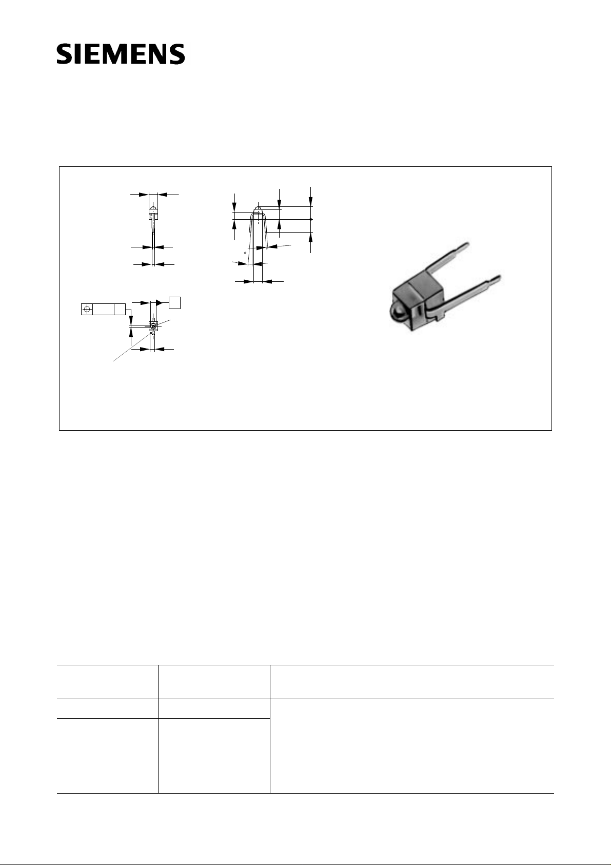
Collector (BPX 81)
Cathode (LD 261)
Detaching area for tools, flash not true to size.1)
Approx. weight 0.03 g
Maße in mm, wenn nicht anders angegeben/Dimensions in mm, unless otherwise specified.
0.7
0.6
A
Radiant sensitive area
(0.4 x 0.4)
1.4
1.0
position
1.9
1.7
5...0
2.54 mm spacing
2.7
0.25
0.15
2.1
1.5
2.5
GEO06021
3.6
3.5
3.2
3.0
LD 261
feo06021
Wesentliche Merkmale
● GaAs-IR-Lumineszenzdiode, hergestellt im
Schmelzepitaxieverfahren
● Hohe Zuverlässigkeit
● Gruppiert lieferbar
● Gehäusegleich mit BPX 81
Anwendungen
● Miniaturlichtschranken für Gleich- und
Wechsellichtbetrieb
● Lochstreifenleser
● Industrieelektronik
● “Messen/Steuern/Regeln”
Typ
Type
Bestellnummer
Ordering Code
Gehäuse
Package
Features
● GaAs infrared emitting diode, fabricated in a
liquid phase epitaxy process
● High reliability
● Available in bins
● Same package as BPX 81
Applications
● Miniature photointerrupters
● Punched tape readers
● Industrial electronics
● For control and drive circuits
LD 261 Q62703-Q395 Leiterbandgehäuse, klares Epoxy-Gießharz, linsenförLD 261-5 Q62703-Q67
mig im 2.54-mm-Raster (
1
/10’’), Kathodenkennzeich-
nung: Nase am Lötspieß
Lead frame, transparent epoxy resin lens, solder tabs
lead spacing 2.54 mm (1/10’’), cathode marking: projection at solder lead
Semiconductor Group 1 1997-11-01
Grenzwerte (TA = 25 °C)
Maximum Ratings
LD 261
Bezeichnung
Description
Betriebs- und Lagertemperatur
Operating and storage temperature range
Sperrschichttemperatur
Junction temperature
Sperrspannung
Reverse voltage
Durchlaßstrom
Forward current
Stoßstrom, τ≤10 µs,
D = 0
Surge current
Verlustleistung
Power dissipation
Wärmewiderstand
Thermal resistance
Symbol
Symbol
T
; T
op
stg
T
j
V
R
I
F
I
FSM
P
tot
R
thJA
R
thJL
Wert
Value
Einheit
Unit
– 40 ... + 80 °C
80 °C
5V
50 mA
1.6 A
70 mW
750
650
K/W
K/W
Kennwerte (
T
= 25 °C)
A
Characteristics
Bezeichnung
Description
Wellenlänge der Strahlung
Wavelength at peak emission
I
= 50 mA, tp = 20 ms
F
Spektrale Bandbreite bei 50 % von
Spectral bandwidth at 50 % of I
I
= 50 m A, tp = 20 ms
F
max
I
max
Abstrahlwinkel
Half angle
Aktive Chipfläche
Active chip area
Abmessungen der aktiven Chipfläche
Dimension of the active chip area
Abstand Chipoberfläche bis Linsenscheitel
Distance chip surface to lens top
Symbol
Symbol
λ
peak
Wert
Value
Einheit
Unit
950 nm
∆λ 55 nm
ϕ±15 Grad
deg.
A
L × B
L
× W
H
0.25 mm
0.5 × 0.5 mm
1.3 ... 1.9 mm
2
Semiconductor Group 2 1997-11-01
 Loading...