Siemens KSY46 Datasheet

Hall Sensor KSY 46
Preliminary Data
Features
• High sensitivity
• Small linearity error
• Low offset voltage
• Low TC of sensitivity
resistance
Typical Applications
• Current and power
measurement
• Magnetic field measurement
• Control of brushless DC
motors
• Rotation and position sensing
• Measurement of diaphragm
2.9
B
A
0.3
Reflow soldering
0.3
±0.1
1.9
+0.1
0.6
-0.05
64
5
1
23
+0.1
-0.05
0.8
±0.3
0.1
0.2
0.25MB
3
1.2
2˚ ... 30˚
1.1 max
0.08 ... 0.15
±0.1
10˚ max
2.6 max
10˚ max
0.35
0.1 max
M
0.20
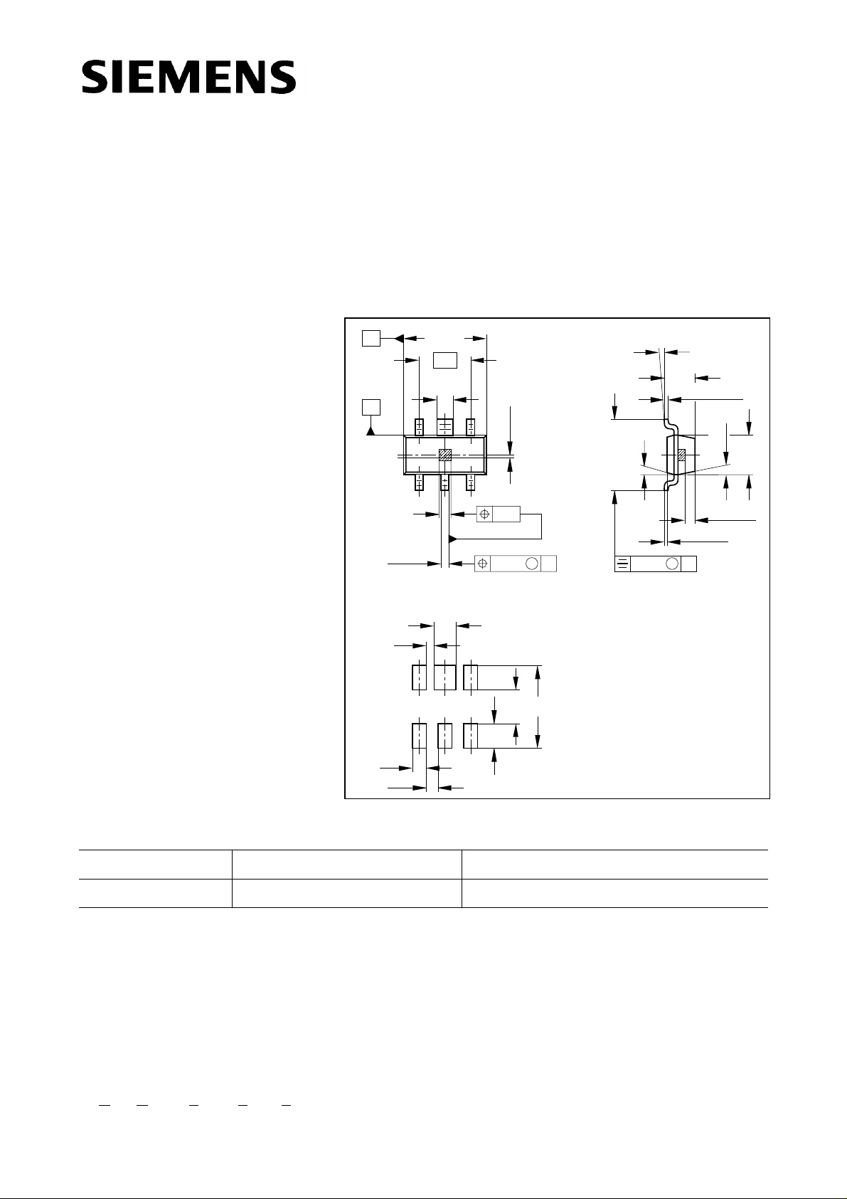
Approx. weight 0.02 g
Pin Configuration
1, 4 Hall voltage terminals
3+, 2/5- Supply current terminals
A
1.3
±0.15
0.9
0.5
0.45
Dimensions in mm
GPW06957
Type Marking Ordering Code
KSY 46 s46 on request
Packing: Taped on 18 cm reel, 3K parts per reel, date code on the label.
The KSY 46 is a MOVPE
1)
Hall sensor made of monocrystalline GaAs-material, built into
a SMT package (MW-6). The sensor is outstanding for its high magnetic field sensitivity
and its very low temperature coefficients. While the sensor is operated with constant
current, the output Hall Voltage is directly proportional to a magnetic field acting
prependicular to the surface of the sensor. The 0.35 × 0.35 mm
2
chip is mounted onto a
non-magnetic leadframe.
1) Metal Organic Vapour Phase Epitaxy
Semiconductor Group 1 1998-11-13

KSY 46
Maximum Ratings
Parameter Symbol Value Unit
Operating temperature
Storage temperature
Supply current
Thermal conductivity, soldered
in air
Characteristics (TA = 25 °C)
Nominal supply current
Open-circuit sensitivity
Open-circuit Hall voltage
I
= I1N, B = 0.1 T
1
Ohmic offset voltage
I
= I1N, B = 0 T
1
Linearity of Hall voltage
B = 0…0.5 T
B = 0…1.0 T
T
T
I
G
G
I
K
V
V
F
F
1
1N
A
stg
thC
thA
B0
20
R0
L
L
– 40 … + 150 °C
– 50 … + 160 °C
10 mA
≥ 2.2
≥ 1.5
mW/K
mW/K
7mA
150 … 265 V/AT
105 … 185 mV
≤ ± 15 mV
≤ ± 0.2
≤ ± 0.7
%
%
Input resistance
Output resistance
B = 0 T R
B = 0 T R
Temperature coefficient of the
open-circuit Hall-voltage
I
= I1N, B = 0.1 T
1
Temperature coefficient of the internal
resistance
B = 0 T
Temperature coefficient of ohmic offset
voltage
I
= I1N, B = 0 T
1
Switch on-drift of the ohmic offset
voltage
I
= I1N, B = 0 T
1
Noise Figure
1) dV0 = | V0 (t = 1 s) - V0(t = 0.1 s) |
∆V
2)
= | V0 (t = 3 m) - V0(t = 1 s) |
0
10
20
TC
TC
TC
dV
∆V
F
V20
R10, R20
VR 0
1)
0
2)
0
600 … 900 Ω
1000 … 1500 Ω
∼ – 0.03 %/K
∼ 0.3 %/K
∼ 0.3 %/K
≤ 0.3
≤ 0.1
mV
mV
∼ 10 dB
Semiconductor Group 2 1998-11-13
 Loading...